

Page 1

AN2472
Application note
STMAV340 analog video switch
Introduction
STMAV340 is a 4-channel SPDT high bandwidth, low Ron switch which provides a simple,
inexpensive means to switch high quality video signals without corrupting them. It is a
versatile video switch which can be used in multiple applications such as televisions,
notebooks, graphic cards and DVD players.
March 2007 Rev1 1/11
www.st.com
Page 2

Contents AN2472
Contents
1 Video switch parameters . . . . . . . . . . . . . . . . . . . . . . . . . . . . . . . . . . . . . 3
1.1 On-resistance (Ron) . . . . . . . . . . . . . . . . . . . . . . . . . . . . . . . . . . . . . . . . . . 3
1.2 Bandwidth . . . . . . . . . . . . . . . . . . . . . . . . . . . . . . . . . . . . . . . . . . . . . . . . . 3
1.3 Cross-talk and off-isolation . . . . . . . . . . . . . . . . . . . . . . . . . . . . . . . . . . . . . 3
1.4 Differential gain and phase . . . . . . . . . . . . . . . . . . . . . . . . . . . . . . . . . . . . . 4
1.5 Current consumption . . . . . . . . . . . . . . . . . . . . . . . . . . . . . . . . . . . . . . . . . 4
1.6 Delay measurements . . . . . . . . . . . . . . . . . . . . . . . . . . . . . . . . . . . . . . . . . 4
2 STMAV340 measurement set up . . . . . . . . . . . . . . . . . . . . . . . . . . . . . . . 5
2.1 Calibration . . . . . . . . . . . . . . . . . . . . . . . . . . . . . . . . . . . . . . . . . . . . . . . . . 5
2.2 Termination for bias . . . . . . . . . . . . . . . . . . . . . . . . . . . . . . . . . . . . . . . . . . 5
2.3 Measurement techniques . . . . . . . . . . . . . . . . . . . . . . . . . . . . . . . . . . . . . . 5
3 Advantages . . . . . . . . . . . . . . . . . . . . . . . . . . . . . . . . . . . . . . . . . . . . . . . . 6
4 Application information . . . . . . . . . . . . . . . . . . . . . . . . . . . . . . . . . . . . . . 7
4.1 Video display (TV) . . . . . . . . . . . . . . . . . . . . . . . . . . . . . . . . . . . . . . . . . . . 7
4.2 Notebook . . . . . . . . . . . . . . . . . . . . . . . . . . . . . . . . . . . . . . . . . . . . . . . . . . 7
4.3 Graphic cards . . . . . . . . . . . . . . . . . . . . . . . . . . . . . . . . . . . . . . . . . . . . . . . 8
4.4 DVD R/W . . . . . . . . . . . . . . . . . . . . . . . . . . . . . . . . . . . . . . . . . . . . . . . . . . 8
5 PCB layout considerations . . . . . . . . . . . . . . . . . . . . . . . . . . . . . . . . . . . . 9
5.1 Supply and ground effects . . . . . . . . . . . . . . . . . . . . . . . . . . . . . . . . . . . . . 9
5.2 PCB demo board . . . . . . . . . . . . . . . . . . . . . . . . . . . . . . . . . . . . . . . . . . . . 9
6 Conclusion . . . . . . . . . . . . . . . . . . . . . . . . . . . . . . . . . . . . . . . . . . . . . . . . . 9
7 Revision history . . . . . . . . . . . . . . . . . . . . . . . . . . . . . . . . . . . . . . . . . . . 10
2/11
Page 3

AN2472 Video switch parameters
1 Video switch parameters
1.1 On-resistance (Ron)
The on-resistance of the switch determines the propagation delay as well as the losses
suffered by the incoming signal. The higher on-resistance of the switch increases the
insertion loss making the use of a buffer/gain-stage inevitable. Since the analog voltage
level for most video signals lies between 0 V and 1 V, the s witch must provide a minimum
R
within this range. The higher value of the resistance will reduce the gain, add noise and
on
increase the propagation delay. Thus it is desirable to have the on-resistance of the video
switch only in the range of a few ohms. It is worth mentioning here that to achieve a lower
R
, the pass transistor has to be large which gives a higher capacitance, thus limiting the
on
bandwidth of the de vice . Thus a good tr ade-o ff bet ween the R
an important consideration in the design of an analog video switch.
If the on-resistance of the s witch is higher, the need to use an amplifier is larger as there is a
higher voltage drop across the switch.
1.2 Bandwidth
and channel capacitance is
on
The bandwidth of the video switch is an important parameter as it determines the signal
quality at the output. The higher bandwidt h of t he switch allows the signal at the input of the
switch to be reproduced at its outpu t with minimum distortion on the edges and the
amplitude. The amplitude distortion is due to the losses through the switch, parasitic
resistances, and capacitances while the edge dist ortion comes mainly from the capacitance.
The high bandwidth of the switch maintains the high fidelity of the analog video signal.
The higher the bandwidth in the system, the higher is the detail in the video signal. The
highest frequency of the video signal depends on the rise/fall time of the signal. The
bandwidth of a video signal is a complex fu nction depending on several factors like the
aspect ratio, number of vertical scan lines, frame rate or refresh rate and the ratio of total
horizontal/vertical pixels t o act ive ones. The circuit that processes the video si gna l n eed s t o
have more bandwidth t han the actual bandwidth of the processed signal to minimize the
degradation of the signal and the resulting loss in picture quality. The amount of circuit
bandwidth needs to exceed the highest frequency in the signal to reproduce a high-quality
signal. Depending upon the attenu ation of t he signal at t he output , the cir cuit band width has
to be 3-6 times higher than the maximum fre quency in the video signal. In addition to the
bandwidth, the circuit must slew fast enough to faithfully reproduce the video signal.
1.3 Cross-talk and off-isolation
It is seen during the crosstalk measurement that the termination on other ports can
significantly affect the crosstalk measured value on a port. When the unused ports are unterminated (left open) the value of the crosstalk measure d is worse than when the unused
ports are terminated with proper 75 Ohm loads. Thus it is necessary to terminate the
unused ports with proper loads for an accurate cr osstalk measurement (similar to a real
application environment). Th is also ap plies to t he o ff- iso lat ion parameter. The higher the o ffisolation value, the better the switch separates the active data from the non-active display
terminals.
3/11
Page 4

Video switch parameters AN2472
1.4 Differential gain and phase
Differential gain and differential phase refer to how the video switch attenuates the signal
differently for inputs biased at various DC levels.
This specification is associated with R
occurring with a smaller differential gain. A lesser variation of on capacitance of a video
switch over various DC biases results in a lower different ial phase.
The differential gain and phase are further defined as below:
Differential gain is the perce ntage error in the magnitude/amplitude change in the analog
output voltage from t he analog input v oltage when the input is betw een 0 V and 0.714 V and
the switch is enabled. Load at the output is 150 Ohm. 0 V and 0.714 V represents the DC
offset.
Differential gain is expressed in % error and is calculated as follows:
● Reference gain (when input bias is 0 V, f=3.58 MHz) = V
dB = G1 (say)
● New gain (when input bias is 0.714V, f=3.58MHz) = V
dB = G2 (say)
● Then Error = E = G2 - G1 (dB)
● % Error in Gain = Differential Gain = 100 * Antilog (E/20)
The differential phase is measured in a sim ilar way from the AC/transient simulation plot.
1.5 Current consumption
There are two parts to the current, one comes from the current consumed by the logic
control circuit and the other is b y the s witch itself . Th e supply of the de vice is only conn ected
to the logic control part (switch enab le an d selecti on) . The analo g p ulsing inp ut vide o sig nal
is the other source of voltage to the video switch.
flatness over the 1.0V range, with more flatness
on
= 20 log (V
out/Vin
//Vin = 20 log (V
out
out/Vin
//Vin)
out
)
The current consumption of the s witch wh en it is act ive but not switching is only dete rmined
by the static current through the logic part of the device. When it is switching, the current is
determined by the logic control elements of the switch.
The input voltage source to the switches' drain/source and the load attached at the switch
output determine the current through the switch itself.
During the standby state, the current consumption of the switch drops to very low and is
practically negligible.
1.6 Delay measurements
The magnitude of the R
The delay measurements include the switch turn-on / turn-off times and the propagation
delays. The measurement is done using the load circuit as shown in the datasheet. For the
waveforms and the timing specifications, refer to the STMAV340 datasheet.
4/11
on
and C
determine the propagation delay of the switch.
on
Page 5

AN2472 STMAV340 measurement set up
2 STMAV340 measurement set up
2.1 Calibration
This is one of the most critical parts to good measurement. The AC parame ters of the s witch
are measured using a network analyzer which must be properly calibrated before use. The
calibration is done on the equipment i tself and then with th e board. Through , open and short
calibration are performed without the DUT placed on the board or with DUT enabled on the
board and with both the input and output ports of the network analyzer connected to the
switch connectors on the board. After the calibration is done, the channel output on the
analyzer is stable and is not affected by any movements of the cables or the board. This
also helps to ensure that the calibration is performed by taking the DUT and board into
account. Initially if desired the calibration can be run by conne ct ing the two ports together.
2.2 Termination for bias
In a typical video application the bias is needed to provide the DC offset required for the
video signal. The decoupling capacitor filters the negative part of the video signal before it
reaches the switch. The input s and outputs of th e s witch ha v e to be terminated with 75 Ohm
resistors to eliminate any reflections due to impedance mismatches betwe en the source and
the sink.
The parameters are measured with 150 Ohm load as the series resistor of 75 Ohm of the
cable is in series with the far-end termination resistor of 75 Ohm, adding them up to
150 Ohm.
2.3 Measurement techniques
Proper measurement methods and stab le test set-up ensure th at the real de vice parameters
are measured during the characterization of the device. Good contacts of the cable
assemblies to the SMA connectors on the board must be present. Care is taken to ensure
that the probes of the equipment a re ti ghtly screwed to the equipment and the device under
test (D.U.T.). Soldering with a good shining solder dot without any dry solder gives a robust
low resistance contact for the signals on the board.
5/11
Page 6
Advantages AN2472
3 Advantages
The low on-resistance and capacitance of the switch make it very suitable for highbandwidth signal switchin g like video signals.
The high off-isolation provides e xce llent isola tio n at high fr equen cie s when t he video switch
is open.
The low crosstalk gives excellent isolation between channels to prevent unwanted
interference.
The low differential gain/phase of the switch means very low signal distortion and excellent
R
matching.
on
The TSSOP16 package with a pitch of 0.65mm allows easy mounting and assembly on the
PCB board.
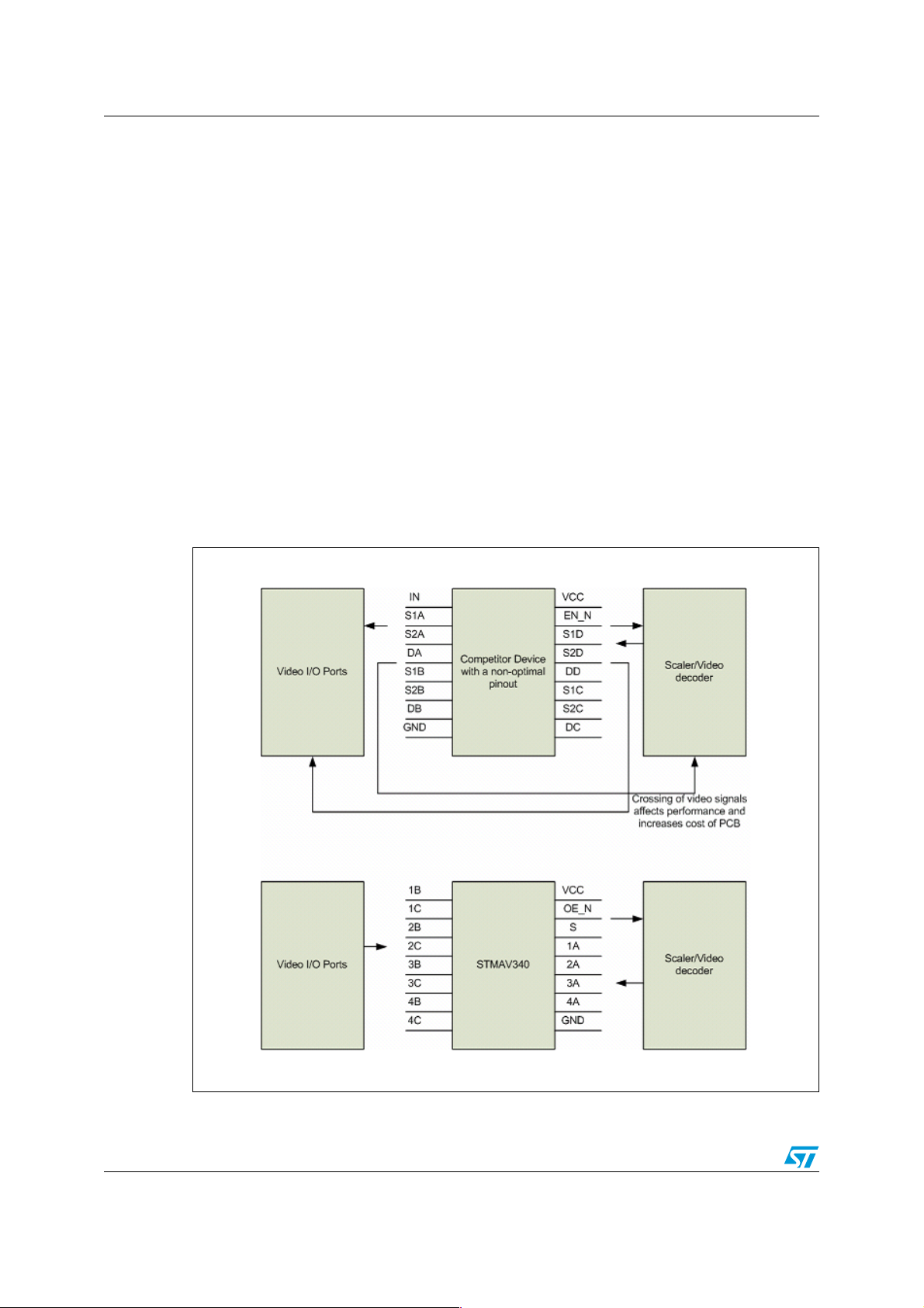
A major advantage of this product over the competitors' product is that the inputs and
outputs of the switch are on either sides which allow easy PCB routing that leads to saving a
layer on PCB, thus reducing cost and improving performance at the same time. This is
highlighted in the Figure 1.
Figure 1. Simple PCB design using STMAV340
6/11
Page 7

AN2472 Application information
4 Application information
The switch can be used in a wide array of applications as shown in the below section. The
only difference is the way the switching is accomplished (mux or de-mux) and the type of
signals which are needed by different applications.
4.1 Video display (TV)
The main application of the switch is in the displays like the CRT TV, LCD TV and Mon itor.
Figure 2. Application of STMAV340 in a video display
4.2 Notebook
In a PC application, the video switch can be used to multiplex RGB signals between a
notebook and its docking station. Use of a 3-bit/3-channel SPDT analog video switch in this
application eliminates a redundant graphics chip in the docking station, thus reducing cost,
component count and complexity.
Figure 3. Application of STMAV340 in a notebook
7/11
Page 8

Application information AN2472
4.3 Graphic cards
Sometimes graphic cards in PCs can be used to drive multiple displays. In such cases, the
display loading of the RAMDAC output is increased. This increased load will not only
degrade the signal quality as voltage levels will be reduced, but also may require
buffer/a mplifier which increases the cost and comple xity. One wa y to accommod ate multiple,
simultaneously connected displays to a single graphics chip is through the use of
STMAV340 as depicted in Figure 4.
Figure 4. Application of STMAV340 in graphic cards
4.4 DVD R/W
The STMAV340 can also be used in DVD R/W applications to multiplex the DVD R/W
signals and the CD signals between the Optical pick up unit and the main controller.
Figure 5. Application of STMAV340 in multiplexing DVD R/W and CD signals
8/11
Page 9

AN2472 PCB layout considerations
5 PCB layout considerations
The decoupling capacitors should be placed as close as possible to the supply pins of the
device as it helps to minimiz e the noise due to s witching and other sources. It is important to
ensure that the PCB tracks have resistances of 75 Ohm and are well matched fo r all the
inputs and outputs. This minimizes the impedance discontinuities between the analyzer
probes and measurement points on the board and thus reduces the reflections. From an
application perspective , image ghosting may occur if there is an impedance mismatch. The
75 Ohm termination on both the sides of the switch is provided by the network analyzer
itself. Load capacitance is placed close to the output pins of the device when required for
respective measurements.
5.1 Supply and ground effects
Placing decoupling capacitors close to the VDD and GND pins of the device help in good
noise isolation and decoupling. For both high and low frequency noise filtering, a 10 µF
electrolytic capacitor is placed in parallel with a 100 nF ceramic capacito r . The g round plane
and good solid connections to it significantly improve the performance of the device. It is a
good practice to place as many vias from the top layer to the ground plane as possible to
lower the resistance betw een the contact and the ground plane, thereby reducing noise.
5.2 PCB demo board
This board is manufactured to do real video signal application level tests. A typical
configuration of the switch is shown below (to be added) for the tests. The BOM and the
board schematics + layout files (Gerber files) are available upon request and will be placed
in the Appendix section of the application note. The PCB demo board allows switching
between RGB, YPbPr inputs and also two composite (CVBS) inputs. The inputs come from
the video sources and the output of the s witch is connected to the displa y de vice like a TV or
PC monitor.
6 Conclusion
In this way a single product finds use in a wide r ange of applications t o serve va rious needs.
ST's STMAV340 is a perfect low-cost, high-performance solution which provides system
developer s with simple and eff ectiv e wa ys to do video signal s witching without impact ing the
quality of the image.
9/11
Page 10

Revision history AN2472
7 Revision history
Table 1. Revision history
Date Revision
14-Mar-2007
Changes
1
First issue
10/11
Page 11

AN2472
Please Read Carefully:
Information in this document is provided solely in connection with ST products. STMicroelectronics NV and its subsidiaries (“ST”) reserve the
right to make changes, corrections, modifications or improvements, to this document, and the products and services described herein at any
time, without notice.
All ST products are sold pursuant to ST’s terms and conditions of sale.
Purchasers are solely res ponsibl e fo r the c hoic e, se lecti on an d use o f the S T prod ucts and s ervi ces d escr ibed he rein , and ST as sumes no
liability whatsoever relati ng to the choice, selection or use of the ST products and services described herein.
No license, express or implied, by estoppel or otherwise, to any intellectual property rights is granted under this document. If any part of this
document refers to any third pa rty p ro duc ts or se rv ices it sh all n ot be deem ed a lice ns e gr ant by ST fo r t he use of su ch thi r d party products
or services, or any intellectua l property c ontained the rein or consi dered as a warr anty coverin g the use in any manner whats oever of suc h
third party products or servi ces or any intellectual property contained therein.
UNLESS OTHERWISE SET FORTH IN ST’S TERMS AND CONDITIONS OF SALE ST DISCLAIMS ANY EXPRESS OR IMPLIED
WARRANTY WITH RESPECT TO THE USE AND/OR SALE OF ST PRODUCTS INCLUDING WITHOUT LIMITATION IMPLIED
WARRANTIES OF MERCHANTABILITY, FITNESS FOR A PARTICUL AR PURPOS E (AND THEIR EQUIVALE NTS UNDER THE LAWS
OF ANY JURISDICTION), OR INFRINGEMENT OF ANY PATENT, COPYRIGHT OR OTHER INTELLECTUAL PROPERTY RIGHT.
UNLESS EXPRESSLY APPROVED IN WRITING BY AN AUTHORIZED ST REPRESENTATIVE, ST PRODUCTS ARE NOT
RECOMMENDED, AUTHORIZED OR WARRANTED FOR USE IN MILITARY, AIR CRAFT, SPACE, LIFE SAVING, OR LIFE SUSTAINING
APPLICATIONS, NOR IN PRODUCTS OR SYSTEMS WHERE FAILURE OR MALFUNCTION MAY RESULT IN PERSONAL INJ URY,
DEATH, OR SEVERE PROPERTY OR ENVIRONMENTAL DAMAGE. ST PRODUCTS WHICH ARE NOT SPECIFIED AS "AUTOMOTIVE
GRADE" MAY ONLY BE USED IN AUTOMOTIVE APPLICATIONS AT USER’S OWN RISK.
Resale of ST products with provisions different from the statements and/or technical features set forth in this document shall immediately void
any warranty granted by ST fo r the ST pro duct or serv ice describe d herein and shall not cr eate or exten d in any manne r whatsoever , any
liability of ST.
ST and the ST logo are trademarks or registered trademarks of ST in various countries.
Information in this document su persedes and replaces all informati on previously supplied.
The ST logo is a registered trademark of STMicroelectronics. All other names are the property of their respective owners.
© 2007 STMicroelectronics - All rights reserved
STMicroelectronics group of compan ie s
Australia - Belgium - Brazil - Canada - China - Czech Republic - Finland - France - Germany - Hong Kong - India - Israel - Italy - Japan -
Malaysia - Malta - Morocco - Singapore - Spain - Sweden - Switzerland - United Kingdom - United States of America
www.st.com
11/11
 Loading...