

Page 1
AN2459
Applica t ion note
Digital Power Factor Correction for Tube Lamp Ballasts and
other digital power supplies controlled by an 8-bit microcontroller
1 Introduction
The electronic ballast market has undergone dramatic changes over the last few years. It
has moved from full analog, very differentiated applications made by a collection of drivers
and controllers, where use of custom ASICs was widespread, to a couple of standard
platforms.
The basic building bloc ks are st i ll the same. They include a power factor corrector s tage and
an inverting high voltage stage (Figure 1). On the one hand, analog platforms are targeting
the low cost/basic performance applications. Their main drivers and controllers are widely
used and well known ICs such as Power Factor Correctors (L6561/2/3) and High Voltage
Ballast Controllers (L6569x/ L6571x/ L6574). On the other hand, a new digital platform
concept has gained more interest and acceptance. A microcontroller with a simple Half
Bridge Driver (L638x) has replaced the ballast controller. The Half Bridge Driver is used
mainly for high-end applications, especially where the microcontroller has to deal with
communication tasks (e.g. using the Dali protocol).
STMicroelectronics' digital ballast reference design STEVAL-ILB002V1 introduces a safe
operating Power Factor Controller (PFC) and Ballast Controller. Even with relatively simple
microcontroller firmware routines, the results for power control and ballast protection are in
line with advanced analog controlled ballasts, while adding flexibility, for example, the
possibility to drive a wide variety of lamps, or to easily introduce different protection
schemes.
This application note deals in detail with the first block of the digital ballast, which provides
stable DC bus voltage for the halfbridge in all load conditions, as well as controlling the input
current shape which fulfills IEC standards (6.: IEC 61000-3-2 "Electromagnetic
compatibility".).
The final description of the digital ballast - the lamp control block - will be described in detail
in a separate application note.
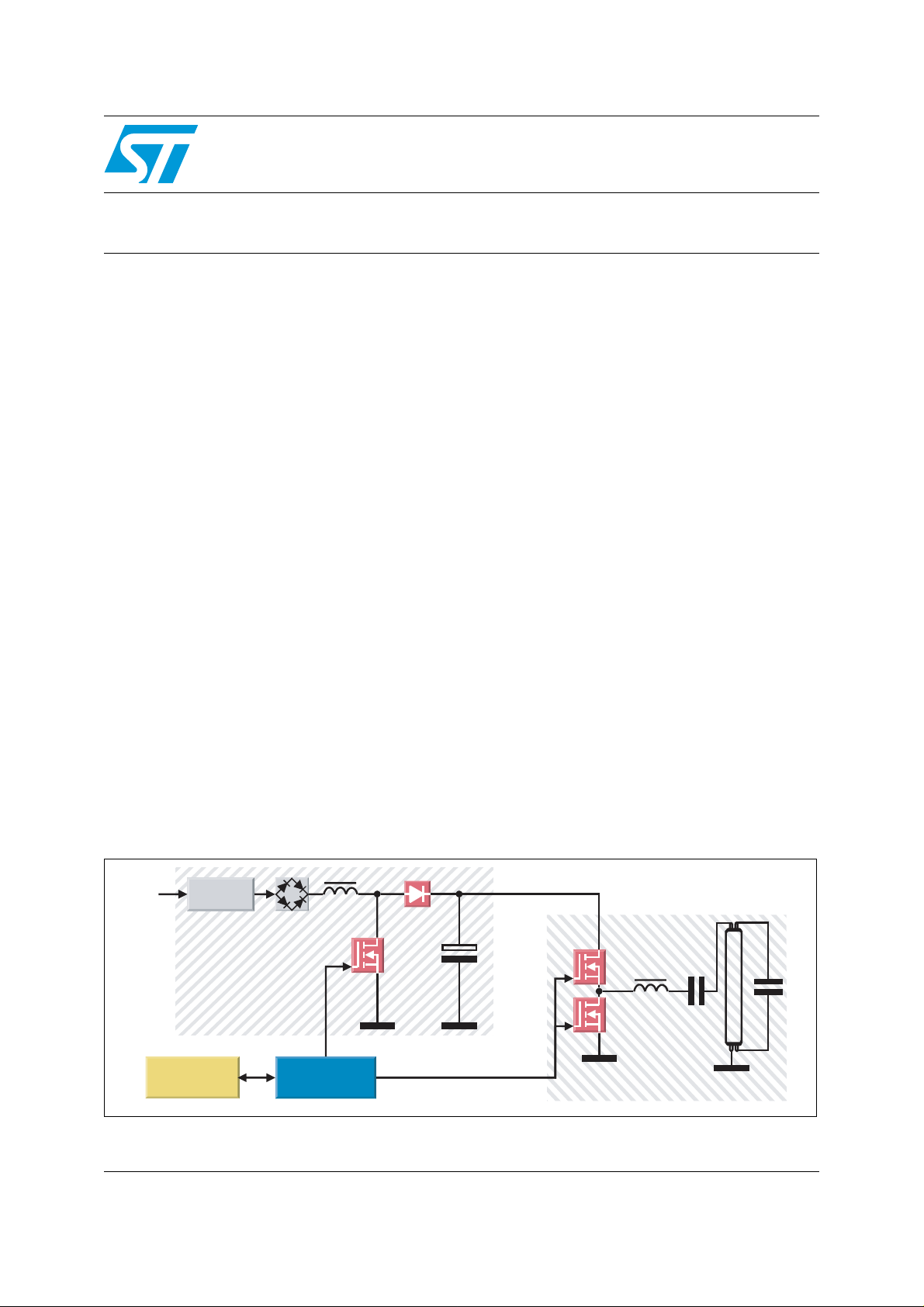
Figure 1. Digital ba llast scheme
Input Filter
8-Bit
Microcontroller
ST7FLITE19B
January 2007 Rev 1 1/35
Power
Management
L6382D5
Unit
www.st.com
Page 2

Contents AN2459 - Application note
Contents
1 Introduction . . . . . . . . . . . . . . . . . . . . . . . . . . . . . . . . . . . . . . . . . . . . . . . . 1
2 Power Factor Correction (PFC) . . . . . . . . . . . . . . . . . . . . . . . . . . . . . . . . 5
2.1 Transition Mode operation . . . . . . . . . . . . . . . . . . . . . . . . . . . . . . . . . . . . . 5
2.2 Digital implementation - Enhanced One Pulse Mode . . . . . . . . . . . . . . . . . 6
3 Power circuits design . . . . . . . . . . . . . . . . . . . . . . . . . . . . . . . . . . . . . . . . 8
3.1 Power components . . . . . . . . . . . . . . . . . . . . . . . . . . . . . . . . . . . . . . . . . . . 8
3.2 Schematics . . . . . . . . . . . . . . . . . . . . . . . . . . . . . . . . . . . . . . . . . . . . . . . . 10
3.3 Bill of material (STEVAL-ILB002V1) . . . . . . . . . . . . . . . . . . . . . . . . . . . . . 12
4 Signals measurement, processing & control . . . . . . . . . . . . . . . . . . . . 15
4.1 Input vo ltage . . . . . . . . . . . . . . . . . . . . . . . . . . . . . . . . . . . . . . . . . . . . . . . 16
4.2 Output voltage . . . . . . . . . . . . . . . . . . . . . . . . . . . . . . . . . . . . . . . . . . . . . 18
4.3 Zero Current Detection . . . . . . . . . . . . . . . . . . . . . . . . . . . . . . . . . . . . . . . 21
4.4 MOSFET current measurement . . . . . . . . . . . . . . . . . . . . . . . . . . . . . . . . 23
5 Conclusion and outlook . . . . . . . . . . . . . . . . . . . . . . . . . . . . . . . . . . . . . 26
6 References and related materials . . . . . . . . . . . . . . . . . . . . . . . . . . . . . 27
Appendix A Components calculation. . . . . . . . . . . . . . . . . . . . . . . . . . . . . . . . . . 28
A.1 Input capacitor. . . . . . . . . . . . . . . . . . . . . . . . . . . . . . . . . . . . . . . . . . . . . . 28
A.2 Output capacitor . . . . . . . . . . . . . . . . . . . . . . . . . . . . . . . . . . . . . . . . . . . . 28
A.3 Boost inductor. . . . . . . . . . . . . . . . . . . . . . . . . . . . . . . . . . . . . . . . . . . . . . 29
A.4 Power MOSFET . . . . . . . . . . . . . . . . . . . . . . . . . . . . . . . . . . . . . . . . . . . . 32
A.5 Boost Diode. . . . . . . . . . . . . . . . . . . . . . . . . . . . . . . . . . . . . . . . . . . . . . . . 33
7 Revision history . . . . . . . . . . . . . . . . . . . . . . . . . . . . . . . . . . . . . . . . . . . 34
2/35
Page 3

AN2459 - Application note List of tables
List of tables
Table 1. Bill of material - PFC. . . . . . . . . . . . . . . . . . . . . . . . . . . . . . . . . . . . . . . . . . . . . . . . . . . . . . 12
Table 2. Bill of material - Lamp Control . . . . . . . . . . . . . . . . . . . . . . . . . . . . . . . . . . . . . . . . . . . . . . 13
Table 3. Bill of material - general . . . . . . . . . . . . . . . . . . . . . . . . . . . . . . . . . . . . . . . . . . . . . . . . . . . 14
Table 4. Document revision history . . . . . . . . . . . . . . . . . . . . . . . . . . . . . . . . . . . . . . . . . . . . . . . . . 34
3/35
Page 4

List of figures AN2459 - Application note
List of figures
Figure 1. Digital ballast sch eme. . . . . . . . . . . . . . . . . . . . . . . . . . . . . . . . . . . . . . . . . . . . . . . . . . . . . . 1
Figure 2. PFC Transition Mode principle (frequency is not to scale) . . . . . . . . . . . . . . . . . . . . . . . . . . 6
Figure 3. Principle of the Enhanced One Pulse Mode, inside the ST7Lite1B . . . . . . . . . . . . . . . . . . . 7
Figure 4. Input voltage & current with modified EMI filter
(compared to STEVAL-ILB002V 1) PF = 0.994 THD = 10.3% . . . . . . . . . . . . . . . . . . . . . . . 8
Figure 5. Input voltage & current measured on STEVAL-ILB002V1 (old EMI filter)
PF = 0.991 THD = 10.4% . . . . . . . . . . . . . . . . . . . . . . . . . . . . . . . . . . . . . . . . . . . . . . . . . . 9
Figure 6. Schematics of STEVAL-ILB002V1 reference des i gn . . . . . . . . . . . . . . . . . . . . . . . . . . . . . 10
Figure 7. Modified EMI filter (not included in STEVAL-ILB002V1 reference design . . . . . . . . . . . . . 11
Figure 8. General flowchart of PFC software. . . . . . . . . . . . . . . . . . . . . . . . . . . . . . . . . . . . . . . . . . . 15
Figure 9. Input voltage sensing circuit . . . . . . . . . . . . . . . . . . . . . . . . . . . . . . . . . . . . . . . . . . . . . . . . 16
Figure 10. Inpu t voltage sensing circuit output . . . . . . . . . . . . . . . . . . . . . . . . . . . . . . . . . . . . . . . . . . 17
Figure 11. The mains turn-on . . . . . . . . . . . . . . . . . . . . . . . . . . . . . . . . . . . . . . . . . . . . . . . . . . . . . . . 18
Figure 12. Out put voltage sensing circuit. . . . . . . . . . . . . . . . . . . . . . . . . . . . . . . . . . . . . . . . . . . . . . . 19
Figure 13. Out put v oltage control loop flowchart . . . . . . . . . . . . . . . . . . . . . . . . . . . . . . . . . . . . . . . . . 19
Figure 14. Application start-up . . . . . . . . . . . . . . . . . . . . . . . . . . . . . . . . . . . . . . . . . . . . . . . . . . . . . . 20
Figu r e 1 5 . Lamp re s tart - behavi o r o f the con t r o l lo o p . . . . . . . . . . . . . . . . . . . . . . . . . . . . . . . . . . . . . 21
Figure 16. Zero current crossing dete ction . . . . . . . . . . . . . . . . . . . . . . . . . . . . . . . . . . . . . . . . . . . . . 22
Figure 17. PFC M OSFET overcurrent detection circuit and zero coil current detection circuit with
indicated testing connection and microcontroller inner structure . . . . . . . . . . . . . . . . . . . . 24
Figu r e 1 8 . Maxim u m MOSFET's TON p r o tection routine . . . . . . . . . . . . . . . . . . . . . . . . . . . . . . . . . . 24
Figure 19. Overcurrent reaction demonstration. . . . . . . . . . . . . . . . . . . . . . . . . . . . . . . . . . . . . . . . . . 25
4/35
Page 5

AN2459 - Application note Power Factor Correction (PFC)
2 Power Factor Correction (PFC)
Theoretically, any switching topology can be used to achieve a hi gh power factor but, in
practice, the boost topology has become the most popular because of the advantages it
offers. These include:
● Circuit requires the least external parts, thus it is the cheapest available.
● Boost inductor, located between the bridge and the switch, lowers the input di/dt, thus
minimizing noise generated at the input and consequently reducing the EMI filter input
requirements.
● Switch is source-grounded and therefore easy to drive.
Three methods of controlling the PFC preregulator are currently widely used. They are:
● T he Fixed Frequency Average Current Mode PWM.
● The Transition Mode (TM) PWM (fixed on-time, variable frequency).
● The peak current mode with fixed off-time.
Control of the first method is complicated and requires a sophisticated IC controller (e.g.
either ST's L4981A or ST’s L4981B which offers frequency modulation) and a considerable
component count.
Control of the second method is simpler (e.g. ST's L6561/2/3 family) and requires fewer
external parts. It is therefore much less expensive.
With the Fixed Fre quency Average Current Mode method, the boost inductor operates in
continuous conduction mode, while the TM method causes the inductor to work on the
boundary between continuous and discontinuous modes. Thus, for a given throughput
power, TM operation involves higher peak c urrents, suggesting it is more efficient at lower
power ranges (typically below 200W). In contrast, the Fixed Frequency Average Current
Mode is recommended for higher power levels.
A third method of control, that of applying constant. Toff control, results in continuous
conduction mode. The same simple TM-controllers may be used, as may a small RC
network to set the off-time. This method is described in AN1792 (7) It is optimal for an input
power of between 200 and 400W.
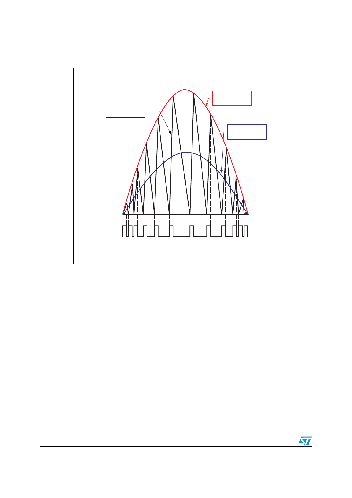
2.1 Transition Mode operation
As mentioned above, the typical PFC topology used in electronic ballasts is a step-up
(boost) regulator (Figure 1) working in transition conduction mode. Figure 2 outlines the
Transition Mode principles. When the MOSFET is turned on, the inductor is charged from
the input voltage source. When the MOSFET is turned off, the boost inductor discharges its
energy into the load until its current falls to zero. When the latter occurs, the boost inductor
has no energy and a zero current (ZCD) signal is detected, due to a demagnetization
change on the auxiliary winding. This drives the MOSFET on again, whereby another
conversion cycle starts. As the drain voltage drops before turn-on, the turn-on switching
losses are minimized. Figure 2 indicates the geometric relationship of average and peak
currents. Due to the triangular shape of the inductor current, the peak current is twice the
average current.
5/35
Page 6
Power Factor Correction (PFC) AN2459 - Application note
Figure 2. PFC Transition Mode principle (frequency is not to scale)
Peak current
enveloppe
Inductor current
Average current
On
MOSFET
On
2.2 Digital implementation - Enhanced One Pulse Mode
To provide good switch control, as described in Chapter 2.1 above, a simple 8-bit
microcontroller may be used and a special PWM timer mode has been introduced. The
timer mode, called "Enhanced One Pulse Mode" of the PWM generator (12-bit autoreload
timer) is found inside the ST7FLITE19B microcontroller. It is explained in Figure 3 and in
datasheet ST7Lite1xB (4). In principle, when a zero current e v ent occurs the microcontroller
will reset the timer and turn -on the PFC MOSFE T. If there is no signal from ZCD, the timer
will overflow and turn-on the MOSFET anyway (it means a minimum switching frequency is
secured). The on-time of the MOSFET is set by a software control routine and is constant
during the mains half-cycle (this is detailed below in Chapter 4). The control routine
executed by the MCU alters the on-time depending on the input voltage level and the load
current.
AI12647
6/35
Page 7

AN2459 - Application note Power Factor Correction (PFC)
Figure 3. Principle of the Enhanced One Pulse Mode, inside the ST7Lite1B
Compare event
Timer
Events ignored, because
MOSFET is turned-on
ZCD
On
MOSFET
Off
Timer reset caused by
ZCD
Event
Timer reset caused by
autoreload value match
Event
No event
occured
}
AI12651
7/35
Page 8
Power circuits design AN2459 - Application note
3 Po wer circuits design
3.1 Power components
All components have been calculated following application note AN966 (3). A full description
of the design and selection of each component, based on the analog TM PFC controller
L6561, is also given in Appendix A. At the moment, input voltage is limited for European
mains. Future Software updates will include wide range input capability.
Besides the passive and discrete components of the microcontroller, the most important
part is the power management unit, L6382D5, which helps control the power. It provides a
stable (±2%) 5V supply for the microcontroller during the whole operation. It also supplies a
high voltage start-up. In addition, one of the general purpose gate drivers integrated inside
L6382D5 is used to translate TTL PWM signals from the microcontroller to the boost
converter gate of the MOSFET.
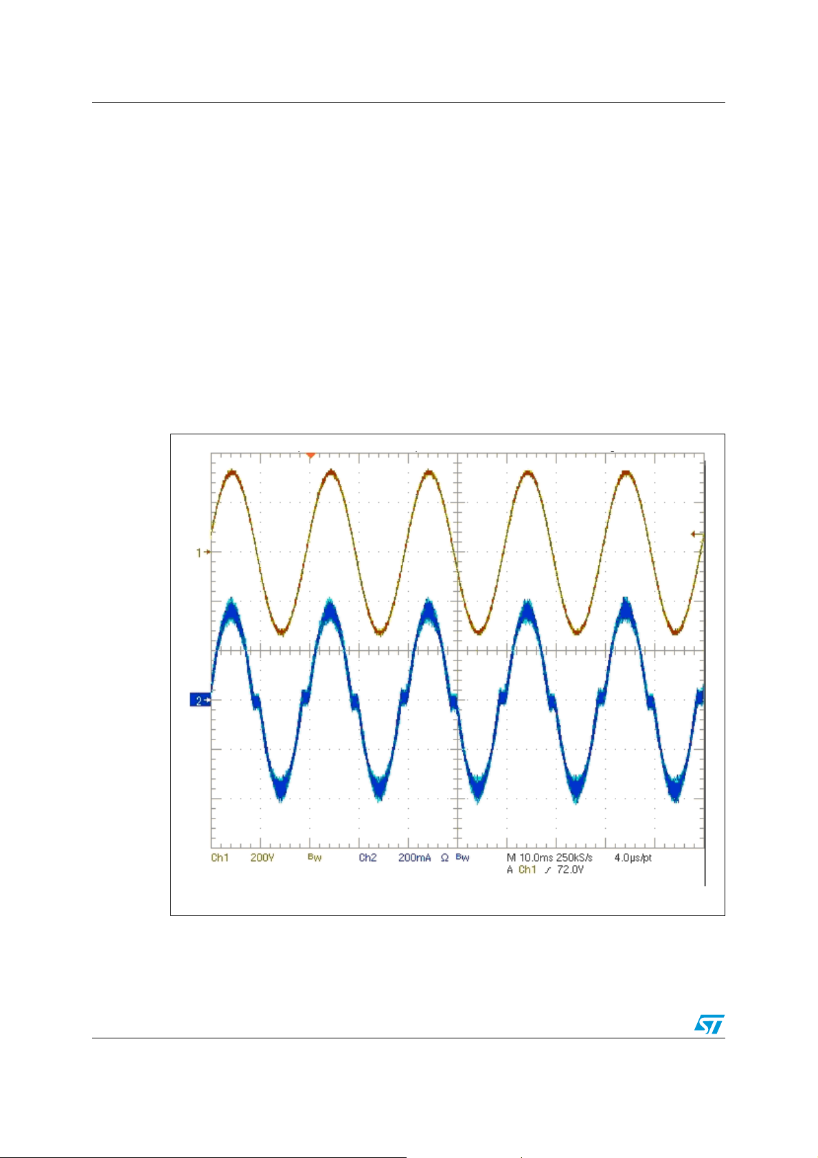
Figure 4. Input voltage & current with modified EMI filter
(compared to STEVAL-ILB002V1) PF = 0.994 THD = 10.3%
Note: Brown = Mains voltage, Blue = Input current.
8/35
Page 9
AN2459 - Application note Pow er cir cuits d esign
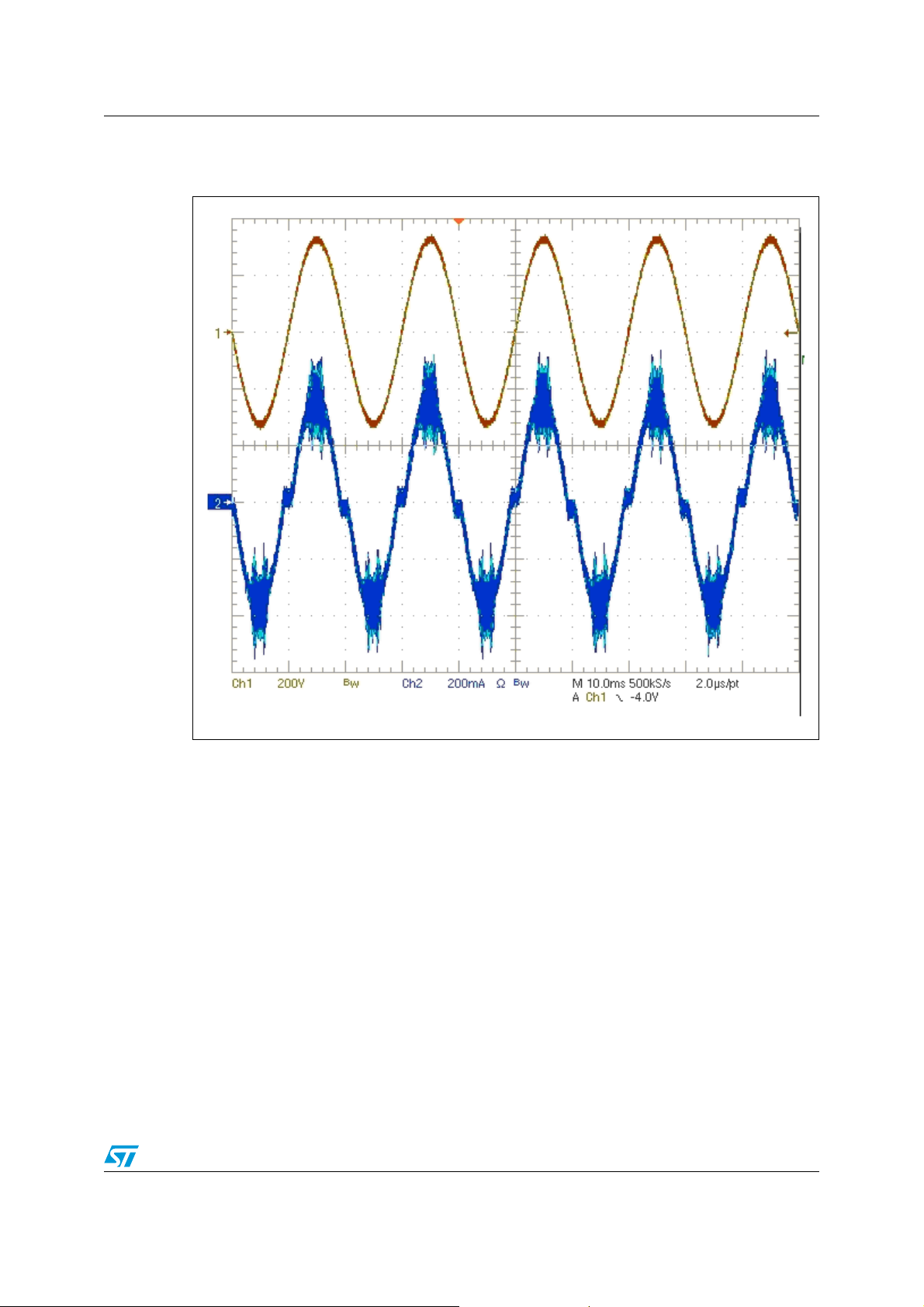
Figure 5. Input voltage & current measured on STEVAL-ILB002V1 (old EMI filter)
PF = 0.991 THD = 10.4%
Note: Brown = Mains voltage, Blue = Input current.
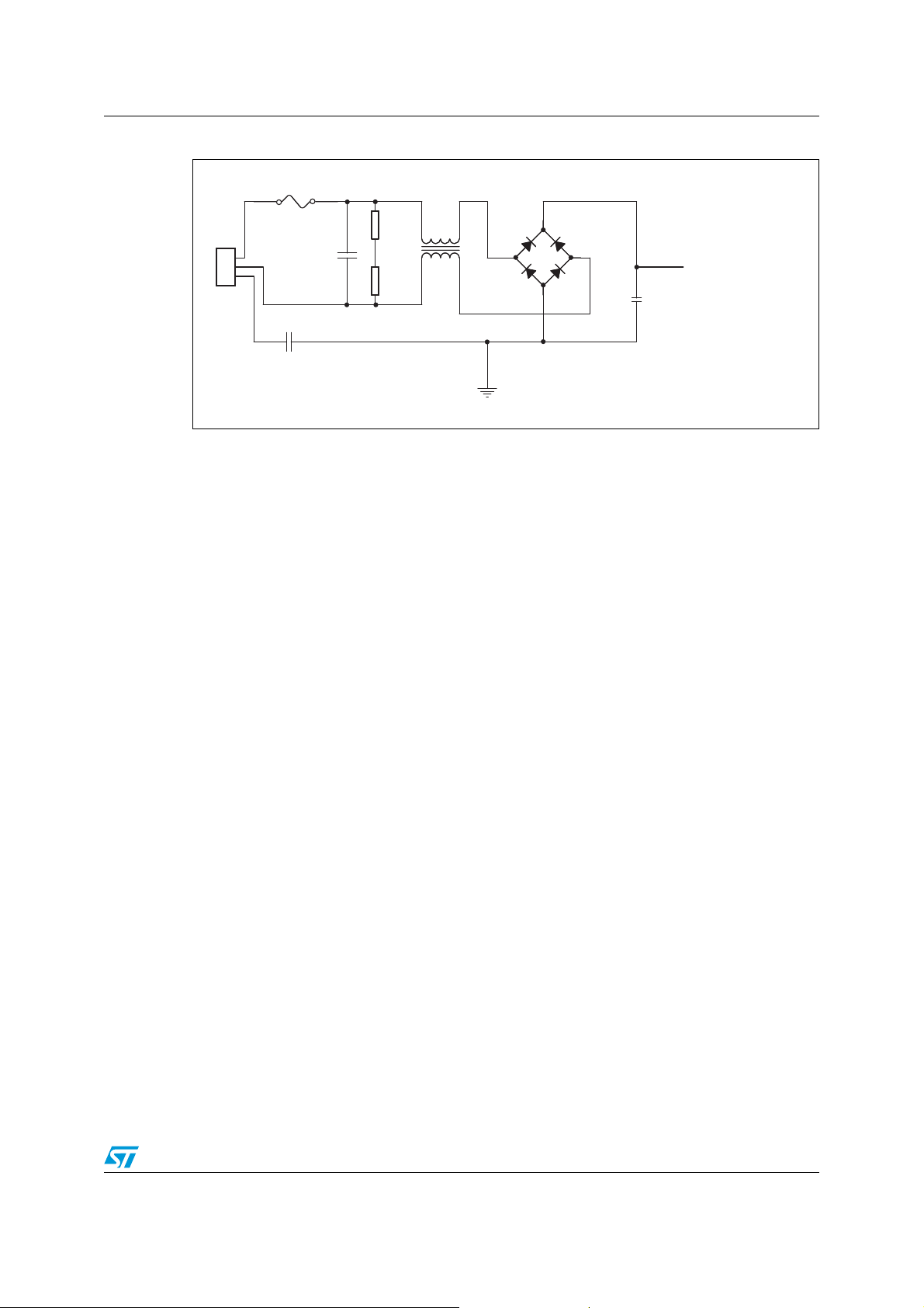
Reference board design measurements of STEVAL-ILB002V1(Figure 5) show a THD value
of 10.4% and a PF value of 0.991. Between the manufacturing of the STEVAL-ILB002V1
reference design and publication of this application note, design work has continued and
some improvements have been made. For example, EMI filter parameters have been
changed from C-L-C to C-L filters, which give better results for waveform, power factor, and
THD .This optimized version is given in Figure 7 and result in the measured waveforms
shown in Figure 4 with THD = 10.3% and PF = 0.994.
9/35
Page 10
Power circuits design AN2459 - Application note
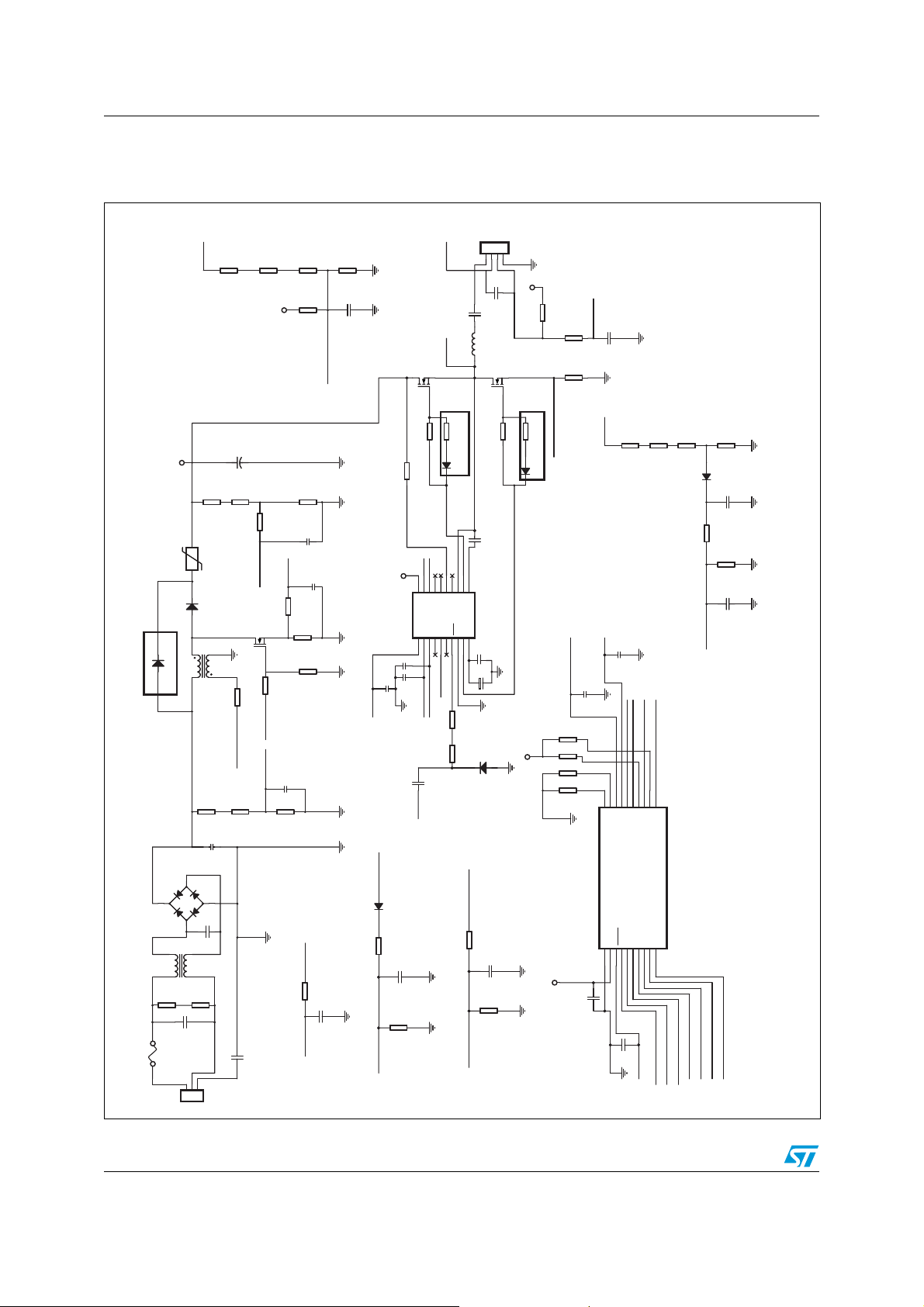
3.2 Schematics
Figure 6. Schematics of STEVAL-ILB002V1 reference design
CC
C11
J2
123
1.8mH
C13
L6382
C12
100nF
47µF
25V
+
+
D13
STTH1R06A
3k9
C20
R28
100nF
100nF
50V
1n
1k5
4
10n
C16
400V
Q3
STP5NK60Z
2
1600V
58W T8 lamp
DC5V
R29
1M
mpDetection
C17
10n
R30
10k
La
,
R2312W,1%
Vcap
R31
220nF
300k
CSO
C14
C14
10n
10n
10p
High Side Input
Low Side Input
18
20
17
19
16
OSC2/PC1
/CLKIN/PC0
PA0(HS)/LTIC
PA1(HS)/ATIC
OSC1
U1
DD
SS
V
RESET3COMPIN+/SS/AIN0/PB04SCK/AIN1/PB15MISO/AIN2/PB26MOSI/AIN3/PB37COMP-/CLKIN/AIN4/PB48AIN5/PB59AIN6/PB6
V
2
1
10nF
C10
RESET
R21 100
R22 33
Not assembled
RsenseCurrent
1N4148 SMD
D4
PFC Zero Current Detect
C28
10k
R45
DC5V
R44
10k
10k
R43
R42
10k
DC5V
C9
R33
300k
R32
300k
D6
R35
PeakLampVoltage
LampDetection
PFC Gate Driv er
11
12
13
DATA
CC
CLK/BREAK
CC
ST7LITE1B 20pinU1ST7LITE1B 20pin
PA4(HS)/ATPWM214PA3(HS)/ATPWM115PA2(HS)/ATPWM0
PA7(HS)/COMPOUT
PA6/MCO/I
PA5(HS)/ATPWM3/I
10
AverageCurrent
PeakCurrent
PFC OC
PeakLampVoltage
PFC Vout Sense
PFC VinWaveform
R34
100k
1N4148 SMD
C194n7
75k
R36
24k
C23
68n
AverageLampVoltage
AI12648
100V
Vcap
R37240k
R38
240k
R39
240k
R40
2k4
R41
2k4
DC5V
C7
22uF 450V+22µF 450V
T2
2
CM Choke
1
R21M350V
275VAC
N
3
8
C29
PE
R11R11
750k
NTC1
10
STTH1R06
5
1
R3
750k
C3
–
2
100n
275VAC
AC
+
R12
R6
PFC Zero Current Detect
R4
R4
100n
100n 275VAC
C2
750k
750k
R141kR14
Sense
PFC V
2
Q1
27k
1n
1k
OUT
STP5NK60Z
3
1
R710R7
PFC Mosfet Gate
PFC VinW
PFC Vi aveform
275VAC
PFC OC
R101kR10
C4
10n
R5
20k
DC400V
1 2
D2
1 2
D12
1N4007
Not assembled
2 1
TRANSFORMER
TRANSFORMER
3
D7
BRIDGE RB156
+
4
1
4
T1
3
R11M350V
C1
100n
FUSE
F1
L
J1
C18
470n
AverageLampVoltage
R13
10k
R13
C6
4n7
2n7
C5
R9
0.5
R8
47k
C27
10p
PFC Gate Driv er
RsenseCurrentPeakCurrent
D5
BAT46
R25
4k7
RsenseCurrentAverageCurrent
R24
10k
2
C22
470n
C21
R26
R18
DC5V
Vcap
C15
C15
Out pin
L1
L1
Q2
STP5NK60Z
R19 100
R20 33
00.6W
20
U2
U2
10p
C25
C26
10p
C8
C8
Out pin
470n
7
4k7
CSI
19
VREF
PFI1LSI2HS
Low Side Input
CSI
D3
O
CS
18
16
O
NC
HEG17CS
I
HEI4PFG5NC6TPR7GND8LS
3
PFC Mosfet Gate
gh Side Input
Hi
R46
R16
2.2nF
1000V
15
HVSU
1N4148 SMD
12
13
14
NC
OUT
9
R27
Not assembled
11
G
HS
BOOT
G
V
10
180.6W
180.6W
1
RsenseCurrentCSI
10/35
Page 11
AN2459 - Application note Pow er cir cuits d esign
Figure 7. Modified EMI filter (not included in STEVAL-ILB002V1 reference design
F1
+
4
D7
BRIDGE RB156
2
3
C3
C3
100n 275VAC
100n 275VAC
AI12646
J1
PE
AC
FUSEF1FUSE
C1
L
N
275VAC
C2
C2
1n
1n
275VAC
275VAC
100n
R1
1M
350V
R2
1M
350V
3
1
T1T1
CM
Choke
45m
4
1
2
H
11/35
Page 12

Power circuits design AN2459 - Application note
3.3 Bill of material (STEVAL-ILB002V1)
Table 1. Bill of material - PFC
Reference Part Description Supplier Order code
C2 2.2n X1,Y2 ceramic capacitor
C1, C3 100n 400V X2 capacitor
C4 10n SMD 0805
C5 2n7 SMD 0805
C6 4n7 SMD 0805
C7 22µF Elyt 450V
C27 10p SMD 1206
D7 Bridge 1.5A 600V
D12 1N4007 Not assembled
F1 FUSE Roundfuse 2A 250V
NTC1 10 NTC 5R
Q1 STP5NK60Z TO 220 STMicroelectronics STP5NK60Z
R1,R2 1M 200V SMD 1206
R3, R4, R11, R12 750k SMD 1206 200V
R5 20k SMD 1206
R6 27k 0.6W, THT 0207
R7 10 SMD 1206
R8 47k SMD 1206
R9 0.5 SMD 2512 2W 1%
R10, R14 1k SMD 1206
R13 10k SMD 1206
T1
T2 T ransformer 0.8mH primary Vogt 5753201600
J1 Connector ARK500/3
Common mode
choke
Murata
12/35
Page 13

AN2459 - Application note Pow er cir cuits d esign
Table 2. Bill of m at erial - Lamp Cont rol
Reference Part Description Supplier Order code
C10 10nF SMD 0805
C13 100nF SMD 1206 50V
C14 10n SMD 0805
C15 100nF 400V open case
C16 10n 1600V
C17 10n SMD 1206
C18, C21, C22 470n SMD 0805, 16V
C19 4n7 100V SMD 1206
C25, C26, C28 10p SMD 0805
C20 1n SMD 0805
C23 68n SMD 0805
D2 STTH1R06 DO-41 ultrafast diode STMicroelect ronics STTH1R06
D3, D4 1N4148 Not assembled
D6 1N4148 SMD SOD80
D5 BAT46 SOD 323 STMicroelectronics BAT46J
J2 Connector ARK500/2
L1 1.8m COIL Vogt SL 041 123 31 02
Q2, Q3 STP5NK60Z TO 220 STMicroelect ronics STP5NK60Z
R29 1M 200V SMD 1206
R30 10k SMD 1206
R19, R21 33 SMD 1206
R20, R22 33 Not assembled
R23 1 1W, SMD 2512, 5%
R24, R42, R43, R44, R45 10k SMD 0805
R25,R26 4k7 S MD 0805
R27 3k9 SMD 0805
R28 1k5 SMD 0805
R31,R32,R33, 300k 0.6W, THT 0207, 300V
R34, 100k 0.6W, THT 0207, 300V
R35 75k SMD 1206, 200V
R36 24k SMD 1206
R40 2k4 0.6W, THT 0207, 300V
R41 2k4 SMD 1206
R37,R38, R39 240k 0.6W, THT 0207, 300V
13/35
Page 14

Power circuits design AN2459 - Application note
Table 3. Bill of m at eri a l - general
Reference Part Description Supplier Order code
C8 2.2nF Y1
R16,R46 18 0.6W, THT 0207
R18 0 0.6W, THT 0207
D13 STTH1R06A SM-A STMicroelectronics STTH1R06A
C11 47µF Elyt 35V
C12 100nF SMD 1206
U1 ST7LITE1B 20pin DIP 20 STMicroelect ronics ST7FLIT19BF1B6
U2 L6382D5 SO 20 STMicroelectronics L6382D5
14/35
Page 15

AN2459 - Application note Signals measurement, processing & control
4 Signals measurement, processing & control
Figure 8 shows the general flow diagram of the PFC Software. It is described in a step by
step fashion in the fol lowing paragraphs.
Figure 8. General f l owchart of PFC software
Power-on
Interrupts
and
peripheral
init
I
switch
PFC Init
(PWM off) PFC starting PFC running
Ballast error
Wait for lamp insertion
or
mains restart
Reset
> I
PFCMAX
(interrupt)
N
Y
PFC error
AI12649
15/35
Page 16

Signals measurement, processing & control AN2459 - Application note
4.1 Input voltage
The first signal used by the microcontroller is a voltage connected to the input connector.
This voltage is first divided and filtered by the circuitry shown in Figure 9. Then it is
measured by an analog to digital converter (ADC) inside the microcontroller. This signal has
several uses. The first is to avoid connecting the wrong input voltage at the beginning (i.e.
only European mains are allowed) and second to guard input over-voltage during normal
operation. The whole operation is stopped if the microcontroller detects any problems. If an
application is stopped due to a fail condition, it could be restarted only by re-lamping
(insertion of the lamp) or by mains recycling. The third use of the input voltage
measurement is to detect this recycling (disconnection and reconnection of the mains).
A fourth use of the input voltage is when it works in conjunction with the main control loop
(described in Chapter 4.2) to recognize a zero mains voltage crossing.
Figure 9. Input voltage sensing circuit
750k
+
–
100n
750k
Vin
10n20k
AI12652
16/35
Page 17

AN2459 - Application note Signals measurement, processing & control
Figure 10. Input voltage sensing c i rcuit outp ut
Note: Brown = mains voltage, Green = voltage on ADC pin.
17/35
Page 18

Signals measurement, processing & control AN2459 - Application note
Figure 11. The mains turn-on
Mains turn-on
Input voltage check
Note: Brown = mains, Green = DC output, Purple = PFC MOSFET gate.
4.2 Output voltage
The DC bus voltage (PFC output voltage) is measured by a high voltage divider with a lowpass filter (Figure 12). It is used by the software as an input for a PID regulator to calculate
the MOSFET on-time. Parameters for the regulat or are not fixed but change depending on
the lamp state. This is because the electronic ballast behaves like a load with strongly
changing conditions (preheating / ignition / normal operation). Figure 13 outlines one control
cycle, and clearly shows that the regulator changes the MOSFET on-time at the
synchronization event with the mains voltage zero crossing.
Input voltage OK
⇒ Σstart switching
18/35
Page 19

AN2459 - Application note Signals measurement, processing & control
Figure 12. Output voltage sensing circuit
DC BUS
750k
750k
DC BUS Voltage
1k
4n7
Figure 13. Output voltage control loop flowchart
PFC running
Measure V
N
DCBUS
V
DCBUS
within
limits?
Y
Mains voltage
zero crossing?
Change regulator constants
following
the load state
N
10k
AI12653
Lamp Control
routines
Next loop
STOP - Failure
410V
Y
New T
PID regulator
ON
Set new T
ON
AI12650
19/35
Page 20

Signals measurement, processing & control AN2459 - Application note
Figure 14 shows a DC bus voltage waveform during ballast turn-on. The precision of
regulation during normal operation (lamp is on) is ±5%. The only moment when this
accuracy is breached is at ignition phase, when there is a relative fast load change (lamp
voltage and current rise quickly). It is assumed that by improving the regulation parameters,
the ballast will also work from wide range mains (without any component change).
Figure 14. Application start-up
Note: Brown = V
DC BUS
; Yellow = lamp current.
Beside the main control loop, output voltage is also used for protection. The software is
continuously supervising the output voltage value and when it reaches the upper or lower
threshold an error is detected. Overvoltage above the higher threshold could mean that
there is an unexpected fast load reduction. Alternatively, breaking the lower threshold
means a fast increase of the load. Both situation are considered dangerous and are
recognized as faults.
20/35
Page 21

AN2459 - Application note Signals measurement, processing & control
Figure 15. Lamp restart - behavior of the control loop
Lamp removed Lamp inserted
Note: Brown = DC bus voltage; Blue = lamp filament current.
4.3 Zero Current Detection
Detection of a zero current crossing the PFC inductor is extremely important. As described
in Section 2: Power Factor Correction (PFC), a ZCD defines the moment when the switch
should be turned-on again. A well-known method used in other analog PFC applications has
been implemented for the digital ballast. The secondary winding of PFC inductor (1:10
winding ratio) gives a correct signal for the autoreload timer (Chapter 2.2). Typical signals
are shown in Figure 16.
21/35
Page 22

Signals measurement, processing & control AN2459 - Application note
Figure 16. Zero current crossing detection
ZDC Event
ZCD
Note: Green = microcontroller's input pin 18, Blue = inductor current.
22/35
Page 23

AN2459 - Application note Signals measurement, processing & control
4.4 MOSFET current measurement
The main reason for measuring a current flowing through the PFC MOSFET is to preve nt
exceeding the maximum current rating and so saturating the boost inductor which results in
damaging components.
The software routines in general are too slow to perform fast reaction. For this reason, only
hardware peripherals are used, and the software is excluded from the detection of overcurrent. Two extra features of the ST7LITE19B are important for this protection:
● the analog comparator;
● the break funct ion.
The comparator integrated inside the microcontroller (datasheet ST7Lite1xB, 4 section 11.6)
is a general purpose analog comparator with either an external or internal reference. Output
can be seen on an external pin (Port P A7 - pin 11), or as it is in this case used only internally
as an input for the second peripheral - the Break.
The Break function is an emergency shutdown used to stop all PWM outputs (i.e. MOSFET
gate signals). A detailed description of it may be found in the ST7FLITE19B datasheet, 4
section 11.2.3.3.
23/35
Page 24

Signals measurement, processing & control AN2459 - Application note
Figure 17. PFC MOSFET ove rcurre n t de t ec tio n c ircuit and zero coil curren t
detection circuit with indicated testing connection and microcontroller
inner structure
PFC Coil
27k
Zero Current Detect
DC
Over current testing
STPP5NK60Z
0.5
1k
2n7
DC BUS
22µF 450V
+
PFC OC
PB0
(pin 4)
Voltage
reference
+
–
on rising edge
generation
ST7FLITE19B
BREAK
active on rising edge
Interrupt
Running SW
PWM0
PWM1
PWM3
PA2
(pin 16)
PA3
(pin 17)
PA5
(pin 13)
AI12654
Halfbridge
high side
Halfbridge
low side
PFC
In order to simulate the PFC MOSFET overcurrent without stressing other components of
the digital ballast, an external DC source has to be connected in parallel with the sense
resi stor R 9 (0 .5Ω). Afterwards, the MOSFET´s gate signal is measured, and the protection
response time may be obtained, as shown in Figure 19. Such a respons e time was
measured in less than 500ns, which is fast enough to prevent coil saturation and thereby
protect the MOSFET from damage.
Figure 18. Ma x imum MOSFET's T
protection routine
ON
Set new T
T
ONnew
T
ONMAX
ON
N
Y
T
ON = TONMAX
N++
Error
Y
N > N
N
MAX
24/35
N = 0
Use new T
ON
Next loop
AI12655
Page 25

AN2459 - Application note Signals measurement, processing & control
In addition to the aforementioned hardware protections, another safety feature (Maximum
T
increase protection) is implemented in the software and outlined in Figure 18. During
ON
normal operation, the PFC routine counts the number of times the pre-set MOSFET's ontime maxi mu m (T
) is reached. If the maximum count( N
ONMAX
) is exceeded an error is
MAX
introduced and the application is stopped. This condition indicates that the boost converter
is unable to reach the required output voltage.
Figure 19. Overcurrent reaction demonstration
Microcontroller stops
all PWM outputs
Overcurrent
introduced
Reaction time < 500ns
Note: Brown = sense resistor voltage, Green = digital signal for driving MOSFET's
gate.
25/35
Page 26

Conclusion and outlook AN2459 - Application note
5 Conclusion and outlook
This application note explains the power factor correction (PFC) stage of the new digital
ballast reference design. It demonstrates a synergy between the power management unit
L6382D5 and the 8-bit microcontroller ST7FLITE19B in a fully digitally controlled
application. The reference design STEVAL-ILB002V1 is introduced with all the features and
protections required for high performance digital power supplies/ electronic ballasts.
Additional flexibility through the use of a digital approach has been highlighted as well.
The document AN1971 (2) could be referred for more information on first implementation of
a digital ballast with control based on the ST7Lite09. Other application notes for full digital
ballast (reference design STEVAL ILB002V1) are published in two further application notes.
26/35
Page 27

AN2459 - Application note References and related materials
6 References and related materials
1. A. Loidl: "Digital ballast with PFC for Fluorescent Tube Lamps fully digitally controlled
by 8-bit microcontroller", PCIM 2006.
2. STM icroele ctronics, AN1 971 ST7LI TE0 Mic roco ntrolled ballast,
http://www.st.com/stonline/products/literature/an/10534.pdf.
3. STMicroelectronics, AN966 L6561, Enhanced Transition Mode Po wer F actor Corrector ,
http://www.st.com/stonline/products/literature/an/5408.pdf.
4. STMicroelectronics, ST7Lite1xB datasheet,
http://www.st.com/stonline/products/literature/ds/11929/st7lit19bf1.pdf.
5. STMicroelectronics, L6382D5 datasheet,
http://www.st.com/stonline/products/literature/ds/11138/L6382d5.pdf.
6. IEC 61000-3-2 "Electromagnetic compatibility".
7. STM icroele ctronics, AN1792 Design of fixed-off-time-controlled PFC pre-regulators
with the L6562, http://www.st.com/stonline/products/literature/an/10238.pdf.
27/35
Page 28

Components calculation AN2459 - Application note
Appendix A Components calculati on
This appendix presents guidelines for the calculation of power components. The content is
based on the design process defined in AN966 (3).
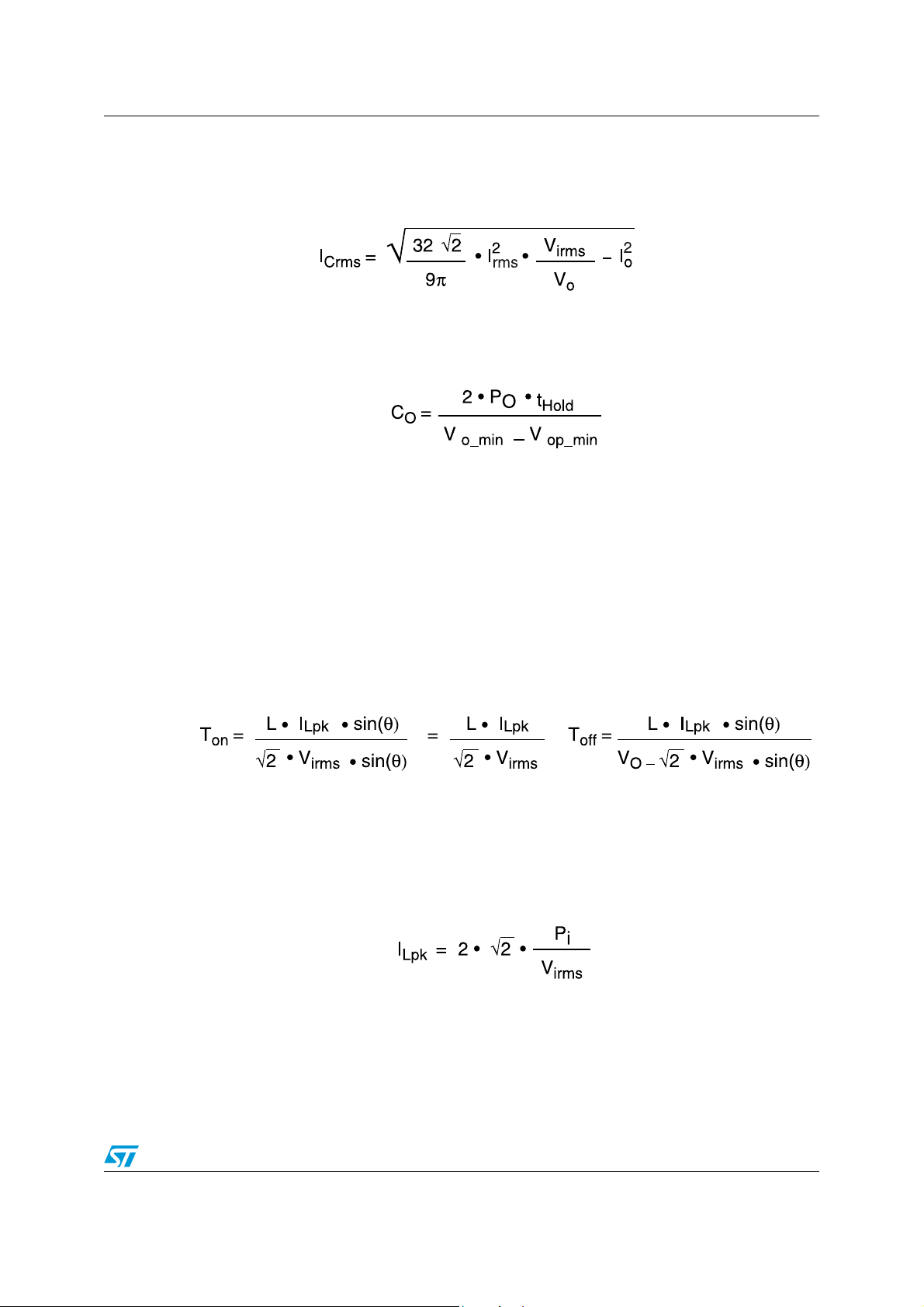
A.1 Input capacitor
The input high frequency filter capacitor (C3) has to attenuate the switching noise due to the
high frequency inductor current ripple (twice the average line current, Figure 9). The worst
conditions occur on the peak of the minimum rated input voltage. The maximum high
frequency voltage ripple is usually imposed between 1% and 10% of the minimum rated
input voltage. This is expressed by a coefficient ‘r’ (typically , r = 0.01 to 0.1):
High values of C
alleviate the burden to the EMI filter but cause the power factor and the
3
harmonic contents of the mains current to worsen, especially at high line and light load. On
the other hand, low values of C
but require heavier EMI filtering and increase power dissipation in the input bridge. It is up to
the designer to find the right trade-off in their application.
A.2 Output capacitor
The output bulk capacitor (Co) selection depends on:
● the DC output voltage;
● the adm itted overvoltage;
● the outp ut power ;
● the des ired voltage ripple.
A voltage ripple (∆Vo = 1/2 ripple peak-to-peak value) of 100 to 120Hz (twice the mains
frequency) is a function of the capacitor impedance and the peak capacitor current (I
Io):
With a low ESR capacitor the capacitive reactance is dominant, therefore:
improve power fact or and reduce mains current distortion
3
C(2f)pk
=
28/35
Page 29
AN2459 - Application note Components calculation
∆Vo is usually selected in the range 1 to 5% of the output voltage. Although ESR usually
does not affect the output ripple, it has to be taken into account for power loss calculations.
The total RMS capacitor ripple current, including mains frequency and switching frequency
components, is:
If the application has to guarantee a specified hold-up time, the selection criterion of the
capacitance will change: C
has to deliver the output power for a certain time (t
o
Hold
) with a
specified maximum dropout voltage:
22
where V
is the minimum output voltage value (which takes load regulation and output
o_min
ripple into account) and V
fail' detection from the downstream system supplied by the PFC.
A.3 Boost inductor
Designing the boost inductor involves several parameters and different approaches can be
followed. First, the inductance value must be defined. The inductance (L) is usually
determined so that the minimum switching frequency is greater than the maximum
frequency of the internal start er, to ensure a correct TM operation. Assuming unity PF, it is
possible to write:
T
being the ON-time and T
on
inductor current in a line cycle and θ the instantaneous line phase (θ
ON-time is constant over a line cycle.
As previously mentioned, I
the input power and the line voltage:
is the minimum output operating voltage before the 'power
op_min
the OFF-time of the power MOSFET, I
off
the maximum peak
Lpk
∈ (0,π)). Note that the
is twice the line-frequency peak current, which is related to
Lpk
29/35
Page 30

Components calculation AN2459 - Application note
Substituting this relationship in the expressions of Ton and T
possible to find the instantaneous switching frequency along a line cycle:
The switching frequency will be minimum at the top of the sinusoid (θ =
maximum at the zero crossings of the line voltage (θ = 0 or
The absolute minimum frequency f
mains voltage, thus the inductor value is defined by:
where V
Once the value of L is defined, the real design of the inductor can start. Standard high
frequency ferrite (gapped core-set with bobbin) is the usual choice in PFC applications.
Selection of the most suitable one, among the various types offered by manufacturers, will
depend on technical and economic considerations.
The next step is to estimate the core size. To calculate an approximate value of the minimum
core size, the following practical equation may be used:
can be either V
irms
irms(min)
can occur at either the maximum or the minimum
sw(min)
or V
irms(max
), whichever gives the lower value for L.
, after some algebra it is
off
π/2 ⇒
sin(θ) =1 ),
π ⇒
sin (θ) = 0) where T
off
= 0.
•
I
2
rms
I
e
gap
1
e
2
Volume ≥ 4K • L • I
3
where Volume is expressed in cm
the ratio of the gap length (l
The ratio l
Next, the winding has to be specified. Quantities to be defined include the turn number and
the wire cross-section.
The (maximum) instantaneous energy inside the boost inductor (1/2 × L × ILpk^2) can be
expressed in terms of energy stored in the magnetic field, given by the maximum energy
density times and the effective core volum e V
is fixed by t he designer.
e/lgap
1
• L • I
gap
2
Lpk
2
where: A
field strength and ∆B is the swing of the magnetic flux density.
is the effective area of the core cross-section, ∆H is the swing of the magnetic
e
, L in mH and the specific energy constant K depends on
) and the effective m agnet ic length (le) of the ferrite core:
K ≅ 14 • 10
–3
:
e
1
= • ∆H • ∆B • Ve ≈ • ∆H • ∆B • Ae• I
2
30/35
Page 31

AN2459 - Application note Components calculation
An air gap needs to be introduced to prevent the core from saturating because of its high
permeability and to allow an adequate ∆H.
Despite the fact that gap length l
so high (for power ferrites the typical value of µ
good approximation (∆H » ∆Hgap), that the whole magnetic field is concentrated in the air
gap. For instance, with an l
error caused by the above assumption is approximately 4%. The error is smaller if the l
ratio is larger. As a result, the fringing flux in the air gap region may be negl ec ted and the
energy balance can be re-written as:
gap/le
L • I
The flux density ∆B, is the same throughout the core and the air gap, and is related to the
field strength inside the air gap by the well-known relationship:
Then, taking Ampere's law into account (but applying it only to the air gap region):
it is possible to obtain the fol lowing equation from the energy balance equation :
is only a small per cent of le, the permeability of ferrite is
gap
value of 1% (which is the minimum suggested value) the
2
≈ ∆H
Lpk
∆Β
I
• ∆H
gap
is 2500) that it is possible to assume, with
r
• ∆B • Ae• I
gap
=
µ0 • ∆H
gap
gap
≈ N • I
gap
Lpk
gap/le
where N is the turn number of the winding.
Because N is defined, it is recommended to check the core saturation. If the core saturation
result is too close to the rated limit, it wi ll be necessa ry to increase the value of l
make a new calculation.
The wire gauge selection is based on limiting the copper losses to an acceptable value:
4
PCU = • I
2
rms
• RCU
gap
and
3
Due to the high ripple frequency, the effective wire resistance R
proximity effects . For this reason litz wire or multi-wire solutions are recommended. Finally,
the space occupied by the winding needs to be evaluated. If it does not fit the winding area
of the bobbin, a bigger core set needs to be considered and the winding calculation
repeated. It is also necessary to add an auxiliary winding to the inductor, in order for the
ZCD pin to recognize at what point the current flowing through the inductor has fallen to
zero. The winding is a low cost thin wire and the turn number is the only parameter to be
defined.
increase s by s kin and
CU,
31/35
Page 32

Components calculation AN2459 - Application note
A.4 Power MOSFET
The choice of MOSFET mainly concerns the R
The breakdown voltage is fixed by sum of the output voltage, the overvoltage and a safety
margin .
The MOSFET's power dissipation depends on conduction and switching losses.
The conduction losses are given by:
= I
=
V
2
Qrms
O
P
ON
where:
Switching losses due to current-voltage cross occur only at turn-off because of the TM
operation:
P
CROSS
where t
drain capacitance inside the MOSFET itself. In general, these losses are given by:
is the crossover time at turn-off. At turn-on, loss is due to the discharge of the total
fall
, which depends on the output power.
DSon
• R
DSon
•
I
• t
fall
• f
sw
rms
P
CAP =
3.3 • C
(
OSS
1.5 2
• V
DRAIN +
1
• C
d
• V
DRAIN
)
• f
sw
2
where C
external drain parasitic capacitance and V
practice, it is possible to give only a rough estimate of the total switc hi ng losses because
both f
not only by the sinusoidal change of the input voltage but also by the drop due to the
resonance of the boost inductor with the total drain capacitance. At low mains voltage, this
causes V
show that "Zero-Voltage-Switchin g" occurs as long as the instantaneous line voltage is less
than half the output voltage.
is the internal drain capacitance of the MOSFET (at VDS = 25V), Cd is the total
and V
sw
oss
change along a given line half-cycle. V
DRAIN
to be zero during a significant portion of each line half-cycle. It is possible to
DRAIN
is the drain voltage at MOSFET turn-on. In
DRAIN
, in particular, is affected
DRAIN
32/35
Page 33

AN2459 - Application note Components calculation
A.5 Boost Diode
The boost freewheeling diode is a fast recovery one. Its respective DC and RMS current
values, which are useful for loss computations, are given below:
The conduction losses can be estimated as follows:
P
DON
= V
• IDO + Rd • I
to
2
Drms
where V
The breakdown voltage is fixed with the same criterion as the MOSFET.
(threshold voltage) and Rd (differential resistance) are parameters of the diode.
to
33/35
Page 34

Revision history AN2459 - Application note
7 Revision history
Table 4. Document revision history
Date Revision Changes
17-Jan-2007 1 Initial release.
34/35
Page 35

AN2459 - Application note
y
y
Please Read Caref u lly:
Information in this document is provided solely in connection with ST products. STMicroelectronics NV and its subsidiaries (“ST”) reserve the
right to make changes, corrections, modifications or improvements, to this document, and the products and services described herein at an
time, with out notice.
All ST products are sold pursuant to ST’s terms and conditions of sale.
Purchase rs are solely responsible for the choice, selection and use of the S T products and serv i ces descri bed herein , and ST assumes no
liability whatsoever relating to the choice, selection or use of the ST products and services described herein.
No license, express or implied, by estoppel or otherwise, to any intellectual property rights is granted under this document. If any part of this
document refers to any third party products or services i t s hall not be d eem ed a license grant by ST for the use of such thi rd party p roducts
or services , or any intel lec tual pro per ty cont aine d ther ein or con sidere d as a warra nty c overi ng th e use i n any mann er w hats oever of such
third party products or s ervices or any i ntellectual property contained therein.
UNLESS OTHERWISE SET FORTH IN ST’S TERMS AND CONDITIONS OF SALE ST DISCLAIMS ANY EXPRESS OR IMPLIED
WARRANTY WITH RESPECT TO THE USE AND/OR SALE OF ST PRODUCTS INCLUDING WITHOUT LIMITATION IMPLIED
WARRANTIES OF MERCHANTABILITY, FITNESS FOR A PARTICULAR PURPO SE (AND THEIR EQUIVALENTS UNDER THE LAWS
OF ANY JURISDICTION), OR INFRINGEMENT OF ANY PATENT, COPYRIGHT OR OTHER INTELLECTUA L PROPERTY RIGHT.
UNLESS EXPRESSLY APPROVED IN WRITING BY AN AUTHORIZED ST REPRESENTATIVE, ST PRODUCTS ARE NOT
RECOMM ENDE D, AUTH ORI ZED OR WARR ANT ED FOR U SE IN MIL ITA RY, AIR CR AFT, SPA CE, LIF E SAV ING, OR LI FE S USTA INI NG
APPLICATIONS, NOR IN PRODUCTS OR SYSTEMS WHERE FAILURE OR MALFUNCTION MAY RESULT IN PERSONAL INJURY,
DEATH, OR SEVERE PROPERTY OR ENVIRONMENTAL DAMA G E. S T PR ODUC TS W HIC H ARE NOT SPECIFIED AS "AUTOMOTIVE
GRADE" MAY ONLY BE USED IN AUTOMOTIVE APPLICATIONS AT USER’S OWN RISK.
Resale of ST products with provisions different from the statements and/or technical features set forth in this document shall immediately void
any warran ty gr anted by ST fo r the ST produc t or se rvice d es cribed he rein and shall not c reat e o r extend in a ny mann er wha tsoe ver, an
liability of ST.
ST and the ST logo are trademarks or regis t ered trademarks of ST in vari ous countries.
Information in this docum ent supersedes and replaces all information previously supplied.
The ST logo is a registered trademark of STMicroelectronics. All other names are the property of their respective owners.
© 2007 STMi croelectro ni cs - All rights reserved
STMicroelectron ics group of com panies
Austra l i a - Be l gi um - Brazil - Canada - China - Czech Rep ubl i c - Finland - France - Germ any - Hong Kon g - India - Israe l - It aly - Japan -
Malaysi a - M al ta - Morocco - Singapore - Spain - Sweden - Switze rl and - United Kingdom - Unit ed States of America
www.st.com
35/35
 Loading...