

Page 1

AN2442
Application note
Using the STR91xFA DMA controller
Introduction
This application note provides information on how to use and take full advantage of the
STR91xFA DMA controller. It is intended for anyone getting started with DMA.
While it is impossible to cover every possible control scenario of each peripheral DMA
transfer, those considered to be the most typical and useful are described.
Software is available with this application note and can be downloaded separately from
www.st.com.
June 2008 Rev 2 1/22
www.st.com
Page 2

Contents AN2442
Contents
1 DMA unit . . . . . . . . . . . . . . . . . . . . . . . . . . . . . . . . . . . . . . . . . . . . . . . . . . . 4
1.1 DMA features . . . . . . . . . . . . . . . . . . . . . . . . . . . . . . . . . . . . . . . . . . . . . . . 4
1.2 Peripheral DMA support . . . . . . . . . . . . . . . . . . . . . . . . . . . . . . . . . . . . . . . 5
1.3 DMA request signals . . . . . . . . . . . . . . . . . . . . . . . . . . . . . . . . . . . . . . . . . 6
1.4 DMA transfer properties . . . . . . . . . . . . . . . . . . . . . . . . . . . . . . . . . . . . . . . 7
1.4.1 DMA channel . . . . . . . . . . . . . . . . . . . . . . . . . . . . . . . . . . . . . . . . . . . . . . 7
1.4.2 Source and destination addresses . . . . . . . . . . . . . . . . . . . . . . . . . . . . . 7
1.4.3 Source and destination data width . . . . . . . . . . . . . . . . . . . . . . . . . . . . . . 7
1.4.4 Flow control . . . . . . . . . . . . . . . . . . . . . . . . . . . . . . . . . . . . . . . . . . . . . . . 7
1.4.5 Transfer type . . . . . . . . . . . . . . . . . . . . . . . . . . . . . . . . . . . . . . . . . . . . . . 8
1.4.6 Transfer size . . . . . . . . . . . . . . . . . . . . . . . . . . . . . . . . . . . . . . . . . . . . . . . 8
1.4.7 Source and destination burst size . . . . . . . . . . . . . . . . . . . . . . . . . . . . . . 8
1.4.8 Incrementing source/destination address . . . . . . . . . . . . . . . . . . . . . . . . 8
1.4.9 Terminal count interrupt . . . . . . . . . . . . . . . . . . . . . . . . . . . . . . . . . . . . . . 9
1.4.10 DMA linked lists . . . . . . . . . . . . . . . . . . . . . . . . . . . . . . . . . . . . . . . . . . . 10
1.5 Programming the DMAC using the STR9 software library . . . . . . . . . . . . 12
2 DMA transfer examples . . . . . . . . . . . . . . . . . . . . . . . . . . . . . . . . . . . . . 14
2.1 Memory to memory transfer . . . . . . . . . . . . . . . . . . . . . . . . . . . . . . . . . . . 14
2.1.1 Transfer properties . . . . . . . . . . . . . . . . . . . . . . . . . . . . . . . . . . . . . . . . . 14
2.2 Memory to SPP transfer . . . . . . . . . . . . . . . . . . . . . . . . . . . . . . . . . . . . . . 14
2.2.1 SSP DMA interface overview . . . . . . . . . . . . . . . . . . . . . . . . . . . . . . . . . 14
2.2.2 Memory to SSP example . . . . . . . . . . . . . . . . . . . . . . . . . . . . . . . . . . . . 14
2.2.3 Transfer properties . . . . . . . . . . . . . . . . . . . . . . . . . . . . . . . . . . . . . . . . . 15
2.2.4 Hardware connection . . . . . . . . . . . . . . . . . . . . . . . . . . . . . . . . . . . . . . . 15
2.3 UART to memory transfer . . . . . . . . . . . . . . . . . . . . . . . . . . . . . . . . . . . . . 15
2.3.1 UART-Rx DMA interface . . . . . . . . . . . . . . . . . . . . . . . . . . . . . . . . . . . . . 15
2.3.2 UART to memory example . . . . . . . . . . . . . . . . . . . . . . . . . . . . . . . . . . . 16
2.3.3 Transfer properties . . . . . . . . . . . . . . . . . . . . . . . . . . . . . . . . . . . . . . . . . 16
2.3.4 Hardware connection . . . . . . . . . . . . . . . . . . . . . . . . . . . . . . . . . . . . . . . 16
2.4 Memory to UART transfer . . . . . . . . . . . . . . . . . . . . . . . . . . . . . . . . . . . . . 16
2.4.1 UART-TX DMA interface . . . . . . . . . . . . . . . . . . . . . . . . . . . . . . . . . . . . 16
2.4.2 Memory to UART example . . . . . . . . . . . . . . . . . . . . . . . . . . . . . . . . . . . 16
2/22
Page 3

AN2442 Contents
2.4.3 Transfer properties . . . . . . . . . . . . . . . . . . . . . . . . . . . . . . . . . . . . . . . . . 17
2.4.4 Use of linked lists for DMA transfer . . . . . . . . . . . . . . . . . . . . . . . . . . . . 17
2.4.5 Terminal count interrupt generation . . . . . . . . . . . . . . . . . . . . . . . . . . . . 17
2.5 DMA transfer triggered by external DMA request . . . . . . . . . . . . . . . . . . . 18
2.5.1 External request example . . . . . . . . . . . . . . . . . . . . . . . . . . . . . . . . . . . 18
2.5.2 Transfer properties . . . . . . . . . . . . . . . . . . . . . . . . . . . . . . . . . . . . . . . . . 18
2.6 Timer to memory transfer . . . . . . . . . . . . . . . . . . . . . . . . . . . . . . . . . . . . . 18
2.6.1 Timer DMA interface overview . . . . . . . . . . . . . . . . . . . . . . . . . . . . . . . . 18
2.6.2 Timer to memory example . . . . . . . . . . . . . . . . . . . . . . . . . . . . . . . . . . . 18
2.6.3 Transfer properties . . . . . . . . . . . . . . . . . . . . . . . . . . . . . . . . . . . . . . . . . 19
2.6.4 Use of linked lists for DMA transfer . . . . . . . . . . . . . . . . . . . . . . . . . . . . 19
2.6.5 Hardware connection . . . . . . . . . . . . . . . . . . . . . . . . . . . . . . . . . . . . . . . 20
3 Revision history . . . . . . . . . . . . . . . . . . . . . . . . . . . . . . . . . . . . . . . . . . . 21
3/22
Page 4

DMA unit AN2442
1 DMA unit
The STR91xFA DMA controller (DMAC) is an AMBA AHB module, and connects to the
Advanced High-performance Bus (AHB). It allows devices to transfer data to or from the
system's memory and registers without the intervention of the CPU. While the transfer takes
place the CPU is free to do other things. As a result, the STR9 core is not overloaded to
serve all peripherals and there is an overall speed-up in CPU operation chiefly when
transferring a large amount of data.
1.1 DMA features
The DMAC offers:
● Eight DMA channels. Each channel can support a unidirectional transfer.
● Hardware DMA channel priority. Each DMA channel has a specific hardware priority.
DMA channel 0 has the highest priority and channel 7 has the lowest. If requests from
two channels become active at the same time, the channel with the highest priority is
serviced first.
● The DMAC provides 14 peripheral DMA request lines (refer to Table 1.).
● Single DMA and burst DMA request signals. Each peripheral connected to the DMAC
can assert either a burst DMA request or a single DMA request. Note that peripherals
without FIFO inside can not generate a DMA burst request.
● Programmable DMA burst size. The DMA burst size can be programmed to transfer
data more efficiently. Therefore, up to 256 data per block can be reached (note that the
data width can be configured to byte, half-word or word).
● Support for memory-to-memory, memory-to-peripheral, peripheral-to-memory, and
peripheral-to-peripheral transfers.
● Incrementing or non-incrementing addressing for source and destination.
● DMA Linked list support: the DMAC is able to perform a chained list of DMA transfers
without need for CPU intervention
● Separate and combined DMA error and DMA Terminal Count interrupt requests: An
interrupt can be generated to the processor on a DMA error or when a DMA count has
reached 0 (Terminal Count event, usually used to indicate that a transfer has finished).
4/22
Page 5
AN2442 DMA unit
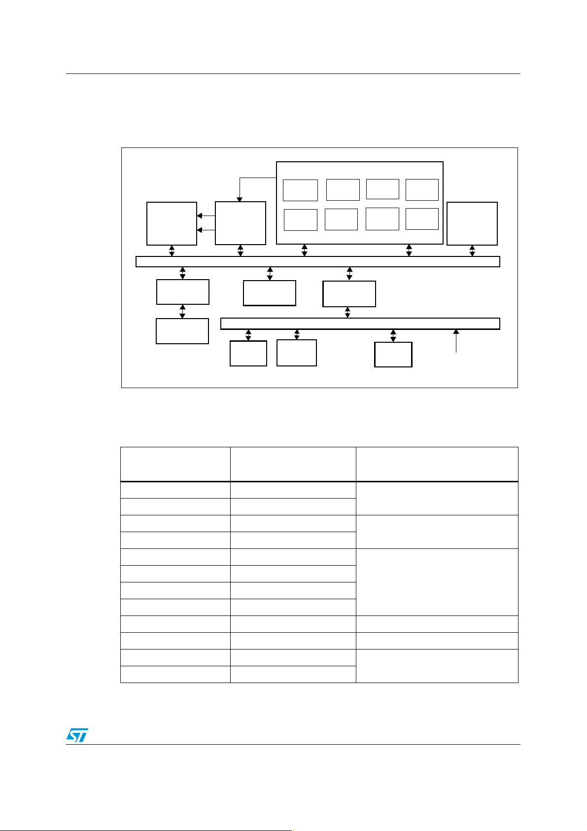
ARM Core
USB
VIC
EMI
APB
External
TIM0SSP0 UART0
Bridge
SSP1 UART1 TIM1
Memory
Channel7
2xExternal DMA Requests 1)
AHB Bus
APB Bus
RAM
IRQ
FIQ
FIFO
Channel6 Channel5
Channel2Channel3 Channel1
Channel4
Channel0
FIFO FIFO FIFO
FIFO FIFO FIFO FIFO
DMA Interrupt Request
DMA Controller
DMA Request0:Pin 3.0
DMA Request1:Pin 3.1
1.2 Peripheral DMA support
Peripherals supporting the DMA are shown in this block diagram:
Figure 1. DMAC and peripherals with DMA support
Note: 1 An external DMA request can be generated from 2 GPIO pins going to high levels.
The DMAC requests and triggering events are summarized in the following table:
Table 1. STR91x DMA requests
DMA request signal
0 USB RX
1 USB TX
2TIM0
3TIM1
4UART0 RX
5UART0 TX
6UART1RX
7 UART1TX
8 External DMA Req0 Rising edge of P3.0
9 External DMA Req1 Rising edge of P3.1
10 -
11 -
Associated peripheral
function
DMA trigger
USB correct transfer event
Input Capture and Output Compare
events
FIFO watermark level reached
Reserved
5/22
Page 6
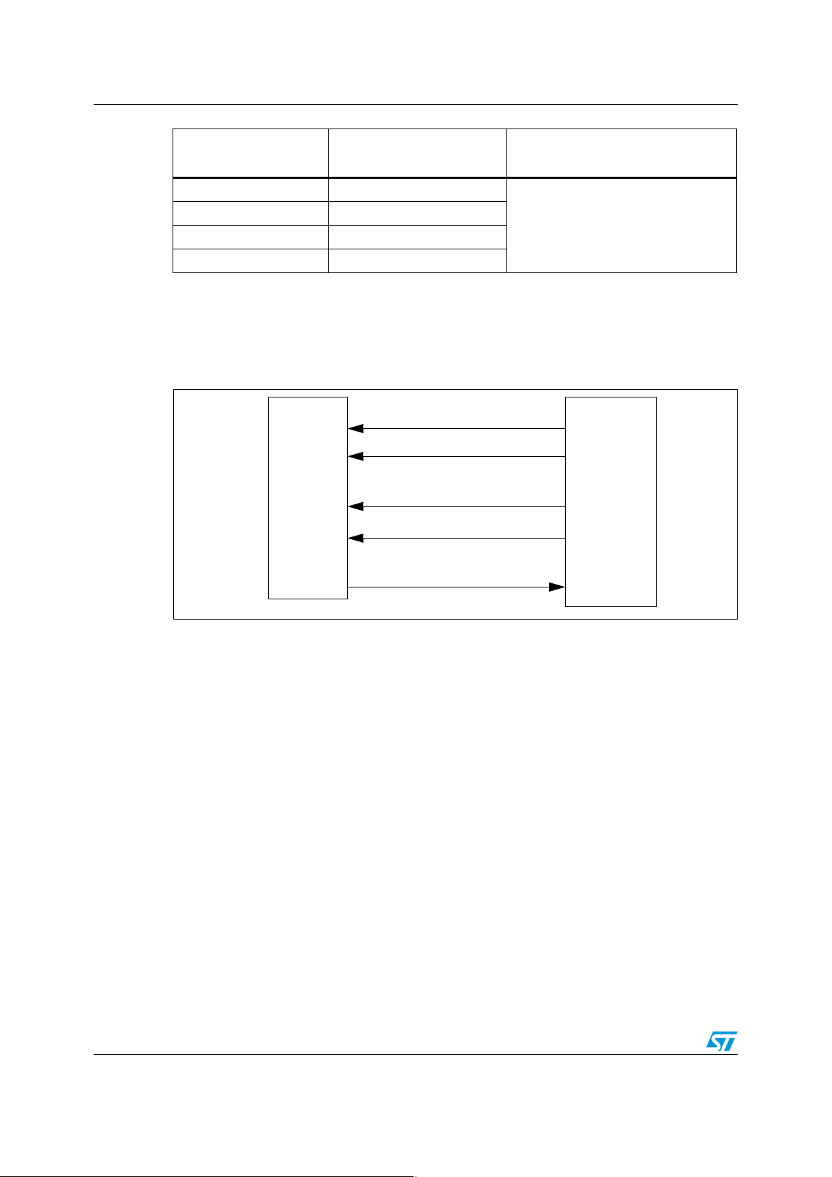
DMA unit AN2442
DMAC
Peripheral
Single DMA request
1)
Burst DMA request
Last single DMA request
3)
Last burst DMA request
3)
DMA request clear
4)
2)
DMA request signal
12 SSP0 RX
13 SSP0TX
14 SSP1RX
15 SSP1 TX
Associated peripheral
1.3 DMA request signals
The following figure describes the signals used for peripherals to request a DMA transfer:
Figure 2. DMA request signals
function
DMA trigger
Half FIFO level reached
1. Single DMA requests are asserted when the peripheral has to transfer one data item.
2. Burst DMA requests are asserted when the peripheral has multiple data items to
transfer. Note that the single and burst requests are not mutually exclusive, they could
be asserted together by the peripheral.
3. Last burst and last single requests can be asserted only when the peripheral is the flow
controller in order to indicate the last transfer request to the DMAC (in STR91xFA, only
the USB has these signals).
4. DMA request clear is asserted by the DMAC to indicate to peripheral that the request
has been serviced.
6/22
Page 7

AN2442 DMA unit
1.4 DMA transfer properties
A DMA transfer is characterized by the following properties:
● DMA Channel
● Source and destination addresses
● Source and destination data width
● Flow control
● Transfer type
● Transfer size (only when DMAC is the flow controller)
● Source / destination burst size
● Source / destination address incrementing or non-incrementing
● Terminal count interrupt generation
● Next linked list item address
In the following paragraphs, a detailed description of each DMA transfer property is provided.
1.4.1 DMA channel
A DMA channel needs to be allocated by the user (8 channels are available) for the DMA
request. The choice of the channel depends on the required priority (0 to 7) and on the
availability of the channel (not already allocated to another request).
1.4.2 Source and destination addresses
A DMA transfer is defined by a source address and a destination address. Both the source and
destination should be in the AHB or APB memory ranges.
1.4.3 Source and destination data width
Data width for source and destination can be defined as:
● Byte
● Half word (16-bit)
● Word (32-bits)
1.4.4 Flow control
The flow controller is the unit that controls the data transfer length and which is responsible for
stopping the DMA transfer.
The flow controller can be either the DMAC or the peripheral.
● With DMAC as flow controller:
In this case, it is necessary to define the transfer size value.
When a DMA request is served, the transfer size value decreases by the amount of
transferred data (depending of the type of request: burst or single).
When the transfer size value reaches 0, the DMA transfer is then finished and the DMA
channel is disabled in case of no next linked list item, otherwise a new linked list descriptor
will be fetched from SRAM into DMA registers.
For further details about linked lists, refer to Section 1.4.10.
● With the peripheral as flow controller:
7/22
Page 8

DMA unit AN2442
In this case, the transfer size value is ignored.
In fact, it is up to the peripheral to signal the end of transfer by using Last Burst or Last
single request lines.
In the STR91xFA, only the USB peripheral supports these two signals (Last Burst and
Last single requests). For other peripherals when used as flow controller, peripheral
interrupts can be used to stop a transfer, by halting the DMA channel.
1.4.5 Transfer type
The transfer type could be:
● Memory to memory
● Memory to peripheral
● Peripheral to memory
● Peripheral to peripheral
Note: 1 In memory to memory transactions, the DMAC should be the flow controller and DMA
transfer is started without any request.
2 In memory to peripheral transactions under DMAC flow controller only the DMA burst
requests are monitored by the DMAC.
1.4.6 Transfer size
As described in Section 1.4.4, the transfer size value has to be defined only when the DMAC
is the flow controller, in fact this value defines the number of data to be transferred from
source to destination.
Depending on the received request: burst or single, the transfer size value is decreased by
the amount of transferred data.
1.4.7 Source and destination burst size
For burst transfers (when supported), it is necessary to define the burst size value. This
value defines how much data is to be transferred when a burst request is received.
Depending on the type of the transfer, the following need to be defined:
● The source burst size when doing a peripheral to memory transfer
● The destination burst size when doing a memory to peripheral transfer
Note: If the DMAC is the flow controller and burst size value is not 0, then two cases are possible:
– Current Transfer size value is greater than burst size value. In this case the DMAC will
monitor and serve only the burst requests.
– Current Transfer size value is less than burst size value. In this case the DMAC will
monitor single DMA requests until the transfer size value reaches 0. An exception to
this is when the transfer is from memory to peripheral, in this case only burst requests
will continue to be monitored.
1.4.8 Incrementing source/destination address
It is possible to configure the DMAC to automatically increment the source or/and
destination address after each data transfer.
8/22
Page 9

AN2442 DMA unit
a
b
c
d
e
...
a
b
Source address
Destination address
Incrementing source
Incrementing destination
DMA data transfer
Figure 3. DMA source address & destination address incrementing
1.4.9 Terminal count interrupt
The DMAC can be configured to generate an interrupt: “the terminal count interrupt” at the
end of the DMA transfer.
Also when using linked lists, a terminal count interrupt can be generated at the end of each
linked list transfer.
9/22
Page 10
DMA unit AN2442
DMAC registers SRAM
1st DMA
Transfer
2nd DMA
Transfer
Descriptor
3rd DMA
Transfer
Descriptor
Last DMA
Transfer
Descriptor
Null
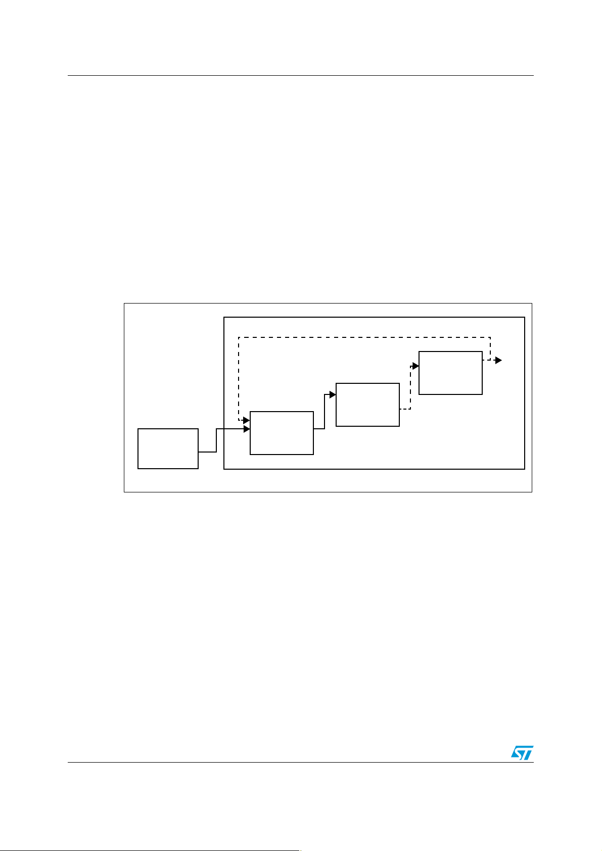
1.4.10 DMA linked lists
DMA linked lists are used in order to perform a set of DMA transfers without need for CPU
intervention.
The first DMA transfer properties should be programmed in the DMAC registers. The next
transfers properties are stored in SRAM as “descriptors”.
Each DMA descriptor has a pointer to the next linked list item.
The last linked list item points to Null or can point the first (or other) descriptor in order to
form a chained linked list.
After finishing a transfer, the DMA will automatically fetch the next linked list descriptor from
memory in order to perform the next transfer.
When finishing the last linked list transfer and there is no next descriptor to fetch, the DMA
channel will be disabled.
Figure 4. Linked lists
As explained above, in order to use linked lists, the first transfer parameters must be
programmed in the DMA registers. This configuration should include the address of the first
linked list item in SRAM.
The SRAM descriptors must then be programmed. These are in the form of a structure with
the following four 32-bit words organized as follows:
● Source address
● Destination address
● Pointer to next LLI (Linked List Item)
● Control word: This 32-bit word has the same bit fields as the DMA_ChannelControl
register DMA_CC.
10/22
Page 11

AN2442 DMA unit
1st Block
2nd Block
3rd Block
1st Block
2nd Block
3rd Block
Source address 1
Source address 2
Source address 3
Destination address 1
Destination address 2
Destination address 3
Source address 1
Destination address 1
Pointer to next LLI1
Channel Control word 1
Source address 2
Destination address 2
Pointer to Next LLI2
Channel Control word 2
Source address 3
Destination address 3
Pointer to next LLI3
Channel Control word 3
Null
Use of linked lists
DMAC registers SRAM
An example use of DMA linked list is the “scattering” of contiguous blocks into different areas
in memory.
Figure 5. Example use of DMA linked lists
As shown in figure above, the DMA linked lists are used in order to transfer 3 data blocks to
three different areas in memory.
The first block transfer is done using the first descriptor programmed in DMA registers, and
the 2nd and 3rd transfers are done using linked list descriptors in SRAM.
Depending on the “Channel Control word” TCIE bit (see DMA_CC register), the user can
choose to generate or not a Terminal Count interrupt at the end of each linked list transfer.
11/22
Page 12

DMA unit AN2442
1.5 Programming the DMAC using the STR9 software library
Some software considerations must be taken into account when programming the DMAC,
(Refer to section 9.4 in the STR91xFA Reference Manual).
The STR91xFA software library DMAC driver provides an easy way to configure the DMAC
registers.
In order to configure the DMA transfer properties for a DMA channel, the following structure
needs to be used:
Typedef struct
{
u32 DMA_Channel_SrcAdd; /* DMA transfer source address */
u32 DMA_Channel_DesAdd; /* DMA transfer destination address */
u32 DMA_Channel_LLstItm; /* DMA next linked list address */
u8 DMA_Channel_DesWidth; /* Destination data width */
u8 DMA_Channel_SrcWidth; /* Source data witdh */
u8 DMA_Channel_DesBstSize; /* Destination Burst size */
u8 DMA_Channel_SrcBstSize; /* Source Burst size */
u16 DMA_Channel_TrsfSize; /* Transfer size value */
u8 DMA_Channel_FlowCntrl; /* Flow controler & transfer type */
u8 DMA_Channel_Src; /* DMA request source */
u8 DMA_Channel_Des; /* DMA request destination */
} DMA_InitTypeDef;
The following explains the required steps to program the DMAC:
1. Enable the DMAC clock and exit it from Reset state
2. Enable the DMAC:
DMA_Cmd(ENABLE);
3. Fill a structure of type DMA_InitTypeDef with the correct configuration parameters:
DMA_struct.DMA_Channel_SrcAdd = .. ;
DMA_struct.DMA_Channel_DesAdd = .. ;
DMA_struct.DMA_Channel_LLstItm = .. ;
DMA_struct.DMA_Channel_DesWidth = .. ;
DMA_struct.DMA_Channel_SrcWidth = .. ;
DMA_struct.DMA_Channel_SrcBstSize = .. ;
DMA_struct.DMA_Channel_TrsfSize = .. ;
DMA_struct.DMA_Channel_FlowCntrl= .. ;
DMA_struct.DMA_Channel_Src = .. ;
4. Choose and free DMA channel with the required priority. DMA channel 0 has the
highest priority and DMA channel 7 the lowest priority and update DMAC registers:
DMA_Init(DMA_Channelx,&DMA_struct);
5. Use incrementing or non-incrementing addressing depending on source and
destination region:
DMA_ChannelSRCIncConfig (DMA_Channelx, ENABLE);
DMA_ChannelDESIncConfig (DMA_Channelx, ENABLE);
6. Enable DMAC channel:
DMA_ChannelCmd (DMA_Channelx,ENABLE);
12/22
Page 13

AN2442 DMA unit
/******************* Example DMA Config ***********************/
/* No next linked list item*/
DMA_struct.DMA_Channel_LLstItm= 0;
/* Source address of the DMA transfer */
DMA_struct.DMA_Channel_SrcAdd=(u32)(&TxBuffer0[0]);
/* Destination address of DMA the transfer is UART Data reg*/
DMA_struct.DMA_Channel_DesAdd=(u32)(&UART0->DR);
/* Source data width is Byte */
DMA_struct.DMA_Channel_SrcWidth= DMA_SrcWidth_Byte;
/* Destination bus width is Byte */
DMA_struct.DMA_Channel_DesWidth= DMA_DesWidth_Byte;
/* DMAC is The flow controller*/
DMA_struct.DMA_Channel_FlowCntrl=DMA_FlowCntrl1_DMA;
/*The DMAC is triggered by the SSP_DMA_Transmit request.*/
DMA_struct.DMA_Channel_Des= DMA_DES_UART0_TX;
/*Transfer size of 12 data */
DMA_struct.DMA_Channel_TrsfSize =12;
/* Update the DMA channel0 registers with DMA_struct values */
DMA_Init(DMA_Channel0,&DMA_struct);
/* Enable Source increment */
DMA_ChannelSRCIncConfig (DMA_Channel0, ENABLE);
/*Enable the Terminal Count interrupt*/
DMA_ITConfig(DMA_Channel0, ENABLE);
DMA_ITMaskConfig(DMA_Channel0, DMA_ITMask_ITC, ENABLE);
/*Enable the DMA channel0*/
DMA_ChannelCmd (DMA_Channel0,ENABLE);
7. A DMA terminal count interrupt or a DMA error interrupt can be generated:
DMA_ITConfig(DMA_Channelx, ENABLE);
DMA_ITMaskConfig(DMA_Channelx, DMA_ITMask_ITC, ENABLE);/* TC int */
DMA_ITMaskConfig(DMA_Channelx, DMA_ITMask_IE, ENABLE);/*Error int*/
The following part of the code example shows how to configure the UART-TX DMA interface
on channel0 with interrupt generation when DMA count reach 0.
13/22
Page 14

DMA transfer examples AN2442
2 DMA transfer examples
2.1 Memory to memory transfer
This example shows how to program a DMA channel for memory-to-memory transfers.
When enabled, the DMA channel starts to transfer data from the source buffer to the
destination buffer.
The DMA transfer starts just after enabling the DMAC without any DMA request. When the
transfer is finished, the DMA terminal count interrupt is generated.
2.1.1 Transfer properties
In this example:
● The DMAC is the flow controller.
● Burst DMA transfers are used.
● DMA source and destination incrementing are used
2.2 Memory to SPP transfer
2.2.1 SSP DMA interface overview
A programmable DMA channel may be assigned by CPU firmware to service each SSP unit
for fast and direct transfers between the SSP and SRAM with little CPU involvement. Both
DMA single-transfers and DMA burst-transfers are supported for transmit and receive.
During data reception by SSP, single DMA transfer request are asserted when the receive
FIFO contains at least one character. Burst DMA transfer request asserted by the SSP
when the receive FIFO contains four or more character.
During data transmission single DMA transfer requests are asserted when there is at least
one empty location in the transmit FIFO. Burst DMA transfer requests are asserted by the
SSP when the transmit FIFO contains four or less characters.
2.2.2 Memory to SSP example
This example described communication between two SSPs: SPP0 and SSP1.
SSP0 is configured as master and SSP1 as slave. The Motorola frame format “SPI” is the
used protocol for communication.
1. “SSP0_Buffer_Tx" buffer has to be transferred from SPP0 (master) to SSP1 (slave).
2. Data is received by SSP1 peripheral and stored in the SSP1_Buffer_Rx. A comparison
is then made with the expected values of the transmitted buffer. The result of this
comparison is returned in the "TransferStatus1" variable.
In this example the DMAC is used for transferring “SSP0_Buffer_Tx” data from SRAM to
SSP0 transmit FIFO.
14/22
Page 15

AN2442 DMA transfer examples
channel0
channel1
channel2
channel3
channel4
channel5
channel6
channel7
General registers
USB
TIMER
UART
External pins
SSP
DMA request signal
Acknowledge signal.
Channel Priority
Single/Burst
Burst Size
of 4 Bytes
When we reach
the water mark
level a DMA
request is
generated
RX-FIFO
DMA-Peripherals
DMA UNIT
2.2.3 Transfer properties
In this example:
● The flow controller is the DMAC.
● The DMAC is triggered by the SSP_DMA_Transmit request.
● No linked lists are used.
● Since the SSP has a FIFO, burst transfers can be used.
● Only the source address incrementing is used.
2.2.4 Hardware connection
To run this example, please connect both SSP0 and SSP1 pins as follows:
● Connect SSP0_SCLK(P2.4) to SSP1_SCLK(P3.4).
● Connect SSP0_MISO(P2.6) to SSP1_MISO(P3.5).
● Connect SSP0_MOSI(P2.5) to SSP1_MOSI(P3.6).
● Connect SSP0_nSS (P2.7) to VCC through a pull-up resistor.
● Connect SSP1_nSS (P3.7) to GND.
2.3 UART to memory transfer
A programmable DMA channel may be assigned by firmware to service channels UART0
and UART1 for fast and direct transfers between the UART and SRAM with little CPU
involvement.
2.3.1 UART-Rx DMA interface
The DMAC is triggered when the receive FIFO level reaches the defined watermark level.
The burst transfer and single transfer request signals are not mutually exclusive, they can
both be asserted at the same time. When there is more data than the watermark level in the
receive FIFO, the burst transfer request and the single transfer request are asserted (refer to
Figure 6). When the amount of data left in the receive FIFO is less than the watermark, only
the single request is asserted. This is useful for situations where the number of characters
left to be transferred in the stream is less than a burst.
Figure 6. DMA- UART-RX interface
15/22
Page 16

DMA transfer examples AN2442
2.3.2 UART to memory example
In this example data is transferred from a PC using the HyperTerminal application to the
UART0 receive FIFO.
UART0 waits for a string to be entered from HyperTerminal. Each byte tapped through this
utility is received by the UART0.
The data received in the UART-RX FIFO is transferred to SRAM “RxBuffer” using DMA.
Note: The received buffer has a maximum size of RxBufferSize (bytes).
2.3.3 Transfer properties
In this example:
● The flow controller is the DMAC.
● The transfer type is peripheral to memory.
● The DMAC transfer is triggered by the UART_DMA_Receive request.
● The burst size is 4 bytes.
● No DMA linked list are used.
● Only the destination address incrementing is used.
2.3.4 Hardware connection
Connect a null-modem RS232 cable between the DB9 connector of UART0 and PC serial
COM port.
2.4 Memory to UART transfer
2.4.1 UART-TX DMA interface
A single character DMA transfer request is asserted by the UART when there is at least one
empty location in the transmit FIFO. A burst DMA transfer request is asserted by the UART
when the transmit FIFO contains less characters than the watermark level.
The following examples provide a basic communication between UART0 and HyperTerminal
using DMA capability.
2.4.2 Memory to UART example
The DMA transfers data from TxBuffer0, TxBuffer1, TxBuffer2 to UART0 Tx FIFO. Each
source buffer has a fixed size. The transferred data can then be shown in the HyperTerminal
utility.
The CPU is applied to generate an interrupt after each amount of data to be transferred by
DMA.
16/22
Page 17

AN2442 DMA transfer examples
15 14 13 12 11 10
31 30 29 27 26 161718
5
25 24 23 22 21 20 19
9876 43210
TransferSize[11:0]
DB
rw
rwrwrwrwrwrwrw rw rw rw rw rw rw rw rw rw
rw
DBSize[2:1]SWIDTHDWID TH
rwrwrw rwrw rw rwrwrwrwrwrwrw rw
Size0
SBSize[2:0]
Reset Value:0000 0000h
TCIE
PROT PROT
2
1
DI SI 0
PROT
0
0
28
2.4.3 Transfer properties
In this example:
● The flow controller is DMAC.
● The transfer type is memory to peripheral.
● DMAC is triggered by the UART_DMA_Transmit request.
● Burst transfers are used and burst size is 4 bytes.
● Linked mode is used (see next section for details).
● Only the source address is incremented.
2.4.4 Use of linked lists for DMA transfer
In this example there are three different buffers which need to be transferred to a fixed
destination: the UART transmit FIFO.
This transfer can be done using the linked list:
● The first LLI (Linked List Item) is programmed into the DMAC registers and next
transfer linked lists are programmed as descriptors in SRAM.
● Each LLI controls the transfer of one block of data, and then optionally loads another
LLI to continue the DMA operation, or stops the DMA stream.
To determine the appropriate control information for each linked list item, refer to the
DMA_CCRx register bit fields:
Figure 7. DMA_CCRx register
2.4.5 Terminal count interrupt generation
To generate an interrupt request at each LLI termination, follow the procedure below:
● Enable the TC interrupt for each linked list by:
– Enabling TC interrupt for first transfer use DMA_ITConfig function
DMA_ITConfig (DMA_Channel1, ENABLE);
– Enabling this interrupt in the second and third linked list items: set bit “TCIE” in
each control word of the linked list descriptors (see Figure 7)
● Enable global TC interrupt for the current channel using DMA_ITMaskConfig function.
DMA_ITMaskConfig (DMA_Channel1, DMA_ITMask_ITC, ENABLE);
17/22
Page 18

DMA transfer examples AN2442
2.5 DMA transfer triggered by external DMA request
A DMA transfer can be triggered by an external pin:
● External DMA Req 0: When pin P3.0 goes high
● External DMA Req 1: When pin P3.1 goes high
Only one burst transfer is done after pin is driven to high state.
2.5.1 External request example
This example illustrates how to make a memory to memory DMA transfer (Buffer0 to
Buffer1) triggered by the External DMA Req 0.
A terminal count interrupt is generated at the end of the transfer.
The memory to memory transfer is triggered by pulling high pin P3.0
2.5.2 Transfer properties
In this example:
● The DMAC is the flow controller.
● The transfer type is memory to peripheral (even if the transfer is memory to memory, it
is necessary to set the transfer type to memory to peripheral).
● Burst transfer of 8 bytes is used: The particularity of the external request pin is to
generate only one burst request if the pin is driven to high state.
● No DMA linked lists are used.
● Source and destination address incrementing are used.
● Terminal count interrupt generation at the end of the transfer.
2.6 Timer to memory transfer
2.6.1 Timer DMA interface overview
A DMA interface is available on TIM0 and TIM1. The source can be selected to be IC1,
OC1, IC2 or OC2. The timer can perform DMA requests to a DMA module and then allow a
data transfer between STR9 resources using DMA.
For the timer peripheral there is no FIFO inside. So the IP can't generate a DMA burst
request to the DMA controller for burst transfer. Therefore the Timer need only a single
transfer to service the counter.
As a result, when the data path is from memory to Timer it is not possible to use the DMAC
as flow controller because the availability of DMA burst request is mandatory. This explains
why the Timer is used as flow controller in this case of transfer.
In the case of a data path from the Timer to memory, the DMA burst request is not
mandatory so either the DMAC or the Timer can be used as flow controller.
2.6.2 Timer to memory example
The following example shows how to use the TIM peripheral to measure the frequency and
the pulse width of an external signal.
18/22
Page 19

AN2442 DMA transfer examples
Period =
IC1R x t
PRESC
fPCLK
Pulse =
IC2R x t
PRESC
fPCLK
TIM0 is configured in PWM input mode. At each Input Capture1 event a transfer from
registers IC1R and IC2R to memory will occur.
To store ICR1 and ICR2 related to the same input capture event, use two channels;
channel0 to transfer the IC1R value and channel 1 to transfer the IC2R value.
A pattern can be used as the external signal to be sure that their pulse widths and periods
correspond with those stored in the memory.
TIM1 configured in PWM mode can generate such a pattern if its period and pulse width are
modified every output compare interrupt with the desired values.
To obtain the time values:
Where:
fPCLK = Internal clock frequency
tPRESC = Timer clock prescaler
2.6.3 Transfer properties
● The flow controller is DMAC.
● The transfer type: Peripheral to memory.
● DMAC is triggered by the Input capture1 event request.
● Burst transfers are not supported since there is no FIFO inside.
● Linked mode is used (see next section for details).
● Source and destination address not incremented.
2.6.4 Use of linked lists for DMA transfer
Linked lists is used due to the fact that the content of the two input capture registers
changes every time depending on the external signal. It is therefore possible to save these
values separately at each input capture event which gives more information about the
injected signal.
One linked list is used for each channel; link1 for channel0 and link2 for channel1. Therefore
linked list1 is used to transfer IC1R values to TIM-IC1R buffer and linked list2 to transfer
IC2R values to TIM-IC2R buffer (refer to Figure 8.).
19/22
Page 20

DMA transfer examples AN2442
IC1R
IC1R’
IC1R’’
IC2R
IC2R’
IC2R’’
TIM-IC1R Buffer
TIM-IC2R Buffer
Values transferred by
Values transferred by
DMA channel0
DMA channel1
IC1R
IC2R
,..,
,..,
values captured for the
same input capture event
Figure 8. Storage procedure of IC1R and IC2R registers
2.6.5 Hardware connection
The external signal comes from TM1-PWM pin to be injected in TM0-IC1 pin so:
● Connect TM1-PWM pin (P4.2) to TM0-IC1 pin (P4.0).
20/22
Page 21

AN2442 Revision history
3 Revision history
Table 2. Document revision history
Date Revision Changes
08-Jan-2007 1 Initial release.
02-Jun-2008 2 Removed I2C section.
21/22
Page 22

AN2442
Please Read Carefully:
Information in this document is provided solely in connection with ST products. STMicroelectronics NV and its subsidiaries (“ST”) reserve the
right to make changes, corrections, modifications or improvements, to this document, and the products and services described herein at any
time, without notice.
All ST products are sold pursuant to ST’s terms and conditions of sale.
Purchasers are solely responsible for the choice, selection and use of the ST products and services described herein, and ST assumes no
liability whatsoever relating to the choice, selection or use of the ST products and services described herein.
No license, express or implied, by estoppel or otherwise, to any intellectual property rights is granted under this document. If any part of this
document refers to any third party products or services it shall not be deemed a license grant by ST for the use of such third party products
or services, or any intellectual property contained therein or considered as a warranty covering the use in any manner whatsoever of such
third party products or services or any intellectual property contained therein.
UNLESS OTHERWISE SET FORTH IN ST’S TERMS AND CONDITIONS OF SALE ST DISCLAIMS ANY EXPRESS OR IMPLIED
WARRANTY WITH RESPECT TO THE USE AND/OR SALE OF ST PRODUCTS INCLUDING WITHOUT LIMITATION IMPLIED
WARRANTIES OF MERCHANTABILITY, FITNESS FOR A PARTICULAR PURPOSE (AND THEIR EQUIVALENTS UNDER THE LAWS
OF ANY JURISDICTION), OR INFRINGEMENT OF ANY PATENT, COPYRIGHT OR OTHER INTELLECTUAL PROPERTY RIGHT.
UNLESS EXPRESSLY APPROVED IN WRITING BY AN AUTHORIZED ST REPRESENTATIVE, ST PRODUCTS ARE NOT
RECOMMENDED, AUTHORIZED OR WARRANTED FOR USE IN MILITARY, AIR CRAFT, SPACE, LIFE SAVING, OR LIFE SUSTAINING
APPLICATIONS, NOR IN PRODUCTS OR SYSTEMS WHERE FAILURE OR MALFUNCTION MAY RESULT IN PERSONAL INJURY,
DEATH, OR SEVERE PROPERTY OR ENVIRONMENTAL DAMAGE. ST PRODUCTS WHICH ARE NOT SPECIFIED AS "AUTOMOTIVE
GRADE" MAY ONLY BE USED IN AUTOMOTIVE APPLICATIONS AT USER’S OWN RISK.
Resale of ST products with provisions different from the statements and/or technical features set forth in this document shall immediately void
any warranty granted by ST for the ST product or service described herein and shall not create or extend in any manner whatsoever, any
liability of ST.
ST and the ST logo are trademarks or registered trademarks of ST in various countries.
Information in this document supersedes and replaces all information previously supplied.
The ST logo is a registered trademark of STMicroelectronics. All other names are the property of their respective owners.
© 2008 STMicroelectronics - All rights reserved
STMicroelectronics group of companies
Australia - Belgium - Brazil - Canada - China - Czech Republic - Finland - France - Germany - Hong Kong - India - Israel - Italy - Japan -
Malaysia - Malta - Morocco - Singapore - Spain - Sweden - Switzerland - United Kingdom - United States of America
www.st.com
22/22
 Loading...