

Page 1

AN2441
Application note
Low cost effective oscillator for STR71x MCUs
Introduction
The STR71x 32-bit MCU family from STMicroelectronics runs with an external oscillator
which is connected to the CK pin.
A straightforward solution for the external oscillator is to purchase an oscillator chip which
fits the application requirements. However, this solution is normally costly. This application
note gives the user a low cost oscillator solution with discrete components and based on a
resonator or quartz.
Resonators have shorter start-up time compared to crystals but they have less frequency
accuracy. Depending on the application requirements, users can choose between short
start-up time and frequency accuracy. In this application note, a quartz crystal is used in the
oscillator circuitry.
There are two primary quartz-controlled oscillators circuitries. Such circuitries are generally
described by the type of crystal unit used:
■ Series resonant oscillator (when a series resonant quartz crystal is used)
■ parallel resonant oscillator (when a parallel resonant quartz crystal is used).
The advantages of the second solution are low cost and low power consumption.
The aim of this application note is to provide a methodology to design an oscillator solution
based on a quartz crystal operating in parallel resonance mode for the STR71x.
This document is split into two main sections. The first provides a brief description of both
oscillator theory and the quartz characteristics while the second proposes an oscillator
design and details the related components selection.
April 2007 Rev 1 1/14
www.st.com
Page 2

Contents AN2441
Contents
1 Oscillator theory . . . . . . . . . . . . . . . . . . . . . . . . . . . . . . . . . . . . . . . . . . . . 3
2 Quartz crystal characteristics . . . . . . . . . . . . . . . . . . . . . . . . . . . . . . . . . 4
2.1 Frequency vs. mode . . . . . . . . . . . . . . . . . . . . . . . . . . . . . . . . . . . . . . . . . . 5
2.2 Direct drive . . . . . . . . . . . . . . . . . . . . . . . . . . . . . . . . . . . . . . . . . . . . . . . . . 6
3 Pierce oscillator design . . . . . . . . . . . . . . . . . . . . . . . . . . . . . . . . . . . . . . 7
3.1 Amplifier element: 74V1GU04 ST inverter + feedback resistor . . . . . . . . . 7
3.2 C1 and C2 capacitor selection . . . . . . . . . . . . . . . . . . . . . . . . . . . . . . . . . . 8
3.3 Rs resistor selection . . . . . . . . . . . . . . . . . . . . . . . . . . . . . . . . . . . . . . . . . . 8
4 16-MHz oscillator example . . . . . . . . . . . . . . . . . . . . . . . . . . . . . . . . . . . 10
5 PCB hints . . . . . . . . . . . . . . . . . . . . . . . . . . . . . . . . . . . . . . . . . . . . . . . . . 12
6 Revision history . . . . . . . . . . . . . . . . . . . . . . . . . . . . . . . . . . . . . . . . . . . 13
2/14
Page 3
AN2441 Oscillator theory
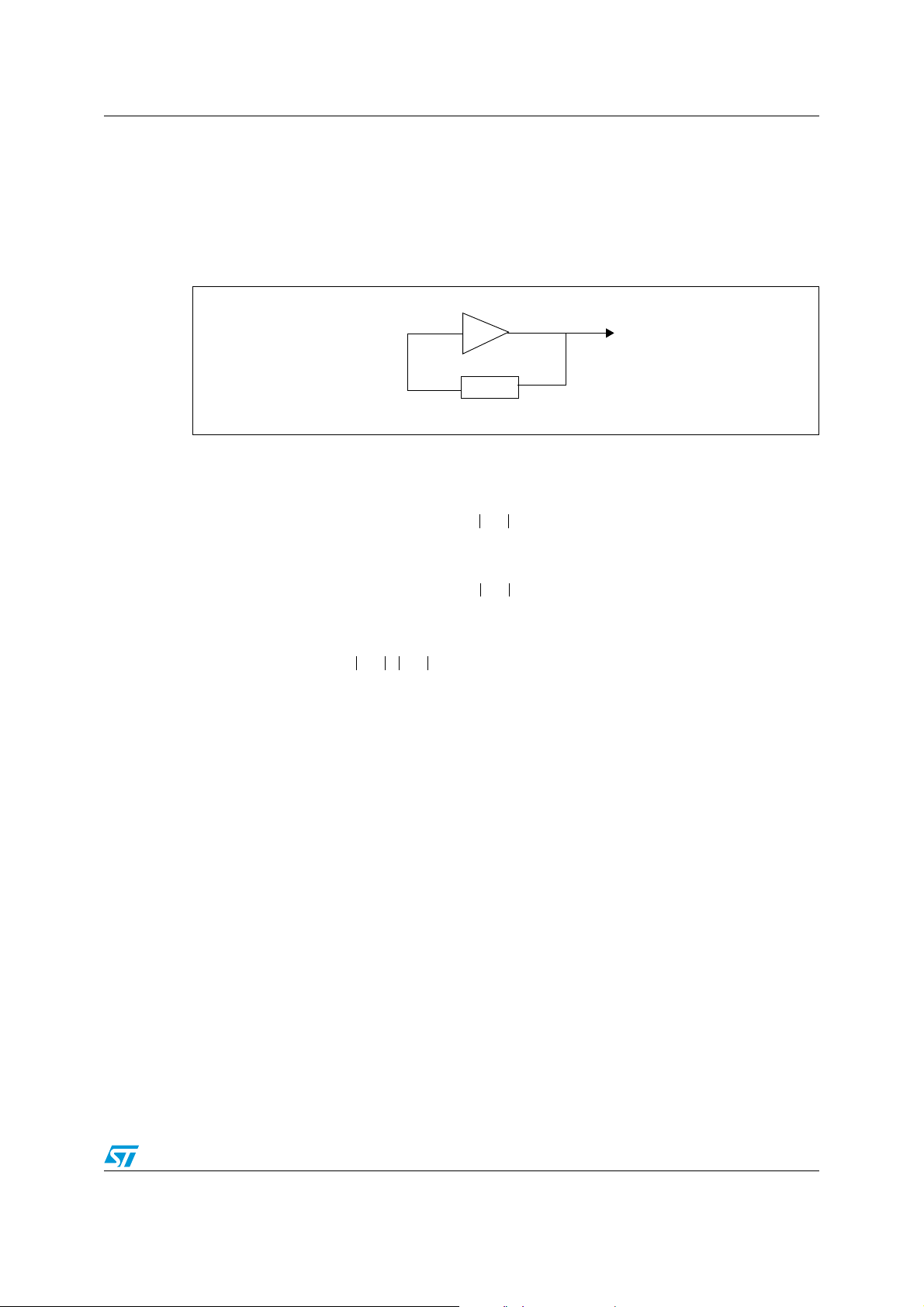
1 Oscillator theory
An oscillator consists of an amplifier and a feedback network to provide frequency selection.
The following figure shows the block diagram of the basic principle.
Figure 1. Oscillator principle
Active element
A(f)
Vout
B(f)
Passive feedback element
Where:
A(f) is the complex transfer function of the amplifier providing energy to the loop in
order to keep it oscillating.
Af() Af() e
⋅=
jfα f()
B(f) is the complex transfer function of the feedback which is setting the oscillator
frequency.
Bf() Bf() e
⋅=
jfβ f()
To oscillate, the following Barkhausen conditions must be fulfilled. The closed loop gain
should be greater than 1 and the total phase shift of 360° is to be provided.
Af() Bf() 1≥⋅
and
α f() βf()+ 2π=
In order to get the oscillator to start up, it needs initial electrical energy. Power-up transients
as well as noise can supply the needed energy. However, the energy level should be high
enough to trigger oscillation at the required frequency. Mathematically, this is represented by
|A(w)|.|B(w)| >> 1 which means that the open loop gain should be much higher than 1. The
time until steady oscillations are reached depends on the open loop gain.
3/14
Page 4
Quartz crystal characteristics AN2441
2 Quartz crystal characteristics
A quartz crystal is a piezoelectric device transforming electrical energy to mechanical
energy and vice versa. The transformation occurs at the resonant frequency. It can be
modeled as follows:
Figure 2. Quartz equivalent circuitry
R
Where:
C
represents the shunt capacitance resulting from the capacitor formed by the
0
electrodes and the parasites of the contacts.
L (motional inductance) represents the vibrating mass of the crystal.
C (motional capacitance) represents the elasticity of the crystal
R represents the circuit losses.
LC
C
0
Because R is normally negligible, the impedance of this circuitry is given by the following
equation:
2
j
--- -
Z
---------------------------------------------------
×=
w
w
C
C+()w2LCC
0
LC 1–
–
0
The following figure represents the quartz reactance across its operating frequency:
Figure 3. Quartz crystal reactance across frequency
Impedance
Area of usual parallel
resonance
reactive
0
capacitive
Series Resonance
F
s
Anti Resonance
F
a
Frequency
4/14
Page 5
AN2441 Quartz crystal characteristics
Two resonant frequencies can be calculated.
● The series-resonance frequency F
is attained when the impedance Z approaches 0.
s
F
s
1
-------------------=
2π LC
The phase shift at the series resonance frequency is zero. At the series resonance, the
impedance is minimal and the current flow is maximal.
● The anti resonance frequency F
is attained when the impedance Z approaches the
a
infinity.”
FaFs1
C
------ -+=
C
0
The area between F
and Fa is called the “usual parallel resonance” or simply “parallel
s
resonance”
When the crystal operates in parallel resonance, its frequency F
has the following expression
Parallel resonance means that a small capacitance called load capacitance C
placed across the crystal terminals to obtain the desired operating frequency.
Figure 4 shows load capacitance with the crystal equivalent circuitry.
Figure 4. Load capacitance across a parallel resonant quartz
R
2.1 Frequency vs. mode
FpFs1
LC
C
0
C
L
--------------------+=
CLC+
is between Fs and Fa and
p
C
0
should be
L
A crystal resonance can occur:
● at the F
or Fp frequencies (formulas given earlier). This is the fundamental mode
a
which is used for frequencies smaller than 30 MHz.
● at an odd multiple of the F
or Fp (harmonics of Fa or Fp). These are the third, fifth, (...)
a
overtone frequencies. This mode is used for frequencies above 30 MHz.
The crystal must be specified to operate at the desired frequency and on the desired
overtone. One should never attempt to order a crystal operating at its fundamental
frequency and operate it at an overtone frequency.
5/14
Page 6

Quartz crystal characteristics AN2441
2.2 Direct drive
Quartz drive level is the power dissipated through the crystal while operating. It is usually
expressed in terms of mW. Crystal units are specified to have a maximum drive level which
changes with frequency and operating mode.
It is given by the following formula:
DriveLevel RIr
where
Ir the current trough the crystal
R is the maximum resistance value of the specified crystal.
The temperature has an impact on the crystal’s frequency. The oscillator design should be
tested in the application temperature range required.
2
=
6/14
Page 7

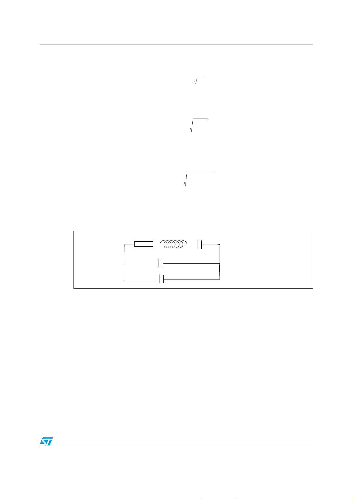
AN2441 Pierce oscillator design
3 Pierce oscillator design
Pierce oscillators are commonly used in applications because of their low consumption, low
cost and their stability. They are based on the principle in the Figure 5.
Figure 5. Pierce oscillator circuitry
RF
R
s
Quartz
C
1
C
2
3.1 Amplifier element: 74V1GU04 ST inverter + feedback resistor
The amplifier is the active element in the oscillator design.
Basically, an inverter operating with a VDD power supply has the following response:
Figure 6. An Inverter Response
V
out
V
DD
VDD/2
V
in
V
DD
The transfer function of an inverter is non-linear. However, it acts as an amplifier only in the
shaded area.
By biasing and operating the inverter near the maximum gain point, amplification is
achieved. For this reason, a resistor is connected between the input and the output of the
inverter.
V
out
V
in
For CMOS technology, typical values are between 1 MΩ and 10 MΩ. However, for TTL
technology, typical values are around several hundred Ω.
In our example, the STMicroelectronics unbuffered inverter 74V1GU04 and a 2MΩ feedback
resistor have been selected for the oscillator design.
The inverter creates 180° phase shift. In order to satisfy the Barkhausen’s criteria phase
condition for oscillation, a suitable feedback element should create the additional 180°
phase delay. This is ensured by using a crystal operating at parallel resonance.
7/14
Page 8

Pierce oscillator design AN2441
Once the crystal is selected according to the frequency and temperature range
requirements of the application, a selection is necessary of the remaining components for
the oscillator: C
, C2 and Rs. The section below assists in this process.
1
3.2 C1 and C2 capacitor selection
A parallel resonant crystal manufacturer specifies the load capacitance needed. This value
is the load seen by the crystal which is in series with C
Load capacitance should be selected, at least to start with, per the data specified in the
crystal datasheet. C
has the following formula
L
C1C2×
-------------------- C
C
L
C
1C2
+=
+
where:
is the pin capacitance and board or trace PCB-related capacitance. Typically, it is
C
stray
between 2pF and 7pF. Please refer to the PCB hints in order to minimize its value.
and C2, including all parasites.
1
stray
In order to have a phase shift of 180°, C
As an example:
Assuming that C
C
= C2 = 20pF. The normalized value of 22pF is used.
1
Using 22pF as the C
= 5pF and that the crystal load capacitance is 15pF:
stray
capacitance instead of 20pF slightly changes the parallel resonance
L
frequency. However larger changes alter the resulting frequency. For frequency accuracy,
the designer should select C
1
capacitance specified by the manufacturer.
The oscillator start-up time depends on the crystal characteristics as well as C
values.
If C
and C2 increase, the start-up time increases. Therefore, C1 and C2 should be kept
1
small but robust enough to provide adequate gain for start-up.
If the oscillator’s start up time needs to be improved because of the application
requirements, C
is increased compared to C1. This causes greater phase shift across the
2
crystal at power-up, which can speed the oscillator start up.
3.3 Rs resistor selection
Rs resistor is used in order to limit the output of the inverter so that the crystal is not over
driven. The minimum value recommended depends on the crystal characteristics. Note that
over-driving of the crystal can be observed on the oscillator output signal (where the signal
is non-symmetrical or is oscillating at the harmonic frequency). Crystal over-driving shortens
its life and in some cases, permanently damages it.
and C2 may have the same value.
1
and C2 values to stay as close as possible to the load
and C2
1
Ideally the inverter provides 180° phase shift, but the inherent delay of the inverter provides
additional phase shift. In order to ensure the total 360° shift delay, R
decrease the shift delay in the feedback loop.
R
and C2 form a voltage dividing circuit. Acceptable results can be reached by choosing the
s
value of R
8/14
equal to the C2 capacitive reactance.
s
can be used to
s
Page 9

AN2441 Pierce oscillator design
The recommended way to optimize Rs is to first choose C1 and C2 values as explained
earlier and connect a potentiometer in place of R
approximately equal to C
capacitive reactance, and then adjusted if required until an
2
. Its initial setting should be set to be
s
acceptable output and crystal drive level are found. The output signal should also be in line
with the minimum and maximum V
and VIH voltages applied on the STR71x CK pin.
IL
To have a square signal, a schmidt trigger device can be added at the inverter’s output.
Figure 7. Square wave oscillator
Square output signal
The STR71x device embeds an on-chip schmidt trigger on the CK pin so is not needed in
this example, thus making the solution more cost-effective.
The designed oscillator is mounted on an STR7 generic board. The STR71x PLL is
configured to generate 48 MHz from the 16-MHz oscillator output and a GPIO pin level is
toggled before and after PLL lock. This test is passed successfully.
For design robustness, the signal obtained should be tested in a worst case scenario:
● Application at highest temperature and lowest V
● Application at minimum temperature and highest V
voltage.
DD
DD
voltage.
9/14
Page 10

16-MHz oscillator example AN2441
4 16-MHz oscillator example
In this section, the steps and guidelines described in the previous section are put into
practice in order to design a 16-MHz oscillator.
The first step concerns the discrete components selection:
● The STMicroelectronics non-buffered inverter 741VGU04STR operating with VDD =
3.3 is selected for this application. In order to make the inverter act as an amplifier, a
2MΩ resistor is put between its input and output pads (Rf = 2M)
● The 16-Mhz quartz CQ is selected. C1 and C2 are selected according to the Quartz
specification. According to the quartz characteristics, a loading capacitor of 20pF
makes the quartz operate at its16 MHz parallel frequency. Theoretically, if we consider
an 8pF stray capacitance, C1 and C2 are calculated using the formula on Section 3.2
on page 8.
C1 = C2 = 24pF.
The standard value of 22pF is taken for both C1 and C2.
After soldering these components without the Rs resistor, the oscillator output signal is
captured in the following figure.
The signal obtained is not symmetric. Therefore, an Rs resistor is put between the inverter
output and the quartz. To start, a potentiometer is put between these two nodes and with a
variable Rs resistor, the following signal is obtained for Rs = 1 KΩ.
10/14
Page 11

AN2441 16-MHz oscillator example
The following figure gives the start-up time of the designed oscillator (~580µs).
With Ch2 as VDD and Ch1 as the output signal.
The complete schematic of the implemented oscillator is given by the following figure.
In the next section, a number of PCB hints are given to reduce the noise that can affect the
oscillator
11/14
Page 12

PCB hints AN2441
5 PCB hints
This section gives some design guidelines that must be respected for good oscillator design.
● A large stray capacitance and large inductances must be kept to a minimum to avoid an
undesired mode of oscillation, and problems with startup. In addition, high frequency
signals should be avoided near the oscillator circuitry.
● Trace lengths should be kept as short as possible. Ground plans should be used to
isolate signals and reduce noise.
● Use decoupling capacitors between each V
and its nearest VSS to smooth noise.
DD
12/14
Page 13

AN2441 Revision history
6 Revision history
Table 1. Document revision history
Date Revision Changes
02-Apr-2007 1 Initial release.
13/14
Page 14

AN2441
Please Read Carefully:
Information in this document is provided solely in connection with ST products. STMicroelectronics NV and its subsidiaries (“ST”) reserve the
right to make changes, corrections, modifications or improvements, to this document, and the products and services described herein at any
time, without notice.
All ST products are sold pursuant to ST’s terms and conditions of sale.
Purchasers are solely responsible for the choice, selection and use of the ST products and services described herein, and ST assumes no
liability whatsoever relating to the choice, selection or use of the ST products and services described herein.
No license, express or implied, by estoppel or otherwise, to any intellectual property rights is granted under this document. If any part of this
document refers to any third party products or services it shall not be deemed a license grant by ST for the use of such third party products
or services, or any intellectual property contained therein or considered as a warranty covering the use in any manner whatsoever of such
third party products or services or any intellectual property contained therein.
UNLESS OTHERWISE SET FORTH IN ST’S TERMS AND CONDITIONS OF SALE ST DISCLAIMS ANY EXPRESS OR IMPLIED
WARRANTY WITH RESPECT TO THE USE AND/OR SALE OF ST PRODUCTS INCLUDING WITHOUT LIMITATION IMPLIED
WARRANTIES OF MERCHANTABILITY, FITNESS FOR A PARTICULAR PURPOSE (AND THEIR EQUIVALENTS UNDER THE LAWS
OF ANY JURISDICTION), OR INFRINGEMENT OF ANY PATENT, COPYRIGHT OR OTHER INTELLECTUAL PROPERTY RIGHT.
UNLESS EXPRESSLY APPROVED IN WRITING BY AN AUTHORIZED ST REPRESENTATIVE, ST PRODUCTS ARE NOT
RECOMMENDED, AUTHORIZED OR WARRANTED FOR USE IN MILITARY, AIR CRAFT, SPACE, LIFE SAVING, OR LIFE SUSTAINING
APPLICATIONS, NOR IN PRODUCTS OR SYSTEMS WHERE FAILURE OR MALFUNCTION MAY RESULT IN PERSONAL INJURY,
DEATH, OR SEVERE PROPERTY OR ENVIRONMENTAL DAMAGE. ST PRODUCTS WHICH ARE NOT SPECIFIED AS "AUTOMOTIVE
GRADE" MAY ONLY BE USED IN AUTOMOTIVE APPLICATIONS AT USER’S OWN RISK.
Resale of ST products with provisions different from the statements and/or technical features set forth in this document shall immediately void
any warranty granted by ST for the ST product or service described herein and shall not create or extend in any manner whatsoever, any
liability of ST.
ST and the ST logo are trademarks or registered trademarks of ST in various countries.
Information in this document supersedes and replaces all information previously supplied.
The ST logo is a registered trademark of STMicroelectronics. All other names are the property of their respective owners.
© 2007 STMicroelectronics - All rights reserved
STMicroelectronics group of companies
Australia - Belgium - Brazil - Canada - China - Czech Republic - Finland - France - Germany - Hong Kong - India - Israel - Italy - Japan -
Malaysia - Malta - Morocco - Singapore - Spain - Sweden - Switzerland - United Kingdom - United States of America
www.st.com
14/14
 Loading...