

Page 1

AN2439
Application note
27 W Output power ultra wide range input
flyback converter
Introduction
As the telecommunications market grows, the need for suitable PSUs (Power Supply Unit)
for equipment grows as well. For products used in telecommunications, the available
voltage is either the mains voltage (from 88 V
V
). Power supplies that are able to manage input AC voltage in the full range of 88Vrms
DC
to 265Vrms are quite common while ultra wide range (from 36 V
supplies are not as common. The main advantage in using a UWR PSU is the savings in
design and qualification. Instead of designing and qualifying two PSUs, the work is done
once. Cost advantages come from bigger volume production as there is just one product
that meets a larger range of electrical specifications.
Disadvantages are the difficulties in having a high performance system in working
condition. This application note describes a UWR flayback converter that can be used to
supply a DSLM (DSL Multiplexer).
The advantage in using a flyback converter in this application is the moderate variation of
the duty cycle with the input voltage. The main drawback is the high value of the rms current
in the secondary winding, in the output diode and in the output capacitor.
to 265 VAC) or 48 VDC (from 36 VDC to 72
AC
to 264 VAC) power
DC
June 2007 Rev 1 1/20
www.st.com
Page 2

Contents AN2439
Contents
1 Board description . . . . . . . . . . . . . . . . . . . . . . . . . . . . . . . . . . . . . . . . . . . 3
1.1 Active start-up with external high voltage current source [2.] . . . . . . . . . . . 4
1.2 Slope compensation . . . . . . . . . . . . . . . . . . . . . . . . . . . . . . . . . . . . . . . . . . 5
1.3 Input section . . . . . . . . . . . . . . . . . . . . . . . . . . . . . . . . . . . . . . . . . . . . . . . . 7
1.4 Buck DC-DC converter post regulator [3.] . . . . . . . . . . . . . . . . . . . . . . . . . 7
1.5 Flyback converter . . . . . . . . . . . . . . . . . . . . . . . . . . . . . . . . . . . . . . . . . . . . 8
1.6 Transformer . . . . . . . . . . . . . . . . . . . . . . . . . . . . . . . . . . . . . . . . . . . . . . . 13
1.7 Board tests . . . . . . . . . . . . . . . . . . . . . . . . . . . . . . . . . . . . . . . . . . . . . . . . 13
1.8 Start-up tests . . . . . . . . . . . . . . . . . . . . . . . . . . . . . . . . . . . . . . . . . . . . . . 13
1.9 Dynamic load regulation tests . . . . . . . . . . . . . . . . . . . . . . . . . . . . . . . . . 14
1.10 Steady state tests . . . . . . . . . . . . . . . . . . . . . . . . . . . . . . . . . . . . . . . . . . . 16
1.11 Static load and line regulation . . . . . . . . . . . . . . . . . . . . . . . . . . . . . . . . . 16
2 Conclusions . . . . . . . . . . . . . . . . . . . . . . . . . . . . . . . . . . . . . . . . . . . . . . . 19
3 References . . . . . . . . . . . . . . . . . . . . . . . . . . . . . . . . . . . . . . . . . . . . . . . . 19
4 Revision history . . . . . . . . . . . . . . . . . . . . . . . . . . . . . . . . . . . . . . . . . . . 19
2/20
Page 3

AN2439 Board description
1 Board description
The electrical specifications for this converter are listed in the table below:
Table 1. Electrical specifications
Item Value
Isolated Yes
Input AC and DC voltage
Minimum DC input voltage 36 V
Maximum DC input voltage 72 V
Minimum AC input voltage 88 V
Maximum AC input voltage 265 V
Number of outputs 2
Output voltage 1 5 V
Output voltage 2 3.3 V
Maximum output current 1 2 A
Maximum output current 1 5 A
Maximum precision error on output 1 3%
Maximum precision error on output 2 3%
Total output power 27 W
As already specified, the selected topology is a flyback converter. In continuous mode the
relation between output and input voltage of the converter is:
Equation 1
nV
V
OUT
-------------- n
V
IN
Where n is the turn ratio and V
D
-------------
• D
1D–
the reflected voltage. It is easy to verify that for an input
R
voltage that changes between 36 V and 375 V and 70 V as reflected
•
nV
IN
(
375V 2 265•=
OUT
•+
OUT
--------------------------------------- -
V
V
---------------------- -==⇒=
VINVR+
)V
R
voltage, the duty cycle changes from about 70% (at minimum input voltage) to about 16%.
Buck type topologies are not suitable because the duty cycle varies widely (from 9%- to 90%
for a forward converter in the same condition for example), worsening the efficiency and
making the design very complex.
A second design choice was to use a switching post regulator that has, as input voltage, the
output voltage of the flyback and the output as 3.3 V. The purpose of this is to meet the
requested precision in both outputs and to avoid using another secondary winding where
the root mean square current would be very high. Assuming a 90% of efficiency for this step
down converter, the total current sunk from the output of the flyback is 5.7 A. The buck
converter for the post regulation is described in Section 1.4 on page 7.
In order to limit the high root mean square current at the secondary side, another design
choice was to have a flyback converter that works, most of the time, in continuous
conduction mode. The controller used in this application is the L5991 [1.] which is a current
3/20
Page 4
Board description AN2439
mode controller. In continuous conduction mode for the lower input voltages, the duty cycle
is greater than 50% which requires a slope compensation to ensure stable operation of the
current loop. The slope compensation is implemented through a circuit described in
Section 1.2 on page 5.
The switching frequency was selected to be equal to 70 kHz and the reflected voltage to be
equal to 70 V.
In order to have the same wake-up time for the different input voltages, an active start-up
was implemented instead of the most commonly used passive circuits. The active start-up
circuit is described in Section 1.1.
In order to improve efficiency, the converter has two different inputs, one for the AC voltage
(88 V
ACrms
to 265 V
) and one for the DC voltage (36 VDC to 72 VDC). The input stage
ACrms
of the converter is described in Section 1.3 on page 7.
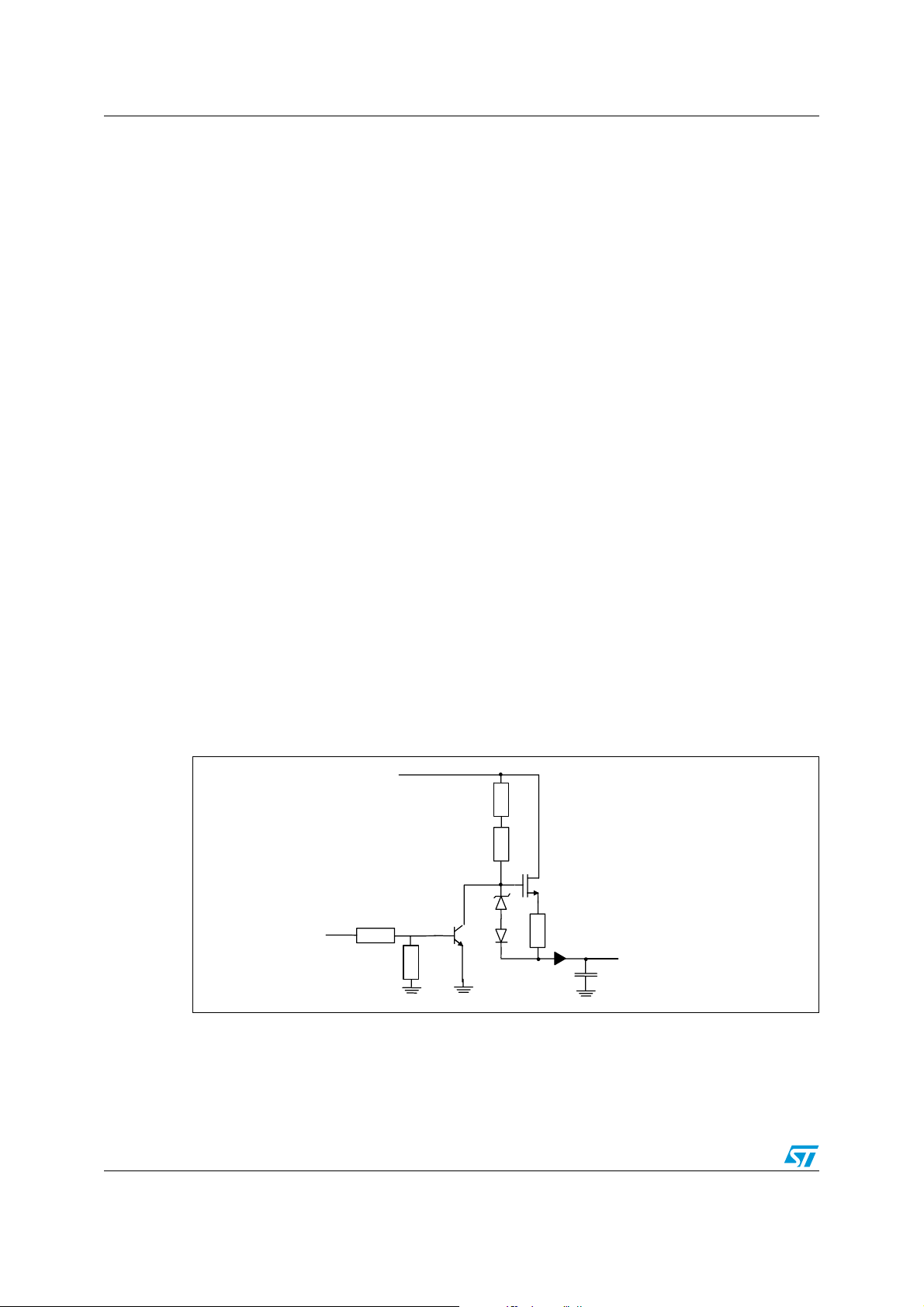
1.1 Active start-up with external high voltage current source [2.]
The circuit of the active start-up is shown in Figure 1. Through R1 and R2 the 600 V
MOSFET M
diode and D
the resistor R
current provided to the capacitor connected to V
constant current generator and its current can be calculated according to the following
equation:
(STQ1NK60ZR) is switched on. The back-to-back diodes (D1 is a 15 V zener
1
is a standard diode 1N4148) are used to set the voltage between the gate and
2
pin not connected with the source of M1. The resistor R3 is used to limit the
3
of the L5991. The circuit behaves as a
CC
Equation 2
V
– VTH–
ZVd
I
------------------------------------=
R
3
Where V
biased and V
is the D1 zener break-down voltage, Vd the diode D2 voltage drop when forward
Z
is the gate to source on threshold voltage of the MOSFET M1.
TH
Figure 1. Active start up circuit
To Bulk Capacitor +
R
1
R
2
M
1
D
To V
REF
Pin of the L5991
T1
1
R
D
2
3
To V
Pin of the
CC
L5991
I
When we connect the converter to the mains, the controller (L5991) is initially off, and the
small signal bipolar transistor T
R
and R2 and the current generator starts to work charging the VCC capacitor. As the VCC
1
voltage exceeds its On Threshold, the L5991 starts to operate and sets the V
to 5 V. This voltage turns on the small bipolar transistor T
is also off. The gate of the MOSFET M1 is biased through
1
pin (pin 4)
that pulls down the gate of M1
1
REF
4/20
Page 5
AN2439 Board description
⎝⎠
switching it off. As a result, as the controller is on, the current generator stops working, and
the controller is supplied by the auxiliary winding of the flyback converter.
1.2 Slope compensation
The circuit for slope compensation is shown in Figure 2. When the main MOSFET
(STP10NK70Z) is switched on, the GD pin (Gate Driver) of the L5991 goes high up to a
voltage of about 14 V. Capacitor C
large enough, compared to the switching period, we can assume that the voltage across
capacitor C
the partition divider R
the MOSFET M
diode D
is a linear ramp. This voltage is added to the CS pin (Current Sense) through
2
. Capacitor C2 is then fast discharged and ready for the next cycle.
1
1
, R1+R
3
is switched off, the gate driver pin of the L5991 pulls down the anode of
Figure 2. Slope compensation circuit
is charged through resistor R2. If the time constant RC is
2
and provides the needed slope compensation. When
SENSE
STP10NK70
M1
RSENSE
. In this
2
CS Pin of L5991
R2 22k
C2
1.8 nF
R3
15k
Bat49
RGATEGD Pin of L5991
D1
R1 1.5k
C1
100 pF
Equation 3 gives the waveform expression of the voltage across the capacitor C
formula V
is the forward voltage drop on diode D1 and VGD is the voltage on gate driver pin
D
of the L5991 (Pin 10), when it is high. As a rule of thumb, in order to have approximately a
linear ramp across C
, the time constant C2RT is selected in the range of ten times the
2
switching period.
Equation 3
Neglecting R
VCt() V
SENSE
GD
it can be simplified as:
R1R3R
++
------------------------------------------------------------- -
R
+++
1R2R3RSENSE
SENSE
t–
--------------------
⎛⎞
C
•
2RT
1e
–
⎜⎟
+•• e
V
D
•=
t–
--------------------
C
•
2RT
Equation 4
R1R3+
t() V
V
C
R
is the equivalent resistance across capacitor C2:
T
--------------------------------- -
GD
R
++
1R2R3
Equation 5
R2R1R3– R
----------------------------------------------------------------- -
R
τ
R
+++
1R2R3RSENSE
–()•
⎛⎞
⎜⎟
⎝⎠
SENSE
C
1e
–
•
2RT
≅=
VD+•• e
R
2R1R3
--------------------------------------
R
++
1R2R3
–()•
t–
--------------------
•≅
t–
--------------------
•
C
2RT
5/20
Page 6
Board description AN2439
The slope compensation voltage added on CS Pin of the L5991 is:
Equation 6
Vst()
R
1RSENSE
------------------------------------------------
R
++
2R3RSENSE
VCt()•
R
1
--------------------
R2R3+
VCt()•≅=
–
We know that if we add a ramp whose slope is one half of the primary side equivalent
demagnetizing current slope (m
), the current loop is stable for any duty cycle lower than
a
one. As consequence the requested amount of slope compensation needed to guarantee
stable operation is:
Equation 7
V
1
R
-------
-- -
•=
S
• R
L
2
SENSE
m
m
In the last equation V
primary side. The value of R
compensation we add and of course the maximum peak current at the primary side (I
is the reflected voltage and Lm the magnetizing inductance at
R
has to be calculated taking into account the slope
SENSE
PKP
Equation 8
R
SENSE
--------------------------------------------------------- -=
I
PKP
1V
V
-------
L
D
R
MAX
-------------- -
••+
f
m
sw
1
-- -
2
The maximum value of the voltage we add at the current sense pin is:
Equation 9
V
SMAX
D
MAX
-------------- -
m
•
s
f
sw
R
1
--------------------
R2R3+
D
⎛⎞
-------------- -
V
•==
C
⎝⎠
MAX
f
sw
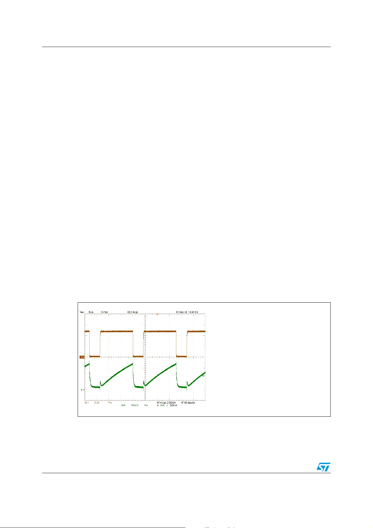
Figure 3 shows the gate driver signal and the slope compensation signal measured at the
CS pin.
Figure 3. Slope compensation signal
).
6/20
Ch1 (yellow): gate driver signal
Ch4 (green): slope compensation ramp on
current sense pin
Page 7

AN2439 Board description
V
V
1.3 Input section
The schematic of the input section is given in Figure 4. We used two separated connectors
for the AC input voltage (88 V
The system works correctly if we feed the converter with the Dc voltage in the AC input
voltage connector. We used a separated connector in order to gain efficiency.
Using the additional connector for the Dc input voltage we use two different NTCs to limit the
inrush current in the two cases. NTC1 has to limit the inrush current, considering as worst
case the maximum AC Peak input voltage. NTC2 has to limit the inrush current, considering
as worst case the maximum DC voltage (72 V) which means that NTC2 can be lower than
NTC1 and dissipates less energy.
The DC voltage is connected to the bulk capacitors through one diode (used for protection in
case we connect the Dc input with the wrong polarity) so we cut one half of power
dissipation compared to the power we would dissipate in the bridge.
Figure 4. Input section
t
1 2
NTC18. 2 2A
Ac Input
oltage
J1
2
1
CON2
1 2
+
Dc Input
oltage
J2
CON2
-
2
1
to 265 VAC) and for the DC input voltage (36 VDC to 72VDC).
AC
Start up C ir c uit
C1
1nF Y1
C2
100nF
C3
1nF Y1
2
-+
BR1
BRIDGE
3
1
4
F1 2A
C5
33 uF
4
3
FILTER1
Lin Filt er
1
2
t
NTC2.82 2A
D8 600V 3A diode
C222
100nF
Primary +
C4
33uF
1.4 Buck DC-DC converter post regulator [3.]
The second output of 3.3 V, able to provide up to 5 A to its load, is obtained using a
switching post regulation. The post regulator is a synchronous buck converter based on the
L6725 controller and the schematic is given in Figure 5.
7/20
Page 8

Board description AN2439
+
Figure 5. Synchronous buck converter post regulator
C31
100nF
R24 0.1
C21
1uF Ceramic Cap
R25 6.8k
C28 220nF
C22 3.9nF R27 6.8k
C25 330pF R29
1
COMP
2
SS/INH
3
EAREF
4
OCL
5
OCH
6
PHASE
7
HGATE
8 9
BOOT PGND
U4 L6725
FB
SGND
N.C.2
N.C.1
VCC
VCCDR
LGATE
D11 STPS1L30M
16
15
14
13
12
11
10
1.5k
RG1 3.3
RG2 3.3
C23 10nFR28 330
U6
1
S1
2
S2
3
S3
4
Gate
STS9NF3LL
U5
1
8
S1
D4
2
7
S2
D3
3
6
S3
D2
4
5
Gate
D1
STS9NF3LL
8
D4
7
6
5
D12
STPS1L30M
D3
D2
D1
R26
C24
1.2k
1nF
R30
2.4k
L4 3.9uF
C26
NM
R31
NM
In+
Out-In-
Out
C27
220uF 6.3V
C30
220uF 6.3V
The two MOSFET STS12NF3LL (U5 and U6 in the schematic) are driven with 180 degrees
of phase shift. The gate driver signal value is 5 V when high, as the L6725 is supplied with
the 5 V that is, the output of the flyback main converter.
This situation is not optimum for the two MOSFETs, as their R
is higher when the gate
DSON
signal is 5 V compared to when the gate signal is 10 V [4.]. It could seem that the two
MOSFETs are oversized, but taking into account the low driving signal, they are not.
1.5 Flyback converter
The primary side of the flyback converter schematic is given in Figure 6 and the secondary
side is given in Figure 7.
The bill of material of the entire circuit is given in Ta ble 2, 3, 4, and 5.
8/20
Page 9

AN2439 Board description
A
3
A
Figure 6. Flyback converter primary side schematic
R8
22k
Primary +
Primary -
R12
15k
D5
BAT49
R11 1.5k
C8
100pF
C10
1.8nF
RCLAMPB1
18k 2W
R7 10
RSB1
0.66 1/2W
CCLAMP1
1.2nF 400V
D2
STTH1L06
STP10NK70
1
RSB2
0.66 1/2W
23
M1
23
uxiliary +
R1 1 Meg
STQ1NK60ZR
Q1
1
R5
4.7k
1 2
10uF 35V
D3
1N4148
D4
12V
D12B1STTH102
C12
R2
1 Meg
Q2
BC337
R14 10k
Start up C i rc uit
Q3 STX715
1 2
R10 100kR9 100k
D6
15Vz
R3 6. 8k 1%
5.6k 1%
CVCC1
47uF 25V
HeatSink 15 C / W
1
1
Mosfet M1 Heat Sink
R4 N.M.
RA 1
4.3k 1%
R6
C7
100nF
4.7nF
Opto Colle c t or
CSS1
C9
47nF
C11
2.2nF
1
SYNC
2
RCT
3
DC-C
4
Vref
5
VFB
6
Comp
7
SS
8
Vcc
R13 8.2
L5991
ST-BY
DC lim
SGND
PGND
16
15
14
DIS
13
CS
12
11
10
GD
9
Vc
Figure 7. Flyback converter secondary side schematic
D10
12
OPTO1
PC817
3
2 1
C13
1800uF 16V MCZ
R21
1k N. M.
R22 22k
C15
1800uF 16V MCZ
R18 470
R23
82k 1%
C17
1800uF 16V MCZ
R20
82k 1%
C191uF
Primary +
Primary -
uxiliary +
HS1
Diode D7 Heat Si nk
1
P
HeatSink 10 C/W
C212 CY1
1
3
6
7
Transf ormer
T1
14
13
9
8
Opto Collector
TEST POINT
TP2
D7 DIODE
4
3
TL1431
1
L3 8.2uH 2.5A
C14
+
1800uF 16V MCZ
Dc-Dc Coverter
In+
In-
Out+
Out-
33uF
C16
J3
1
2
3
CON
9/20
Page 10

Board description AN2439
Table 2. Input section (schematic Figure 4)
Quantity Part reference Part name Description
1 BR1 Bridge 600 V 3 A Bridge diodes
2 C3,C1 1 nF Y1
1 C2, C222 100 nF
1NTC2.82 2ª
1 D8 600 V 3 A 600 V 3 A diode
1F12 A
2 C4, C5 33 µF 400 V Electrolytic capacitor
1 Filter1 4.7 mH 3A Line filter
1 NTC1 8.2 2ª
Table 3. Primary side flyback converter (schematic Figure 6)
Quantity Part reference Part name Description
2R2,R11 Meg
1 R5 4.7 k
2 R10,R9 100 k
1 R3 6.8 k 1%
1 R6 5.6 k 1%
1 R14 10 k
1 RA1 4.3 k 1%
1R4N.M.
1 R13 8.2
1 R12 15 k
1 R8 22 k
1R710
1 R11 1.5 k
2 RSB2,RSB1 0.66 1/2 W
1 RCLAMPB1 18 k 2 W
1 U2 L5991
1D2STTH1L06
STMicroelectronics primary controller
with standby
STMicroelectronics turbo 2 ultra fast high
voltage rectifier
1 D3 1N4148
1 D4 12Vz 12 V Break down Zener diodeo
1D5BAT42
10/20
STMicroelectronics small signal Schottky
diode
Page 11

AN2439 Board description
Table 3. Primary side flyback converter (schematic Figure 6) (continued)
Quantity Part reference Part name Description
1D615Vz
1 Q1 STQ1NK60ZR
1Q2BC337
1 Q3 STX715 STMicroelectronics NPN transistor
1 U1 HeatSink 15 C/W
1M1STP10NK70Z
1 D12B1 STTH102
1 C12 10 µF 35 V
1 CVCC1 47 µF 25 V
1 CCLAMP1 1.2 nF 400 V
1 CSS1 47 nF
1 C8 100 pF
1 C9 4.7 nF
1 C10 1.8 nF
1 C11 2.2 nF
4 C2 100 nF
STMicroelectronics N-CHANNEL 600 V
SuperMESH™ MOSFET
STMicroelectronics N-Channel 700 V
Zener-protected SuperMESH™
MOSFET
STMicroelectronics high efficiency ultra
fast diode
Table 4. Secondary side flyback (schematic Figure 7)
Quantity Part reference
1C212CY1
1 C16 33 µF
4
1C191µF
1 D7 STPS16H100
1 T1 Transformer
1 D10 TL1431
1C241nF
1R18470
2 R20,R23 82 k 1%
C13, C14, C15,
C17
Part name or
value
1800 µF 16 V
MCZ
Rubycon high current low ESR
electrolytic capacitor
STMicroelectronics high voltage power
Schottky rectifier
STMicroelectronics programmable
voltage reference
Description
11/20
Page 12

Board description AN2439
Table 4. Secondary side flyback (schematic Figure 7) (continued)
Quantity Part reference
1R211k N.M.
1 L3 8.2uH 2.5°
2 R22,R8 22k
1 OPTO1 PC817 Optocoupler
Part name or
value
Table 5. DC-DC converter (schematic Figure 4)
Quantity Part reference
1 C25 330 pF
1 R24 0.1 Ω
2 R25,R27 6.8 kΩ
1 R26 1.2 kΩ
1 R28 330 Ω
1 R29 1.5 kΩ
1 R30 2.4 kΩ
1R31N.M.
2 RG2,RG1 3.3 Ω
1 C21 1 µF Ceramic capacitor
Part name or
value
Description
Description
1 C22 3.9 nF
1 C23 10 nF
1 C24 1 nF
1 C25 330 pF
1 C26 N.M. Not mounted
1 C27, C30 220 µF 6.3 V ZA Rubycon ZA electrolytic capacitor
1 C28 220 nF
4 C31 100 nF
2 D12,D11 STPS1L30M
1 L4 3.9 µF 6A Rated current inductor
1 U4 L6725
2 U5,U6 STS12NF3LL
STMicroelectronics low drop power
Schottky rectifier
STMicroelectronics low cost adjustable
step-down controller
STMicroelectronics N-Channel 30 V low
gate charge STripFET™ II Power
MOSFET
12/20
Page 13

AN2439 Board description
1.6 Transformer
The details of the transformer used are listed below.
● Electrical characteristics
– Primary inductance value: 450
– Primary leakage inductance: 12
● Magnetic core
– Material: N67
–Type: ETD29
– Air gap: ≈ 0.2 mm
Table 6. Winding size
Winding Number of turns Wire size
Primary winding 46 AWG26
Secondary winding 4 AWG26X4
Auxiliary winding 10 AWG40
Figure 8 describes the used and suggested placing of the windings.
µH
µH
Figure 8. Transformer winding placing
Insulation
Auxiliary Winding
Secondary Winding
1.7 Board tests
The tests performed aim to evaluate the converter behavior in terms of efficiency, safe
operating area of the devices, and line and load regulation.
1.8 Start-up tests
½ Primary Winding
½ Primary Winding
In a flyback converter the most critical conditions for the mains switch (when no abnormal
event occurs), in terms of maximum drain current and of maximum drain voltage, are during
the start-up phase. The max values for drain voltage and current were measured in both full
13/20
Page 14

Board description AN2439
load and no load condition that are the two extreme points in terms of load and for minimum,
maximum, and nominal input voltages. The results are shown in Tabl e 7 .
Table 7. Start-up measures
V
in
V
drainMax
(V) I
No load Full load No load Full load
36 V
48 V
72 V
88 V
115 V
230 V
265 V
DC
DC
DC
AC-rms
AC-r ms
AC-r ms
AC-r ms
235 288 2.03 2.55
256 313 2.09 2.66
277 320 2.07 2.50
320 318 2.06 2.26
362 391 2.18 2.45
526 543 2.37 2.54
562 581 2.13 2.5
The drain voltage is well below the break down voltage of the MOSFET. In the worst case
there is at least 100 V of safety margin. The maximum peak value of the drain current,
during the start-up phase, is higher then the steady state value (around 2 A). The difference
is not too high, thanks also to the soft start, and it means that there is no risk for the
transformer to saturate during start-up.
1.9 Dynamic load regulation tests
The behavior of the system was verified also in dynamic load condition. Both loads are
square wave shaped. Both have step change between 10% and 90% of their respective
maximum nominal load and vice versa. The results are shown in Figure 9.
drainMax
(A)
14/20
Page 15

AN2439 Board description
Figure 9. Dynamic load waveforms
a
b
Ch1 (yellow): 5 V output voltage
Ch4 (green): 3.3 V output voltage
Ch2 (blue): load current of the 5 V
output
Ch2 (purple): load current of the 3.3 V
output
c
15/20
Page 16

Board description AN2439
1.10 Steady state tests
The aim of these tests is to evaluate the performance of the converter in steady state
condition, measuring the converter efficiency for minimum, maximum and nominal input
voltages.
Table 8. Steady state full load and half load condition efficiency measures
Vin (V) Full load Half load
P
36 V
48V
72V
88V
115 V
230V
265V
DC
DC
DC
AC
AC
AC
AC
(W) P
IN
43.5 27 62 19.4 13.5 70
39.8 27 68 18.7 13.5 72
37.6 27 72 18.3 13.5 74
38.6 27 70 19.2 13.5 70
37.8 27 71 18.9 13.5 71
37.4 27 72 19.1 13.5 71
37.5 27 72 19.2 13.5 70
(W) η (%) PIN (W) P
OUT
(W) η (%)
OUT
The efficiency as it is possible to see from Ta b l e 8 is not high, ranging between 64% and
72% in full load condition and between 70% and 74% in half load condition. The main
reason of this poor efficiency is the high power dissipation on the output diode of the flyback
(more than 5 W at low input voltage) that returns to the rest of the flyback converter. The
transformer has to deliver more power than necessary, increasing the losses on the
transformer itself. Because of this, the power MOSFET has to conduct more current than
necessary. The Input section is also affected because the diode or the bridge diodes and the
NTC have to conduct higher current.
Figure 10. Efficiency chart
Efficie ncy
75
70
65
60
30 80 130 180 230 280
Full Load
Half Load
1.11 Static load and line regulation
These tests aim to evaluate the precision of the output voltage and how it is affected by line
voltage and load in steady state condition. Tabl e 9 and Tab l e 1 0 show the output voltages in
different load conditions for different input voltages. For the 5 V output the minimum and
maximum values are 5.099 V and 5.145 V inside the tolerance specified in Ta bl e 1 . The
16/20
Page 17

AN2439 Board description
minimum and maximum values for the 3.3 V output are 3.348 and 3.357 which are both
inside the tolerance.
Table 9. Static line and load regulation
Vin (V) Both output in full load Both output in no load
V
36 V
48 V
72 V
88 V
115 V
230 V
265 V
DC
DC
DC
AC
AC
AC
AC
(V) V
OUT1
5.099 3.357 5.145 3.351
5.099 3.355 5.145 3.351
5.100 3.354 5.144 3.351
5.100 3.355 5.145 3.350
5.100 3.355 5.145 3.350
5.100 3.352 5.145 3.350
5.100 3.352 5.145 3.351
(V) V
OUT2
(V) V
OUT1
OUT2
(V)
Table 10. Static line regulation and crossed load regulation
Vin (V) V
36 V
DC
48 V
DC
72 V
DC
88 V
AC
115 V
AC
230 V
AC
265 V
AC
Full load V
OUT1
V
(V) V
OUT1
no load Vout1 No load Vout2 full load
OUT2
(V) V
OUT2
(V) V
OUT1
5.116 3.348 5.129 3.357
5.116 3.348 5.129 3.357
5.116 3.348 5.129 3.357
5.117 3.349 5.129 3.356
5.117 3.349 5.129 3.356
5.117 3.349 5.129 3.356
5.117 3.349 5.129 3.356
Figure 11 and Figure 12 show the drain voltage (Ch3, purple waveform) and current (Ch2
blue waveform) of the flyback MOSFET. Figure 11 shows the waveforms when the circuit is
fed with the input voltage of 36 V
shows when the input is 265 V
, which is the minimum input voltage, and Figure 12
DC
which is the maximum input voltage.
AC
The load is the maximum for both the output. Figure 11 and Figure 12 allow comparing the
difference between the two extreme points of the input voltage range. When the input is at
its minimum, the flyback is working in continuous mode with a peak current close to 2 A and
a maximum duty cycle near to 75%. When the input voltage is at its maximum, the system
works in discontinuous mode with a duty cycle close to 15% and a peak current of about 1.8
A. Figure 13 shows the same waveforms when circuit is fed with the nominal values of the
input voltage (48 V
, 115 VAC and 230 VAC) and in full load condition.
DC
OUT2
(V)
17/20
Page 18

Board description AN2439
Figure 11. Steady state waveforms with
minimum and maximum input
voltage - full load at 36 V
DC
Figure 13. Steady state waveforms with nominal input voltage
Figure 12. Steady state waveforms with
minimum and maximum input
voltage - full load at 264 V
AC
a
c
18/20
b
Ch2 (blue): drain current
Ch3 (purple): drain voltage
(a) Full load waveforms at 48 V
(b) Full load waveforms at 115 V
(c) Full load waveforms at 230 V
DC
AC
AC
Page 19

AN2439 Conclusions
2 Conclusions
In this application note an ultra-wide range input voltage converter was presented. The
topology used for the main converter is the well known flyback topology. The additional
circuits used as active start-up circuit and slope compensation were described in detail. The
tests results of the board were also presented. The most obvious result is the moderate
efficiency of the converter. This result is only slightly related to the ultra wide range input. It
is mainly due to the low output voltage and high current load of the flyback converter. In the
secondary side flyback diode, the power dissipation is close to 5 W. This high power
dissipation in the secondary side affects the performances, in terms of power dissipation, of
the transformer, the primary side part of the flyback and of the input section.
In order to increase efficiency we can use a flyback with higher output voltage, 12 V for
example, for the same power rate and obtain the output voltages requested in the electrical
specifications with two switching post regulators. In this case, of course, the cost increases.
3 References
1. L5991 datasheet
2. AN1729 "L6565 - Based low cost SMPS for TV with Less then 1 W stand by
consumption"
3. L6725 datasheet
4. STS12NF3LL datasheets
4 Revision history
Table 11. Revision history
Date Revision Changes
25-Jun-2006 1 First issue
19/20
Page 20

AN2439
Please Read Carefully:
Information in this document is provided solely in connection with ST products. STMicroelectronics NV and its subsidiaries (“ST”) reserve the
right to make changes, corrections, modifications or improvements, to this document, and the products and services described herein at any
time, without notice.
All ST products are sold pursuant to ST’s terms and conditions of sale.
Purchasers are solely responsible for the choice, selection and use of the ST products and services described herein, and ST assumes no
liability whatsoever relating to the choice, selection or use of the ST products and services described herein.
No license, express or implied, by estoppel or otherwise, to any intellectual property rights is granted under this document. If any part of this
document refers to any third party products or services it shall not be deemed a license grant by ST for the use of such third party products
or services, or any intellectual property contained therein or considered as a warranty covering the use in any manner whatsoever of such
third party products or services or any intellectual property contained therein.
UNLESS OTHERWISE SET FORTH IN ST’S TERMS AND CONDITIONS OF SALE ST DISCLAIMS ANY EXPRESS OR IMPLIED
WARRANTY WITH RESPECT TO THE USE AND/OR SALE OF ST PRODUCTS INCLUDING WITHOUT LIMITATION IMPLIED
WARRANTIES OF MERCHANTABILITY, FITNESS FOR A PARTICULAR PURPOSE (AND THEIR EQUIVALENTS UNDER THE LAWS
OF ANY JURISDICTION), OR INFRINGEMENT OF ANY PATENT, COPYRIGHT OR OTHER INTELLECTUAL PROPERTY RIGHT.
UNLESS EXPRESSLY APPROVED IN WRITING BY AN AUTHORIZED ST REPRESENTATIVE, ST PRODUCTS ARE NOT
RECOMMENDED, AUTHORIZED OR WARRANTED FOR USE IN MILITARY, AIR CRAFT, SPACE, LIFE SAVING, OR LIFE SUSTAINING
APPLICATIONS, NOR IN PRODUCTS OR SYSTEMS WHERE FAILURE OR MALFUNCTION MAY RESULT IN PERSONAL INJURY,
DEATH, OR SEVERE PROPERTY OR ENVIRONMENTAL DAMAGE. ST PRODUCTS WHICH ARE NOT SPECIFIED AS "AUTOMOTIVE
GRADE" MAY ONLY BE USED IN AUTOMOTIVE APPLICATIONS AT USER’S OWN RISK.
Resale of ST products with provisions different from the statements and/or technical features set forth in this document shall immediately void
any warranty granted by ST for the ST product or service described herein and shall not create or extend in any manner whatsoever, any
liability of ST.
ST and the ST logo are trademarks or registered trademarks of ST in various countries.
Information in this document supersedes and replaces all information previously supplied.
The ST logo is a registered trademark of STMicroelectronics. All other names are the property of their respective owners.
© 2007 STMicroelectronics - All rights reserved
STMicroelectronics group of companies
Australia - Belgium - Brazil - Canada - China - Czech Republic - Finland - France - Germany - Hong Kong - India - Israel - Italy - Japan -
Malaysia - Malta - Morocco - Singapore - Spain - Sweden - Switzerland - United Kingdom - United States of America
www.st.com
20/20
 Loading...