

Page 1
AN2435
Application note
TM sepic converter in PFC pre-regulator
Introduction
For the PFC (power factor correction) converter, sepic topology can be used when an output
voltage lower than the maximum input voltage is required. This is instead of boost topology,
which is unsuitable beacuse it must have an output voltage higher than the maximum input
voltage. Sepic topology is advantageous because it allows the use of the ripple steering
technique in order to reduce the switching frequency components of the input current
without additional costs. This application note presents the basic equation of the sepic
converter, in addition to design guidelines for a sepic PFC operating in transition mode and
using the ripple steering technique. An application example with some tests results and
waveforms is also provided in the document.
Sepic converter
March 2007 Rev 1 1/25
www.st.com
Page 2

Contents AN2435
Contents
1 Sepic topology for PFC converter . . . . . . . . . . . . . . . . . . . . . . . . . . . . . . 4
1.1 Operation of the sepic converter . . . . . . . . . . . . . . . . . . . . . . . . . . . . . . . . 4
1.2 Sepic converter as a PFC circuit operating in transition mode [1.] . . . . . . . 6
1.3 Coupled inductor sepic converter and ripple steering . . . . . . . . . . . . . . . 10
1.4 Small signal model for a TM sepic converter . . . . . . . . . . . . . . . . . . . . . . 12
2 Practical design example of a sepic converter . . . . . . . . . . . . . . . . . . 13
2.1 Design specifications . . . . . . . . . . . . . . . . . . . . . . . . . . . . . . . . . . . . . . . . 13
2.2 MOSFET (M
2.3 Diode D1 selection . . . . . . . . . . . . . . . . . . . . . . . . . . . . . . . . . . . . . . . . . . 14
2.4 Capacitor C1 selection . . . . . . . . . . . . . . . . . . . . . . . . . . . . . . . . . . . . . . . 15
2.5 Output capacitor C2 selection . . . . . . . . . . . . . . . . . . . . . . . . . . . . . . . . . 15
2.6 Transformer design . . . . . . . . . . . . . . . . . . . . . . . . . . . . . . . . . . . . . . . . . . 16
2.7 Selection of other components . . . . . . . . . . . . . . . . . . . . . . . . . . . . . . . . . 17
) selection . . . . . . . . . . . . . . . . . . . . . . . . . . . . . . . . . . . . . . 14
1
3 Conclusion . . . . . . . . . . . . . . . . . . . . . . . . . . . . . . . . . . . . . . . . . . . . . . . . 18
3.1 References . . . . . . . . . . . . . . . . . . . . . . . . . . . . . . . . . . . . . . . . . . . . . . . . 18
4 Board description and bench evaluation results . . . . . . . . . . . . . . . . . 18
4.1 Board description . . . . . . . . . . . . . . . . . . . . . . . . . . . . . . . . . . . . . . . . . . . 18
4.2 Bench results . . . . . . . . . . . . . . . . . . . . . . . . . . . . . . . . . . . . . . . . . . . . . . 21
5 Revision history . . . . . . . . . . . . . . . . . . . . . . . . . . . . . . . . . . . . . . . . . . . 24
2/25
Page 3

AN2435 List of figures
List of figures
Figure 1. Basic circuit of the sepic converter . . . . . . . . . . . . . . . . . . . . . . . . . . . . . . . . . . . . . . . . . . . . 5
Figure 2. Sepic converter when the main switch is on . . . . . . . . . . . . . . . . . . . . . . . . . . . . . . . . . . . . . 5
Figure 3. Sepic converter when the main switch is off . . . . . . . . . . . . . . . . . . . . . . . . . . . . . . . . . . . . . 6
Figure 4. Inductor L1 and inductor L2 current waveform . . . . . . . . . . . . . . . . . . . . . . . . . . . . . . . . . . . 6
Figure 5. Switching frequency variation vs θ for two different input voltages. . . . . . . . . . . . . . . . . . . . 9
Figure 6. Input current in TM for sepic PFC . . . . . . . . . . . . . . . . . . . . . . . . . . . . . . . . . . . . . . . . . . . . 10
Figure 7. Coupled inductor of a sepic converter . . . . . . . . . . . . . . . . . . . . . . . . . . . . . . . . . . . . . . . . 11
Figure 8. Model of two coupled inductors . . . . . . . . . . . . . . . . . . . . . . . . . . . . . . . . . . . . . . . . . . . . . 11
Figure 9. Equivalent current source of the sepic converter . . . . . . . . . . . . . . . . . . . . . . . . . . . . . . . . 13
Figure 10. Small signal model for the TM sepic converter . . . . . . . . . . . . . . . . . . . . . . . . . . . . . . . . . . 13
Figure 11. Output diode current averaged over the switching cycles . . . . . . . . . . . . . . . . . . . . . . . . . 17
Figure 12. Transformers with symmetrical structures . . . . . . . . . . . . . . . . . . . . . . . . . . . . . . . . . . . . . 17
Figure 13. Schematic of the sepic converter . . . . . . . . . . . . . . . . . . . . . . . . . . . . . . . . . . . . . . . . . . . . 20
Figure 14. Efficiency chart . . . . . . . . . . . . . . . . . . . . . . . . . . . . . . . . . . . . . . . . . . . . . . . . . . . . . . . . . . 21
Figure 15. Main waveform of the circuit . . . . . . . . . . . . . . . . . . . . . . . . . . . . . . . . . . . . . . . . . . . . . . . . 22
Figure 16. Current of the inductors over one line cycle: V
Figure 17. Current of the inductors over switching cycles: V
Figure 18. Current of the inductors over one line cycle: V
Figure 19. Currents of the inductors over switching cycles: V
Figure 20. Input current: 230 V
Figure 21. Input current: 230 V
input, 65 W output . . . . . . . . . . . . . . . . . . . . . . . . . . . . . . . . . . . . . . 24
ac
input, 32 W output . . . . . . . . . . . . . . . . . . . . . . . . . . . . . . . . . . . . . . 24
ac
= 230 V
in
= 230 V
in
= 230 V
in
= 230 V
in
ACRMS
ACRMS
ACRMS
ACRMS
, P
= 65 W . . . . . . . . . . 23
out
, P
= 65 W . . . . . . . . 23
out
, P
= 65 W . . . . . . . . . . 23
out
, P
= 65 W . . . . . . . 23
out
3/25
Page 4

Sepic topology for PFC converter AN2435
1 Sepic topology for PFC converter
The most widely used topology in PFC applications is boost topology. It has two main
advantages:
1. The power switch is a low sided one, unlike buck and buck-boost topology where it is an
hide side one and needs a floating driving circuit.
2. The inductor is on the input side of the converter, limiting the slope of the input current.
The main disadvantage is that output voltage must always be higher then maximum input
voltage, which may limit some applications and may be a problem when a lower output
voltage is required.
Sepic topology has the above advantages and does not have the output voltage constraint.
As in buck-boost topology, output voltage can be higher or lower than the input voltage. An
additional advantage of sepic topology is that there are two inductors instead of one which
can be wounded in the same magnetic core. Using the proper turn ratio the input current
ripple can be reduced theoretically to zero and the input filter for the conducted electromagnetic interference strongly reduced (theoretically eliminated).
However, sepic topology, compared to boost topology, has the following disadvantages:
1. The MOSFET and the output diode break-down voltages are higher as they are the
maximum reverse voltage when input and output voltages are summed (only output
voltage for boost converter).
2. The current through the MOSFET is generally higher for the same output power.
1.1 Operation of the sepic converter
The basic schematic of the sepic converter is given in Figure 1.
Assuming that the average voltage across each inductor during one switching cycle, in
steady state operation, is zero, it can also be assumed than the average voltage over one
switching cycle across capacitor C1 equals the input voltage of the converter.
If capacitor C1 is not too small, the voltage ripple across C
assumed that over one switching cycle, this voltage stays constant and equals the input
voltage (V
When the main switch (M
L
(see Figure 2). In steady state condition, the same voltage is applied to inductor L1 which
2
is in parallel with capacitor C1. The reverse voltage applied on diode D
input and output voltage (V
through inductor L1 and inductor L2 (I
Across inductor L1 and inductor L2 we have the same voltages and the currents throug
them rise linearly with slopes inversely proportional to their inductances values.
When M1 is switched off (Figure 3), diode D1 starts to conduct and the energy previously
stored in inductor L1 and inductor L2 is released to restore the energy used up by capacitor
C1 and capacitor C
across the MOSFET is the sum of the voltage across capacitor C1, which is equal to the
sum of the input and the output voltage.
). This hypothesis (VC1= VIN) is the starting point for sepic converter analysis.
IN
) of the sepic converter is on, input voltage is applied to inductor
1
+ V
IN
when M1 was on. This energy also supplies the load. The voltage
2
) and the current through M1 is the sum of the currents
OUT
L1
+ IL2).
(VC1) is negligible, and it can be
1
is the sum of the
1
4/25
Page 5
AN2435 Sepic topology for PFC converter
V
The current through diode D1 is the sum of the currents running through inductor L1 and
inductor L2. The voltage across both inductors is equal to V
, and the current slope is
OUT
negative and inversely proportional to inductor L1 and inductor L2 respectively.
Figure 4 shows the theoretical waveforms of the inductors’ currents. Equation 1 and
Equation 2 give the waveform expressions during turn-on (T
Equation 4 give the waveform expressions during turn-off (T
), whilst Equation 3 and
ON
).
OFF
Equation 1
V
IN
IL1t() I
L10
-------- -
L
t•+=
1
Equation 2
IN
I
t() I
L2
L20
-------- -
L
t•+=
2
Equation 3
V
IN
L10
-------- -
L
•
1
t() I
I
L1
V
out
---------- -
T
ON
t•–+=
L
1
Equation 4
IL2t() I
L20
V
IN
-------- -
L
•
1
V
out
---------- -
T
ON
t•–+=
L
2
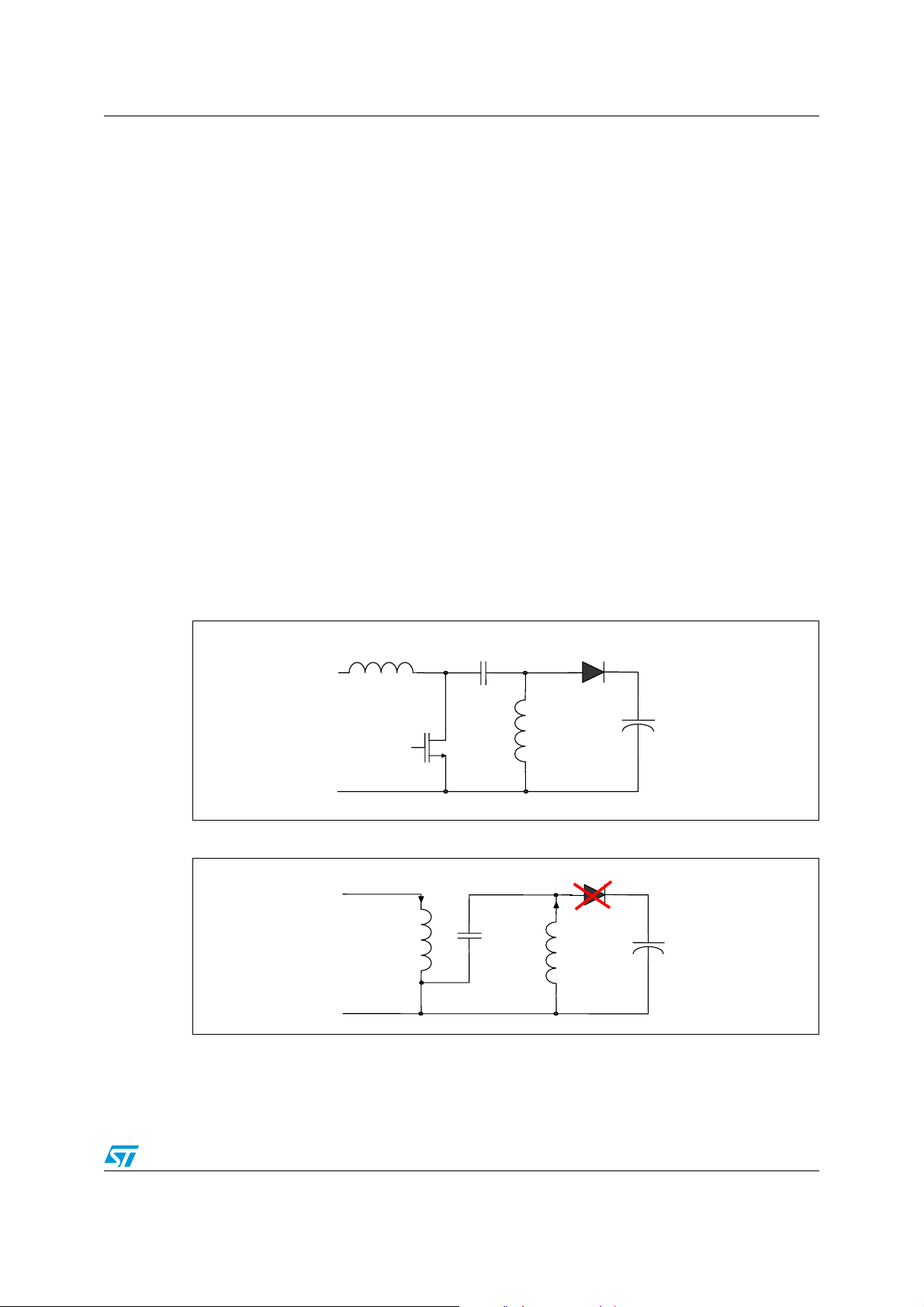
Figure 1. Basic circuit of the sepic converter
C
1
L
2
M
1
D
1
L
1
Figure 2. Sepic converter when the main switch is on
D
1
+
V
IN
-
I
L2
L
2
M
1
-
C
1
VC1=V
+
I
L1
IN
L
1
C
2
+
V
C
2
OUT
-
5/25
Page 6
Sepic topology for PFC converter AN2435
C
IN
IN
T
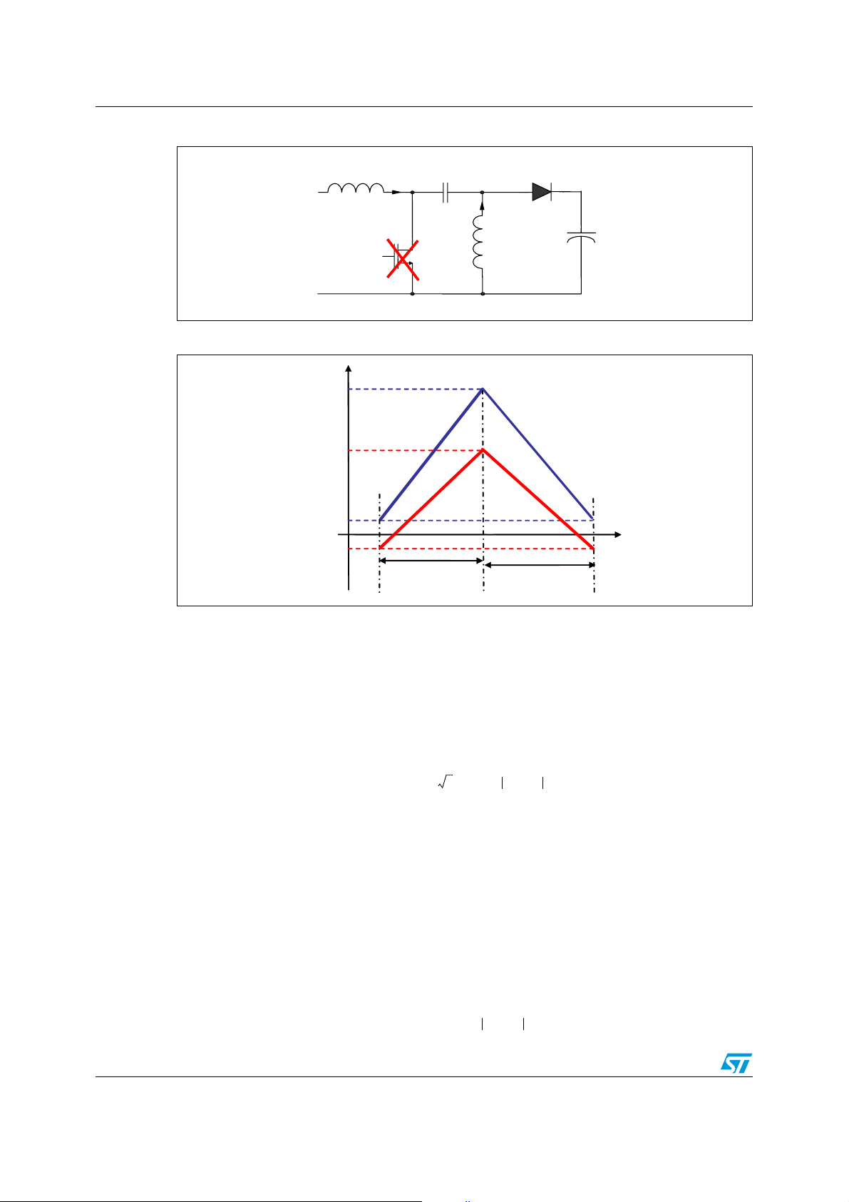
Figure 3. Sepic converter when the main switch is off
D
VC1=V
+ -
+
L
V
-
I
2
L2
1
M
1
I
L1
L
1
+
C
1
2
V
OUT
-
Figure 4. Inductor L1 and inductor L2 current waveform
I
L1_pk
IL1(t)
I
L2_pk
I
L1_0
I
L2_0
T
on
off
t
1.2 Sepic converter as a PFC circuit operating in transition mode [1.]
In PFC applications, input voltage is the rectified main and it changes according to the
equation:
Equation 5
IL2(t)
VINϑ() 2V
where ϑ is 2 πf
, fL is the line frequency, and Vac is the rms value of the line voltage.
L
As switching frequency is in the range of some tenth of kHz, and thus much higher than the
line frequency, we can assume ϑ is constant over each switching cycle.
The L6562 (see [2]) is a current mode controller dedicated to PFC applications. It is used in
this instance. It senses the MOSFET current and the input voltage of the converter (rectified
main), through a sense resistor and a resistor divider respectively. Cycle by cycle the
MOSFET is switched-off as the sensed current reaches a limit set by the controller. This limit
is proportional to the sensed input voltage so, the MOSFET peak current (I
sinusoidal reference:
•ϑ()sin•=
ac
(t)) follows a
PK
Equation 6
IPKt() I
PK
6/25
ϑ()sin•=
Page 7

AN2435 Sepic topology for PFC converter
Taking into account that input voltage is now the rectified main, Equation 1 and Equation 2
can be rewritten as follows:
Equation 7
IL1t ϑ,()I
L10
VINϑ()
------------------
L
1
tIL2t ϑ,(),• I
L20
VINϑ()
------------------
L
2
t•+=+=
Due to transition mode operation, the MOSFET is switched on as soon as the diode current
falls to zero. This means that:
Equation 8
I
– 0=
L10IL20
From and Equation 8, the MOSFET peak current equation may be derived:
Equation 9
1
1
⎛⎞
ϑ()
----- -
----- -+
I
PK
⎝⎠
L
1
tONϑ()• 2• Vac•ϑ()sin•=
L
2
Combining Equation 9 and Equation 6 an expression for T
Equation 10
I
PK
1
----- -+
L
1
2
where L
tONϑ()
is the parallel between inductor L1 and inductor L2. Equation 10 indicates that, as
e
----------------------------------------------------------------------------- -
1
⎛⎞
----- -
⎝⎠
L
in TM (Transition Mode) boost converter T
The expression for T
is obtained in a similar way to above:
OFF
ϑ()sin•
2V
ac
is independent from ϑ.
ON
ϑ()sin•••
Equation 11
where V
Once T
ϑ()
T
---------------------------------------------------------------- -=
T
OFF
is the output voltage. The off time is dependent on θ, as in TM boost converter.
O
ON
and T
are known, switching frequency (fSW) may be easily calculated as it is a
OFF
ON
2V
ac
V
O
function of ϑ:
Equation 12
1
fSWϑ()
---------------------------------------- -
T
ONTOFF
---------------------------------------------------------------------------------- -==
ϑ()+
⎛⎞
1
------------------------------------------------- -+
•
T
⎜⎟
ON
⎝⎠
may be obtained:
ON
L
•
eIPK
---------------------- -
2V
•
ac
===
ϑ()sin•••
1
2V
ac
V
O
T
ON
ϑ()sin••
Figure 5 shows the switching frequency versus θ for two different input voltages. To
calculate input current averaged over one switching cycle, Equation 13, the charge balance
on capacitor C1, is used:
Equation 13
V
ϑ()
1
-- -
2
⎛⎞
I
L10
⎝⎠
ϑ()
IN
------------------
L
1
••+
T
ON
TON• I
⎛⎞
ϑ()
L20
⎝⎠
1
-- -
2
V
ϑ()
IN
------------------
L
2
••+
T
ON
T
•ϑ() Q ϑ()==
OFF
7/25
Page 8

Sepic topology for PFC converter AN2435
where Q (ϑ) indicates the quantity of electrical charge that flows through capacitor C1, cycle
by cycle.
Combining Equation 8 and Equation 13, I
(ϑ) may be calculated as follows:
L2(0)
Equation 14
f
Using equation 14, I
ϑ() VINϑ()• TON•
SW
I
L20
L2avg
-------------------------------------------------------------
ϑ()
2
may then be calculated using Equation 15:
T
ON
---------- -
L
T
ϑ()
OFF
---------------------- -–•=
1
L
2
Equation 15
V
I
L2avg
ϑ()
1
-- -
2
ϑ()
IN
------------------
• T
L
2
• I
ON
L20
ϑ()
1
-- -
2
------------------------------------------------------- -
IPK•
•=+=
------------------------
1
2V
•
AC
V
O
ϑ()sin
ϑ()sin+
Equation 15 shows that the input current is not exactly sinusoidal. A certain amount of
distortion is related to the quantity K
Figure 6 shows the input currents (before the bridge diodes) for different values of V
first input current, I
(θ), is calculated for Kv= 0. It is used only as a reference, because it is
0
completely sinusoidal. In this instance, V
current, I
(θ), is at V
1
= 265 V and the third, I2(θ), is the input current at V
AC
, which is defined as follows:
v
2V
×
K
V
is considered to be 200 V. The second input
O
AC
-------------------------=
V
O
= 175 V. All
AC
AC
. The
currents are normalized in accordance with their respective RMS values. In figure 6, the
distortion of the current with respect to a perfect sinusoid is obvious. Even though such
distortion is present, quite high values for the power factor are obtained. The voltage across
capacitor C1 averaged over one switching cycle is the same as the input voltage. There is
an additional voltage ripple due to the currents of the inductors across capacitor C1. Its
amplitude (∆V
(ϑ)) is calculated below:
C1
Equation 16
V
IN
VC1ϑ()∆
8/25
-------------------------------------- -
ϑ() T
•
C
1Le
2
•
ON
T
ϑ()
OFF
---------------------------------------- -
•=
T
ONTOFF
ϑ()+
Page 9

AN2435 Sepic topology for PFC converter
Substituting the values of T
∆VC1 (
ϑ) may be expressed as follows:
(Equation 10), T
ON
(Equation 11), and VIN(θ) (Equation 5),
OFF
Equation 17
2
I
L
e
PK
------- -
---------- -
VC1ϑ()∆
C1
•
-------------------------------------------------------------------- -
•=
2
V
2V
O
ac
2
ϑ()sin
ϑ()sin••+()
It is useful to rewrite some quantities calculated earlier, in terms of converter output power,
RMS input voltage (V
) , and expected efficiency (η), because these quantities are
AC
generally known at the beginning of a design. Input power may be expressed as follows:
Equation 18
1
--- -
f
Pinf
L
I
PK
--------
• dt•=
L
∫
0
----------------------------------------------------------
1K
2
2πf
t•()sin
L
v
2πfLt•()sin•+
2V
ac
2πfLt•()sin••••
(F(Kv)) may be calculated as follows:
Equation 19
1
--- -
f
Fkv() f
L
• dt•=
L
∫
0
2
---------------------------------------------------------
1k
2πfLt•()sin
v
2πfLt•()sin•+
I
may be expressed as follows:
PK
Equation 20
2P
•
ac
O
Fkv()•••
I
PK
--------------------------------------------------- -=
η 2V
The switching frequency can be expressed as:
Equation 21
2
η V
• Fkv()•
fswϑ()
-------------------------------------------------------------------------=
P
OLe
ac
• 1k
v
ϑ()sin•+()•
Figure 5. Switching frequency variation vs θ for two different input voltages
1. Where V
acmin
= 175 V, V
= 265 V, Le = 1 mH, h = 0.9, and PO = 65W.
acmax
9/25
Page 10

Sepic topology for PFC converter AN2435
Figure 6. Input current in TM for sepic PFC
1.3 Coupled inductor sepic converter and ripple steering
If the two inductors are wounded in the same magnetic core, it is possible to reuse the
equations used in Section 1.2. Moreover, the current ripple in the input inductor L
theoretically be reduced to zero, simply by selecting the correct turn ratio. A model of two
coupled inductors is shown in Figure 8. L
lk1
and L
are the leakage inductances, LM is the
lk2
magnetizing inductance and n is the turn ratio.
can
2
The equations that describe the coupled inductor model of Figure 8 are given below.
Equation 22
⎧
⎪
v1t() L
⎪
⎪
⎪
v
⎨
2
⎪
⎪
⎪
⎪
⎩
t() L
L1
dI2t()
-------------- - nL
L2
dI
dI
M
---------
------- - n
dt
dI1t()
-------------- - L
dt
dt
1
dt
•+=
•+•=
M
M
dI
2
-------------- -
dt
dIMt()
--------------- -
dt
dIMt()
--------------- -
••+•=
t()
dt
In the first two sub equations of Equation 22, the derivate of the magnetizing current (I
be substituted with the value given in sub-equation 3.
Considering that the same voltage is applied to both inductors we have:
Equation 23
⎧
⎪
t() L
v
1
⎪
⎨
⎪
v2t() L
⎪
⎩
EQ1
EQ2
dI1t()
-------------- -
•=
dI2t()
-------------- -
•=
dt
dt
Equation 24
EQ1
EQ2
LL1LL2LMLL2n2LMLL1••+•+•
---------------------------------------------------------------------------------------------- -=
LL1LL2LMLL2n2LMLL1••+•+•
---------------------------------------------------------------------------------------------- -=
L
nn1–()LM••+
L2
L
n1–()Lm•–
L1
⎧
L
⎪
⎪
⎨
⎪
⎪
L
⎩
) can
M
10/25
Page 11

AN2435 Sepic topology for PFC converter
C
The main conclusion of Equation 23 and Equation 24, is that the same equations can be
used for coupled and uncoupled inductors. If no current flows on the secondary side, voltage
V
is the same as voltage V
2
1
(see Figure 8) and may be written as follows:
2
Equation 25
V2V
1
2
nV
• n
1
1
L
------------------------- -
• V1•===
LML
+
M
LK1
As the same voltage is applied, simultaneously, to both inductors in a sepic converter,
Equation 25 may be simplified below as:
Equation 26
L
M
------------------------- -
n
• 1=
LML
+
LK1
When the above ‘ripple steering’ condition is verified theoretically, the voltage across L
LK2
is
zero and no current flows on the secondary side. In the actual circuit only the high frequency
components of the inductor L2 current are attenuated. Once Equation 26 is verified,
Equation 24 may be simplified as:
Equation 27
L
⎧
EQ1LMLLK1
⎨
L
⎩
EQ2
+=
∞=
Therefore, for a sepic converter with coupled inductors, infinite inductance at the input may
be seen theoretically once Equation 26 is satisfied. In the actual circuit, due to imperfect
matching with Equation 26 and due to the fact that the voltages applied to the two inductors
are not exactly the same (because of the voltage ripple on capacitor C1), a large input
inductance may be seen at the converter input. This input inductance helps the line filter in
eliminating the switching frequency component of the input current.
Figure 7. Coupled inductor of a sepic converter
D
1
L
2
L
M
1
1
C
1
2
Figure 8. Model of two coupled inductors
L
lk1
+
V
1
I
1
I
M
+
1
V
1
1 : n
L
M
I
+
L
2
V
lk2
+
1
2
V
2
-
-
-
-
11/25
Page 12

Sepic topology for PFC converter AN2435
1.4 Small signal model for a TM sepic converter
It is possible to model the output stage of the sepic converter as a current source. The
sourced current is a function of the input voltage RMS value, the output voltage, and the
MOSFET peak current. To obtain the necessary function, the output diode current may first
by averaged over each switching cycle, to give the following equation:
Equation 28
2
ϑ()sin()
ϑ()sin•+
• F
•=
PK
•
2V
⎛⎞
⎜⎟
⎝⎠
ACRMS
----------------------------------- -
V
O
ID1ϑ()
k
------------- -
I
vmin
----------------------------------------- -
•=
2
1k
PK
•
v
Assuming that the control loop reaction must be very slow to remain constant over a single
line cycle, then to ensure high PFC, Equation 28 may be averaged with respect to θ as
follows:
Equation 29
2V
•
I
DlavgVACRMSVOIPK
,,()
1
-- -
• I
2
ACRMS
----------------------------------- -
V
O
For small variations of its argument, the I
function may be approximated with a linear
D1AVG
function, and the output stage of the sepic converter may be represented by the circuit in
Figure 10. Bearing in mind that F(K
Figure 10), e
(see Figure 10) and r2 (see Figure 10) are given below:
2
) was defined in Equation 19, expressions for g2 (see
v
Equation 30
∂I
---------------------- -=
2
∂I
PK
I
PK
•
O
-------------------------=
V
D1AVG
ACRMS
1
-- -
• FKv()•==
K
v
2
⎛⎞
KvFKv()K
••
⎝⎠
2V
×
AC
V
O
∂FKv()
------------------
•+
v
∂K
1–
v
∂I
D1AVG
--------------------- -
r
2
∂V
O
It should be remembered that K
Also, note that g
is not calculated here because is not used in the control Loop design.
2
g
∂I
D1AVG
--------------------- -
e
2
∂I
1–
---------------- -
=–=
2V
was defined as:
v
K
Then, using Figure 10 and the sub-equations of Equation 30, it is possible to deduce the
small signal transfer function (control to output) G
(S)
= V
COMP
(s)/VO(s).
Equation 31
Gs()
ˆ
∂V
--------------------- ˆ
∂V
COMP
G
O
O
--------------- -==
s
1
----- -+
ω
P
where the gain (G
) and the pole frequency (ωP) are defined below:
O
Equation 32
2V
GOKPKM• e2•
where (R
) is the assumed resistive load.
O
12/25
---------------------------------
•
•
R
SENSE
•
ACrms
r
2RO
------------------ -
•ω
r
+
2RO
r2RO–
--------------------------------=,=
P
• RO•
C
2r2
Page 13

AN2435 Practical design example of a sepic converter
Figure 9. Equivalent current source of the sepic converter
I
D1AVG
Load
C
1
Figure 10. Small signal model for the TM sepic converter
+
ˆ
Vg
⋅
ACRMS
2
ˆ
Ie
⋅
Pk
2
r
2
Load
C
2
ˆ
V
O
-
2 Practical design example of a sepic converter
A practical example of a sepic converter is described below.
2.1 Design specifications
For the input data, the design specifications are needed.
Table 1. Design specification
Quantity Value
Mains voltage range: V
INMIN (RMS)
– VI
NMAX (RMS)
Regulated DC output voltage 200 V
Rated Output Power: P
Minimum switching frequency: f
Maximum over-voltage admitted: ∆V
Maximum output voltage ripple ∆V
65 W
O
swmin
OVP
O
Expected efficiency: η 90 %
Maximum mains RMS current
175 V
I
INRMSMAX
- 265 V
ACRMS
ACRMS
45 kHz
40 V
20 V
P
O
---------------------------- 420m A==
η V
•
ACMIN
13/25
Page 14

Practical design example of a sepic converter AN2435
Table 1. Design specification (continued)
Quantity Value
P
O
I
------- 325mA==
Rated output current: I
O
Output equivalent resistor
O
I
O
V
O
2
V
O
---------- 615Ω==
P
O
The complete schematic of the circuit is given in Figure 13.
2.2 MOSFET (M1) selection
The MOSFET peak current value (IPK) is calculated using Equation 18. Substituting the
quantities given in the electrical specifications, the MOSFET peak current value is
I
= 2.36 A. The RMS value of the current flowing through the MOSFET may be calculated
PK
using Equation 33:
Equation 33
FK
()
vmin
----------------------- - 0.678A==
3
where:
I
M1RMSIPK
Equation 34
Under the worst case scenario, the MOSFET and the output diode have to sustain a voltage
that is the sum of the maximum peak input voltage and the maximum output voltage.
Considering the electrical specifications above and a safety margin of 10%, the minimum
breakdown voltage (B
DVSSMin
Equation 35
B
DVSSMin
2V
ACmaxVO
To avoid large heat sink, the RMS value of the through current suggests using a MOSFET
with an R
maximum R
not greater than 1.5 Ω. The selected MOSFET, the STP9NK70, has a
DSON
of 1.2 Ω at 25 °C and a breakdown voltage of 700 V.
DSON
2.3 Diode D1 selection
The average value of the diode D1 current is the output current . The RMS value of the
current flowing through diode D1 can be calculated using the following formula:
Equation 36
I
D1RMSIPK
K
vmin
) for M1 is:
1
1
-- -
-- -
•• 0.687A==
∫
3
π
2V
•
ACMIN RMS()
-------------------------------------------------=
V
∆++•()1.1• 375V 200V 40V++()1.1• 677V===
OVP
π
0
V
O
K
•
vmin
------------------------------------------------------
vmin
•+
1K
3
ϑ()sin
ϑ()sin
ϑd•
3
14/25
Page 15

AN2435 Practical design example of a sepic converter
The minimum breakdown voltage of diode D1 is the same as for the MOSFET. The selected
diode D1, STTH208, has a breakdown voltage of 800 V. When it is forward biased, the
voltage drop, (V
) is 1.05 V and the dynamic resistance( rd) is 100 mΩ. The power
d
dissipation on DI may easily be calculated as follows:
Equation 37
P
D1Loss
VdIO• rdI
• 0.388W=+=
2
D1RMS
2.4 Capacitor C1 selection
The equivalent inductance Le must be calculated, using Equation 38 and knowing the
minimum switching frequency, the output power, and the efficiency from previous electrical
specifications:
Equation 38
2
η V
ACMIN RMS()
--------------------------------------------------------------------------- -
L
e
P
Ofswmin
The value of capacitor C1 may be selected by imposing the maximum voltage ripple across
it. Considering a maximum voltage ripple of 15 V
Fk
()••
1k
+()••
vmin
vmin
1041m H 1mH≅==
∆V
C1MAX
and using Equation 21, the following formula may be calculated:
15V=
Equation 39
2
C
1
L
------------------------ -
V
∆
C1MAX
I
e
•
PK
---------- -
2
A 470 nF capacitor was selected.
It is important to note that the voltage ripple on capacitor C1 will affect the ripple steering
effect.
The difference between the voltages across the two inductors, either when the MOSFET is
on or off, is the difference between the voltage on capacitor C1 and the input voltage, which
effectively is the switching frequency voltage ripple, across capacitor C1.
Because of this ripple, the two inductors do not have exactly the same voltage. Even when
Equation 26 is perfectly satisfied, the current ripple on the input inductor L2 is not zero.
2.5 Output capacitor C2 selection
The output diode current, averaged over each switching cycle, is given in Equation 29. The
graph of this waveform is shown in Figure 11 The quantity of electrical charge that goes into
capacitor C2 is the same as the integral of the diode current:
Equation 40
C2VOϑ()• X ϑ() ID1α() αd•
-------------------------------------------------- -
V
1
2V
•+()
O
==
acmin
ϑ
∫
0
416nF=•=
15/25
Page 16

Practical design example of a sepic converter AN2435
Under steady state conditions, the output voltage is maximum and minimum at the two
points where I
(θ) equals the output current IO. Letting these angles be θ1 and θ2, the
D1
minimum output capacitor value that guarantees an output voltage ripple lower than the
specified ∆V
is:
O
Equation 41
X ϑ1()X ϑ2()–
-----------------------------------------=
C
2
2 π f
VO∆•••
L
2.6 Transformer design
The selected magnetic core is an ETD29 made with N67 material. The effective area (Ae) of
this core is 0.76 cm
2
. Once the core is selected, the minimum turn number, which prevents
the transformer from saturation or overheating, may be calculated using the formula:
Equation 42
VinTON•
min
-------------------------=
A
Bƥ
e
N2
The maximum magnetic swing (∆B) selected is 0.25 T. In the current design the number of
turns for the inductor L2 is 125.
If the ripple steering condition is satisfied, Equation 43 (below) may be calculated using
Equation 24:
Equation 43
-------------+
L
1
EQ2
1–
L
LK1LMLOP1
OP1
=+==
is the inductance measured at the
1
⎛⎞
L
-------------
e
⎝⎠
L
EQ1
It may be used to select the proper air gap, where L
primary side with the secondary side open. Selecting the correct turn ratio to meet the ripple
steering condition for an actual transformer (rather than a theoretical one) is not easy, as the
internal parameters of the transformer (L
equivalent to Equation 26 but is based on measurable quantities. L
and L
M
) are unknown. Equation 44 is
LK1
SH1
and L
OP1
are the
primary inductances, measured when the secondary side is shorted and when the
secondary side is open, respectively.
Equation 44
n
Equation 44 is obtained using the hypothesis expressed in Equation 45:
Equation 45
L
Equation 45 is generally true if the transformer has a ‘symmetrical structure’. Figure 12
shows two examples of transformers with a symmetrical structure. A slotted transformer
(Figure 12 b) is used in the board for the current document. The selected turn ratio (n) is
1.28, which gives a value of 98 turns for the inductor L1.
16/25
LK1
L
OP1
-------------------------------- -=
L
–
OP1LSH1
1
----- -
L
•=
2
n
LK2
Page 17

AN2435 Practical design example of a sepic converter
2.7 Selection of other components
Selection of the other components of the circuit may be made using the guidelines for a
boost converter which are given in [2 ]. Capacitor C1 must be considered in parallel with the
input capacitor, which means that a small capacitor of 10 nF is adequate for the current
design.
For the control loop design the procedure used for a boost converter in [4 ] may be followed.
The small signal model developed in this document must be considered.
The charge pump which supplies the IC, while respecting the calculated steady state
values, needs to be a little over-sized. During start-up, capacitor C2 is not pre-charged by
the inrush current as in a boost converter, and therefore, the charge pump provides less
current. In order not to have too big a charge pump, the capacitor on the V
L6562 has to be increased during start up phase to supply the IC, even if the charge pump
is not able to provide enough current.
Figure 11. Output diode current averaged over the switching cycles
pin of the
CC
Figure 12. Transformers with symmetrical structures
Primary Wi nding
Secondary Winding
Primary Winding
a
Secondary Winding
b
17/25
Page 18

Conclusion AN2435
3 Conclusion
This document presented the sepic converter operating in transition mode for power factor
correction applications. The ripple steering technique was also presented. The basic theory
behind the sepic converter and the ripple steering technique was discussed and design
equations were outlined. An example of a design was proposed.
3.1 References
1. Analysis and design of SEPIC converter in boundary conduction mode for universal-
line power factor correction applications. From Power Electronics Specialists
Conference, 2001. PESC. 2001 IEEE 32nd Annual.
2. L6561, enhanced transition mode power factor corrector (AN966).
3. Minimize filtering with ripple steering. Published in Analog Zone.
4. Control loop modeling of L6561-based TM PFC (AN1089)
5. Transition-mode PFC controller (L6562 datasheet)
4 Board description and bench evaluation results
4.1 Board description
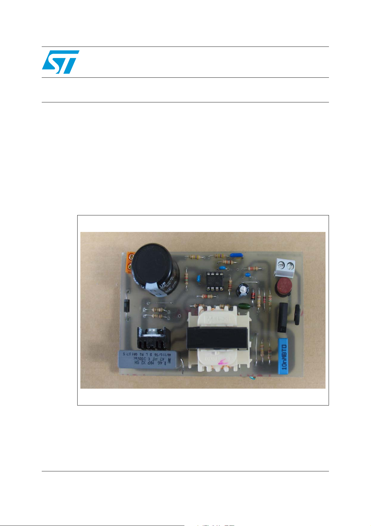
This section gives the bill of material and the schematic of the board according to the
electrical specifications given in Section 2.
Table 2. Bill of material
Part Value Description
C1 470 nF 630 V capacitor
C2 68 µF 250 V electrolitic capacitor
C3 10 nF X2 type capacitor
C4 47 µF 25V electrolitic capacitor
C5 56 nF 100 V capacitor
C6 47 nF Samll signal capacitor
C7 10 nF Small signal capacitor
C8 1.5 µF Small signal capacitor
D1 STTH208
D2 BRIDGE 600 V, 1 A standard bridge diode
D3 1N4148 Standard diode
STMicroelectronics
high voltage ultrafast rectifier
D4 15 Vz 15 V zener diode
F1 1 A 1 A fuse
18/25
Page 19

AN2435 Board description and bench evaluation results
Table 2. Bill of material (continued)
Part Value Description
NTC1 1 1 Ohm NTC
Q1 STP9NK70
R1a, R1b 1 Ohm 1 % precision resistor
R2, R3 470 Kohm 1 % precision resistor
R4 12 Kohm 1 % precision resistor
R5 22 Ohm Resistor
R6 12 Kohm Resistor
R7, R8 1.2 Megaohm Resistor
R9 8.2 Kohm Resistor
R10 18 Kohm Resistor
R11 82 Ohm Resistor
R13,R12 270 Kohm Resistor
T1 Coupled inductors
U1 L6562 Transition mode PFC controller
N-Channel 700 V supermesh
STMicroelectronics
tm
power MOSFET
19/25
Page 20

Board description and bench evaluation results AN2435
Figure 13. Schematic of the sepic converter
J1
1
2
CON2
D1 STTH208
R2
9
3
470k
13 C1
5
R3
470k
C2
68uF
470nF
T1
Coupled Induc tors
7
1
M1
STP9NK70
23
1
R522
C5 56nF
R11 82
R4
12k
R1a
1 1/4W
R1b
1 1/4W
1 2
D4
15Vz
C4 47uF
D3
1N4148
R6
12k
8
7
6
5
GD
Vcc
INV
U1
1
ZCD
GND
COMP
MUL T
2
3
L6562
CS
4
R12
270k
R13
R7
1.2 Meg
4
BRID GE
NTC1
2
D2
-+
1
F1
1A
1
3
20/25
270k
47nF
C6
C7
10nF
R10
10nF
18k
R9
8.2k
C8
1.5 uF
R8
1.2 Meg
C3
1
2
J2
CON2
Page 21

AN2435 Board description and bench evaluation results
4.2 Bench results
The diagrams in this section summarize the results of certain bench evaluations. They also
show waveforms under different load and line conditions.
Figure 14 illustrates the measured efficiency for different loads (65 W, 38 W and 22 W of
output power) versus the input ac voltage.
Figure 15 demonstrates the MOSFET drain voltage (Ch4), the output voltage (Ch3) and the
input voltage.
The quantities that indicate the quality of the input current as power factor, THD (Total
Harmonic Distortion) and crest factor, where measured at full load and for different input
voltages. They are reported in Ta bl e 3 .
Figure 16 to Figure 19 show the currents flowing in the two inductors (Ch1: L1 current; Ch2:
L2 current) for different load conditions. Letting the input voltage of the converter (the
rectified main) be a perfect rectified sinusoid, it may be used as a reference and is shown as
Ch4 in the above figures.
Figure 20 illustrates the input current (Ch1) measured before the input bridge diodes. The
voltage at the input of the bridge diodes (Ch4) is also shown as a reference.
Figure 20 is input current at full load (65 W) with 230 V
current at half load (32 W) with 230 V
Table 3. Input current quality measurements
Input voltage (V
175 0.992 10.3 1.35
220 0.986 12.3 1.36
230 0.984 12.6 1.37
265 0.975 14.2 1.46
) PFC THD % Crest factor
RMS
as input voltage.
ac
P
= 65 W
out
Figure 14. Efficiency chart
as input voltage. Figure 21 is input
ac
21/25
Page 22

Board description and bench evaluation results AN2435
Figure 15. Main waveform of the circuit
1. Test conditions include P
= 65 W and Vin = 230 V
out
ACRMS
.
22/25
Page 23

AN2435 Board description and bench evaluation results
Figure 16. Current of the inductors over one
line cycle: V
P
= 65 W
out
= 230 V
in
ACRMS
,
Figure 18. Current of the inductors over one
line cycle: V
P
= 65 W
out
= 230 V
in
ACRMS
,
Figure 17. Current of the inductors over
switching cycles: V
P
= 65 W
out
= 230 V
in
ACRMS
Figure 19. Currents of the inductors over
switching cycles: V
P
= 65 W
out
= 230 V
in
ACRMS
,
,
23/25
Page 24

Revision history AN2435
Figure 20. Input current: 230 Vac input, 65 W
output
5 Revision history
Table 4. Revision history
Figure 21. Input current: 230 Vac input, 32 W
output
Date Revision Changes
05-Mar-2007 1 First issue
24/25
Page 25

AN2435
Please Read Carefully:
Information in this document is provided solely in connection with ST products. STMicroelectronics NV and its subsidiaries (“ST”) reserve the
right to make changes, corrections, modifications or improvements, to this document, and the products and services described herein at any
time, without notice.
All ST products are sold pursuant to ST’s terms and conditions of sale.
Purchasers are solely responsible for the choice, selection and use of the ST products and services described herein, and ST assumes no
liability whatsoever relating to the choice, selection or use of the ST products and services described herein.
No license, express or implied, by estoppel or otherwise, to any intellectual property rights is granted under this document. If any part of this
document refers to any third party products or services it shall not be deemed a license grant by ST for the use of such third party products
or services, or any intellectual property contained therein or considered as a warranty covering the use in any manner whatsoever of such
third party products or services or any intellectual property contained therein.
UNLESS OTHERWISE SET FORTH IN ST’S TERMS AND CONDITIONS OF SALE ST DISCLAIMS ANY EXPRESS OR IMPLIED
WARRANTY WITH RESPECT TO THE USE AND/OR SALE OF ST PRODUCTS INCLUDING WITHOUT LIMITATION IMPLIED
WARRANTIES OF MERCHANTABILITY, FITNESS FOR A PARTICULAR PURPOSE (AND THEIR EQUIVALENTS UNDER THE LAWS
OF ANY JURISDICTION), OR INFRINGEMENT OF ANY PATENT, COPYRIGHT OR OTHER INTELLECTUAL PROPERTY RIGHT.
UNLESS EXPRESSLY APPROVED IN WRITING BY AN AUTHORIZED ST REPRESENTATIVE, ST PRODUCTS ARE NOT
RECOMMENDED, AUTHORIZED OR WARRANTED FOR USE IN MILITARY, AIR CRAFT, SPACE, LIFE SAVING, OR LIFE SUSTAINING
APPLICATIONS, NOR IN PRODUCTS OR SYSTEMS WHERE FAILURE OR MALFUNCTION MAY RESULT IN PERSONAL INJURY,
DEATH, OR SEVERE PROPERTY OR ENVIRONMENTAL DAMAGE. ST PRODUCTS WHICH ARE NOT SPECIFIED AS "AUTOMOTIVE
GRADE" MAY ONLY BE USED IN AUTOMOTIVE APPLICATIONS AT USER’S OWN RISK.
Resale of ST products with provisions different from the statements and/or technical features set forth in this document shall immediately void
any warranty granted by ST for the ST product or service described herein and shall not create or extend in any manner whatsoever, any
liability of ST.
ST and the ST logo are trademarks or registered trademarks of ST in various countries.
Information in this document supersedes and replaces all information previously supplied.
The ST logo is a registered trademark of STMicroelectronics. All other names are the property of their respective owners.
© 2007 STMicroelectronics - All rights reserved
STMicroelectronics group of companies
Australia - Belgium - Brazil - Canada - China - Czech Republic - Finland - France - Germany - Hong Kong - India - Israel - Italy - Japan -
Malaysia - Malta - Morocco - Singapore - Spain - Sweden - Switzerland - United Kingdom - United States of America
www.st.com
25/25
 Loading...