

Page 1
AN2432
Application note
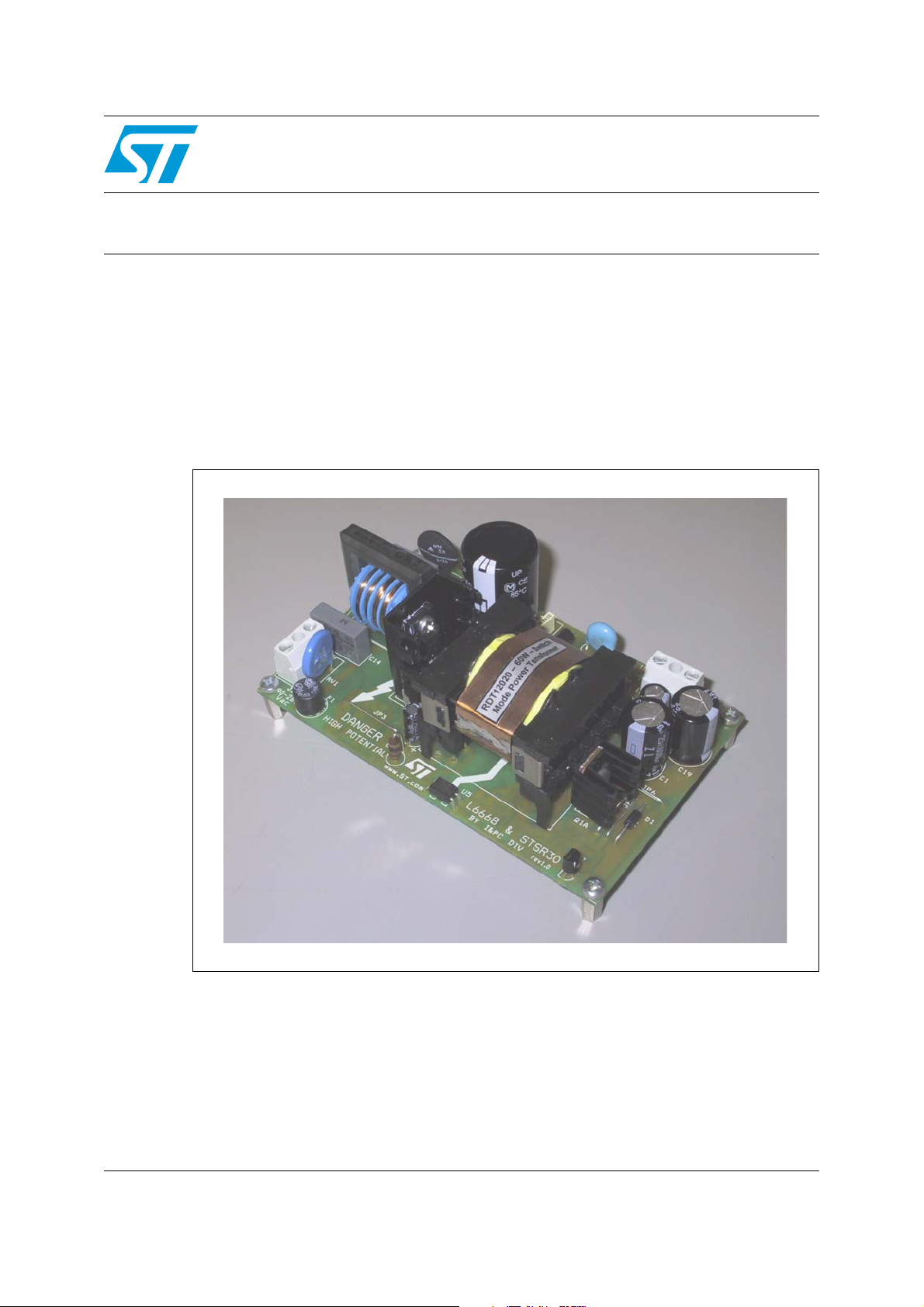
EVALSTSR30-60W: 60W AC-DC Adapter
with synchronous rectification using L6668 and STSR30
Introduction
This document describes a 60W adapter application using the L6668 fixed frequency
current mode PWM controller and the STSR30 smart driver for flyback synchronous
rectification.
This chipset guarantees low no-load consumption and high efficiency, making it easy to
comply with world-wide mandatory and voluntary energy saving requirements.
EVALSTSR30-60W demo board
October 2006 Rev 2 1/27
www.st.com
Page 2

AN2432 Contents
Contents
1 Adapter features . . . . . . . . . . . . . . . . . . . . . . . . . . . . . . . . . . . . . . . . . . . . 5
1.1 Main characteristics . . . . . . . . . . . . . . . . . . . . . . . . . . . . . . . . . . . . . . . . . . 5
1.2 Circuit description . . . . . . . . . . . . . . . . . . . . . . . . . . . . . . . . . . . . . . . . . . . . 5
2 Electrical performance . . . . . . . . . . . . . . . . . . . . . . . . . . . . . . . . . . . . . . 10
3 Functional check . . . . . . . . . . . . . . . . . . . . . . . . . . . . . . . . . . . . . . . . . . . 13
3.1 Start-up behavior at full load . . . . . . . . . . . . . . . . . . . . . . . . . . . . . . . . . . 13
3.2 Wake-up time . . . . . . . . . . . . . . . . . . . . . . . . . . . . . . . . . . . . . . . . . . . . . . 13
3.3 Power-down . . . . . . . . . . . . . . . . . . . . . . . . . . . . . . . . . . . . . . . . . . . . . . . 14
3.4 Short-circuit tests . . . . . . . . . . . . . . . . . . . . . . . . . . . . . . . . . . . . . . . . . . . 15
3.5 Overvoltage protection . . . . . . . . . . . . . . . . . . . . . . . . . . . . . . . . . . . . . . . 15
4 Conducted noise measurements (pre-compliance test) . . . . . . . . . . . 17
5 Thermal measurements . . . . . . . . . . . . . . . . . . . . . . . . . . . . . . . . . . . . . 18
6 Bill of materials . . . . . . . . . . . . . . . . . . . . . . . . . . . . . . . . . . . . . . . . . . . . 20
7 PCB layout . . . . . . . . . . . . . . . . . . . . . . . . . . . . . . . . . . . . . . . . . . . . . . . . 23
8 Transformer specification . . . . . . . . . . . . . . . . . . . . . . . . . . . . . . . . . . . 24
8.1 Electrical characteristics . . . . . . . . . . . . . . . . . . . . . . . . . . . . . . . . . . . . . . 24
8.2 Mechanical aspect . . . . . . . . . . . . . . . . . . . . . . . . . . . . . . . . . . . . . . . . . . 25
9 Revision history . . . . . . . . . . . . . . . . . . . . . . . . . . . . . . . . . . . . . . . . . . . 26
2/27
Page 3

List of figures AN2432
List of figures
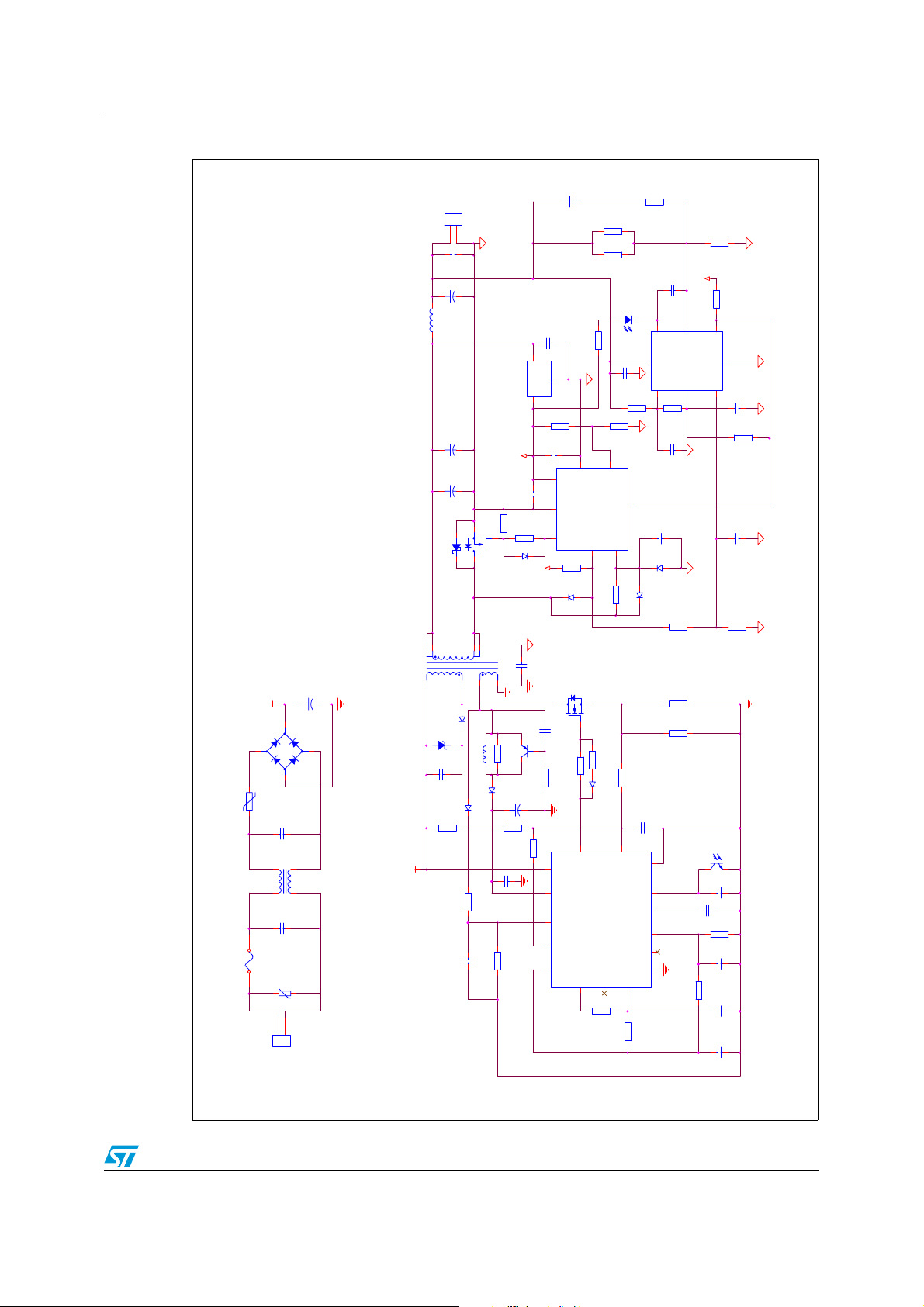
Figure 1. Electrical diagram . . . . . . . . . . . . . . . . . . . . . . . . . . . . . . . . . . . . . . . . . . . . . . . . . . . . . . . . 6
Figure 2. VIN = 115VRMS - 60Hz . . . . . . . . . . . . . . . . . . . . . . . . . . . . . . . . . . . . . . . . . . . . . . . . . . . . 8
Figure 3. VIN = 230VRMS - 50Hz . . . . . . . . . . . . . . . . . . . . . . . . . . . . . . . . . . . . . . . . . . . . . . . . . . . . 8
Figure 4. VIN = 115VRMS - 60Hz . . . . . . . . . . . . . . . . . . . . . . . . . . . . . . . . . . . . . . . . . . . . . . . . . . . . 8
Figure 5. VIN = 230VRMS - 50Hz . . . . . . . . . . . . . . . . . . . . . . . . . . . . . . . . . . . . . . . . . . . . . . . . . . . . 8
Figure 6. VIN = 115VAC - CCM . . . . . . . . . . . . . . . . . . . . . . . . . . . . . . . . . . . . . . . . . . . . . . . . . . . . . . 9
Figure 7. CCM - Anticipation detail . . . . . . . . . . . . . . . . . . . . . . . . . . . . . . . . . . . . . . . . . . . . . . . . . . . 9
Figure 8. VIN = 230VAC - DCM . . . . . . . . . . . . . . . . . . . . . . . . . . . . . . . . . . . . . . . . . . . . . . . . . . . . . . 9
Figure 9. DCM - INHIBIT synchronization . . . . . . . . . . . . . . . . . . . . . . . . . . . . . . . . . . . . . . . . . . . . . . 9
Figure 10. Burst mode operation at 230VAC and no load . . . . . . . . . . . . . . . . . . . . . . . . . . . . . . . . . . 11
Figure 11. Start-up at 88VAC - 60Hz . . . . . . . . . . . . . . . . . . . . . . . . . . . . . . . . . . . . . . . . . . . . . . . . . . 13
Figure 12. Start-up at 264VAC - 50Hz . . . . . . . . . . . . . . . . . . . . . . . . . . . . . . . . . . . . . . . . . . . . . . . . . 13
Figure 13. Wake-up at 115VAC - 60Hz . . . . . . . . . . . . . . . . . . . . . . . . . . . . . . . . . . . . . . . . . . . . . . . . 14
Figure 14. Wake-up at 230VAC - 50Hz . . . . . . . . . . . . . . . . . . . . . . . . . . . . . . . . . . . . . . . . . . . . . . . . 14
Figure 15. Power-down at 115VAC - 60Hz . . . . . . . . . . . . . . . . . . . . . . . . . . . . . . . . . . . . . . . . . . . . . 14
Figure 16. Power-down at 230VAC - 50Hz . . . . . . . . . . . . . . . . . . . . . . . . . . . . . . . . . . . . . . . . . . . . . 14
Figure 17. Short circuit at 88VAC - 60Hz . . . . . . . . . . . . . . . . . . . . . . . . . . . . . . . . . . . . . . . . . . . . . . . 15
Figure 18. Short circuit at 264VAC - 50Hz . . . . . . . . . . . . . . . . . . . . . . . . . . . . . . . . . . . . . . . . . . . . . . 15
Figure 19. OVP at 115VAC - full load . . . . . . . . . . . . . . . . . . . . . . . . . . . . . . . . . . . . . . . . . . . . . . . . . 16
Figure 20. OVP at 230VAC - full load . . . . . . . . . . . . . . . . . . . . . . . . . . . . . . . . . . . . . . . . . . . . . . . . . 16
Figure 21. OVP at 115VAC - no load . . . . . . . . . . . . . . . . . . . . . . . . . . . . . . . . . . . . . . . . . . . . . . . . . . 16
Figure 22. OVP at 230VAC - no load . . . . . . . . . . . . . . . . . . . . . . . . . . . . . . . . . . . . . . . . . . . . . . . . . . 16
Figure 23. CE peak measure at 115VAC and full load . . . . . . . . . . . . . . . . . . . . . . . . . . . . . . . . . . . . 17
Figure 24. CE peak measure at 230VAC and full load . . . . . . . . . . . . . . . . . . . . . . . . . . . . . . . . . . . . 17
Figure 25. VIN = 115VAC - full load . . . . . . . . . . . . . . . . . . . . . . . . . . . . . . . . . . . . . . . . . . . . . . . . . . . 18
Figure 26. VIN = 230VAC - full load . . . . . . . . . . . . . . . . . . . . . . . . . . . . . . . . . . . . . . . . . . . . . . . . . . . 19
Figure 27. Silk screen - top side . . . . . . . . . . . . . . . . . . . . . . . . . . . . . . . . . . . . . . . . . . . . . . . . . . . . . 23
Figure 28. Silk screen - bottom side . . . . . . . . . . . . . . . . . . . . . . . . . . . . . . . . . . . . . . . . . . . . . . . . . . 23
Figure 29. Copper tracks . . . . . . . . . . . . . . . . . . . . . . . . . . . . . . . . . . . . . . . . . . . . . . . . . . . . . . . . . . . 23
Figure 30. Transformer electrical diagram . . . . . . . . . . . . . . . . . . . . . . . . . . . . . . . . . . . . . . . . . . . . . . 24
Figure 31. Windings position . . . . . . . . . . . . . . . . . . . . . . . . . . . . . . . . . . . . . . . . . . . . . . . . . . . . . . . . 25
3/10
Page 4

AN2432 List of tables
List of tables
Table 1. Line and load regulation . . . . . . . . . . . . . . . . . . . . . . . . . . . . . . . . . . . . . . . . . . . . . . . . . . . 10
Table 2. Efficiency at 115VRMS . . . . . . . . . . . . . . . . . . . . . . . . . . . . . . . . . . . . . . . . . . . . . . . . . . . . 10
Table 3. Efficiency at 230VRMS . . . . . . . . . . . . . . . . . . . . . . . . . . . . . . . . . . . . . . . . . . . . . . . . . . . . 10
Table 4. No load consumption . . . . . . . . . . . . . . . . . . . . . . . . . . . . . . . . . . . . . . . . . . . . . . . . . . . . . 11
Table 5. Power consumption with 0.5W output . . . . . . . . . . . . . . . . . . . . . . . . . . . . . . . . . . . . . . . . 11
Table 6. Mandatory energy saving requirements (from 1 January 2008) . . . . . . . . . . . . . . . . . . . . . 12
Table 7. Voluntary energy saving requirements (from 1 January 2008) . . . . . . . . . . . . . . . . . . . . . . 12
Table 8. Comparison between standard and SR flyback . . . . . . . . . . . . . . . . . . . . . . . . . . . . . . . . . 12
Table 9. Key components temperature at 115VAC - full load. . . . . . . . . . . . . . . . . . . . . . . . . . . . . . 18
Table 10. Key components temperature at 230VAC - full load. . . . . . . . . . . . . . . . . . . . . . . . . . . . . . 19
Table 11. Part list . . . . . . . . . . . . . . . . . . . . . . . . . . . . . . . . . . . . . . . . . . . . . . . . . . . . . . . . . . . . . . . . 20
Table 12. Winding characteristics . . . . . . . . . . . . . . . . . . . . . . . . . . . . . . . . . . . . . . . . . . . . . . . . . . . . 25
Table 13. Revision history . . . . . . . . . . . . . . . . . . . . . . . . . . . . . . . . . . . . . . . . . . . . . . . . . . . . . . . . . 26
4/10
Page 5

Adapter features AN2432
1 Adapter features
1.1 Main characteristics
The 60W AC-DC adapter board described in this application note has the following main
characteristics:
● Input:
–V
– f: 45 ~ 66 Hz
● Output:
– 12V
● No - Load:
– Pin below 0.3W
● Short circuit: protected with Auto-Restart feature
● PCB type and size:
–FR4
– Single side: 70 µm
– 120 x 75 mm
● Safety: according to EN60065
● EMI: Compliance with EN55022 - Class B specifications
: 88 ~ 264 V
IN
± 2% - 5A
DC
RMS
1.2 Circuit description
This circuit implements a flyback transformer which is a very popular topology for this kind of
application and power level, thanks to its simplicity and good trade-off between cost and
performance. To improve the converter's efficiency, the EVALSTSR30 demo board uses
synchronous rectification.
The converter works in both Continuous and Discontinuous conduction mode depending on
the input voltage (the circuit has a wide input voltage range) and the output load. The
68-kHz switching frequency provides a good compromise between the transformer size and
the harmonics of the switching frequency, optimizing input filter.
The input section includes protection elements (varistor, fuse and NTC for inrush current
limiting), a standard Pi-filter for EMC suppression, a bridge and an electrolytic bulk capacitor
as the front-end AC-DC converter. The transformer is a layer type, uses a standard ETD34
ferrite core and is designed to have a reflected voltage of 95V. The power MOS is a 700V 1Ω and a transil clamp network is used for leakage inductance demagnetization.
On the primary side, the ST L6668 PWM controller integrates all the functions needed in a
SMPS (switch mode power supply) and enables building a complete system with a low
amount of external components. It includes a high voltage start-up generator, an
overvoltage protection input, frequency foldback for better efficiency at light loads,
programmable burst mode operation and soft start circuit.
5/27
Page 6
AN2432 Adapter features
Figure 1. Electrical diagram
12V / 5A
J1
1
2
Output Connec tor
C26
N.M.
+
C21
100uF
L2
2.2uH
U2 L78L05
C19
1000uF
+
C1
1000uF
+
D1
STPS2H100
13
T1
C8
100uF
+
HV_bus
1
+
D7
W06G
2
NTC1
5R
F1
T2A
3
-
4
C15
100nF
L1
2x27mH
2 3
1 4
C14
100nF
RV1
S14K275
1
HV_bus
10129
3
D5 STTH1L06U
D8
1.5KE200
C5
1nF
R16
2.7Meg
R19
33k
C13
470pF
Q1
6
L3 100uH
D11 BAV103
+5V
C3
R3
22
R20
2.7k
D3
STP75NF75L
LL4148
7
Q2
R23
N.M.
3 2
D6
BAV103
C6
47uF
+
R17
2.7Meg
C16
100nF
R28
3.9k
C22
470nF
C25
100nF
R22
3
IN
OUT
1
100nF
+5V
C18
2.2nF
BC807
1
R18
1.5k
GND
2
R1
1k
C2
100nF
3
Vcc
5
SGLGND
PWRGND
4
OUTgate
2
CK8INHIBIT
U1
R4
33k
D2
LL4148
Q3
STP9NK70ZFP
C23
220pF
R29
R11
22
R33
9.1k
1
5
7
15
8
U3
D10
9.1k
4
OUT
HV
VCC
DIS
L6668
S-COMP
VREF
STBY
13
14
R37
R21
7
10
LL4148
PFC_STOP
330k
20k
12
R2
SETANT
1
U5A
C29
1k
DISABLE
R5
12
ISEN
RCT
16
R32
PC817
8
100nF
U4
R13
N.M.
6
STSR30
D9
33k
R12
1k
C20
220pF
GND
COMP
SS
SKIPADJ
HVS
N.C.
0
C7
470nF
1
2
Cv-
CV Out
Vcc
Vref3Cc+5Cc-
R38
33k
C28
1nF
C27
100pF
D4
LL4148
1N4148WS
R6
100k
R9
0.56
R10
0.56
3
10
11
9
2
6
+5V
R8
33k
U5B
PC817
43
C10
68nF
R26
R14
2.2k
7
CC Out
Gnd
4
TSM1015
6
C24
220pF
R40
1Meg
C4
4.7nF
R15
68k
C9
1nF
R24
47K
C17
2.2nF
82k
R25
1
2
J2
Mains input
15K
R27
20k
C11
1nF
C12
100nF
88 to 264 Vac
6/27
Page 7

Adapter features AN2432
The self supply circuit (Q2, R33, C23, L3, D6 and C6) ensures:
● a constant V
● enough energy during no-load periods
● a poor (under UVLO) supply voltage during short-circuit failures
voltage with respect to load variations
CC
A separate rectifying circuit (D11, R19, R28 and C13) derives a voltage level that best
matches the output voltage for accurate overvoltage protection.
As seen, the primary side is quite standard. The most interesting part of this demo board
lies in the secondary side. Here we can find the STSR30, a smart driver for flyback
synchronous rectification (SR). The flyback output diode is substituted with a power
MOSFET (a 75V - 10mΩ) that dramatically reduces the conduction losses. A small Schottky
diode (D1) is mounted in parallel to the MOSFET body diode to keep low the voltage drop
during dead times (while the SR MOS is off and current is circulating in the secondary).
The STSR30 can work in both Continuous and Discontinuous conduction mode and uses 2
pins to synchronize the SR MOSFET with the flyback. The SR MOSFET drain provides the
synchronization information; when the primary side MOSFET is turned off, the drain voltage
of the SR MOSFET falls from V
+ VIN/n (where n is the transformer turns ratio n1/n2)
OUT
down to zero. This falling edge is sensed by the CK pin and the IC turns on the SR
MOSFET. Behavior varies according to the flyback transformer operating mode:
● Continuous conduction mode (CCM): the STSR30 uses an internal digital counter to
predict when it has to turn off the SR MOSFET.
● Discontinuous conduction mode (DCM): the STSR30 senses the voltage on the
INHIBIT pin (that is, Rdson x Isec) and turns off the SR MOSFET when it reaches the
-25mV threshold (i.e. the current is approaching zero).
During CCM operation, a certain amount of anticipation is used to prevent cross-conduction
of Q3 and Q1. This anticipation can be selected among three values by biasing the SETANT
pin. In the demo board, the SETANT voltage is 2.5V so the anticipation is 225ns.
The STSR30 works at 5V so it is necessary to obtain such voltage from the output. A low
cost linear regulator (L78L05) is used. For the same reason the gate drive of the IC has a
high value of 5V so a low threshold (logic level) MOSFET has to be used.
Another interesting feature of the STSR30 is its disable input. This is useful at low loads to
turn off the IC and reduce its power consumption. In this condition, the Schottky diode D1
works like in a standard flyback. The information on the load level is obtained by averaging
the voltage on the CK pin using R6, R15 and C4. The CK pin is low (~ 0V) only when the
current in the secondary winding is flowing (SR MOSFET on). Otherwise, the pin is pulled
up at 5V. As the load decreases, the average voltage on CK pin becomes higher and higher.
This voltage level is monitored by the last IC used, the TSM1015, a CV/CC controller that
includes a voltage reference and two op-amps. The reference and the CV op-amp are used
for the voltage control loop of the converter. The CC op-amp is not used for the current
control loop but it acts as a comparator to sense the average voltage of the CK pin. At light
loads, the CK voltage exceeds the threshold (V
) and the TSM1015 turns off the
REF
STSR30. By adding a little hysteresis (using R40), the DISABLE pin of the STSR30 is driven
digitally with a good noise rejection.
The next two pictures show some waveforms during normal operation at full load. It is
possible to see that the converter operates in CCM at 115 V
and in DCM at 230 V
RMS
RMS
.
7/27
Page 8
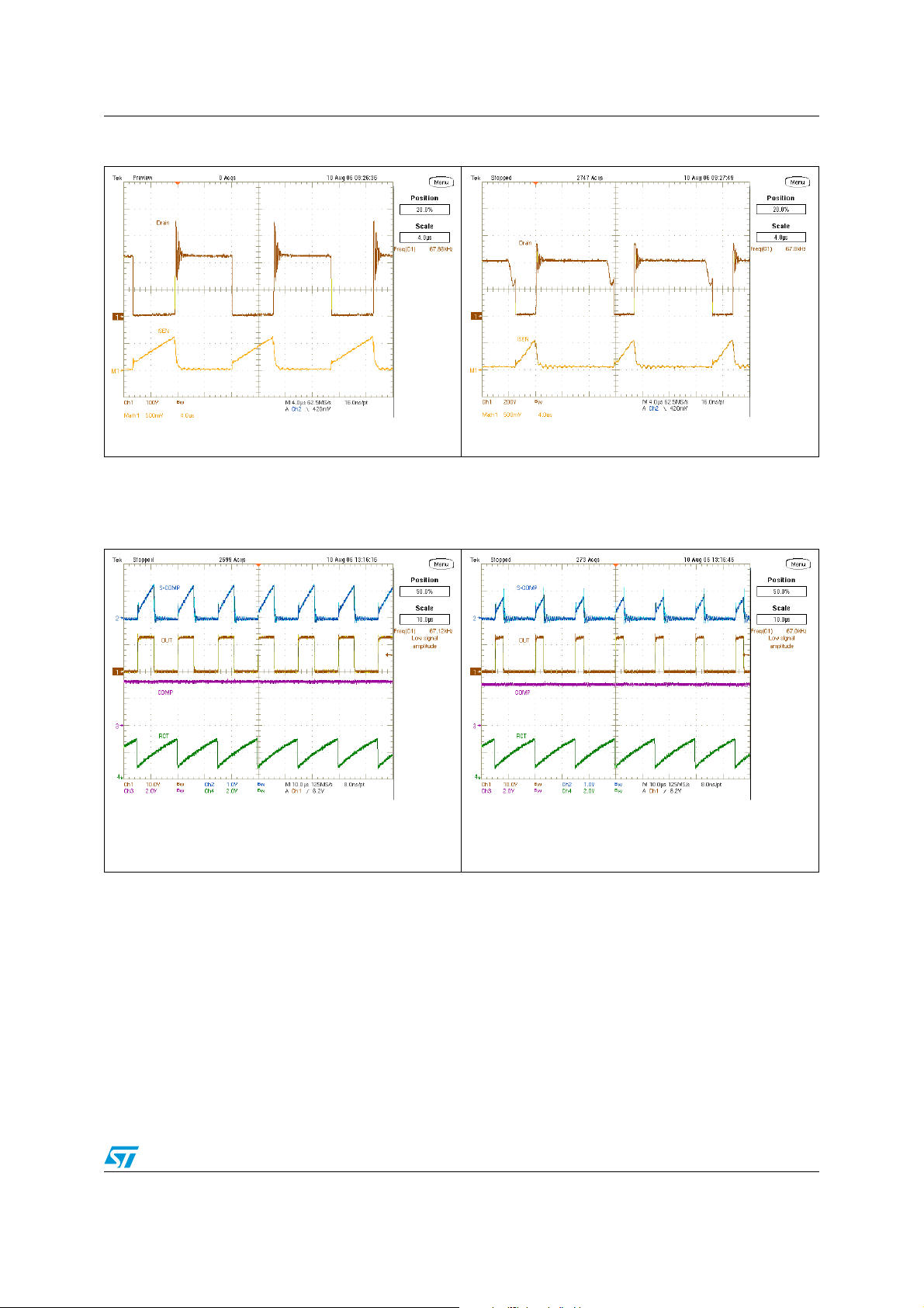
AN2432 Adapter features
Figure 2. V
IN
= 115V
- 60Hz Figure 3. VIN = 230V
RMS
Ch1: Q3 drain voltage
M1: ISEN pin voltage
Figure 4 and Figure 5 show some of most important signals of the L6668 while operating at
full load. The oscillator signal is stable and clean in all conditions.
Figure 4. VIN = 115V
- 60Hz Figure 5. VIN = 230V
RMS
Ch1: Q3 drain voltage
M1: ISEN pin voltage
RMS
RMS
- 50Hz
- 50Hz
CH1: Out
CH2: S-COMP
CH3: COMP
CH4: RCT
CH1: Out
CH2: S-COMP
CH3: COMP
CH4: RCT
On the secondary side, in CCM operation (full load with VIN = 115VAC), the gate drive of the
STSR30 is synchronized with the CK pin (copy of SR MOSFET drain voltage clamped at 5V)
as shown in Figure 6.
In Figure 7, the turn-off detail is zoomed and it is possible to see the anticipation amount
(225ns) and the jitter due to the digital counter inside the IC. In fact, most times the
anticipation has its typical value but sometimes the counter vary its value of ±1 cycle
(approximately ±70ns using the 14-MHz internal oscillator). In any case, cross-conduction is
always avoided.
8/27
Page 9
Adapter features AN2432
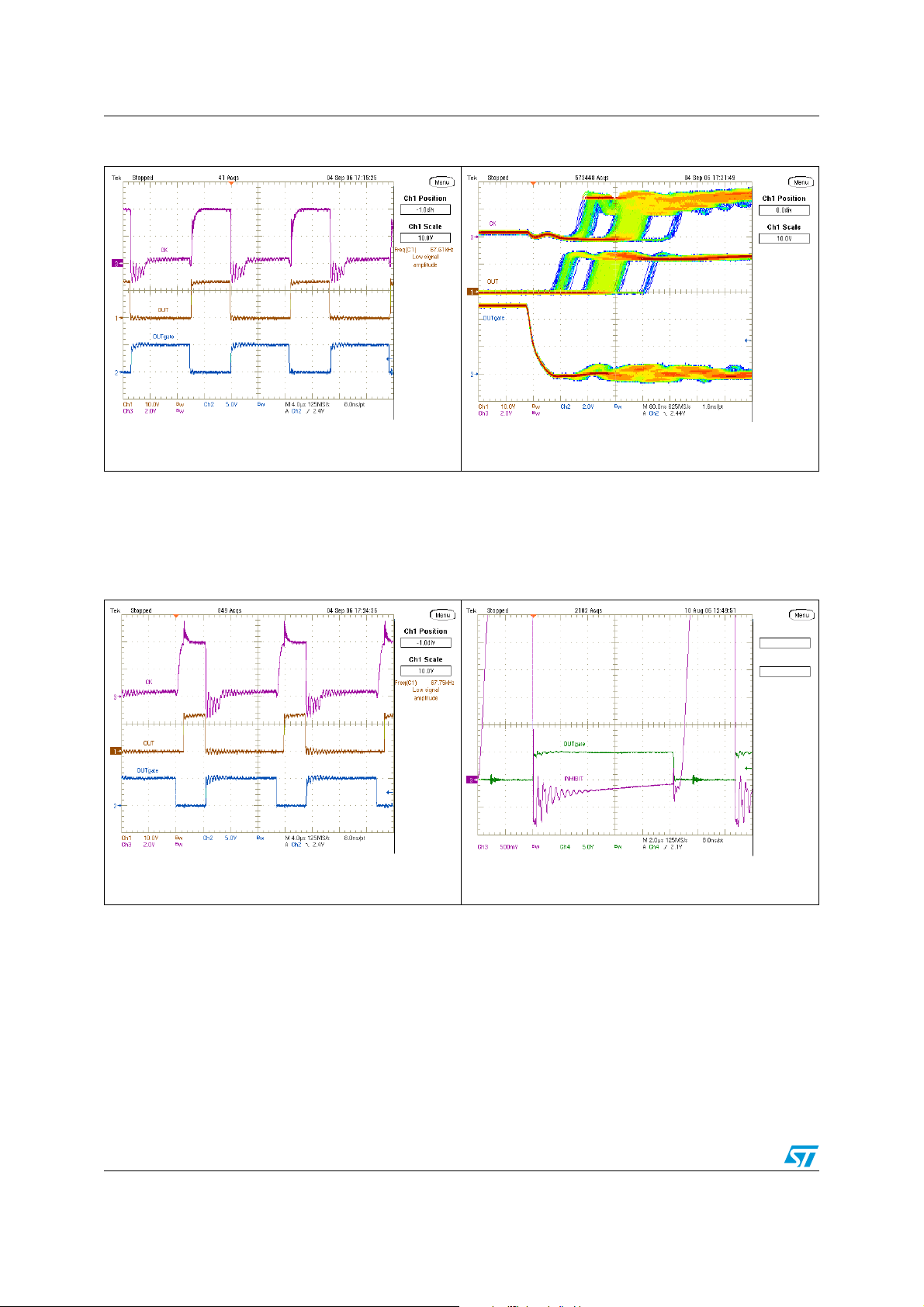
Figure 6. VIN = 115VAC - CCM Figure 7. CCM - Anticipation detail
CH1: L6668 gate drive
CH2: STSR30 gate drive
CH3: STSR30 CK pin
CH1: L6668 gate drive
CH2: STSR30 gate drive
CH3: STSR30 CK pin
In DCM operation, the gate-drive turn-on is still triggered by the falling edge of the CK pin
voltage, while turn-off is determined by the INHIBIT pin voltage crossing the -25mV internal
threshold. Figure 8 and Figure 9 show this mechanism at full load and V
= 230VAC
IN
conditions.
Figure 8. VIN = 230VAC - DCM Figure 9. DCM - INHIBIT synchronization
CH1: L6668 gate drive
CH2: STSR30 gate drive
CH3: STSR30 CK pin
9/27
CH3: STSR30 CK pin
CH4: STSR30 gate drive
Page 10

AN2432 Electrical performance
2 Electrical performance
Ta bl e 1 shows the output voltage values at different input voltage and load amount
conditions. Thanks to the good regulation, the maximum deviation is only about 10mV.
Table 1. Line and load regulation
V
[V] Input voltage [V
OUT
88 115 230 264
0 11.97 11.97 11.97 11.97
RMS
]
Output load [A]
1 11.97 11.97 11.97 11.98
3 11.98 11.98 11.98 11.98
5 11.98 11.98 11.98 11.98
In the next tables there are efficiency measurements taken at the two nominal voltages.
Table 2. Efficiency at 115V
Load [A] PIN [W] IIN [A] P
1.00 13.82 0.247 11.96 86.54
1.25 17.25 0.299 14.96 86.72
2.00 27.3 0.453 23.95 87.73
2.50 34.04 0.553 29.94 87.96
3.00 40.77 0.650 35.99 88.28
3.75 51.57 0.801 44.81 86.89
4.00 55.08 0.851 47.89 86.95
5.00 69.27 1.043 59.88 86.44
Table 3. Efficiency at 230V
Load [A] PIN [W] IIN [A] P
1.00 13.95 0.156 11.95 85.66
RMS
RMS
[W] Eff [%]
OUT
[W] Eff [%]
OUT
1.25 17.41 0.188 14.95 85.87
2.00 27.60 0.283 23.94 86.74
2.50 34.35 0.342 29.93 87.13
3.00 40.45 0.398 35.99 88.97
3.75 50.18 0.479 44.81 89.30
4.00 54.03 0.515 47.89 88.63
5.00 67.05 0.625 59.93 89.38
10/27
Page 11

Electrical performance AN2432
Ta bl e 4 shows the no-load consumption. The adapter has very good values (less than
200mW @ 230V
) thanks to the Burst mode operation and the high voltage startup of the
AC
L6668 and to the Disable mode of the STSR30.
Table 4. No load consumption
Value 88V
AC
115V
AC
230V
AC
264V
Pin [W] 0.126 0.133 0.178 0.205
Vcc [V] 9.70 9.72 9.75 9.74
In Figure 10, the most important waveform are taken during Burst mode with no load.
Figure 10. Burst mode operation at 230V
and no load
AC
AC
CH1: Q3 drain voltage
CH2: COMP pin voltage
CH3: RCT pin voltage
CH4: SKIPADJ pin voltage
For the same reasons as in no load condition, the adapter has good consumption values
also with 0.5W output power as shown in Ta bl e 5 for different input voltage values.
Table 5. Power consumption with 0.5W output
Val ue 88 V
AC
Pin [W] 0.735 0.747 0.830 0.880
It is interesting to compare the demo board results with the targets set by the most important
international energy saving programs. The results are shown in Ta bl e 6 (mandatory
requirements) and Tab le 7 (voluntary requirements). Both tables take into account the worst
nominal input voltage condition when measuring the no load consumption and efficiency
values. This application is already compliant with all future (from 1 January 2008) energy
programs.
11/27
115V
AC
230V
AC
264V
AC
Page 12

AN2432 Electrical performance
Table 6. Mandatory energy saving requirements (from 1 January 2008)
Energy
program
California
Energy
Commission
(CEC)
Australian < 0.5 W > 85%
China < 0.75 W > 82%
Table 7. Voluntary energy saving requirements (from 1 January 2008)
Energy
program
Energy Star < 0.5 W
Pin no load Measure Efficiency Measure Compliant
(1)
< 0.5 W
0.178 W
(@230V
AC
> 85%
)
87%
(@115V
87%
(@115V
(1)
AC
AC
)
)
86.44%
(@115V
AC
)
Pin no load Measure Efficiency Measure Compliant
(1)
> 84%
87%
(@115VAC)
COC (Code Of
Conduct)
European
< 0.3 W > 84%
0.178 W
(@230VAC)
86.44%
(@115V
AC
)
Union
China < 0.75 W > 85%
1. Efficiency measured at 25%, 50%, 75% and 100% of rated load and then averaged
86.44%
(@115V
AC
)
Ye s
Ye s
Ye s
Ye s
Ye s
Ye s
Another important measurement is the efficiency improvement given by the synchronous
rectification with respect to a standard (diode rectification) flyback. The test was performed
using a STPS8H100 Schottky diode instead of the SR MOSFET. The results are shown in
Ta bl e 8 . In a load range from 20% to 100% of the rated load, the average efficiency rise is
3.52% at 115V
Table 8. Comparison between standard and SR flyback
Val ue VIN = 115V
Load [A] Eff
1 86.54% 83.30% +3.24% 85.66% 82.26% +3.40%
2 87.73% 83.98% +3.75% 86.74% 83.62% +3.12%
3 88.28% 84.05% +4.23% 88.97% 84.80% +4.17%
4 86.95% 83.65% +3.30% 88.63% 84.98% +3.65%
5 86.44% 83.34% +3.10% 89.38% 84.97% +4.41%
and 3.75% at 230VAC.
AC
SR
Eff
diode
Average var @ 115V
AC
RMS
Var Ef f
SR
+3.52% Average var @ 230V
VIN = 230V
Eff
diode
AC
RMS
Var
+3.75%
12/27
Page 13

Functional check AN2432
3 Functional check
3.1 Start-up behavior at full load
Figure 11 and Figure 12 show the start-up phase at full output load at minimum and
maximum mains voltages. The rising time is nearly constant over all input voltage range.
The output voltage reaches its regulated value without any overshoot.
The soft-start function is integrated in the L6668 controller and can be programmed by
changing the value of C10.
Figure 11. Start-up at 88V
- 60Hz Figure 12. Start-up at 264VAC - 50Hz
AC
CH2: SS pin
CH3: Output voltage
3.2 Wake-up time
The wake-up time is the time needed for the output voltage to reach its nominal value from
the moment the adapter is plugged-in. Thanks to the internal high voltage start-up current
generator of the L6668, the wake-up time of this demo board is quite fast (approx. 900ms)
and, above all, independent of the mains voltage value.
When the IC starts, the generator is turned off, saving power in every working condition.
CH2: SS pin
CH3: Output voltage
13/27
Page 14

AN2432 Functional check
Figure 13. Wake-up at 115VAC - 60Hz Figure 14. Wake-up at 230VAC - 50Hz
CH1: Q3 drain voltage
CH2: Output voltage
CH3: Self supply voltage
CH1: Q3 drain voltage
CH2: Output voltage
CH3: Self supply voltage
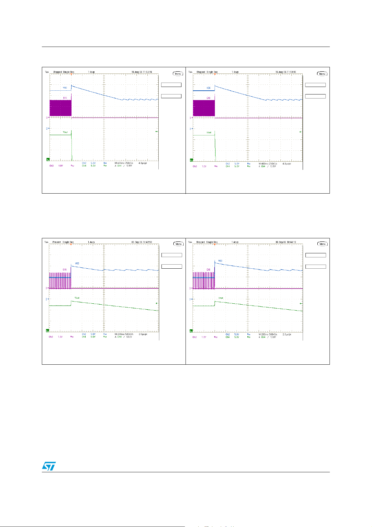
3.3 Power-down
Unplugging the adapter from the mains, the self supply and output voltages have clean
transition without restart trials or glitches. Figure 15 and Figure 16 show the power-down
waveforms at full load. It is possible to measure the hold-up time that, in the worst case
(115V
Figure 15. Power-down at 115VAC - 60Hz Figure 16. Power-down at 230VAC - 50Hz
), is approximately 16ms.
AC
CH1: Q3 drain voltage
CH2: Output voltage
CH3: Self supply voltage
CH1: Q3 drain voltage
CH2: Output voltage
CH3: Self supply voltage
14/27
Page 15

Functional check AN2432
3.4 Short-circuit tests
The demo board has been tested with a short circuit directly on the output connector. During
this fault condition, the circuit works in Hiccup mode thanks to the lack of self supply. Once
the short-circuit is removed, the converter restarts working normally. The high voltage startup generator of the L6668 ensures having constant on-off periods. The average output
current during the short-circuit is well below the nominal value (approx. 0.8A).
Figure 17. Short circuit at 88V
- 60Hz Figure 18. Short circuit at 264VAC - 50Hz
AC
CH1: Q3 drain voltage
CH2: Self supply voltage
CH4: Short circuit current
3.5 Overvoltage protection
The DIS pin of the L6668 is dedicated to a latched protection of the circuit. In this
application, it is used to provide overvoltage protection using components D11, R19, R28
and C13 connected to the auxiliary winding of the transformer. This network provides a
mean rectified value cycle by cycle of the auxiliary voltage that tracks the output voltage. In
the following figures, a feedback failure is simulated (open loop) and the most interesting
waveforms are shown. As explained, this protection is latched and it is necessary to recycle
the input power to restart the circuit.
Figure 19 and Figure 20 show the OVP protection intervention while the converter is
operating at full load. In the whole input range during fault condition, V
V
reaches 20V.
CC
CH1: Q3 drain voltage
CH2: Self supply voltage
CH3: Short circuit current
reaches 14V and
OUT
15/27
Page 16
AN2432 Functional check
Figure 19. OVP at 115VAC - full load Figure 20. OVP at 230VAC - full load
CH2: Self supply voltage
CH3: DIS pin voltage
CH4: Output voltage
CH2: Self supply voltage
CH3: DIS pin voltage
CH4: Output voltage
Also during no-load operations (Figure 21 and Figure 22), the OVP protection stops the
converter at similar V
voltage levels (14.2V). The VCC voltage value reaches lower
OUT
values (16.5V) in respect to full load condition since it starts from approximately 10V.
Figure 21. OVP at 115VAC - no load Figure 22. OVP at 230VAC - no load
CH2: Self supply voltage
CH3: DIS pin voltage
CH4: Output voltage
CH2: Self supply voltage
CH3: DIS pin voltage
CH4: Output voltage
16/27
Page 17
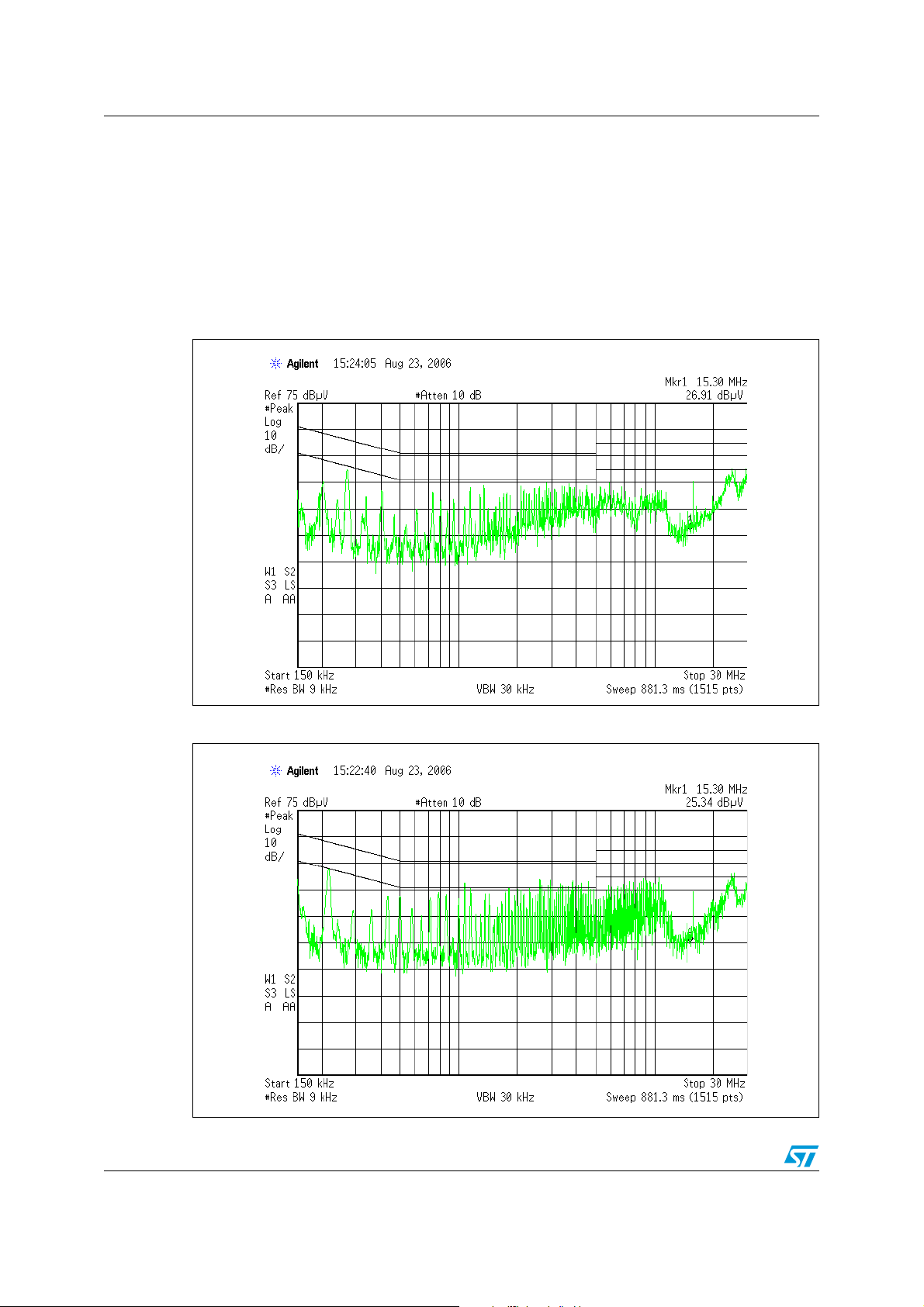
Conducted noise measurements (pre-compliance test) AN2432
4 Conducted noise measurements (pre-compliance
test)
The next two figures show the conducted noise measurements performed at the two
nominal voltages with peak detection and considering only the worst phase. The
measurements have a good margin with respect to the limits (stated in EN55022 Class-B
specifications).
Figure 23. CE peak measure at 115V
Figure 24. CE peak measure at 230V
and full load
AC
and full load
AC
17/27
Page 18

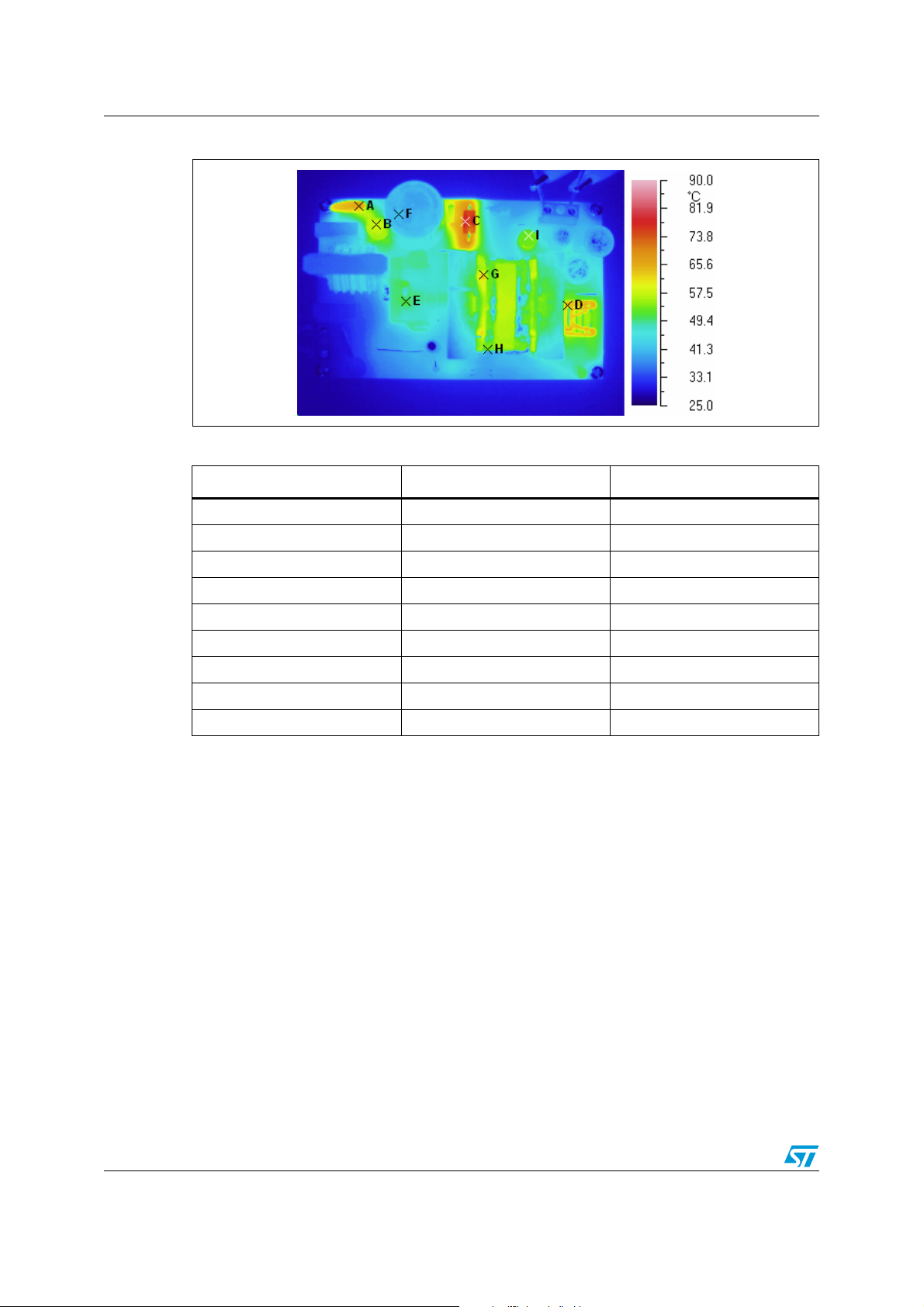
AN2432 Thermal measurements
5 Thermal measurements
A thermal analysis of the board was performed using an IR camera. The results are shown
in Figure 25 and Figure 26 for 115V
load condition.
–T
= 28°C for both figures
AMB
– Emissivity = 0.9 for all points
and 230VAC mains input. Both images refer to full
AC
Figure 25. V
Table 9. Key components temperature at 115VAC - full load
= 115VAC - full load
IN
Point Temp [°C] Ref
A88.2NTC1
B 81.6 D7 (bridge)
C 87.8 D8 (clamp)
D 80.3 Q1 (SR MOS)
E60.0Q3
F46.1C8
G 64.2 T1 (windings)
H 55.1 T1 (ferrite)
I54.7L2
18/27
Page 19
Thermal measurements AN2432
Figure 26. VIN = 230VAC - full load
Table 10. Key components temperature at 230VAC - full load
Point Temp [°C] Ref
A66.2NTC1
B 58.3 D7 (bridge)
C 80.0 D8 (clamp)
D 65.6 Q1 (SR MOS)
E51.8Q3
F41.6C8
G 63.4 T1 (windings)
H 54.4 T1 (ferrite)
I53.8L2
19/27
Page 20

AN2432 Bill of materials
6 Bill of materials
Ta bl e 1 1 lists the parts of the demo board.
Table 11. Part list
Ref Part Value Description Manufacturer
C1 1000uF - 25V Aluminium ELCAP 25ZL1000M12.5x20 - 105°C Rubycon
C2 100nF - 50V CERCAP X7R - General purpose AVX
C3 100nF - 50V CERCAP X7R - General purpose AVX
C4 4.7nF - 50V CERCAP X7R - General purpose AVX
C5 1nF - 250V Polyester CAP R82IC3100DQ02J Arcotronics
C6 47uF - 25V Aluminium ELCAP - YXF series - 105°C Rubycon
C7 470nF - 16V CERCAP X7R - General purpose AVX
C8 100uF - 400V
C9 1nF - 50V CERCAP X7R - General purpose AVX
C10 68nF - 50V CERCAP X7R - General purpose AVX
C11 1nF - 50V CERCAP NP0 - General purpose - 1% AVX
C12 100nF - 50V CERCAP X7R - General purpose AVX
C13 470pF - 50V CERCAP NP0 - General purpose AVX
C14 100nF - 275Vac X2 film CAP - R46KI 3100xx M1 M Arcotronics
C15 100nF - 275Vac X2 film CAP - R46KI 3100xx M1 M Arcotronics
C16 100nF - 50V CERCAP X7R - General purpose AVX
C17 2.2nF - 50V CERCAP X7R - General purpose AVX
C18 2.2nF - 250Vac Y1 safety CAP - DE1E3KX222M Murata
C19 1000uF - 25V Aluminium ELCAP 25ZL1000M12.5x20 - 105°C Rubycon
C20 220pF - 50V CERCAP NP0 - General purpose AVX
C21 100uF - 35V Aluminium ELCAP - YXF series - 105°C Rubycon
C22 470nF - 16V CERCAP X7R - General purpose AVX
C23 220pF - 50V CERCAP NP0 - General purpose AVX
C24 220pF - 50V CERCAP NP0 - General purpose AVX
Aluminium ELCAP TS-UP series - ECEC2GP101BB 85°C
Panasonic
C25 100nF -50V CERCAP X7R - General purpose AVX
C26 N.M. CERCAP X7R - General purpose ---
C27 100pF -50V CERCAP NP0 - General purpose AVX
C28 1nF - 50V CERCAP X7R - General purpose AVX
C29 100nF - 50V CERCAP X7R - General purpose AVX
D1 STPS2H100 Power Schottky rectifier STMicroelectronics
20/27
Page 21

Bill of materials AN2432
Table 11. Part list (continued)
Ref Part Value Description Manufacturer
D2 LL4148 Fast switching diode Vishay
D3 LL4148 Fast switching diode Vishay
D4 LL4148 Fast switching diode Vishay
D5 STTH1L06U Ultrafast high voltage rectifier STMicroelectronics
D6 BAV103 Fast switching diode Vishay
D7 W06G Single phase bridge rectifier Vishay
D8 1.5KE200A Transil STMicroelectronics
D9 1N4148WS Fast switching diode Vishay
D10 LL4148 Fast switching diode Vishay
D11 BAV103 Fast switching diode Vishay
F1 T2A PCB FUSE 2A time delay TR5 - 372 1200 Wickmann
J1 MKDS 1,5/3-5.08 PCB term. block, screw conn., pitch 5.08 Phoenix Contact
J2 MKDS 1,5/3-5.08 PCB term. block, screw conn., pitch 5.08 Phoenix Contact
L1 2x27mH Common mode choke coil - B82734-R2172-B30 EPCOS
L2 2u2 Power inductor - RFB0807-2R2L Coilcraft
L3 100uH RF inductor - B78108S1104J000 EPCOS
NTC1 5R - S237 NTC resistor - B57237S0509M000 EPCOS
Q1 STP75NF75L N-channel Power MOSFET STMicroelectronics
Q1 FK 242 SA 220 O Heatsink Fischer
Q2 BC807-25 Small signal PNP transistor Vishay
Q3 STP9NK70ZFP N-channel Power MOSFET STMicroelectronics
Q3 593002B03400 Heatsink Aavid
RV1 S14K275 Varistor - B72214S0271K101 EPCOS
R1 1k SMD standard film resistor - 0805 - 5% - 250ppm/°C Vishay
R2 1k SMD standard film resistor - 0805 - 5% - 250ppm/°C Vishay
R3 22 SMD standard film resistor - 0805 - 5% - 250ppm/°C Vishay
R4 33k SMD standard film resistor - 1206 - 5% - 250ppm/°C Vishay
R5 33k SMD standard film resistor - 0805 - 5% - 250ppm/°C Vishay
R6 100k SMD standard film resistor - 0805 - 1% - 100ppm/°C Vishay
R8 33k SMD standard film resistor - 0805 - 5% - 250ppm/°C Vishay
R9 0.56 SMD standard film resistor - 1206 - 1% - 100ppm/°C Vishay
R10 0.56 SMD standard film resistor - 1206 - 1% - 100ppm/°C Vishay
R11 22 SMD standard film resistor - 0805 - 5% - 250ppm/°C Vishay
R12 1k SMD standard film resistor - 0805 - 5% - 250ppm/°C Vishay
R13 N.M. SMD standard film resistor - 0805 Vishay
21/27
Page 22

AN2432 Bill of materials
Table 11. Part list (continued)
Ref Part Value Description Manufacturer
R14 2.2k SMD standard film resistor - 0805 - 1% - 100ppm/°C Vishay
R15 68k SMD standard film resistor - 1206 - 1% - 100ppm/°C Vishay
R16 2.7Meg SMD standard film resistor - 1206 - 1% - 100ppm/°C Vishay
R17 2.7Meg SMD standard film resistor - 1206 - 1% - 100ppm/°C Vishay
R18 9.1k SMD standard film resistor - 0805 - 1% - 100ppm/°C Vishay
R19 33k SMD standard film resistor - 0805 - 1% - 100ppm/°C Vishay
R20 2.7k SMD standard film resistor - 0805 - 5% - 250ppm/°C Vishay
R21 20k SMD standard film resistor - 0805 - 1% - 100ppm/°C Vishay
R22 1.5k SMD standard film resistor - 0805 - 1% - 100ppm/°C Vishay
R23 N.M. SMD standard film resistor - 0805 Vishay
R24 47k SMD standard film resistor- 1206 - 1% - 100ppm/°C Vishay
R25 15k SMD standard film resistor - 1206 - 1% - 100ppm/°C Vishay
R27 20k SMD standard film resistor - 0805 - 1% - 100ppm/°C Vishay
R26 82k SMD standard film resistor - 0805 - 1% - 100ppm/°C Vishay
R28 3.9k SMD standard film resistor - 0805 - 1% - 100ppm/°C Vishay
R29 10 SMD standard film resistor - 0805 - 5% - 250ppm/°C Vishay
R32 0 SMD standard film resistor - 0805 Vishay
R33 9.1k SMD standard film resistor - 0805 - 1% - 100ppm/°C Vishay
R34 0 SMD standard film resistor - 1206 Vishay
R37 330k SMD standard film resistor - 0805 - 1% - 100ppm/°C Vishay
R38 33k SMD standard film resistor - 1206 - 5% - 250ppm/°C Vishay
R39 0 SMD standard film resistor - 1206 Vishay
R40 1Meg SMD standard film resistor - 1206 - 1% - 100ppm/°C Vishay
T1 See Spec Power transformer
U1 STSR30D Synchronous rectifier smart driver STMicroelectronics
U2 L78L05ACZ Voltage regulator STMicroelectronics
U3 L6668 Smart primary controller STMicroelectronics
U4 TSM1015ID Voltage and current controller STMicroelectronics
U5 PC817X2J000F Optocoupler Sharp
22/27
Page 23
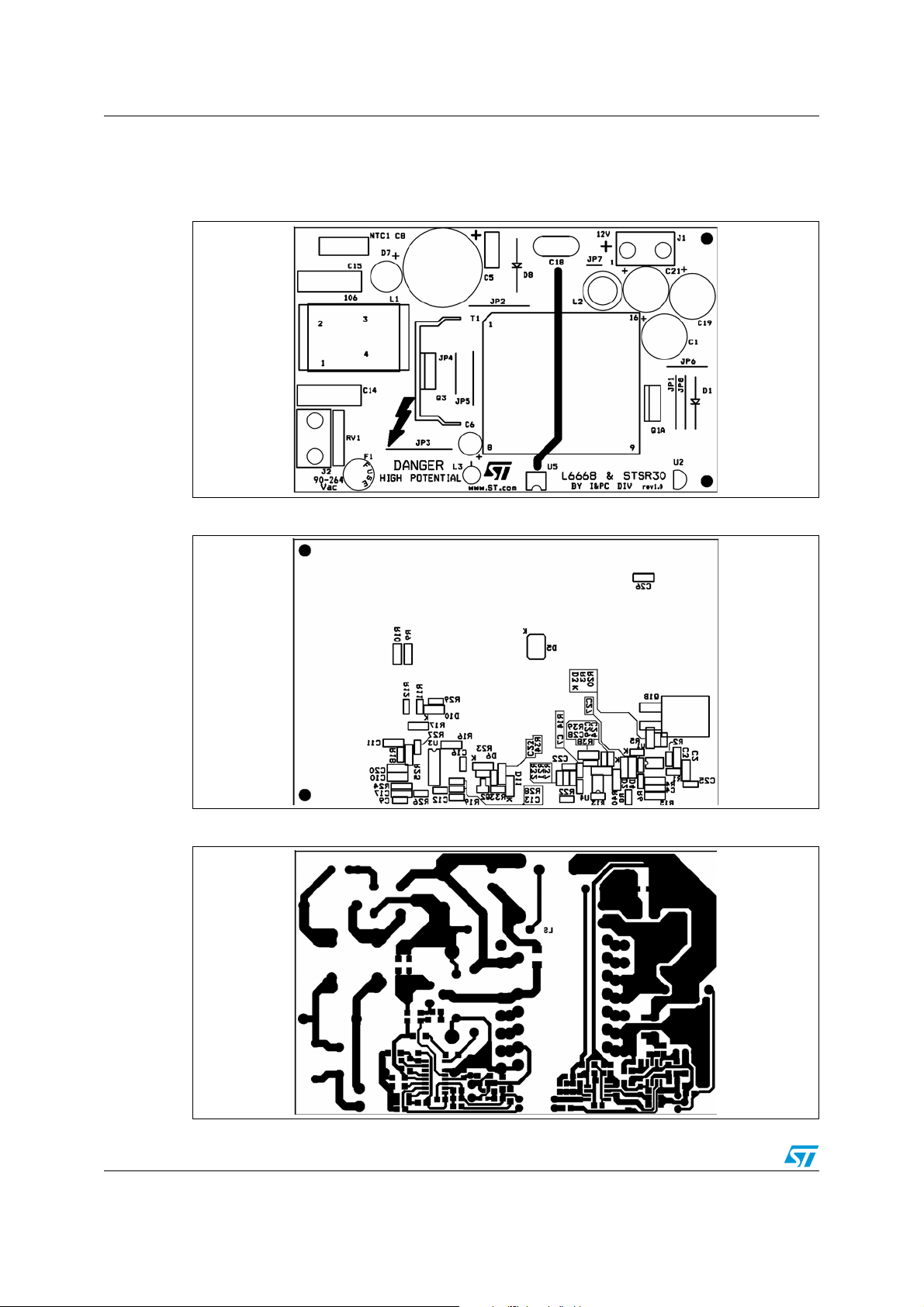
PCB layout AN2432
7 PCB layout
Figure 27. Silk screen - top side
Figure 28. Silk screen - bottom side
Figure 29. Copper tracks
23/27
Page 24
AN2432 Transformer specification
8 Transformer specification
● Application type: Consumer, Home Appliance
● Transformer type: Open
● Winding type: Layer
● Coil former: Horizontal type, 7+7 pins
● Maximum temperature increase: 45° C
● Maximum operating ambient temperature: 60° C
● Mains insulation: according with EN60065
8.1 Electrical characteristics
● Converter topology: Flyback, CCM/DCM mode
● Core type: ETD34 - N87 or equivalent
● Typical operating frequency: 70 kHz
● Primary inductance: 530 µH ±10% @1 kHz - 0.25V (Note 1)
● Air Gap: 1.2mm on central leg (std. value)
● Leakage inductance: 9 µH (Maximum) @ 100 kHz - 0.25V (Note 2)
● Maximum peak primary current: 3.7 A
●
RMS primary current: 1.06 A
Note: 1 Measured between pins 1 and 3
2 Measured between pins 1 and 3 with secondary shorted
RMS
pk
Figure 30. Transformer electrical diagram
1
PRIM.
3
6
AUX
7
13
12
SEC.
10
9
24/27
Page 25
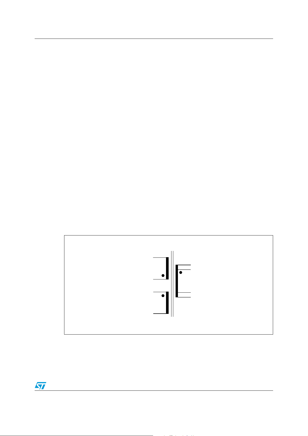
Transformer specification AN2432
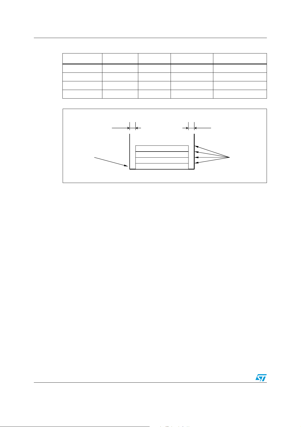
Table 12. Winding characteristics
Pins Winding RMS current Number of turns Wire type
3 – 2 PRIMARY - A 1.06 A
12, 13 – 9, 10 SECONDARY 7.4 A
2 – 1 PRIMARY - B 1.06 A
6 – 7 AUX 0.05 A
RMS
RMS
RMS
RMS
12 Spaced G2 – φ 0.25 mm
Figure 31. Windings position
3mm 3mm
AUX
coil former
COIL FORMER
PRIMARY - B
SECONDARY
PRIMARY - A
Note: Primaries A and B are in series.
Note: Cover primary and auxiliary wire ends with silicon sleeve.
32 G2 – 2 x φ 0.45 mm
8 G2 – 60 x φ 0.18 mm
31 G2– 2 x φ 0.45 mm
insulating
INSULATING
tape
TAPE
8.2 Mechanical aspect
● Maximum height from PCB: 35 mm
● Coil former type: horizontal, 7+7 pins (Pins #2 and #8 removed)
● Pins pitch: 5.08 mm
● Rows distance: 25.4 mm
● Pins #2 and #8 removed
● External copper shield: 12 mm width
25/27
Page 26

AN2432 Revision history
9 Revision history
Table 13. Revision history
Date Revision Changes
26-Sept-2006 1 Initial release
23-Oct-2006 2 Minor text changes
26/27
Page 27

AN2432
Please Read Carefully:
Information in this document is provided solely in connection with ST products. STMicroelectronics NV and its subsidiaries (“ST”) reserve the
right to make changes, corrections, modifications or improvements, to this document, and the products and services described herein at any
time, without notice.
All ST products are sold pursuant to ST’s terms and conditions of sale.
Purchasers are solely responsible for the choice, selection and use of the ST products and services described herein, and ST assumes no
liability whatsoever relating to the choice, selection or use of the ST products and services described herein.
No license, express or implied, by estoppel or otherwise, to any intellectual property rights is granted under this document. If any part of this
document refers to any third party products or services it shall not be deemed a license grant by ST for the use of such third party products
or services, or any intellectual property contained therein or considered as a warranty covering the use in any manner whatsoever of such
third party products or services or any intellectual property contained therein.
UNLESS OTHERWISE SET FORTH IN ST’S TERMS AND CONDITIONS OF SALE ST DISCLAIMS ANY EXPRESS OR IMPLIED
WARRANTY WITH RESPECT TO THE USE AND/OR SALE OF ST PRODUCTS INCLUDING WITHOUT LIMITATION IMPLIED
WARRANTIES OF MERCHANTABILITY, FITNESS FOR A PARTICULAR PURPOSE (AND THEIR EQUIVALENTS UNDER THE LAWS
OF ANY JURISDICTION), OR INFRINGEMENT OF ANY PATENT, COPYRIGHT OR OTHER INTELLECTUAL PROPERTY RIGHT.
UNLESS EXPRESSLY APPROVED IN WRITING BY AN AUTHORIZED ST REPRESENTATIVE, ST PRODUCTS ARE NOT
RECOMMENDED, AUTHORIZED OR WARRANTED FOR USE IN MILITARY, AIR CRAFT, SPACE, LIFE SAVING, OR LIFE SUSTAINING
APPLICATIONS, NOR IN PRODUCTS OR SYSTEMS WHERE FAILURE OR MALFUNCTION MAY RESULT IN PERSONAL INJURY,
DEATH, OR SEVERE PROPERTY OR ENVIRONMENTAL DAMAGE. ST PRODUCTS WHICH ARE NOT SPECIFIED AS "AUTOMOTIVE
GRADE" MAY ONLY BE USED IN AUTOMOTIVE APPLICATIONS AT USER’S OWN RISK.
Resale of ST products with provisions different from the statements and/or technical features set forth in this document shall immediately void
any warranty granted by ST for the ST product or service described herein and shall not create or extend in any manner whatsoever, any
liability of ST.
ST and the ST logo are trademarks or registered trademarks of ST in various countries.
Information in this document supersedes and replaces all information previously supplied.
The ST logo is a registered trademark of STMicroelectronics. All other names are the property of their respective owners.
© 2006 STMicroelectronics - All rights reserved
STMicroelectronics group of companies
Australia - Belgium - Brazil - Canada - China - Czech Republic - Finland - France - Germany - Hong Kong - India - Israel - Italy - Japan -
Malaysia - Malta - Morocco - Singapore - Spain - Sweden - Switzerland - United Kingdom - United States of America
www.st.com
27/27
 Loading...