

Page 1

AN2430
Application note
STR75x SystemMemory boot mode
Introduction
This application note describes the features of the SystemMemory boot mode developed for
STR75x Flash microcontrollers providing all the basic functionality to support the
programming of the embedded Flash. As well as the general features, this document also
covers the specific features of the UART boot mode.
Note: The bootloader feature is unavailable on some devices soldered on development tools
(starter kits or evaluation boards). Please refer to Section 4 on page 22 for further
information.
January 2007 Rev 3 1/24
www.st.com
Page 2

Contents AN2430
Contents
1 General description . . . . . . . . . . . . . . . . . . . . . . . . . . . . . . . . . . . . . . . . . . 3
1.1 Entering SystemMemory boot mode . . . . . . . . . . . . . . . . . . . . . . . . . . . . . 3
1.2 Hardware requirements . . . . . . . . . . . . . . . . . . . . . . . . . . . . . . . . . . . . . . . 3
1.3 Using SystemMemory boot mode . . . . . . . . . . . . . . . . . . . . . . . . . . . . . . . 4
1.4 Command description . . . . . . . . . . . . . . . . . . . . . . . . . . . . . . . . . . . . . . . . 5
1.4.1 Get command . . . . . . . . . . . . . . . . . . . . . . . . . . . . . . . . . . . . . . . . . . . . . 5
1.4.2 Read Memory command . . . . . . . . . . . . . . . . . . . . . . . . . . . . . . . . . . . . . 6
1.4.3 Go command . . . . . . . . . . . . . . . . . . . . . . . . . . . . . . . . . . . . . . . . . . . . . . 7
1.4.4 Write Memory command . . . . . . . . . . . . . . . . . . . . . . . . . . . . . . . . . . . . . 8
1.4.5 Erase command . . . . . . . . . . . . . . . . . . . . . . . . . . . . . . . . . . . . . . . . . . . 10
1.4.6 Write Protection command . . . . . . . . . . . . . . . . . . . . . . . . . . . . . . . . . . 12
1.4.7 Write Unprotection command . . . . . . . . . . . . . . . . . . . . . . . . . . . . . . . . 13
1.4.8 Readout Permanent Protect command . . . . . . . . . . . . . . . . . . . . . . . . . 14
1.4.9 Readout Temporary Unprotect command . . . . . . . . . . . . . . . . . . . . . . . 15
1.4.10 Readout Permanent Unprotect command . . . . . . . . . . . . . . . . . . . . . . . 16
1.5 Exiting SystemMemory boot mode . . . . . . . . . . . . . . . . . . . . . . . . . . . . . 17
1.6 SystemMemory code program flow . . . . . . . . . . . . . . . . . . . . . . . . . . . . . 17
2 UART SystemMemory boot mode . . . . . . . . . . . . . . . . . . . . . . . . . . . . . 19
2.1 UART SystemMemory code sequence . . . . . . . . . . . . . . . . . . . . . . . . . . 19
2.2 Choosing the UART baud rate . . . . . . . . . . . . . . . . . . . . . . . . . . . . . . . . . 19
2.2.1 Minimum baud rate . . . . . . . . . . . . . . . . . . . . . . . . . . . . . . . . . . . . . . . . 19
2.2.2 The maximum baud rate . . . . . . . . . . . . . . . . . . . . . . . . . . . . . . . . . . . . 20
2.2.3 Higher baud rate deviations . . . . . . . . . . . . . . . . . . . . . . . . . . . . . . . . . . 20
3 Conclusion . . . . . . . . . . . . . . . . . . . . . . . . . . . . . . . . . . . . . . . . . . . . . . . . 21
4 Bootloader availability limitations . . . . . . . . . . . . . . . . . . . . . . . . . . . . . 22
5 Revision history . . . . . . . . . . . . . . . . . . . . . . . . . . . . . . . . . . . . . . . . . . . 23
2/24
Page 3

AN2430 General description
1 General description
The STR75x is usually woken up in SystemMemory boot Mode when the Flash is still not
programmed in the manufacturing line environment. In this case the system boot is
performed from SystemMemory sector in the Flash bank0. This mode allows initialization of
the Flash programming via a serial interface and the use of the Internal Free Running
Oscillator.
1.1 Entering SystemMemory boot mode
The STR75x enters the SystemMemory Boot Mode if the BOOT pins are configured as
follows:
● BOOT0 = 1
● BOOT1= 0
The value of the BOOT pin is latched on the 4th rising edge of CK_SYS after Reset.
After Reset, the STR75x CPU begins execution of the SystemMemory code which resides
in the SystemMemory sector.
Table 1. STR75x device configuration in SystemMemory Boot Mode
Feature/Peripheral State Comment
Instruction Set THUMB Save code space with 16-bit instructions
CPU Mode Supervisor Full access with IRQ Enabled and FIQs disabled
Input Clock
UART0_RX Pin Input UART0 Receive
UART0_TX Pin Output UART0 Transmit
UART0 Registers Default Only configured for UART Boot
Internal
FREEOSC
1.2 Hardware requirements
The hardware required to put the STR75x into SystemMemory boot mode consists of any
circuitry, switch, or jumper capable of holding the BOOT0 pin high and the BOOT1 pin low
during Reset.
To connect to the STR75x during SystemMemory boot mode, a RS232 serial interface must
be directly linked to UART0 pins.
For more details, refer to the STR75x hardware development getting started application note
(AN2419).
Allow a Frequency in a range of 2 to 10MHz
3/24
Page 4

General description AN2430
1.3 Using SystemMemory boot mode
The SystemMemory boot mode is executed from RAM and uses the last 4K of 16K RAM,
i.e. from 0x40003000 to 0x40003FFF. So when downloading code to RAM, the user has to
consider only the 12K RAM (from 0x40000000 to 0x40002FFF).
After the serial link initialization sequence (see the following chapters) the SystemMemory
code waits for the user to run some commands.
The supported commands are listed in the table below.
Table 2. Allowed commands
Command
Command
Code
Command Description
Get 0x01
Read Memory 0x11
Go 0x21
Write Memory 0x31
Erase 0x43 Erase from one to all the Flash sectors
Write Protection 0x63
Write Unprotection 0x71 Temporarily disable the write protection for all Flash sectors
Readout Permanent
Protect
Readout Temporary
Unprotect
Readout Permanent
Unprotect
0x82 Permanently enable the the Readout protection
0x91 Temporarily disable the Readout protection
0x92 Permanently disable the Readout protection
Get the SystemMemory version and the number of times
the readout protection is disabled/enabled.
Read until 256 bytes of memory starting from an address
specified by the user
Jump to an address specified by the user to execute a
loaded code
Write until 256 bytes to the RAM or the Flash starting from
an address specified by the user
Permanently enable the write protection for the needed
sectors
4/24
Page 5

AN2430 General description
1.4 Command description
1.4.1 Get command
Description:
This command allows the user to get the version of the bootloader, the number of times the
Readout protection is both disabled and enabled.
When the bootloader receives the Get command, it transmits four bytes to the user: the first
byte contains the version, the second contains the number of times the Readout protection
is disabled, the third contains the number of times it’s enabled and finally the ACK byte.
Figure 1. Get command flowchart
Start GC
Received byte
== 0x01?
Send the version of the bootloader
Send the number of times the Readout
protection is Disabled
Send the number of times the Readout
protection is enabled
Send ACK byte
End of GC
No
Send NACK byte
5/24
Page 6

General description AN2430
1.4.2 Read Memory command
Description:
This command allows the user to read the memory (RAM, Flash and registers).
When the bootloader receives the Read Memory command, it transmits the ACK byte.
After the transmission of the ACK byte, the bootloader waits for an address (4 bytes, byte 1
is the MSB and byte 4 is LSB of the address), checks this address, if the address is valid, it
transmits an ACK byte otherwise it transmits a NACK byte (0x3F) and exits from the
command.
When the address is valid, the bootloader waits for the number of bytes to be transmitted (N
bytes) and then returns to the user the needed data ((N + 1) bytes) starting from the
received address.
Figure 2. Read memory flowchart
Start RM
Received byte
== 0x11?
Send ACK byte
Receive the start address (4 bytes)
Valid Address?
Send ACK byte
Receive the number of bytes to be read
(1 byte)
Send data to the user
End of RM
No
No
Send NACK byte
6/24
Page 7

AN2430 General description
1.4.3 Go command
Description:
This command allows the user to execute the downloaded code or any other code by
making a branch to an address specified by the user.
When the bootloader receives the GO command, it transmits the ACK byte.
After the transmission of the ACK byte, the bootloader waits for an address (4 bytes, byte 1
is the MSB and byte 4 is LSB of the address), checks this address, if the address is valid, it
transmits an ACK byte otherwise it returns a NACK byte (0x3F) and exits from the
command.
When the address is valid, the program counter of the CPU jumps automatically to this
address. Therefore, the SystemMemory boot mode is exited.
Note: During SystemMemory mode, the CPU is in Thumb state.
Figure 3. Go command flowchart
Start GO
Received byte
== 0x21?
Send ACK byte
Receive the start address (4 bytes)
Valid Address?
Send ACK byte
Jump to start address
Exit SystemMemory
boot mode
No
No
Send NACK byte
End of GO
7/24
Page 8

General description AN2430
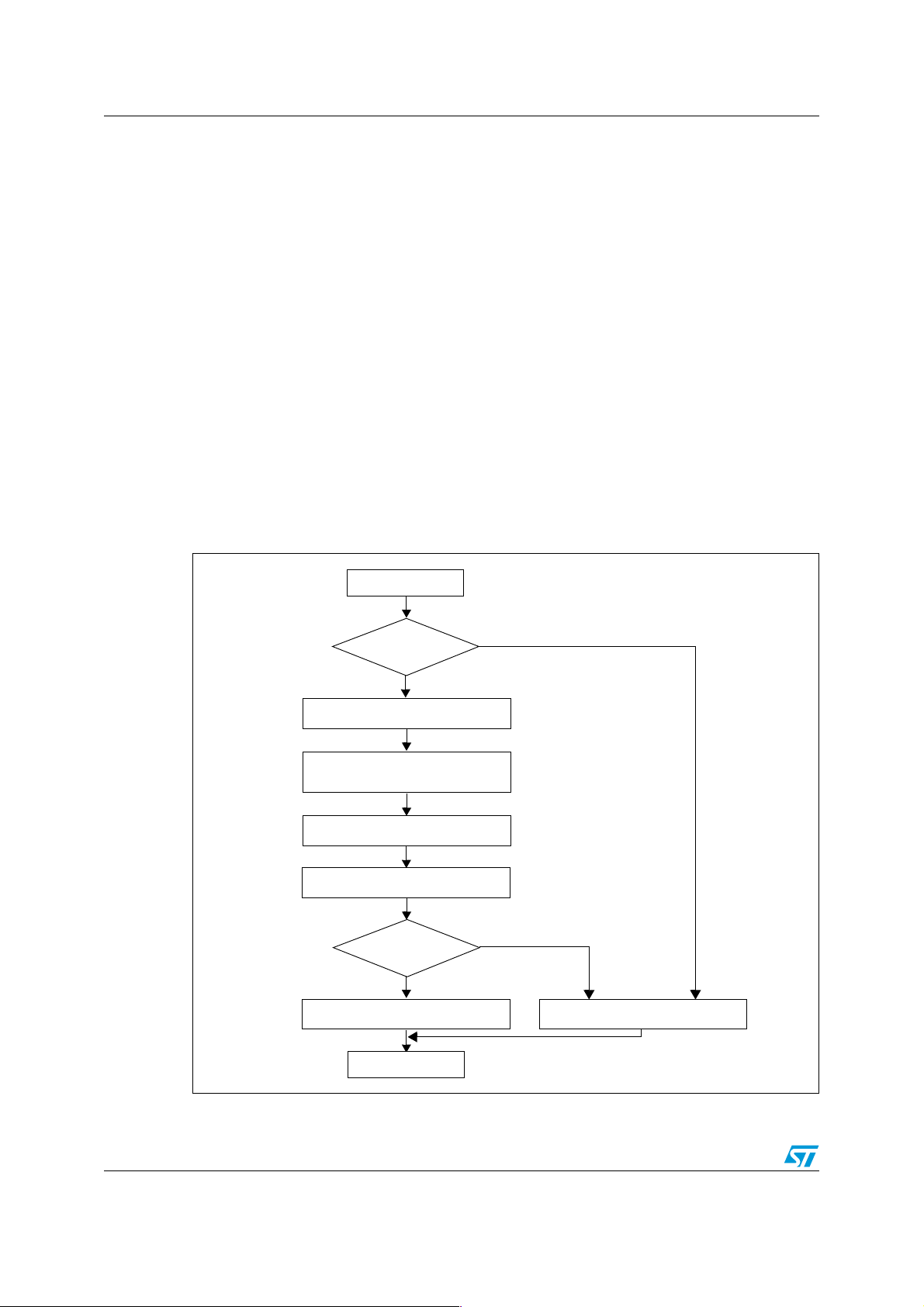
1.4.4 Write Memory command
Description:
This command allows the user to write data to any address memory (RAM, Flash or
registers).
When the bootloader receives the Write Memory command, it transmits to the user the ACK
byte.
After the transmission of the ACK byte, the bootloader waits for an address (4 bytes, byte 1
is the MSB and byte 4 is LSB of the address), checks this address, if the address is valid, it
transmits an ACK byte otherwise it returns a NACK byte (0x3F) and exits from the
command.
When the address is valid, the bootloader:
● Gets a byte which describes the amount of data to be received (N bytes),
● Receives the user data ((N + 1) bytes),
● Programs the user data to memory starting from the received address,
Finally, at the end of the command, the bootloader transmits the ACK byte if the write
operation is completed successfully otherwise a NACK byte (0x3F) is returned and the
command is exited.
8/24
Page 9

AN2430 General description
Figure 4. Write memory command flowchart
Start WM
Received byte
== 0x31?
Send ACK byte
Receive the start address (4 bytes)
Valid Address?
Send ACK byte
Receive the number of bytes to be written
(1 byte)
RAM Address?
No
No
No
Write the received data to RAM
from the start address
Send ACK byte
End of WM
Write the received data to Flash
from the start address
Write error?
No
Send NACK byte
9/24
Page 10

General description AN2430
1.4.5 Erase command
Description:
This command allows the user to erase from one to all the sectors of the Flash memory.
When the bootloader receives the Sector Erase command, it transmits the ACK byte.
After the transmission of the ACK byte, the bootloader waits for the number of bytes to be
received (number of sectors to be erased) and then receives from the user the Flash sectors
codes.
Finally, at the end of the command, the bootloader transmits the ACK byte if the erase is
completed successfully otherwise a NACK byte (0x3F) is returned and the command is
exited.
The Erase command procedure is as follows:
1. Receive one byte which contains the number (N) of sectors to be erased.Here, N can
be a value from 0 to 9,
2. Receive (N + 1) bytes, each byte contains a sector code. Below all the STR75x sector
codes.
Table 3. Sector codes
Flash Sector Sector Code
Bank 0 Sector 0 0x00
Bank 0 Sector 1 0x01
Bank 0 Sector 2 0x02
Bank 0 Sector 3 0x03
Bank 0 Sector 4 0x04
Bank 0 Sector 5 0x05
Bank 0 Sector 6 0x06
Bank 0 Sector 7 0x07
Bank 1 Sector 0 0x10
Bank 1 Sector 1 0x11
10/24
Page 11

AN2430 General description
Figure 5. Erase command flowchart
Start ER
Received byte
== 0x43?
Send ACK byte
Receive the number of sectors
to be erased (1 byte)
Receive the sector codes
Erase the correspondent sectors
Erase error?
Send ACK byte
End of ER
No
Ye s
Send NACK byte
11/24
Page 12
General description AN2430
1.4.6 Write Protection command
Description:
This command allows the user to permanently enable the write protection for one, many or
all Flash sectors.
When the bootloader receives the write protection command, it transmits the ACK byte to
the user.
After the transmission of the ACK byte, the bootloader waits for the number of bytes to be
received (sectors to be protected) and then receives from the user the Flash sectors codes.
Finally, at the end of the command, the bootloader transmits the ACK byte if the write
protection is enabled successfully otherwise a NACK byte (0x3F) is returned and the
command is exited.
The write protection command procedure is as follows:
1. Receive one byte which contains the number (N) of sectors to be write protected. Here,
N can be a value from 0 to 9,
2. Receive (N + 1) bytes, each byte contains a sector code. Refer to Table 3 on page 10
for the STR75x sector codes.
Figure 6. Write protection command flowchart
Start PR
Received byte
== 0x63?
Send ACK byte
Receive the number of sectors
to be write protected (1 byte)
Receive the sectors codes
Protect the correspondent sectors
Protection error?
Send ACK byte
No
Ye s
Send NACK byte
End of PR
12/24
Page 13

AN2430 General description
1.4.7 Write Unprotection command
Description:
This command allows the user to temporarily disable the write protection for all the Flash
sectors.
When the bootloader receives the write unprotection command, it transmits to the user the
ACK byte.
After the transmission of the ACK byte, the bootloader disables the write protection for all
the Flash sectors.
Finally, at the end of the command, the bootloader transmits the ACK byte if the
unprotection is completed successfully otherwise a NACK byte (0x3F) is returned to the
user and the command is exited.
Figure 7. Write unprotection command flowchart
Start UN
Received byte
== 0x71?
Send ACK byte
Disable the write protection for all
the Flash sectors
Unprotection error?
Send ACK byte
End of UN
No
Ye s
Send NACK byte
13/24
Page 14

General description AN2430
1.4.8 Readout Permanent Protect command
Description:
This command allows the user to permanently enable the readout protection for the entire
Flash.
When the bootloader receives the Readout Permanent Protect command, it transmits to the
user the ACK byte.
After the transmission of the ACK byte, the bootloader permanently enables the readout
protection for the entire Flash.
Finally, at the end of the command, the bootloader transmits the ACK byte if the readout
protection is completed successfully otherwise a NACK byte (0x3F) is returned to the user
and the command is exited.
Note: When the readout protection is enabled only the following commands are available:
– The Get Command,
– The Readout Temporary Unprotect command,
– The Readout Permanent Unprotect command.
When the readout protection is enabled, in order to boot from the SystemMemory it is
mandatory to reset to ground the pin NJRST.
Figure 8. Readout permanent protect command flowchart
Start ROP_PRM
Received byte
== 0x82?
Send ACK byte
Permanently Enable the Readout
protection for the entire Flash
Protection error?
Send ACK byte
End of ROP_PRM
No
Ye s
Send NACK byte
14/24
Page 15
AN2430 General description
1.4.9 Readout Temporary Unprotect command
Description:
This command allows the user to temporarily disable the readout protection for the entire
Flash.
When the bootloader receives the Readout Temporary Unprotect command, it transmits the
ACK byte.
After the transmission of the ACK byte, the bootloader erases all the Flash sectors then
temporarily disables the readout protection for the entire Flash.
If an error occurs during the erase operation the command is exited and the readout
protection remains enabled.
Finally, at the end of the command, the bootloader transmits the ACK byte if the readout
unprotection is completed successfully otherwise a NACK byte (0x3F) is returned to the
user and the command is exited.
Figure 9. Readout temporary unprotect command flowchart
Start ROU_TMP
Received byte
== 0x91?
Send ACK byte
Erase all the Flash sectors
Erase error?
Temporarily Disable the Readout
protection for the entire Flash
Protection error?
Send ACK byte
No
Ye s
Ye s
Send NACK byte
End of ROU_TMP
15/24
Page 16

General description AN2430
1.4.10 Readout Permanent Unprotect command
Description:
This command allows the user to permanently disable the readout protection for the entire
Flash.
When the bootloader receives the Readout Permanent Unprotect command, it transmits the
ACK byte to the user.
After the transmission of the ACK byte, the bootloader erases all Flash sectors then
permanently disables the readout protection for the entire Flash.
If an error occurs during the erase operation the command is exited and the readout
protection remains enabled.
Finally, at the end of the command, the bootloader transmits the ACK byte if the readout
unprotection is completed successfully otherwise a NACK byte (0x3F) is returned to the
user and the command is exited.
Figure 10. Readout permanent unprotect command flowchart
Start ROU_PRM
Received byte
== 0x92?
Send ACK byte
Erase all the Flash sectors
Erase error?
Permanently disable the Readout
protectionfor the entire Flash
Protection error?
Send ACK byte
No
Ye s
Ye s
Send NACK byte
End of ROU_PRM
16/24
Page 17

AN2430 General description
1.5 Exiting SystemMemory boot mode
SystemMemory boot mode must be exited in order to execute a program in a normal User
mode. The STR75x may exit this mode by applying a hardware Reset. At the time of Reset,
the BOOT pins (BOOT0 and BOOT1) must be set at the proper levels to enter the desired
user mode. Following the Reset, the STR75x CPU begins executing code from location
0x00000000.
Table 4. Mode Pin vs. memory mapping
BOOT1 BOOT0 Boot Mode Aliasing Note
0 0 Embedded Flash
1 0 Embedded SRAM
0 1 SystemMemory
Embedded Flash sector
B0F0 mapped at 0h
Embedded SRAM mapped
at 0h
SystemMemory mapped at
0h
1 1 External SMI SMI bank 0 mapped at 0h -
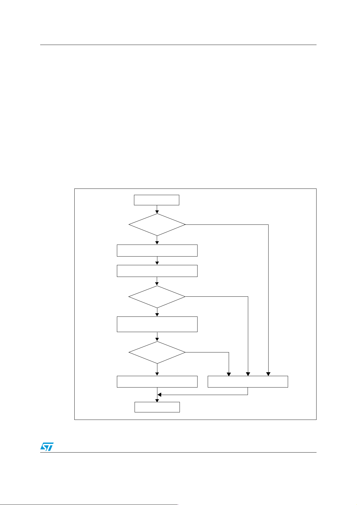
1.6 SystemMemory code program flow
Figure 11. SystemMemory code program flow
Start
Falling Edge on
UART0 Rx ?
Start Timer Base
No
All FLASH sectors
accessible except
SystemMemory sector
-
-
No
Falling Edge on
UART0 Rx ?
Stop Timer Base
Initialize UART0
Send Acknowledge
Clear the bit 22 of
the Flash Control
Register (Remap)
Done
Wait for a command
17/24
Page 18

General description AN2430
Figure 11 shows the program flow of the SystemMemory code. A few points worth noting
are:
● Not all the commands are available when readout protection is active, for more details
about the allowed commands please refer the section Readout Permanent Protect
command.
● The UART interface is only initialized if UART boot mode is detected.
Note: The STR75x Timer Base (TB) is used to automatically detect the serial baud rate. Once
initialized the UART configuration is 8-bits, No Parity, and 1 Stop bit.
18/24
Page 19

AN2430 UART SystemMemory boot mode
2 UART SystemMemory boot mode
2.1 UART SystemMemory code sequence
After SystemMemory mode is entered and the STR75x is configured as described above,
the SystemMemory code begins to scan the RxD0 line, waiting to receive a 0x7F data. (One
start bit, 0x7F data bits, and one stop bit).
The duration of this data byte is measured using the Timer Base. The count value of the
timer is then used to calculate the corresponding baud rate factor with respect to the current
system clock.
Next, the code initializes the serial interface accordingly, and sets up pin TxD0 to an
alternate function, push-pull output. Using this calculated baud rate, an acknowledge byte is
returned to the host which signals that the STR75x is ready to receive user commands.
Note: The acknowledge byte is 0x75 for the STR75x devices.
2.2 Choosing the UART baud rate
The calculation of the serial baudrate for UART0, from the length of the first byte that is
received, allows the operation of the STR75x SystemMemory bootloader within a wide
range of baud rates. However, the upper and lower limits have to be kept, in order to ensure
proper data transfer.
Baud Rate Divider = F
The STR75x uses the Timer Base to measure the length of the initial byte. The quantization
uncertainty of this measurement implies the first deviation from the theoretical baud rate.
The next deviation is implied by the computation of the Baud Rate Divider reload value from
the timer contents. The formula below shows the association:
TB_CNT / 8 = 1 Bit Time in F
Baud Rate Divider = TB_CNT / 8 / 16 = TB_CNT / 128
/ (16 * STR75x Baud Rate)
cpu
(8 Bit Times the first byte)
cpu
For a correct data transfer from the host to the STR75x, the maximum deviation between the
internal initialized baud rate for UART0 and the real baud rate of the host should be below
2.5%. The deviation (f
B
be calculated via the formula below:
f
= abs( (STR75x Baud Rate - Host Baud Rate) / STR75x Baud Rate) * 100%
B
f
<= 2.5%
B
Note: Function (f
) does not consider the tolerances of oscillators and other devices supporting
B
the serial communication.
This baud rate deviation is a non linear function depending on the CPU clock and the baud
rate of the host. The maximum of the function (f
due to the smaller baud rate pre-scale factors, and the implied higher quantization error.
2.2.1 Minimum baud rate
B
is the minimum baud rate determined by the maximum count capacity of Timer Base
Low
when measuring the first byte. This will be directly related to system clock frequency. Using
the maximum TB_CNT value of 65535 in the equations above we end up with a minimum
, in percent) between the host baud rate and STR75x baud rate can
) increases with the host baud rate. This is
B
19/24
Page 20

UART SystemMemory boot mode AN2430
Baud Rate of 1220 at F
2400. Baud rates below B
= 10MHz. The lowest standard Baud Rate for this case would be
cpu
would cause TB to overflow. If this occurs, it would not be
Low
possible to properly initialize the UART0.
2.2.2 The maximum baud rate
B
is the highest baud rate in which the deviation still does not exceed the limit. All baud
High
rates between B
Low
and B
are below the deviation limit.
High
Using the minimum TB_CNT value of 1in the equations above we end up with a maximum
Baud Rate of 125000 at F
= 2MHz. The highest standard Baud Rate for this case would
cpu
be 115000.
2.2.3 Higher baud rate deviations
A baud rate may be used as long as the actual deviation does not exceed the limit. Certain
lower baud rates may violate the deviation limit, while an even higher baud rates stays very
well below it. This relationship depends on the host interface.
20/24
Page 21

AN2430 Conclusion
3 Conclusion
The STR75x SystemMemory loader provides a convenient method for downloading user
code into on chip memories for a variety of applications. The UART interface provides an
easy and inexpensive, readily available serial link for desktop users.
21/24
Page 22

Bootloader availability limitations AN2430
4 Bootloader availability limitations
The bootloader feature is unavailable on some devices soldered on development tools
(starter kits or evaluation boards). Please check the date code written on the device. This
date code consists of 3 digits and is located as shown in Figure 12 below. If the device
soldered on the board displays a date code below 636, the bootloader feature is not
activated.
Note: If available, the bootloader version number (currently at V1.1) can be obtained through the
use of the Get command. Refer to Section 1.4.1 on page 5 for further details.
ST wants to highlight that this issue ONLY impacts devices soldered on a development tool
with the affected date codes. Any sample ordered separately from ST (or its distributors) has
the bootloader feature enabled (even if date code is below 636).
To those affected by this issue, ST offers the following recommendations:
● Use STR750 samples ordered separately (for example for building application
prototypes) to test the bootloader functionality.
● Use the free sample service from www.st.com . From the home page, type the correct
order code in the "Search Part #" field. From the results page, click the green
"Samples" button and follow the procedure. If the "Samples" button is not available, the
stock is in the process of being renewed and can be checked again at a later date.
● For further options or information, please contact your local distributor or ST sales
office.
Figure 12. Datecode marking on device
A
B
CD
F
a
E
G
J
HI
L
Areas H and I on the device marking
represent the date code in the following
manner:
● H: Year (Y)
● I: Week (WW)
22/24
Page 23

AN2430 Revision history
5 Revision history
Date Revision Changes
27-Sep-2006 1 Initial release
1-Dec-2006 2 Section 4: Bootloader availability limitations on page 22 added
08-Jan-2007 3
All references to GPIO0.4 pin removed
Section 1.7 removed
23/24
Page 24

AN2430
Please Read Carefully:
Information in this document is provided solely in connection with ST products. STMicroelectronics NV and its subsidiaries (“ST”) reserve the
right to make changes, corrections, modifications or improvements, to this document, and the products and services described herein at any
time, without notice.
All ST products are sold pursuant to ST’s terms and conditions of sale.
Purchasers are solely responsible for the choice, selection and use of the ST products and services described herein, and ST assumes no
liability whatsoever relating to the choice, selection or use of the ST products and services described herein.
No license, express or implied, by estoppel or otherwise, to any intellectual property rights is granted under this document. If any part of this
document refers to any third party products or services it shall not be deemed a license grant by ST for the use of such third party products
or services, or any intellectual property contained therein or considered as a warranty covering the use in any manner whatsoever of such
third party products or services or any intellectual property contained therein.
UNLESS OTHERWISE SET FORTH IN ST’S TERMS AND CONDITIONS OF SALE ST DISCLAIMS ANY EXPRESS OR IMPLIED
WARRANTY WITH RESPECT TO THE USE AND/OR SALE OF ST PRODUCTS INCLUDING WITHOUT LIMITATION IMPLIED
WARRANTIES OF MERCHANTABILITY, FITNESS FOR A PARTICULAR PURPOSE (AND THEIR EQUIVALENTS UNDER THE LAWS
OF ANY JURISDICTION), OR INFRINGEMENT OF ANY PATENT, COPYRIGHT OR OTHER INTELLECTUAL PROPERTY RIGHT.
UNLESS EXPRESSLY APPROVED IN WRITING BY AN AUTHORIZED ST REPRESENTATIVE, ST PRODUCTS ARE NOT
RECOMMENDED, AUTHORIZED OR WARRANTED FOR USE IN MILITARY, AIR CRAFT, SPACE, LIFE SAVING, OR LIFE SUSTAINING
APPLICATIONS, NOR IN PRODUCTS OR SYSTEMS WHERE FAILURE OR MALFUNCTION MAY RESULT IN PERSONAL INJURY,
DEATH, OR SEVERE PROPERTY OR ENVIRONMENTAL DAMAGE. ST PRODUCTS WHICH ARE NOT SPECIFIED AS "AUTOMOTIVE
GRADE" MAY ONLY BE USED IN AUTOMOTIVE APPLICATIONS AT USER’S OWN RISK.
Resale of ST products with provisions different from the statements and/or technical features set forth in this document shall immediately void
any warranty granted by ST for the ST product or service described herein and shall not create or extend in any manner whatsoever, any
liability of ST.
ST and the ST logo are trademarks or registered trademarks of ST in various countries.
Information in this document supersedes and replaces all information previously supplied.
The ST logo is a registered trademark of STMicroelectronics. All other names are the property of their respective owners.
© 2007 STMicroelectronics - All rights reserved
STMicroelectronics group of companies
Australia - Belgium - Brazil - Canada - China - Czech Republic - Finland - France - Germany - Hong Kong - India - Israel - Italy - Japan -
Malaysia - Malta - Morocco - Singapore - Spain - Sweden - Switzerland - United Kingdom - United States of America
www.st.com
24/24
 Loading...