

Page 1

AN2419
Application note
STR75x hardware development
getting started
Introduction
This application note is intended for system designers who require a hardware
implementation overview of the development board features such as the power supply, the
clock management, the reset control, the boot mode settings and the debug management. It
shows how to use the STR75x product family and describes the minimum hardware
resources required to develop an STR75x application.
Detailed reference design schematics are also contained in this document with descriptions
of the main components, interfaces and modes.
July 2007 Rev 2 1/22
www.st.com
Page 2

Contents AN2419
Contents
1 Power supplies . . . . . . . . . . . . . . . . . . . . . . . . . . . . . . . . . . . . . . . . . . . . . 4
1.1 Introduction . . . . . . . . . . . . . . . . . . . . . . . . . . . . . . . . . . . . . . . . . . . . . . . . 4
1.2 Power supply schemes . . . . . . . . . . . . . . . . . . . . . . . . . . . . . . . . . . . . . . . . 4
1.2.1 Power scheme 1: single external 3.3V power source . . . . . . . . . . . . . . . 4
1.2.2 Power scheme 2: dual external 3.3V and 1.8V power sources . . . . . . . . 5
1.2.3 Power scheme 3: single external 5V power source . . . . . . . . . . . . . . . . . 6
1.2.4 Power scheme 4: dual external 5.0V and 1.8V power sources . . . . . . . . 7
1.3 Reset and power startup . . . . . . . . . . . . . . . . . . . . . . . . . . . . . . . . . . . . . . 7
1.3.1 Power startup specifications . . . . . . . . . . . . . . . . . . . . . . . . . . . . . . . . . . 7
1.3.2 External reset . . . . . . . . . . . . . . . . . . . . . . . . . . . . . . . . . . . . . . . . . . . . . . 8
2 Clocks . . . . . . . . . . . . . . . . . . . . . . . . . . . . . . . . . . . . . . . . . . . . . . . . . . . . . 9
2.1 Clock overview . . . . . . . . . . . . . . . . . . . . . . . . . . . . . . . . . . . . . . . . . . . . . . 9
2.2 Main 4MHz or 8MHz oscillator (OSC4M) . . . . . . . . . . . . . . . . . . . . . . . . . 10
2.3 Low power 32.768 kHz oscillator (OSC32K) . . . . . . . . . . . . . . . . . . . . . . 11
2.4 USB clock . . . . . . . . . . . . . . . . . . . . . . . . . . . . . . . . . . . . . . . . . . . . . . . . . 11
2.5 PLL, FREEOSC, and AHB/APB prescalers . . . . . . . . . . . . . . . . . . . . . . . 12
2.6 Clock-out capability: MCO (Main Clock Output) . . . . . . . . . . . . . . . . . . . . 13
2.7 Clock detector (CKD) . . . . . . . . . . . . . . . . . . . . . . . . . . . . . . . . . . . . . . . . 13
3 Boot configuration . . . . . . . . . . . . . . . . . . . . . . . . . . . . . . . . . . . . . . . . . 14
3.1 Embedded boot loader mode . . . . . . . . . . . . . . . . . . . . . . . . . . . . . . . . . . 15
3.2 External memory (SMI) boot mode . . . . . . . . . . . . . . . . . . . . . . . . . . . . . 15
4 Debug management . . . . . . . . . . . . . . . . . . . . . . . . . . . . . . . . . . . . . . . . 16
4.1 ICE debug tool . . . . . . . . . . . . . . . . . . . . . . . . . . . . . . . . . . . . . . . . . . . . . 16
4.2 JTAG / ICE connector . . . . . . . . . . . . . . . . . . . . . . . . . . . . . . . . . . . . . . . . 16
5 Reference design . . . . . . . . . . . . . . . . . . . . . . . . . . . . . . . . . . . . . . . . . . 19
5.1 Main . . . . . . . . . . . . . . . . . . . . . . . . . . . . . . . . . . . . . . . . . . . . . . . . . . . . . 19
5.1.1 Clock . . . . . . . . . . . . . . . . . . . . . . . . . . . . . . . . . . . . . . . . . . . . . . . . . . . 19
5.1.2 Reset . . . . . . . . . . . . . . . . . . . . . . . . . . . . . . . . . . . . . . . . . . . . . . . . . . . 19
5.1.3 Boot mode . . . . . . . . . . . . . . . . . . . . . . . . . . . . . . . . . . . . . . . . . . . . . . . 19
2/22
Page 3

AN2419 Contents
5.2 JTAG interface . . . . . . . . . . . . . . . . . . . . . . . . . . . . . . . . . . . . . . . . . . . . . 19
6 Schematics . . . . . . . . . . . . . . . . . . . . . . . . . . . . . . . . . . . . . . . . . . . . . . . 20
7 Revision history . . . . . . . . . . . . . . . . . . . . . . . . . . . . . . . . . . . . . . . . . . . 21
3/22
Page 4

Power supplies AN2419
1 Power supplies
1.1 Introduction
The device has five power pins:
● V
STANDBY mode.
● V
SRAM and Flash: 1.8V ± 0.15V.
● V
Two embedded regulators are available to supply the internal 1.8V digital power:
V
and V
18
The Main Voltage Regulator (MVREG) supplies V
of 1.8V ± 0.15V.
: power supply for I/Os (3.3V ±0.3V or 5V ±0.5V). Must be kept on, even in
DD_IO
(pins V
18
: Backup Power Supply for STANDBY or STOP Mode
18_BKP
18_BKP
and V18 which are internally shorted): Power Supply for Digital,
18REG
are normally generated internally by these regulators.
18
and V
. It delivers a power supply
18_BKP
The Low Power Voltage Regulator (LPVREG) can supply V
18_BKP
STANDBY mode. It delivers a power supply of around 1.4V.
Two sensitive analog blocks have dedicated power pins:
● V
● V
DDA_PLL
DDA_ADC
: Analog Power supply for PLL (must have the same voltage level as V
: Analog Power supply for ADC (must have the same voltage level as V
1.2 Power supply schemes
The device can be connected in any of the following configurations depending on your
application requirements:
● Power Scheme 1: Single external 3.3V power source
● Power Scheme 2: Dual external 3.3V and 1.8V power sources
● Power Scheme 3: Single external 5.0V power source
● Power Scheme 4: Dual external 5.0V and 1.8V power sources
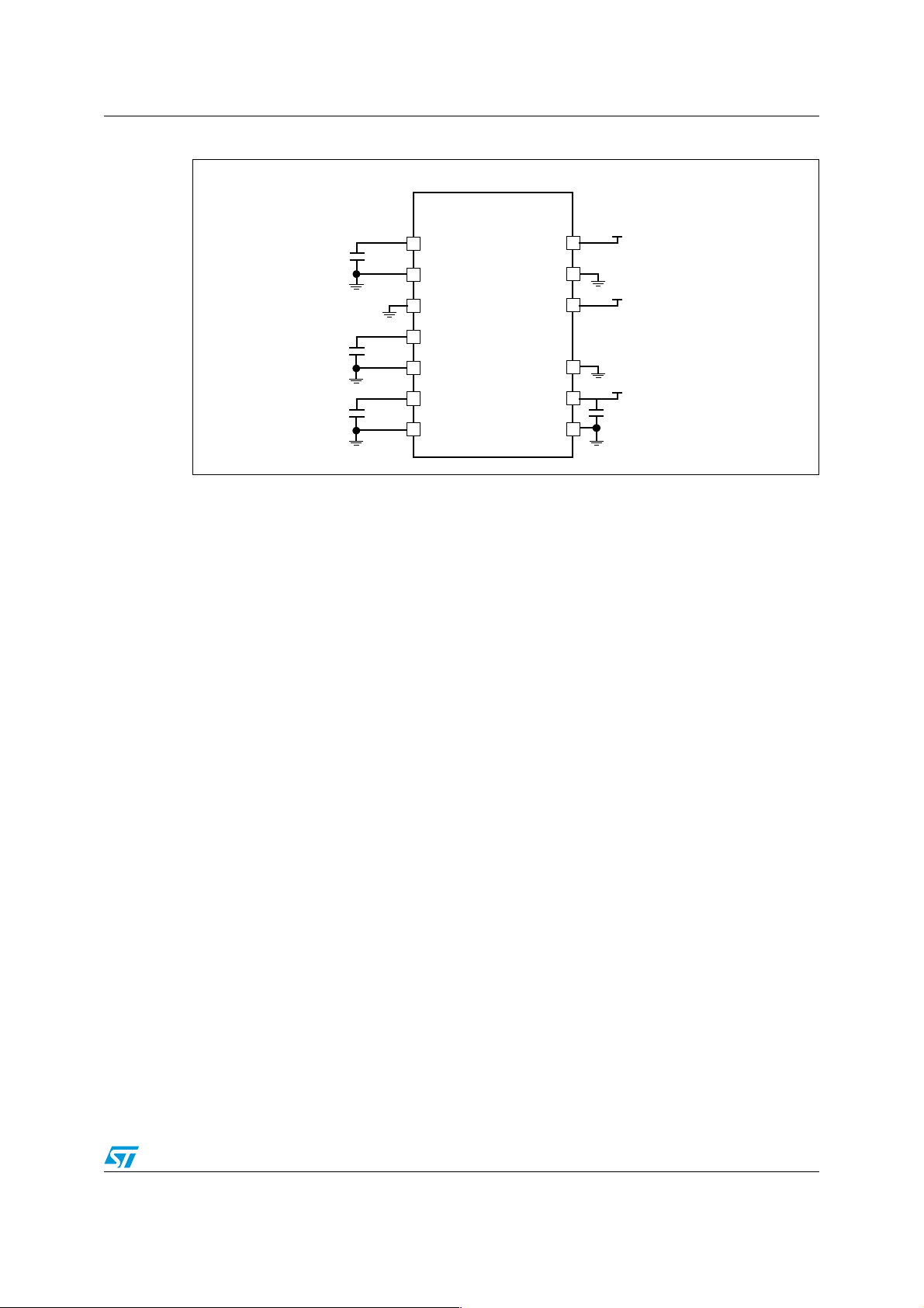
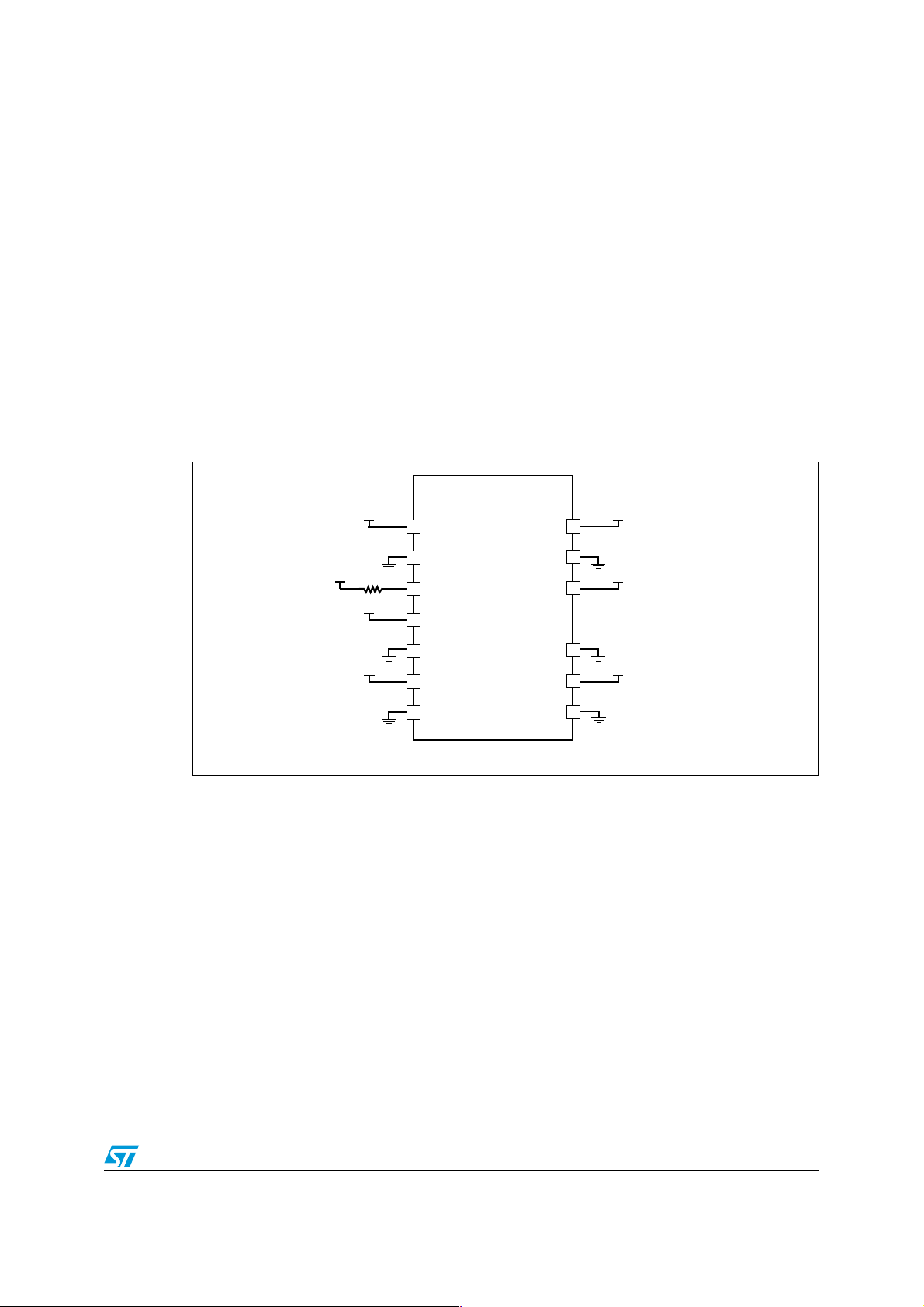
1.2.1 Power scheme 1: single external 3.3V power source
In this configuration, the internal voltage regulators are switched on by forcing the
VREG_DIS pin to low level.
● The V
Tantalum, low series resistance).
● The V
● The V
● A decoupling capacitor of 1µF must be added on the V
V
18REG
pin must be connected to external stabilization capacitors (min. 10 uF
18REG
pin must be connected to external stabilization capacitors (33nF ceramic).
18
pin must be connected to an external stabilization capacitor of 1µF.
18_BKP
DD_IO
pin.
or V18 in STOP or
DD_IO
DD_IO
pin which is closest to the
)
)
4/22
Page 5
AN2419 Power supplies
Figure 1. Power supply scheme 1 (single 3.3V supply, VREGDIS=0) in NORMAL mode
STR750
+3.3V
+3.3V
+3.3V
1µF
1µF
33nF
10µF
V
18_BKP
V
SS_BKP
VREG_DIS
V
18
V
SS18
V
18REG
V
SS18
V
DD_PLL
V
SS_PLL
V
DD_ADC
V
SS_ADC
V
DD_IO
V
SS_IO
1.2.2 Power scheme 2: dual external 3.3V and 1.8V power sources
In this configuration, the internal voltage regulators are switched off by forcing the
VREG_DIS pin to high level. This scheme has the advantage of saving power consumption
when the 1.8V power supply is already available in the application. V
provided externally through the V
● The external 3.3V power supply must always be kept on.
● VREG_DIS pin is tied to high level which disables the Main Voltage Regulator and
18REG
, V18 and V
18_BKP
power pins.
the Low Power Voltage Regulator.
18
and V
18_BKP
are
Caution: When powered by 5.0V, the USB peripheral cannot operate.
● All digital power pins (V
18REG
, V18 and V
) must be externally shorted to the
18_BKP
same 1.8V power supply source.
● In this scheme, STANDBY Mode is not available.
5/22
Page 6
Power supplies AN2419
Figure 2. Power supply scheme 2 (3.3V and 1.8V supplies, VREGDIS=1)
STR750
V
V
18_BKP
V
+3.3V
+1.8V
+1.8V
NOTE : THE EXTERNAL 3.3V POWER SUPPLY MUST ALWAYS BE KEPT ON
SS_BKP
VREG_DIS
V
18
V
SS18
V
18REG
V
SS18
DD_PLL
V
SS_PLL
V
DD_ADC
V
SS_ADC
V
DD_IO
V
SS_IO
+3.3V+1.8V
+3.3V
+3.3V
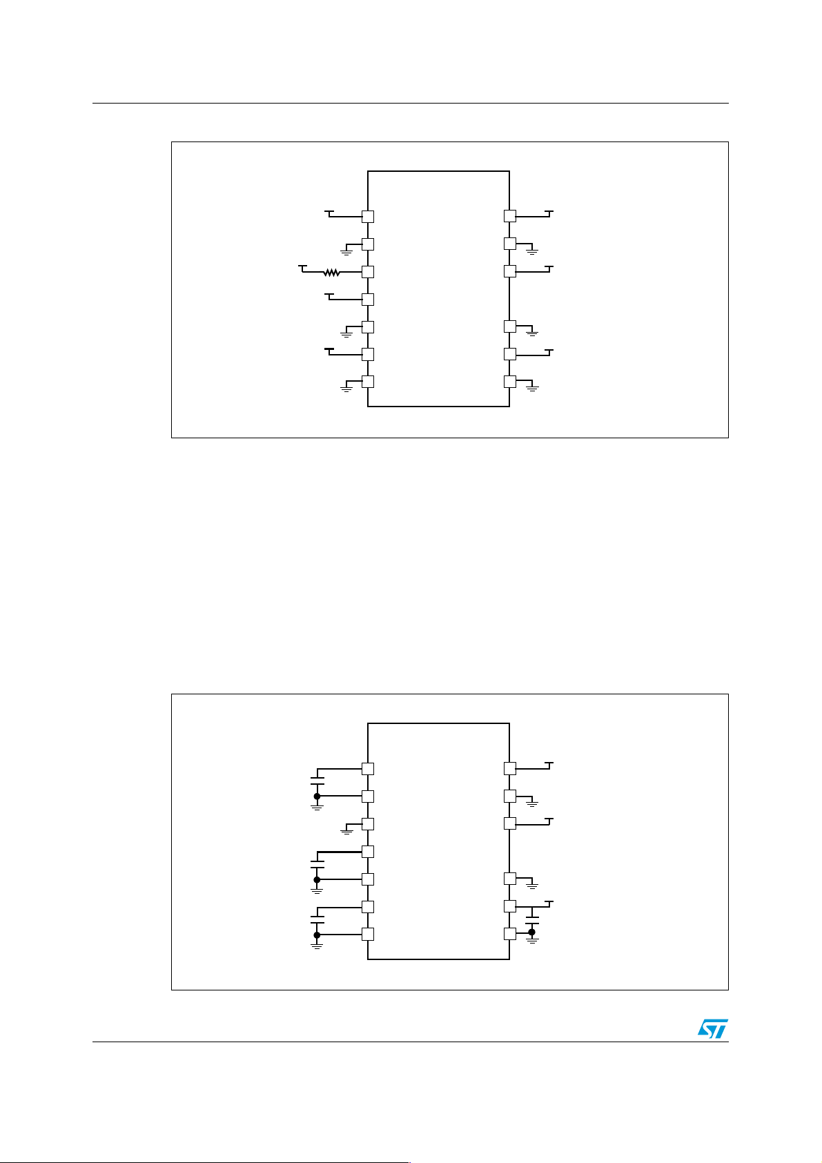
1.2.3 Power scheme 3: single external 5V power source
In this configuration, the internal voltage regulators are switched on by forcing the
VREG_DIS pin to low level.
● The V
pin must be connected to external stabilization capacitors (min. 10 uF
18REG
Tantalum, low series resistance).
● The V
● The V
● A decoupling capacitor of 1µF must be added on the V
V
pin must be connected to external stabilization capacitors (33nF ceramic).
18
pin must be connected to an external stabilization capacitor of 1µF.
18_BKP
DD_IO
pin.
18REG
Caution: When powered by 5.0V, the USB peripheral cannot operate.
Figure 3. Power supply scheme 3(single 5V supply, VREGDIS=0) in NORMAL mode
STR750
+5V
+5V
+5V
1µF
1µF
33nF
10µF
V
18_BKP
V
SS_BKP
VREG_DIS
V
18
V
SS18
V
18REG
V
SS18
V
DD_PLL
V
SS_PLL
V
DD_ADC
V
SS_ADC
V
DD_IO
V
SS_IO
pin which is closest to the
6/22
Page 7
AN2419 Power supplies
1.2.4 Power scheme 4: dual external 5.0V and 1.8V power sources
In this configuration, the internal voltage regulators are switched off, by forcing the
VREG_DIS pin to high level. This scheme has the advantage of saving power consumption
when the 1.8V power supply is already available in the application and providing 5V I/O
capability. V
power pins.
● VREG_DIS pin is tied to high level which disables the Main Voltage Regulator and the
Low Power Voltage Regulator.
● All digital power pins (V
same 1.8V power supply source.
In this scheme:
● STANDBY Mode is not available
● USB functionality is not available
Figure 4. Power supply scheme 4 (5.0V and 1.8V supplies, VREGDIS=1)
18
and V
18_BKP
+5.0V
are provided externally through the V
18REG
, V18 and V
) must be externally shorted to the
18_BKP
STR750
+1.8V
+1.8V
+1.8V
V
18_BKP
V
SS_BKP
VREG_DIS
V
18
V
SS18
V
18REG
V
SS18
V
DD_PLL
V
SS_PLL
V
DD_ADC
V
SS_ADC
V
DD_IO
V
SS_IO
+5.0V
+5.0V
+5.0V
18REG
, V18 and V
18_BKP
NOTE : THE EXTERNAL 5.0V POWER SUPPLY MUST ALWAYS BE KEPT ON
1.3 Reset and power startup
1.3.1 Power startup specifications
To ensure the MCU starts-up cleanly, the rise time of the V
comprised between 20µs/V and 20ms/V.
In addition, you must provide an external RESET for at least 20µs after the V
supply has reached its minimum working value (3.0V). It is recommended to use an external
Power-On-Reset circuit monitoring V
During V
state, assuming external RESET is asserted.
If you are using an external 1.8V power supply, the rise time of power supply V
comprised between 20µs/V and 20ms/V.
power-up (from 0V to 3.3V or 5.0V), all I/Os are guaranteed to be in HiZ
DD_IO
power supply must be
DD_IO
power
DD_IO
to assert the RESET at power-up .
DD_IO
must be
18
7/22
Page 8

Power supplies AN2419
1.3.2 External reset
The NRSTIN pin acts as an asynchronous RESET active low.
The NRSTIN pad input is a Schmitt Trigger input pin. A filter is added to ignore all incoming
pulses with short duration:
● All negative spikes with a duration less than 150ns are filtered.
● All trains of negative spikes with a ratio of 1/2 are filtered. This means that all spikes
with a maximum duration of 150ns with minimum interval between spikes of 75ns are
filtered.
● An internal pull up is connected on each of the pins NRSTIN and NRSTOUT.
An external reset circuit can be connected (STM1818) to manage the reset signal: both for
power-on reset during startup and management of the reset button (debounce functionality
and pulse duration control).
Figure 5. Reset circuit
EXTERNAL
V
DD
RESET
V
CC
V
SS
STM1818
STM1813*
* use STM1818TWX7F if VDD=3.3V
use STM1813LWX7F if VDD=5.0V
STR750
RST
NRSTIN
NRSTOUT
V
V
DD_IO
R
DD_IO
PU
R
PU
The NRSTOUT pin is an exact image of the system Reset signal (active low) provided to the
device which is used to generate the reset of the AHB System and the reset of each APB
peripherals. Internal circuitry guarantees a minimum reset pulse duration of 20µs.
Some peripheral registers, like the RTC or the BACKUP registers are not reset by a System
Reset but only by an RSM Reset: this means that these registers are only reset at VDD
power up. For more details see the Reference manual UM0191.
8/22
Page 9

AN2419 Clocks
2 Clocks
2.1 Clock overview
Figure 6. Clock overview
XT1
XT2
XRTC1
XRTC2
USB_CK
PLL
FREEOSC
OSC4M
OSC32K
LPOSC
4MHz
CLOCK
DETECTOR
/128
32kHz
300kHz
PLL
1-10 MHz
UP TO 64 MHz
48 MHz
CKD FLAG
CKD FLAG
RTC
HCLK
CK_SYS
ALARM
WAKEUP
For further details see the Reference manual UM0191.
AHB & APB
DIVIDERS
UP TO 64MHz
PCLK
UP TO 32MHz
CK_TIM
UP TO 64MHz
CK_USB
48 MHz
Several on-chip oscillators can feed the MCU system clock (CK_SYS) from which the HCLK
and PCLK derive:
● FREEOSC: Internal Free Running Oscillator providing a clock between 1 and 10MHz,
also used as emergency clock. It consists of the internal VCO of the PLL configured in
free running mode
● OSC4M: 4MHz or 8MHz Main Oscillator (Crystal or Ceramic oscillator or external
clock)
– a 4 MHz Crystal/Ceramic oscillator connected to XT1/XT2
– or an 8 MHz Crystal/Ceramic oscillator to XT1/XT2 followed by a divider by 2
– or external clock connected to XT1
● OSC32K: 32.768kHz Oscillator (Crystal or Ceramic oscillator) which can drive either
the system clock and/or the RTC.
● LPOSC: Internal Low Power RC Oscillator providing a clock around 300kHz which can
drive either the system clock and/or the RTC.
Several configurable dividers provide a high degree of flexibility to the application in the
choice of the APB or AHB frequency, while keeping a fixed frequency value for the USB
clock (48 MHz).
9/22
Page 10

Clocks AN2419
The Clock Detector (CKD) protects the Microcontroller against OSC4M or external clock
failures.
The RTC provides calender, alarm and wake-up functions and can be clocked by any of the
oscillators other than FREEOSC.
Caution: The FREEOSC and PLL are reset during the whole assertion of System RESET. After reset
release, the PLL is disabled and FREEOSC supplies the system clock (1-10 MHz).
2.2 Main 4MHz or 8MHz oscillator (OSC4M)
XT1 and XT2 pins are used to connect the Main Oscillator source, which can be a resonator
(crystal or ceramic) or an external source. Both sources can be used as the input clock to
PLL frequency multiplier (PLL).
Crystal or ceramic resonator
This 4 MHz oscillator (OSC4M) has the advantage of producing a very accurate rate on the
main clock. This oscillator can be directly connected to
● a 4 MHz Oscillator
● or an 8 MHz Oscillator followed by an internal divider by 2.
If an 8 MHz Crystal or Ceramic is connected, You must select the divider by 2
The associated hardware configuration are shown in Figure 7. Refer to the electrical
characteristics section of the datasheet for more details.
Figure 7. Clock sources
Hardware Configuration
STR7
XT1 XT2
(HiZ)
External ClockCrystal/Ceramic Resonators
EXTERNAL
SOURCE
STR7
XT1 XT2
C
L1
LOAD
CAPACITORS
C
L2
The resonator and the load capacitors have to be placed as close as possible to the
oscillator pins in order to minimize output distortion and start-up stabilization time. The
loading capacitance values must be adjusted according to the selected oscillator.
10/22
Page 11

AN2419 Clocks
External Source (Bypass Mode)
In this mode, an external clock source must be provided. The external clock signal (square,
sinus or triangle) with ~50% duty cycle has to drive the XT1 pin while the XT2 pin should be
left hi-Z.
2.3 Low power 32.768 kHz oscillator (OSC32K)
XRTC1 and XRTC2 pins are used to connect the 32k Oscillator source, which can be a
resonator (crystal or ceramic).The OSC32k clock can be used as a low power system clock
Figure 8. Clock sources
Hardware Configuration
STR7
XRTC1 XRTC2
Crystal/Ceramic Resonators
The resonator and the load capacitors have to be placed as close as possible to the
oscillator pins in order to minimize output distortion and start-up stabilization time. The
loading capacitance values must be adjusted according to the selected oscillator.
2.4 USB clock
STR75x series microcontrollers contain a USB 2.0 Full Speed device module interface that
operates at a precise frequency of 48 MHz. This clock is usually generated by the internal
PLL using one single external oscillator for both the system and USB module to save board
space and cost. However, if the chosen system clock is not compatible with the 48 MHz
clock generation (frequency below 48 MHz), the USB clock can also provided by an external
oscillator connected to the USB clock pin USBCLK.
The following diagram shows the basic implementation of the USB external clock.
Figure 9. USB clock oscillator
3V3
OSCILLATOR
48MHz
C
L1
LOAD
CAPACITORS
STR75x
C
L2
OSC_OUT
USB_CK
VSS
11/22
Page 12

Clocks AN2419
2.5 PLL, FREEOSC, and AHB/APB prescalers
Figure 10. PLL, FREEOSC & AHB/APB prescaler scheme
OSC4M
4MHz
CK_OSC4M
FREEOSC
PLL
LOCK
PLLEN
MX[1:0]
RANGE
PLLEN
NCKDF
1-10MHz
UP TO 64MHz
48MHz
CK_RTC
CK_OSC4M
1
0
CKOSCSEL
1
0
CK_PLL1
UP TO 64MHz
CK_PLL2
48MHz
4MHz
CKSEL
1
0
CK_SYS
HPRESC[1:0]
AHB PRESC
/1,2,4 or 8
PPRESC[1:0]
APB PRESC
/1,2,4 or 8
PPRESC[2]
1
/2
0
HCLK
UP TO 64MHz
PCLK
UP TO 32MHz
CK_TIM
UP TO 64MHz
USB_CK
48MHz
The CPU can execute:
● the SRAM up to 64 MHz at zero wait state.
● the Flash up to 60 MHz speed in burst mode (zero wait state for consecutive accesses,
1 wait state for any non-consecutive access)
● the Flash up to 32 MHz at zero wait state
The PLL provides a Frequency Multiplier starting from a single input clock (OSC4M source)
and providing the 2 following independent output clocks:
● CK_PLL1 output with 4 programmable multiplication factors (up to 64 MHz) used for
generating CK_SYS
● CK_PLL2 output with fixed 48 MHz frequency when input clock is 4 MHz used for
generating CK_USB
FREEOSC provides a Free Running Oscillator for the system clock: this clock is selected
when:
● The PLL is disabled: FREEOSC acts as an oscillator source
● The clock failure flag is active: FREEOSC acts as an emergency clock source.
For security, hardware prevents the software from making certain unrecoverable errors:
● Software cannot switch CK_SYS to CK_PLL1 (multiplied clock output) until the PLL is
locked.
● CK_USB is gated until the software enables the PLL2EN bit in the MRCC_CLKCTL
register.
12/22
Page 13

AN2419 Clocks
The AHB and APB prescalers allow you to choose the AHB and APB frequencies from a
wide range of possibilities:
● HCLK (AHB Clock) can be generated from CK_SYS divided by 1, 2, 4 or 8
● PCLK (APB Clock) can be generated from HCLK divided by 1, 2, 4, 8 or 16
The clock provided to the Timers (CK_TIM) can have twice or the same frequency as PCLK.
This allows the timers to count at high frequency (up to 64MHz)
Ta bl e 1 gives some typical clock configurations:
Table 1. Typical prescaler uses
f
OSC4M
(MHz)
PLL
Factor
f
CK_SYS
(MHz)
HPRESC
[1:0]
f
HCLK
(MHz)
PPRESC
[1:0]
f
CK_TIM
(MHz)
PPRESC2
f
PCLK
(MHz)
f
CK_USB
(MHz)
x16 64 00 64
00 64
01 32 16
x15 60 00 60 00 60 30
4
x14 56 00 56 00 56 28
x12 48 00 48 00 48 24
x16 64 01 32 00 32 16
The software must respect the configuration constraints of the PLL.
2.6 Clock-out capability: MCO (Main Clock Output)
The Main Clock Output (MCO) capability allows you to output a clock on the external MCO
pin. The configuration registers of corresponding GPIO port must programmed in alternate
function mode. You can select one of 4 clock signals as MCO clock.
● CK_PLL2
● HCLK
● PCLK
● CK_OSC4M
The selection is controlled by the MCOS[1:0] bits of CLKCTL register. A dedicated prescaler
(divide by 1 or 2, selected by MCOP bit) can be applied to this clock before outputting it to
the MCO pin. Care must be taken when switching MCO clock selection, the alternate
function should be disabled to avoid any glitches on the MCO pin.
32
1
48
2.7 Clock detector (CKD)
A CKD (Clock Detector) is implemented to:
● detect if no clock is present on OSC4M (broken or disconnected resonator) and prevent
the software from selecting it.
● automatically feeds the MCU with the FREEOSC used as emergency clock if no clock
is detected.
● generate an interrupt if enabled, allowing the MCU to perform some rescue operations
For more detail see the Reference Manual (UM0191).
13/22
Page 14

Boot configuration AN2419
3 Boot configuration
In the STR750, 4 different boot modes can be selected by means of the BOOT[1:0] pins as
shown in Ta bl e 2 .
Table 2. Boot modes
BOOT Mode
Selection Pins
BOOT1 BOOT0
Boot Mode Aliasing Note
0 0 Embedded Flash
1 0 Embedded SRAM
0 1 SystemMemory
11
External SMI Serial Flash
memory
Embedded FLASH sector
B0F0 mapped at 0h
Embedded SRAM mapped
at 0h
SystemMemory mapped
at 0h
SMI Bank 0 mapped at 0h -
All FLASH sectors
accessible except
SystemMemory
sector
-
Figure 11. Boot mode selection implementation example
STR75x
3V3
* these values are given only as typical example
10K*
3V3
10K*
BOOT0
BOOT1
TEST
GND
This aliases the physical memory associated with each boot mode to Block 000 (boot
memory).The value of the BOOT pin is latched on the 4th rising edge of CK_SYS after
Reset.
It is up to the user to manage the BOOT1 and BOOT0 pins at reset release to select the
required boot mode. Note that the user should also manage these pins when exiting
Standby mode as the BOOT pins are resampled.
Even when aliased in the boot memory space, the related memory (FLASH, SRAM or SMI)
is still accessible at its original memory space.
After this start-up delay has elapsed, the ARM CPU will start code execution from the boot
memory space, located at the bottom of the memory space starting from 0x0000_0000h.
The application can read the status of the boot pins that was latched at start-up and change
the memory aliasing on-the-fly by modifying the SW_BOOT bits in the CFG_GLCONF
register.
Caution: The TEST pin of the STR75x must always be forced to ground (ST reserved test pin)
14/22
Page 15

AN2419 Boot configuration
3.1 Embedded boot loader mode
Embedded Boot Loader Mode is used to re-program the FLASH using one of the serial
interfaces (typically a UART). This program, called, ICP boot loader, is located in the
SystemMemory and is programmed by ST during production.
Refer to the STR7 Family Flash Programming Reference Manual for details.
3.2 External memory (SMI) boot mode
When SMI boot mode is selected the Serial Memory Interface is automatically configured as
follows:
● Chip Select Polarity = low
● SMI bank 0 is selected and the associated I/O alternate functions are enabled.
● Boot Space (0000_0000h to 00FF_FFFFh -16MB) is aliased to SMI bank 0.
● The SMI is configured as NORMAL READ MODE (reset value)
● The SMI_PRESCALER is set to “2” (reset value)
Programming considerations when booting from SMI
After RESET, the PLL is disabled and both CK_SYS and HCLK are clocked by the internal
FREEOSC oscillator (1-10MHz). Consequently, the SMI clock output is also between 0.5
and 5MHz (SMI_PRESCALER reset state is 2). To use a higher frequency, software has to
configure the clock and PLLs.
Care is needed if the program performing the PLL and clock configuration is executed
directly from serial memory. The software must ensure that a proper clock frequency is
provided to the serial memory when changing the SMI_PRESCALER and switching the
system clock. That is why the SMI_PRESCALER must be changed first before switching the
system clock to the PLL output clock.
For example, to use the SMI in NORMAL READ MODE with a 60 MHz HCLK frequency, set
the SMI_PRESCALER to 4 before switching HCLK to 60 MHz. The SMI clock frequency is
then 60 MHz / 4 = 15 MHz.
It is possible to obtain the highest SMI frequency using the FAST READ MODE, if the serial
memory supports this mode. For instance, f
can be set to 48 MHz and the
HCLK
SMI_PRESCALER can be be loaded to "1" to address a high speed Serial Memory at 48
MHz (for read only).
Note: Make sure that the SMI clock frequency (resulting from of your AHB clock and
SMI_PRESCALER settings) does not exceed the maximum allowed value. The maximum
frequency of the SMI is limited by the I/O speed.
Take care to load the SMI_PRESCALER and the FAST_READ mode with the same write
transaction. This can be done by a program which is executed from the serial Flash. In this
case, the SMI will change the clock and the READ MODE only at the end of this access. For
more details refer to the Reference Manual.
15/22
Page 16

Debug management AN2419
4 Debug management
The Host/Target interface is the hardware equipment that connects the Host to the
application board. This interface is made of three components: a hardware debug tool, such
as Micro-ICE from ARM, a JTAG connector and a cable connecting the host to the debug
tool.
Figure 12 shows the connection of the host to the STR75x board.
Figure 12. Host to board connection
ICE Debug tool
ICE connector
HOST PC
4.1 ICE debug tool
ICE Debug tool is a host interface that connects a PC to an STR75x development board
featuring a debug interface as shown in Figure 12. The Embedded ICE is an intelligent host
interface that provides fast access to host services, access to on-chip emulation and debug
facilities. When the STR75x board is configured as a stand-alone system, the ICE Debug
tool can be used to download programs.
The STR75x development kit supports the ARM RealView ICE Micro Edition. The Micro-ICE
is plugged in to the host via a USB cable.
4.2 JTAG / ICE connector
The ICE connector enables JTAG hardware debugging equipment, such as RealView-ICE,
to be connected to the STR75x board. It is possible to both drive and sense the systemreset line, and to then send a JTAG reset to the core through the ICE connector. Figure 13
shows the ARM ICE connector pin-out.
The STR75x has a user debug interface. This interface contains a five-pin serial interface
conforming to JTAG, IEEE standard 1149.1-1993, “Standard Test Access Port-Scan
Boundary Architecture”. JTAG allows the ICE device to be plugged to the board and used to
debug the software running on the STR75x.
STR75x EVAL
Power
Supply
JTAG emulation allows the core to be started and stopped under the control of the
connected debugger software. The user can then display and modify registers and memory
contents, and set break and watch points.
16/22
Page 17

AN2419 Debug management
Figure 13. Ice connector implementation
3V3
3V3
STR75x
3V3
10K*10K*
nJTRST
JTDI
JTMS
JTCK
RTCK
JTDO
NRSTIN
10K*
* these values are given only as typical examples
J4
See
Note 1
3V3
Note: 1 The JTAG reset pin (nJTRST) is a dedicated pin:
When JTAG communication is used on the application board, nJTRST must be connected to
a pull-up. However, it is mandatory to apply one negative pulse on nJTRST pin after powerup otherwise the MCU may enter unexpected test modes. For instance, nJTSRT can be
connected to the system reset which is pulled-up.
When JTAG communication is not used on the application board, nJTRST can be connected
to the system reset or it can be also indefinitely grounded.
10K*
10K*
10K*
3V3
10K*
10K*
3V3
JTAG Connector CN9
CONN_2*10
(1)
VTref
(3) nTRST
(5) TDI
(7) TMS
(9) TCK
(11) RTCK
(13) TDO
(15) nSRST
(17) DBGRQ
(19) DBGACK
10K*
3V3
(2)
(4)
(6)
(8)
(10)
(12)
(14)
(16)
(18)
(20)
GND
Caution: When the internal Flash is readout protected, the Flash will not execute if nJRST is not
continuously reset because it is considered as an intrusion. Consequently, in this case, it is
mandatory that the nJRST pin sees a continuous low level after reset when the user
application is running.
17/22
Page 18

Debug management AN2419
Table 3. JTAG connector pins
Std
Name
STR75x Description Function
nTRST JTRST
TDI JTDI
TMS JTMS
TCK JTCK
RTCK RTCK
TDO JTDO
nSRST NRSTIN
Test Reset
(from JTAG
equipment)
Test data in
(from JTAG
equipment)
Test mode
select (from
JTAG
equipment)
Test clock (from
JTAG
equipment)
Return TCK (to
JTAG
equipment)
Test data out
(to JTAG
equipment)
System reset
(bidirectional)
This active LOW open-collector is used to reset the JTAG
port and the associated debug circuitry. It is asserted at
power-up by each module, and can be driven by the JTAG
equipment.
TDI goes down the stack of modules to the motherboard
and then back up the stack, labelled TDO, connecting to
each component in the scan chain.
TMS controls transitions in the tap controller state machine.
TMS connects to all JTAG components in the scan chain as
the signal flows down the module stack.
TCK synchronizes all JTAG transactions. TCK connects to
all JTAG components in the scan chain. Series termination
resistors are used to reduce reflections and maintain good
signal integrity. TCK flows down the stack of modules and
connects to each JTAG component. However, if there is a
device in the scan chain that synchronizes TCK to some
other clock, then all down-stream devices are connected to
the RTCK signal on that component.
Using a mechanism called adaptive clocking, the RTCK
signal is returned by the core to the JTAG equipment, and
the clock is not advanced until the core had captured the
data. In adaptive clocking mode, the debugging equipment
waits for an edge on RTCK before changing TCK.
TDO is the return path of the data input signal TDI.
nSRST is an active LOW open-collector signal that can be
driven by the JTAG equipment to reset the target board.
Some JTAG equipment senses this line to determine when
a board has been reset by the user.
When the signal is driven LOW by the reset controller on the
core module, the motherboard resets the whole system by
driving nSYSRST low.
For more details on the JTAG port refer to the IEEE standard 1149.1-1993, “Standard Test
Access Port-Scan Boundary Architecture” specification.
18/22
Page 19

AN2419 Reference design
5 Reference design
5.1 Main
This reference design is based on the STR750, a highly integrated microcontroller, running
at 64MHz that combines the popular ARM7TDMI-S
embedded Flash, 16Kbytes of high speed SRAM
5.1.1 Clock
Two clock sources are used for the microcontroller.
● X1-32 kHz crystal for embedded RTC
● X2-4 MHz crystal for STR750Fx microcontroller
5.1.2 Reset
The reset signal on this STR750-REF schematic is active low.
The reset sources include:
● Power On Reset from STM1818 (U2)
● Reset button (PB1)
● Debugging tools via the connector CN1
5.1.3 Boot mode
The STR750 is able to boot from:
● Embedded User Flash
● Embedded SRAM for debugging
● System memory with boot loader for ISP
● External SPI Interface Flash
TM
32-bit RISC CPU with 256 Kbytes of
.
The boot option is configured by setting switches SW1 (Boot 0) and SW2 (Boot 1).
5.2 JTAG interface
Refer to the section Section 4: Debug management on page 16.
19/22
Page 20

Schematics AN2419
6 Schematics
Figure 14. STR750F microcontroller connections
4
+3V3
3
1
SW1
2
R1
10K
P002
P001P101
P003
P004
P000
79
4
3
2
100
3
TIM2_TI1/P0.03
TIM2_OC1/P0.02
MCO/TIM0_TI1/P0.01
BOOT0/TIM0_OC1/P0.00
TIM2_TI2/P1.03
TIM2_OC2/P1.0268PWM_EMERG/P1.10
TIM0_TI2/P1.01
TIM0_OC2/P1.00
U1
67
91
94
95
2
P102
P103
P104
P100
+3V3+3V3
10KR310KR410KR510KR610KR810K
TRST
R2
TDI
1
3
SW2
2
R7
P010
P011
P005
P006
P007
P009
77
28
27
76
78
30
29
I2C_SCL/P0.08
I2C_SDA/P0.09
SSP0_SCLK/P0.05
SMI_CS0/SSP0_NSS/P0.04
SMI_CS3/UART0_RX/P0.10
SMI_DIN/SSP0_MISO/P0.06
SMI_DOUT/SSP0_MOSI/P0.07
PWM1/P1.09
PWM1N/P1.08
PWM2/P1.07
PWM2N/P1.06
PWM3/P1.05
PWM3N/P1.04
80
81
87
88
89
90
P111
P107
P105
P109
P108
P106
P110
TCK
TMS
RTCK
+3V3
1
10K
P012
26
SMI_CS1/UART0_CTS/P0.12
BOOT1/SMI_CS2/UART0_TX/P0.11
P1.12
UART0_RTS/P1.1134WAKUP/P1.15
1
P112
TDO
P019
P014
P015
P020
P016
P017
P018
RTCK
25
64
17
63
39
40
41
42
CAN_TX/P0.15
CAN_RX/P0.14
UART1_RX/P0.20
SSP1_MOSI/P0.18
SSP1_MISO/P0.17
SSP1_SCLK/P0.16
RTCK/UART0_RTS/P0.13
SSP1_NSS/USB_CLK/P0.19
JTMS/P1.19
JTCK/P1.18
JTDO/P1.17
JTDI/P1.16
P1.1492P1.13
18
19
20
21
60
93
P113
P115
TDI
TDO
TCK
TMS
P114
+3V3
10K
10K
R9
R10
RESET
DBGRQ
DBGACK
P021
P023
P022
16
11
15
UART1_TX/P0.21
UART1_CTS/P0.22
24
P200
P201
P202
R11
10K
P029
P024
P025
P027
P026
P028
37
8
7
38
35
36
TIM1_OC1/P0.28
UART2_TX/P0.25
UART2_RX/P0.24
UART1_RTS/P0.23
UART2_RTS/P0.27
UART2_CTS/P0.26
TIM2_OC1/P2.04
UART1_RTS/P2.03
P2.0214P2.0123P2.00
PWM2N/P2.07
PWM3/P2.06
PWM3N/P2.05
12
13
83
84
85
86
P203
P204
P207
P208
P205
P206
JP2
JP1
TRST RESET
3V3
P030
P031
6
5
TIM1_TI2/P0.31
TIM1_TI1/P0.29
TIM1_OC2/P0.30
PWM2/P2.08
82
P210
P211
P209
JP3
4
C1
1uF
C3
33nF
C2
10uF
C4
1uF
GND
3V3
3V3
VREG_DIS
49
74
Vss33
XRTC256XRTC1
48
98
Vss33
Vss33
USB_DP
65
66
USB_D+
USB_D-
X1
10
Vss33
XT246XT1
53
47
41
97
Vss18
22
TRST
R13
73
Vss18
Vssa_ADC
1M
C6
32
C5
54
VssBKP
Vssa_PLL
TEST9NJTSRST
X2
22pF
MC306_32KHz
22pF
STR750
4MHz
C8
22pF
C7
22pF
99
V33
V33
V33
P212
P213
P214
P215
R12
10K
P216
V18
P2.1643P2.1550P2.1451P2.1361P2.1262P2.1171P2.1072PWM1N/P2.09
33
P217
V18REG
P218
P219
45
V18BKP
Vdda_PLL
P2.1931P2.1832UART2_RTS/P2.17
2
PB1
1
RST
VSS
U2
Vdda_ADC
VREG_DIS
NRSTOUT
NRSTIN59USB_DN
57
58
RESET
RSTOUT
RESET
4 3
GND
+3V3
VCC
STM1818TWX7F
75
70
55
52
44
69
96
23/08/06
Date:
B.1(PCB.SCH)
STR750-REF
001 11
STMicroelectronics
Title:
Number: Rev: Sheet of
3
2
1
12345678910111213141516171819
CN1
A A
20
JTAG connector
B B
20/22
C C
D D
Page 21

AN2419 Revision history
7 Revision history
Table 4. Document revision history
Date Revision Changes
20-Nov-2006 1 Initial release.
09-Jul-2007 2
References to VREF_ADC pin removed from document
Table 1: Typical prescaler uses on page 13 enhanced
21/22
Page 22

AN2419
Please Read Carefully:
Information in this document is provided solely in connection with ST products. STMicroelectronics NV and its subsidiaries (“ST”) reserve the
right to make changes, corrections, modifications or improvements, to this document, and the products and services described herein at any
time, without notice.
All ST products are sold pursuant to ST’s terms and conditions of sale.
Purchasers are solely responsible for the choice, selection and use of the ST products and services described herein, and ST assumes no
liability whatsoever relating to the choice, selection or use of the ST products and services described herein.
No license, express or implied, by estoppel or otherwise, to any intellectual property rights is granted under this document. If any part of this
document refers to any third party products or services it shall not be deemed a license grant by ST for the use of such third party products
or services, or any intellectual property contained therein or considered as a warranty covering the use in any manner whatsoever of such
third party products or services or any intellectual property contained therein.
UNLESS OTHERWISE SET FORTH IN ST’S TERMS AND CONDITIONS OF SALE ST DISCLAIMS ANY EXPRESS OR IMPLIED
WARRANTY WITH RESPECT TO THE USE AND/OR SALE OF ST PRODUCTS INCLUDING WITHOUT LIMITATION IMPLIED
WARRANTIES OF MERCHANTABILITY, FITNESS FOR A PARTICULAR PURPOSE (AND THEIR EQUIVALENTS UNDER THE LAWS
OF ANY JURISDICTION), OR INFRINGEMENT OF ANY PATENT, COPYRIGHT OR OTHER INTELLECTUAL PROPERTY RIGHT.
UNLESS EXPRESSLY APPROVED IN WRITING BY AN AUTHORIZED ST REPRESENTATIVE, ST PRODUCTS ARE NOT
RECOMMENDED, AUTHORIZED OR WARRANTED FOR USE IN MILITARY, AIR CRAFT, SPACE, LIFE SAVING, OR LIFE SUSTAINING
APPLICATIONS, NOR IN PRODUCTS OR SYSTEMS WHERE FAILURE OR MALFUNCTION MAY RESULT IN PERSONAL INJURY,
DEATH, OR SEVERE PROPERTY OR ENVIRONMENTAL DAMAGE. ST PRODUCTS WHICH ARE NOT SPECIFIED AS "AUTOMOTIVE
GRADE" MAY ONLY BE USED IN AUTOMOTIVE APPLICATIONS AT USER’S OWN RISK.
Resale of ST products with provisions different from the statements and/or technical features set forth in this document shall immediately void
any warranty granted by ST for the ST product or service described herein and shall not create or extend in any manner whatsoever, any
liability of ST.
ST and the ST logo are trademarks or registered trademarks of ST in various countries.
Information in this document supersedes and replaces all information previously supplied.
The ST logo is a registered trademark of STMicroelectronics. All other names are the property of their respective owners.
© 2007 STMicroelectronics - All rights reserved
STMicroelectronics group of companies
Australia - Belgium - Brazil - Canada - China - Czech Republic - Finland - France - Germany - Hong Kong - India - Israel - Italy - Japan -
Malaysia - Malta - Morocco - Singapore - Spain - Sweden - Switzerland - United Kingdom - United States of America
www.st.com
22/22
 Loading...