

Page 1
AN2415
Application note
Using the output detection feature of the high-brightness
LED driver STP08CDC596 evaluation board
Introduction
This document describes how to implement a complete solution for driving a high-brightness
LED array. Based on STP08CDC596 drivers and controlled by an ST7FLITE3x
microcontroller, there are two versions of the evaluation board:
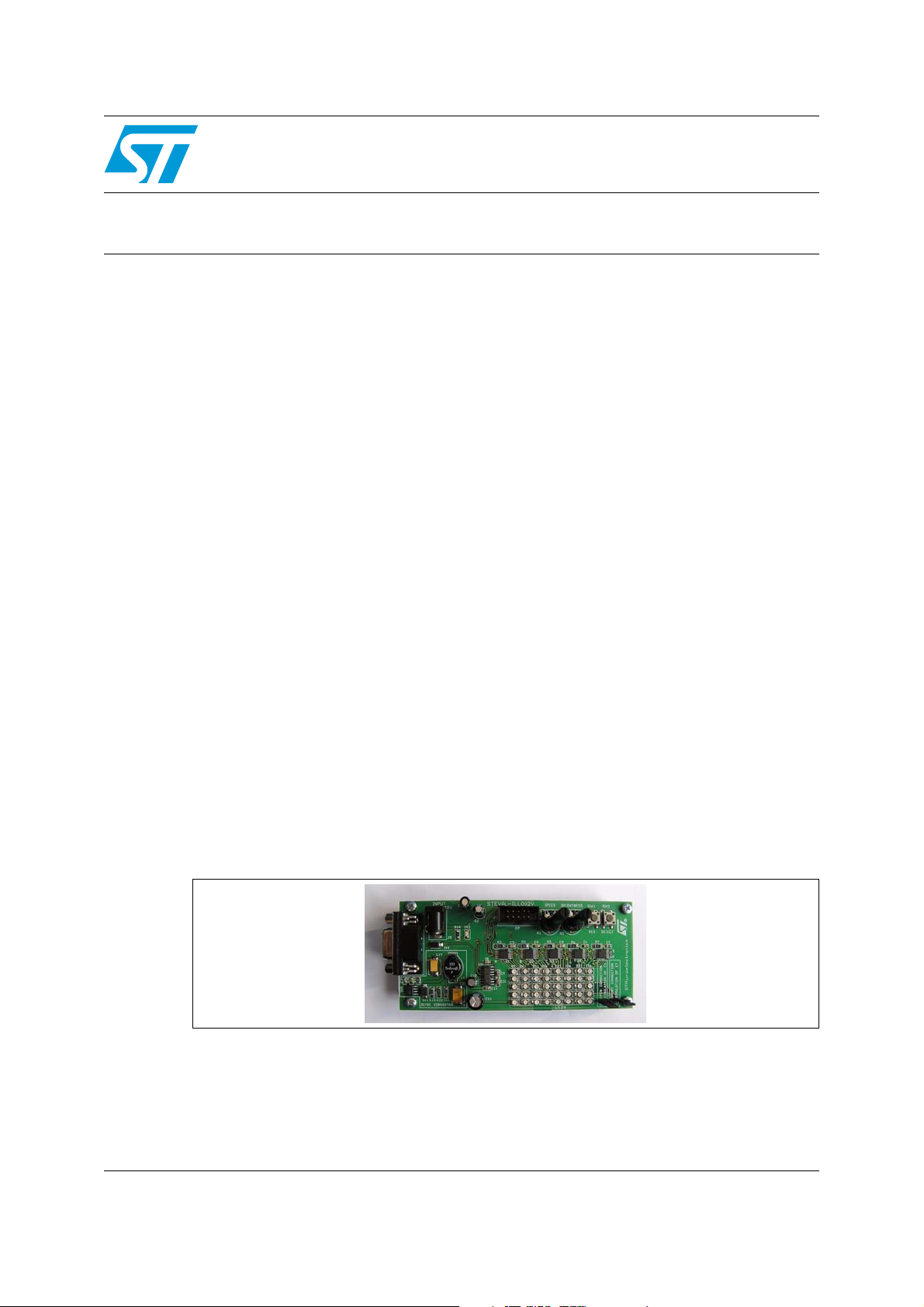
■ STEVAL-ILL002V1 using OSRAM LEDs
■ STEVAL-ILL002V2 using Toshiba LEDs
Note: The STP08CDC596 LED driver is replaced by the new, higher performing STP08DP05 LED
driver. The two available versions of the evaluation board with the STP08DP05 replace the
STEVAL-ILL002V1 and the STEVAL-ILL002V2, and are described in application note
AN2478.
The new boards available are:
■ STEVAL-ILL002V3 using OSRAM LEDs
■ STEVAL-ILL002V4 using VISHAY LEDs
Forty high-brightness LEDs are arranged on the board in a 5x8 matrix. The matrix is driven
by five 8-channel STP08CDC596 drivers.
The main features of the evaluation board are:
■ Brightness and blinking regulation
■ Animated text
■ Error detection on output
■ GUI (graphic user interface)
■ DC-DC converter
The innovative feature of the STP08CDC596 is the full output error detection function which
enables output status checking without invasive testing (via software only).
Figure 1. STEVAL-ILL002Vx evaluation board
For more information about other boards based on the STPxxC/L596 driver family, refer to
application note AN2141 which provides details concerning the basic features of the driver
family, the microcontroller interface and chip power dissipation. Refer to user manual
UM0181 for information about how to get started using the evaluation boards.
August 2007 Rev 4 1/11
www.st.com
Page 2

Contents AN2415
Contents
1 Overview . . . . . . . . . . . . . . . . . . . . . . . . . . . . . . . . . . . . . . . . . . . . . . . . . . 4
2 Operation mode switching . . . . . . . . . . . . . . . . . . . . . . . . . . . . . . . . . . . . 5
2.1 Normal mode . . . . . . . . . . . . . . . . . . . . . . . . . . . . . . . . . . . . . . . . . . . . . . . 5
2.2 Error detection mode . . . . . . . . . . . . . . . . . . . . . . . . . . . . . . . . . . . . . . . . . 6
3 Firmware implementation . . . . . . . . . . . . . . . . . . . . . . . . . . . . . . . . . . . . . 6
3.1 Timing diagram . . . . . . . . . . . . . . . . . . . . . . . . . . . . . . . . . . . . . . . . . . . . . . 6
3.2 Option byte . . . . . . . . . . . . . . . . . . . . . . . . . . . . . . . . . . . . . . . . . . . . . . . . . 7
3.3 GUI features . . . . . . . . . . . . . . . . . . . . . . . . . . . . . . . . . . . . . . . . . . . . . . . . 7
4 Revision history . . . . . . . . . . . . . . . . . . . . . . . . . . . . . . . . . . . . . . . . . . . 10
2/11
Page 3

AN2415 List of figures
List of figures
Figure 1. STEVAL-ILL002Vx evaluation board . . . . . . . . . . . . . . . . . . . . . . . . . . . . . . . . . . . . . . . . . . 1
Figure 2. STEVAL-ILL002Vx evaluation board block diagram . . . . . . . . . . . . . . . . . . . . . . . . . . . . . . 4
Figure 3. Error Detection mode . . . . . . . . . . . . . . . . . . . . . . . . . . . . . . . . . . . . . . . . . . . . . . . . . . . . . . 5
Figure 4. Normal mode . . . . . . . . . . . . . . . . . . . . . . . . . . . . . . . . . . . . . . . . . . . . . . . . . . . . . . . . . . . . 5
Figure 5. Timing diagram . . . . . . . . . . . . . . . . . . . . . . . . . . . . . . . . . . . . . . . . . . . . . . . . . . . . . . . . . . . 7
Figure 6. MCU option bytes . . . . . . . . . . . . . . . . . . . . . . . . . . . . . . . . . . . . . . . . . . . . . . . . . . . . . . . . . 7
Figure 7. LED matrix board application diagram . . . . . . . . . . . . . . . . . . . . . . . . . . . . . . . . . . . . . . . . . 8
3/11
Page 4
Overview AN2415
S
1 Overview
The STEVAL-ILL002Vx evaluation board can be powered with voltages from 7 V up to 32 V.
The SMPS DC-DC converter block is based on the L5970D step-down switching regulator
and the DC-DC block is based on the LE50ABD voltage regulator. The power topology
makes it possible to power the board using a laptop power supply.
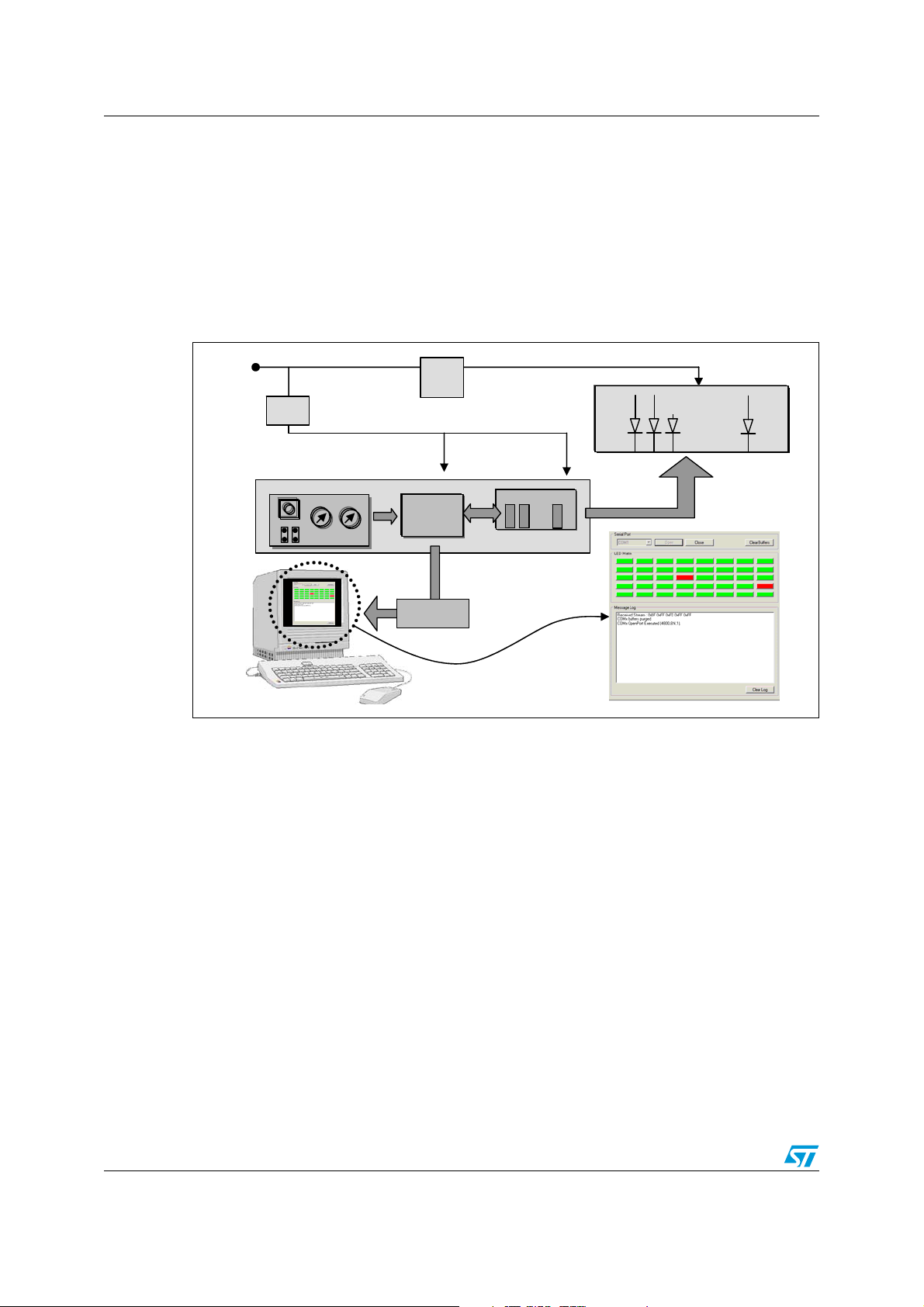
Figure 2 shows the block diagram of the evaluation board.
Figure 2. STEVAL-ILL002Vx evaluation board block diagram
SMP
Power Supply
DC/DC
DC/DC
LED M atrix
……
Control Panel
8-bit µC
RS232 Driver
LED Driver
SPI
SPI
…….
The brain of the board is the 8-bit ST7FLITE39 microcontroller. It receives inputs from the
control panel, sends and receives data from the LED drivers through the serial peripheral
interface (SPI) and enables PC communication through the serial communications interface
(SCI). The control panel consists of switches, potentiometers and jumpers. Switches are
used to reset the microcontroller and to enter Detection mode. Potentiometers change the
brightness and text speed. Jumpers are used to simulate errors (open and short circuit) on
the LED matrix.
A LED matrix consists of 40 LEDs arranged in a 5x8 matrix. A dedicated PC GUI displays
the status of the LEDS.
4/11
Page 5

AN2415 Operation mode switching
2 Operation mode switching
To enter Error Detection or Normal mode, the drivers must receive a particular sequence on
the OE and LE pins.
When a one-clock-wide short pulse “101” is sent on the OE pin, the drivers enter the
switching phase. If the LE pin is sampled as high voltage at the 4th rising edge of CLK, the
drivers switch to Error Detection mode (Figure 3). Otherwise, they switch to Normal mode
(Figure 4).
Note: In the firmware, with SW2 pressure only the drivers enter Error Detection mode, and after an
error detection check, they re-enter Normal mode.
Figure 3. Error Detection mode
Figure 4. Normal mode
2.1 Normal mode
In Normal mode, the serial data is transferred from the microcontroller to the drivers via the
SPI. The serial data from microcontroller is sent to the drivers via the SDI pin, undergoes a
shift in the Shift Register, and exits via the SDO pin. The LE pin can latch the serial data in
the Shift Register to the output latch. The OE pin enables the output driver sink current.
Current is modulated by the potentiometer, which changes the PWM duty cycle on the OE
pin (PWM frequency is set at 244 Hz).
5/11
Page 6

Firmware implementation AN2415
Note: At start-up, the evaluation board works in Normal mode.
2.2 Error detection mode
After entering Error Detection mode as shown in Figure 3, it is recommended to send all
data to the drivers as “1”.
As long as the OE pin is high, the serial data can still be shifted to the Shift Register via the
SDI pin, and out via the SDO pin. The LE pin can also send the data in the Shift Register to
the output latch.
When the state of the OE pin is pulled down to low voltage for at least 2 µs, the drivers
execute the error detection function and load the error status into the Shift Register. The
error status codes saved in the Shift Register can then be shifted out via the SDO pin bit-bybit along with the clock. The SDO pin of the last driver of the chain is connected to the MISO
pin of the microcontroller. Incoming data can be sent to the PC through the SCI and
displayed on the GUI. For more information, refer to the timing diagram shown in Figure 5.
3 Firmware implementation
The purpose of this application note is to explain how to manage the error detection features
of the drivers. Refer to AN2141 for an explanation of the basic driver features.
3.1 Timing diagram
At power-up, the microcontroller sends data to the drivers’ Shift Register via the SPI
configured at 250 kHz. The maximum communication frequency for this driver is 25 MHz to
satisfy high volume data transmissions. (Please refer to the device datasheet for more
details). The two potentiometers are connected to ADC inputs. The analog voltage inputs
are converted to a digital value. According to this digital value, it will change the PWM
duty-cycle signal for brightness and data time delay for text speed. By default, the
microcontroller works in Normal mode and only enters Error Detection mode when an
external interrupt pin connected to SW2 is triggered. The related ISR disables the SPI I/O
function and sends a specific sequence to the driver via the CLK, OE, and LE pins as shown
in Figure 5.
After the driver has received the specific sequence, the microcontroller enables the SPI and
sends 0xFF data for each driver. The drivers have already entered Error Detection mode
and the microcontroller maintains pin OE low for detecting the error status. Drivers send
back the LED status to the microcontroller via the MISO pin (connected to the SDO pin).
Then, the microcontroller resumes Normal mode operation, sending the specific sequence
to the drivers. Figure 5 shows each phase, switching from Error Detection to Normal modes.
6/11
Page 7
AN2415 Firmware implementation
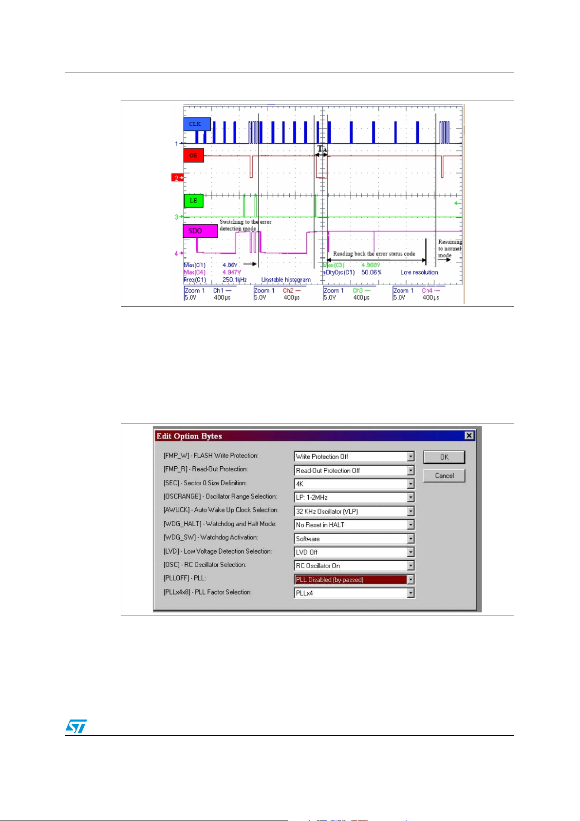
Figure 5. Timing diagram
Note: T
Note: The SDO of the E driver is connected to the MISO pin of the MCU.
must be at least 2 µs to detect the error status.
A
3.2 Option byte
Figure 6 shows the option byte settings.
Figure 6. MCU option bytes
3.3 GUI features
A dedicated graphical user interface (GUI) displays the LEDs, status on the PC. The serial
parameters are: 4800, 8, N, 1 (baud rate, 8 bit, parity none, 1 bit stop). The microcontroller,
7/11
Page 8
Application diagram AN2415
after resuming Normal mode, manages the SCI peripheral and sends data to the PC using
the ST232ABN driver interface.
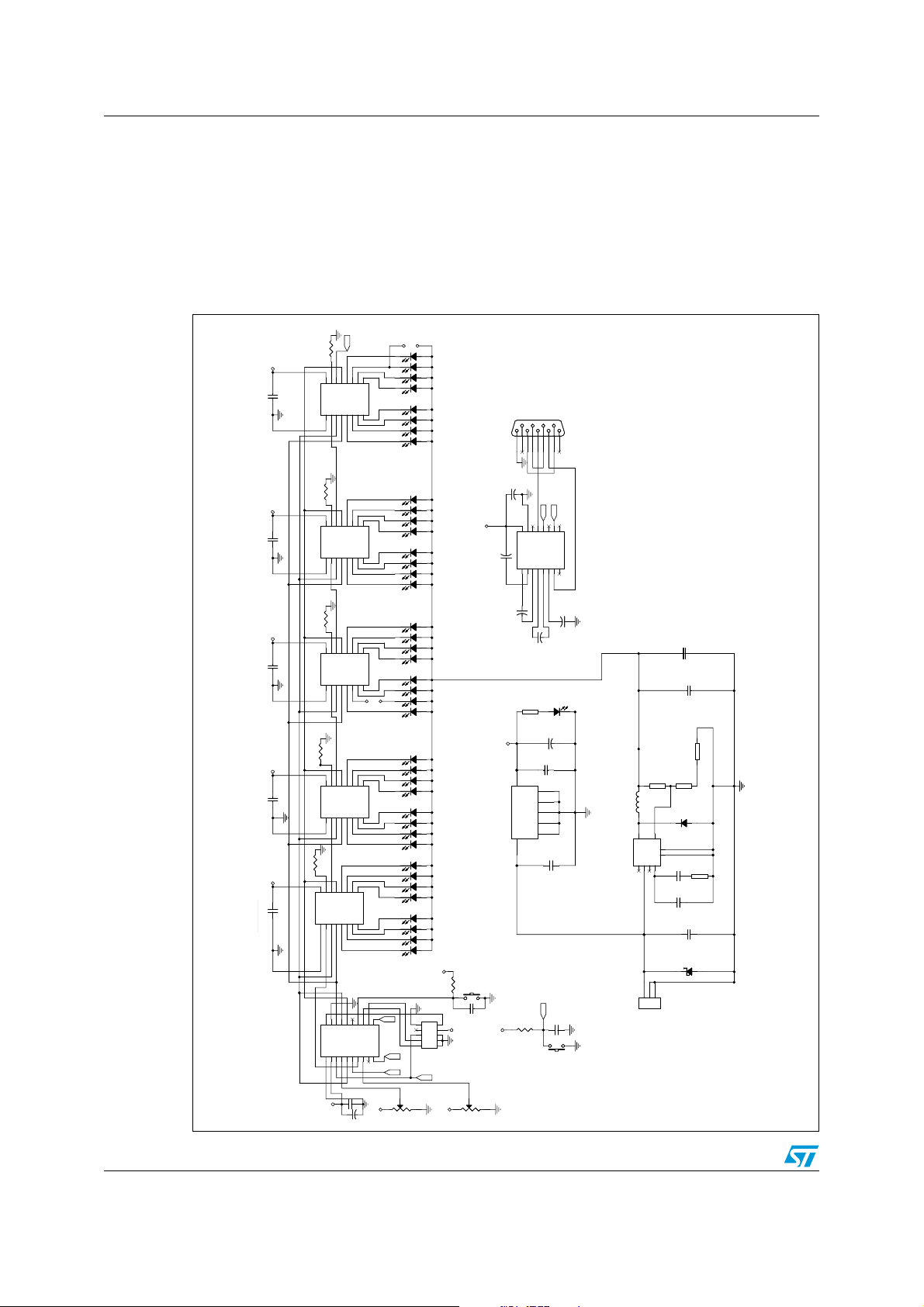
Appendix A Application diagram
Figure 7. LED matrix board application diagram
JP1
JP1
SD0
R7 1k3R7 1k3
13
16
10
14
9
15
9
1212111110
/OE
Vdd
C7
100nFC7100nF
C6
100nFC6100nF
R-EXT
GND1SDI2CLK3/LE45566778
U5
R6
1k3R61k3
16
15
Vdd
R-EXT
GND1SDI2CLK3/LE45566778
U4
SDO
STP08CDC596/EU5STP08CDC596/E
8
13
10
14
9
9
1212111110
/OE
SDO
STP08CDC596/DU4STP08CDC596/D
8
1 2
JUMPER
JUMPER
P1
VCC
C12
C12
470nF
470nF
C11
C11
594837261
2.2uF
2.2uF
16
RDI
TxD
15
13
12
14
Vdd
T1IN11T2IN
GND
R1IN
T1OUT
R1OUT
C1+1V+2C1-3C2+4C2-5V-6T2OUT7R2IN
CONNECTOR DB9P1CONNECTOR DB9
STEVAL-ILL002V1 (OSRAM LEDs)
STEVAL-ILL002V2 (TOSHIBA LEDs)
RxD
TDO
10
9
R2OUT
U6 ST232ABNU6 ST232ABN
8
<Doc> <RevCode>
DiagnosticLED Driver
<Doc> <RevCode>
DiagnosticLED Driver
<Doc> <RevCode>
DiagnosticLED Driver
B
B
B
Title
Size DocumentNumber Rev
Title
Size DocumentNumber Rev
Title
Size DocumentNumber Rev
470nF
470nF
C10
1k3R51k3
100nFC5100nF
100nFC4100nF
100nFC3100nF
R5
16
15
Vdd
R-EXT
U3
GND1SDI2CLK3/LE45566778
R4
1K3R41K3
15
16
Vdd
R-EXT
GND1SDI2CLK3/LE45566778
U2
R3
1k3R31k3
16
14
15
Vdd
SDO
R-EXT
GND1SDI2CLK3/LE45566778
U1
201918171615141312
U8
123456789
VCC
13
14
10
9
9
1212111110
/OE
SDO
STP08CDC596/CU3STP08CDC596/C
8
D18D18
1 2
JP2
JP2
JUMPER
JUMPER
10
13
9
14
9
1212111110
/OE
SDO
STP08CDC596/BU2STP08CDC596/B
8
13
10
9
9
1212111110
/OE
STP08CDC596/AU1STP08CDC596/A
8
D1 D20 D28D25D8 D12 D40D4 D9 D30D27D24D5 D7 D26 D29D6 D33D10 D34D2 D21 D37D16 D36D3 D39D17 D35D15 D32D23 D38D13D11 D14 D22D19 D31
VCC
R8
10kR810k
J1ICP J1ICP
9
10
7
8
TDO
11
ST7lite3U8ST7lite3
10
C13
10nF
C13
10nF
13
+
+
VCC
C2
C2
0uF
0uF
5
6
VCC
3
4
1
2
SD0 RDI
RES
2
R2
10kR210k
R1
13
VCC
VCC VCCVCC VCCVCC
C5
C4
C3
C10
VCC
1
VOUT
VIN
U7 LE50/SOU7 LE50/SO
8
SW2SW2
C14
C14
2
R9
10nF
10nF
VCC
10kR110k
R14
R14
10kR910k
INHIB
GND
GND
GND
GND
470nFC8470nF
C8
220uF/25V
220uF/25V
C21
C21
+
21
L1 33uHL1 33uH
1
682
123
J5 CON3J5 CON3
INPUT VOLTAGE
R11
R11
5
7
3
4
FROM 7V UP TO 32V
+
C22
C22
100uF/16V
100uF/16V
R13
360
R13
360
6k8
6k8
R12
2K2
R12
2K2
D41
D41
STPS340U
STPS340U
C18
22nF
C18
22nF
R10
4k7
R10
4k7
C20
C20
220pF
220pF
C19
C19
10uF/35V
10uF/35V
D44
SMAJ33A-TR
D44
SMAJ33A-TR
C9
470nFC9470nF
D42
D42
560
560
GREEN L ED
GREEN L ED
C1
2.2uFC12.2uF
C15
C15
100nF
100nF
5
7
6
3
2
C17
100nF
C17
100nF
IO5 L5970DIO5 L5970D
RES
C16
10nF
C16
10nF
SW1SW1
8/11
Page 9

AN2415 Bill of materials
Appendix B Bill of materials
Table 1. Bill of materials
Item Qty Reference Part Description Order code Supplier
1 2 C1 and C12 2.2 µF/50 V Electrolytic capacitor
2 1 C2 10 µF/35 V Electrolytic capacitor
37
44
5a 2 C14 and C16 10 nF/50 V
5b 1 C13 10 nF/50 V
6 1 C18 22 nF/50 V
7 1 C19 10 µF/35 V Tantal capacitor
8 1 C20 220 pF/50 V
9 1 C21 220 µF/25 V Electrolytic capacitor
10 1 C22 100 µF/16 V Tantal capacitor
11 40
C3, C4, C5, C6,
C7, C15 and
C17
C8, C9, C10
and C11
D1, D2, D3, D4,
D5, D6, D7, D8,
D9, D10, D11,
D12, D13, D14,
D15, D16, D17,
D18, D19, D20,
D21, D22, D23,
D24, D25, D26,
D27, D28, D29,
D30, D31, D32,
D33, D34, D35,
D36, D37, D38,
D39 and D40
100 nF/50 V
470 nF/16 V
LED
Ceramic capacitor
SMD 0805
Ceramic capacitor
SMD 0805
Ceramic capacitor
SMD 0805
Ceramic capacitor
SMD 1206
Ceramic capacitor
SMD 0805
Ceramic capacitor
SMD 0805
OSRAM SMD BLUE
LED LB T68C-P2S1-35
or TOSHIBA
LED - TLGE1100
OSRAM or
TOSHIBA
12 1 D41 STPS340U Diode STPS340U STMicroelectronics
13 1 D42 GREEN LED SMD LED 1206
14 1 D44 SMAJ33A-TR Transil SMAJ33A-TR STMicroelectronics
15 1 IO5 L5970D DC-DC converter L5970D STMicroelectronics
16 2 JP1 and JP2 JUMPER Jumpers + switches
17 1 J1 ICP Programming connector
18 1 J5 CON3 Input connector
9/11
Page 10

Revision history AN2415
Table 1. Bill of materials (continued)
Item Qty Reference Part Description Order code Supplier
19 1 L1 33 µH Inductor DO3316P-333ML Coilcraft
20 1 P1
21a 2 R1 and R2 10 k
21b 2 R8 and R9 10 k SMD resistors 0805
22 5
23 1 R10 4k7 SMD resistors 0805
24 1 R11 6k8 SMD resistors 1206
25 1 R12 2K2 SMD resistors 1206
26 1 R13 360 SMD resistors 1206
27 1 R14 560 SMD resistors 1206
28 2 SW1 and SW2
29 5
30 1 U6 ST232ABD RS232 driver ST232ABD STMicroelectronics
31 1 U7 LE50/SO Linear voltage regulator LE50ABD STMicroelectronics
32 1 U8 ST7lite3 Microcontroller ST7FLITE39F2M6 STMicroelectronics
R3, R4, R5, R6
and R7
U1, U2, U3, U4
and U5
CONNECTOR
DB9
1k3 SMD resistors 1206
Push-button
switch
STP08CDC596 LED drivers STP08CDC596TTR STMicroelectronics
CAN connector - 9 pin
Potentiometers with
axis
Switch
4 Revision history
Table 2. Revision history
Date Revision Changes
7-Sept-2006 1 Initial release.
31-Jan-2007 2
08-Feb-2007 3 Bill of materials table modified.
30-Aug-2007 4 Minor text changes
10/11
Bill of materials table and LED matrix board application diagram
modified.
Page 11

AN2415
Please Read Carefully:
Information in this document is provided solely in connection with ST products. STMicroelectronics NV and its subsidiaries (“ST”) reserve the
right to make changes, corrections, modifications or improvements, to this document, and the products and services described herein at any
time, without notice.
All ST products are sold pursuant to ST’s terms and conditions of sale.
Purchasers are solely responsible for the choice, selection and use of the ST products and services described herein, and ST assumes no
liability whatsoever relating to the choice, selection or use of the ST products and services described herein.
No license, express or implied, by estoppel or otherwise, to any intellectual property rights is granted under this document. If any part of this
document refers to any third party products or services it shall not be deemed a license grant by ST for the use of such third party products
or services, or any intellectual property contained therein or considered as a warranty covering the use in any manner whatsoever of such
third party products or services or any intellectual property contained therein.
UNLESS OTHERWISE SET FORTH IN ST’S TERMS AND CONDITIONS OF SALE ST DISCLAIMS ANY EXPRESS OR IMPLIED
WARRANTY WITH RESPECT TO THE USE AND/OR SALE OF ST PRODUCTS INCLUDING WITHOUT LIMITATION IMPLIED
WARRANTIES OF MERCHANTABILITY, FITNESS FOR A PARTICULAR PURPOSE (AND THEIR EQUIVALENTS UNDER THE LAWS
OF ANY JURISDICTION), OR INFRINGEMENT OF ANY PATENT, COPYRIGHT OR OTHER INTELLECTUAL PROPERTY RIGHT.
UNLESS EXPRESSLY APPROVED IN WRITING BY AN AUTHORIZED ST REPRESENTATIVE, ST PRODUCTS ARE NOT
RECOMMENDED, AUTHORIZED OR WARRANTED FOR USE IN MILITARY, AIR CRAFT, SPACE, LIFE SAVING, OR LIFE SUSTAINING
APPLICATIONS, NOR IN PRODUCTS OR SYSTEMS WHERE FAILURE OR MALFUNCTION MAY RESULT IN PERSONAL INJURY,
DEATH, OR SEVERE PROPERTY OR ENVIRONMENTAL DAMAGE. ST PRODUCTS WHICH ARE NOT SPECIFIED AS "AUTOMOTIVE
GRADE" MAY ONLY BE USED IN AUTOMOTIVE APPLICATIONS AT USER’S OWN RISK.
Resale of ST products with provisions different from the statements and/or technical features set forth in this document shall immediately void
any warranty granted by ST for the ST product or service described herein and shall not create or extend in any manner whatsoever, any
liability of ST.
ST and the ST logo are trademarks or registered trademarks of ST in various countries.
Information in this document supersedes and replaces all information previously supplied.
The ST logo is a registered trademark of STMicroelectronics. All other names are the property of their respective owners.
© 2007 STMicroelectronics - All rights reserved
STMicroelectronics group of companies
Australia - Belgium - Brazil - Canada - China - Czech Republic - Finland - France - Germany - Hong Kong - India - Israel - Italy - Japan -
Malaysia - Malta - Morocco - Singapore - Spain - Sweden - Switzerland - United Kingdom - United States of America
www.st.com
11/11
 Loading...