

AN2407
Application note
800mA standalone linear Li-Ion
battery charger with thermal regulation
Introduction
One way to minimize the size and complexity of a battery charger is to use a linear-type
charger. The linear charger drops the AC adapter voltage down to the battery voltage. The
number of external components is low: linear chargers require input and output bypass
capacitors, and sometimes need an external pass transistor, and resistors for setting voltage
and current limits.
The main pitfall of a linear charger is power dissipation. The charger simply drops the AC
adapter voltage down to the battery voltage.
In the case of an 800mA charger, a 5V±10% regulated AC adapter voltage, and battery
voltage that varies between 4.2V and 2.5V, the power dissipation can range from 0.6W to
2.0W.
This type of charger is simpler than the switch-mode type, mainly because the passive LC
filter is not required. It dissipates the most power when the battery voltage is at its minimum,
since the difference between the fixed input voltage and the battery voltage is greatest
during this condition.
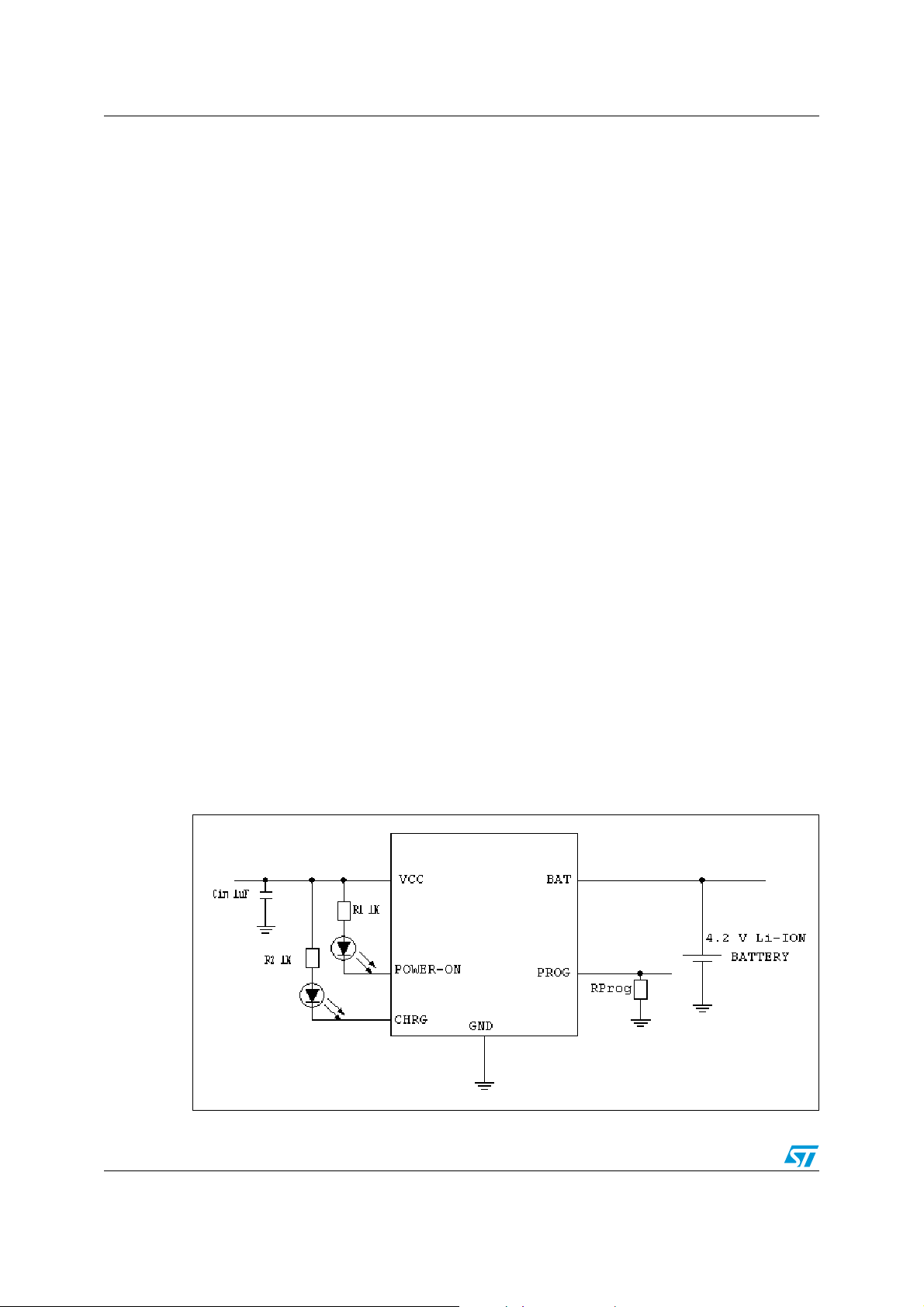
Application diagram
September 2006 Rev 2 1/14
www.st.com

Contents AN2407
Contents
1 STBC08 description . . . . . . . . . . . . . . . . . . . . . . . . . . . . . . . . . . . . . . . . . 3
2 Stability considerations . . . . . . . . . . . . . . . . . . . . . . . . . . . . . . . . . . . . . . 4
3 Board layout considerations . . . . . . . . . . . . . . . . . . . . . . . . . . . . . . . . . . 5
4 External components . . . . . . . . . . . . . . . . . . . . . . . . . . . . . . . . . . . . . . . . 6
5 Power dissipation . . . . . . . . . . . . . . . . . . . . . . . . . . . . . . . . . . . . . . . . . . . 7
6 Automatic recharge . . . . . . . . . . . . . . . . . . . . . . . . . . . . . . . . . . . . . . . . . . 8
7 CHRG and Power-on status output pins . . . . . . . . . . . . . . . . . . . . . . . . . 9
8 USB and wall adapter power . . . . . . . . . . . . . . . . . . . . . . . . . . . . . . . . . 10
9 Charge current . . . . . . . . . . . . . . . . . . . . . . . . . . . . . . . . . . . . . . . . . . . . . 11
9.1 Programming charge current . . . . . . . . . . . . . . . . . . . . . . . . . . . . . . . . . . 11
9.2 Maximum charge current in temperature . . . . . . . . . . . . . . . . . . . . . . . . . 11
Appendix A Board layout . . . . . . . . . . . . . . . . . . . . . . . . . . . . . . . . . . . . . . . . . . . . 12
Revision history . . . . . . . . . . . . . . . . . . . . . . . . . . . . . . . . . . . . . . . . . . . . . . . . . . . . 13
2/14
AN2407 STBC08 description
1 STBC08 description
The STBC08 is a constant current/constant voltage charger for single cell Li-Ion battery. No
external sense resistor or blocking diode is required and its MLPD 3x3mm² 6L package
make it ideally suited for portable applications.
The STBC08 is designed to comply with USB power specifications. An internal block
regulates the current when the junction temperature increases in order to protect the device
when it operates in high power or high ambient temperature.
The maximum power dissipation occurs when V
current.
The charge voltage is fixed at 4.2V, and the charge current limitation can be programmed
using a single resistor connected between pins PROG and GND. The charge cycle finishes
when the current flowing to the battery is 1/10 of the programmed value. If the external
adaptor is removed, the STBC08 switches off and only 2µA can flow from the battery to the
device. The device can be put into Shutdown Mode, reducing the supply current to 25µA.
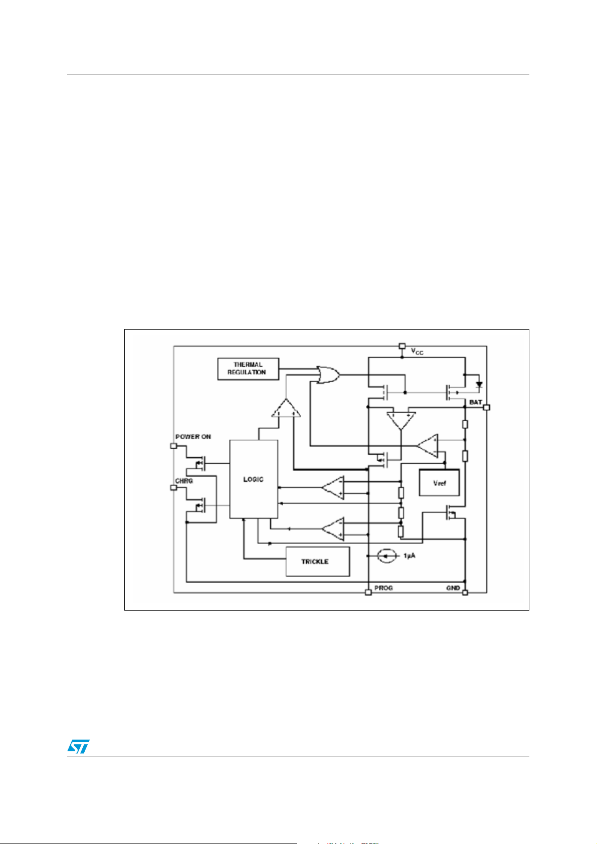
Figure 1. Block diagram
is 2.9V with the maximum charge
BAT
3/14
Stability considerations AN2407
2 Stability considerations
The STBC08 contains two control loops: constant voltage and constant current. The
constant-voltage loop is stable without any compensation when a battery is connected with
low impedance leads. Excessive lead length, however, may add enough series inductance
to require a bypass capacitor of at least 1µF from BAT to GND. Furthermore, a 4.7µF
capacitor with a 0.2Ω to 1Ω series resistor from BAT to GND is required to keep ripple
voltage low when the battery is removed.
High value capacitors with very low ESR (especially ceramic) reduce the constant-voltage
loop phase margin.
Ceramic capacitors up to 22µF may be used in parallel with a battery, but larger ceramics
should be decoupled with 0.2Ω to 1Ω of series resistance.
In constant-current mode, the PROG pin is in the feedback loop, not the battery. Because of
the additional pole created by PROG pin capacitance, capacitance on this pin must be kept
to a minimum. With no additional capacitance on the PROG pin, the charger is stable with
program resistor values as high as 12k. However, additional capacitance on this node
reduces the maximum allowed program resistor.Therefore, if the PROG pin is loaded with a
capacitance, C
resistance value for R
, the following equation should be used to calculate the maximum
PROG
PROG
:
Equation 1
R
PROG
----------------------------------------------------------
≤
2π 510•
1
5
C
••
PROG
Average, rather than instantaneous, battery current may be of interest to the user. For
example, if a switching power supply operating in low current mode is connected in parallel
with the battery, the average current being pulled out of the BAT pin is typically of more
interest than the instantaneous current pulses. In such a case, a simple RC filter can be
used on the PROG pin to measure the average battery current as shown in Figure 2.
This design includes a 20kΩ resistor between the PROG pin and the filter capacitor to
ensure stability (C
FILTER
= 100nF).
Figure 2. Isolating capacitive load on PROG pin and filtering
4/14
AN2407 Board layout considerations
3 Board layout considerations
Due to the small size of the MLP package, it is very important to use a good thermal PC
board layout to maximize the available charge current. The thermal path for the heat
generated by the IC is from the die to the copper lead frame, through the package leads,
(especially the ground lead) to the PC board copper. The PC board copper is the heat sink.
The footprint copper pads should be as wide as possible and expand out to larger copper
areas to spread and dissipate the heat to the surrounding ambient. Feed-through vias to
inner or backside copper layers are also useful in improving the overall thermal performance
of the charger. Other heat sources on the board, not related to the charger, must also be
considered when designing a PC board layout because they will affect overall temperature
rise and the maximum charge current.
Ta bl e 1 lists thermal resistance for several different board sizes and copper areas.
Table 1. Measured thermal resistance (2-layer board)
Copper area
Top Bottom
50mm
2
2
2
2
2
2500mm
2500mm
2500mm
2500mm
2500mm
2500mm
1000mm
225mm
100mm
Board area
2
2
2
2
2
2500mm
2500mm
2500mm
2500mm
2500mm
2
2
2
2
2
Thermal resistance
junction-to-ambient
125°C/W
125°C/W
130°C/W
135°C/W
150°C/W
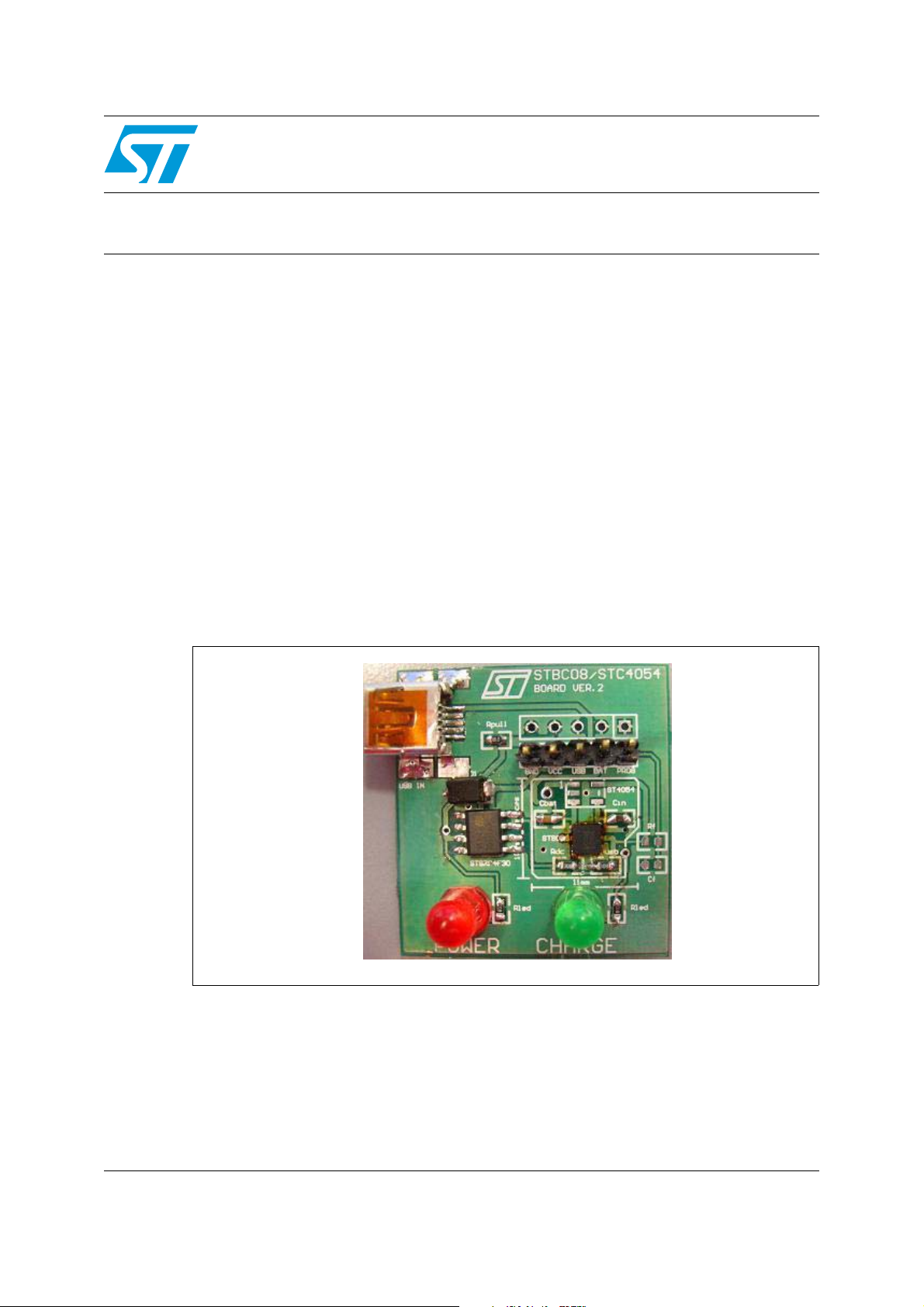
Appendix A: Board layout on page 12 contains an illustration of the complete assembly
board.
5/14
External components AN2407
4 External components
This application requires few external components: two ceramic capacitors (CIN = 1µF,
C
= 4.7µF) and one resistor (R
OUT
For input and output capacitors, ST recommends using ceramic capacitors with low ESR.
For good stability of device supplied from low input voltage 2.6V at maximum ratings of
output, ST recommends using 1µF/6.3V as a minimum value for the input capacitor and
4.7µF/6.3V as a minimum value for the output capacitor.
Table 2. Bill of materials
Symbol Parameter Type Qty Supplier Value Unit
PROG
).
Cin Input Cap.
Cbat Output Cap.
Rusb Usb Current Set Thick film type 1% CRG0603J2K0 1 THCO 2 KOhm
Rdc DC Current Set Thick film type 1% CRG0603J10K0 1 THCO 10 KOhm
N-Pmos Nmos-Pmos IC STS7C4F30 1 ST
D1 SCHOTTKY STPS1L40M 1 ST
Rled Limit Led Current Thick film type 1% CRG0603J1K0 2 THCO 1 KOhm
Rpull Pull down resistor Thick film type 1% CRG0603J1K0 1 THCO 1 KOhm
Rf Resistance Filter Thick film type 1% CRG0603J20K0 1 THCO 20 KOhm
Cf Capacitor Filter
Led Power Led
Led Charge Led 1.8mm-GREEN LED L-2060GD 1 KINGBRIGHT
USB In Connector USB
Ceramic Low ESR
GRM155F50J105ZE01
Ceramic Low ESR
GRM188r60J475ke19
Ceramic Low ESR
GRM188r71e104ka01
1.8mm-RED LED
L-2060ID
Mini B
54819-0572
1 Murata 1 µF
1 Murata 4.7 µF
1 Murata 100 nF
1 KINGBRIGHT
1Molex
6/14

AN2407 Power dissipation
5 Power dissipation
The conditions that cause the STBC08 to reduce charge current through thermal feedback
can be approximated by considering the power dissipated in the IC. For high charge
currents, the STBC08 power dissipation is approximately:
Equation 2
P
VCCV
D
–()I
BAT
•=
BAT
where P
voltage and I
is the power dissipated, VCC is the input supply voltage, V
D
is the current charge current. It is not necessary to perform any worst-case
BAT
is the battery
BAT
power dissipation scenarios because the STBC08 will automatically reduce the charge
current to maintain the die temperature at approximately 120° C.
However, the approximate ambient temperature at which the thermal feedback begins to
protect the IC is:
Equation 3
T
120° CPDθ
A
–=
JA
Equation 4
120° CVCCV
T
A
–=
–()I
•θ
BAT
BAT
JA
Example: Consider an STBC08 operating from a 5V wall adapter providing 400mA to a 3.7V
Li-Ion battery. The ambient temperature above which the STBC08 will begin to reduce the
400mA charge current is approximately:
Equation 5
C
120° C5V3.7V–()400m A()• 105°
T
A
-----
• 42° C=–=
W
The STBC08 can be used above 42°C, but the charge current will be reduced from 400mA.
The approximate current at a given ambient temperature can be calculated:
Equation 6
120° CTA–
------------------------------------------------- -=
I
BAT
V
–()θ
CCVBAT
•
A
Using the previous example with an ambient temperature of 65°C, the charge current will be
reduced to approximately:
Equation 7
120° C65° C–
---------------------------------------------------------
I
BAT
5V 3.7V–()150°
•
282m A==
C
-----
W
Furthermore, the voltage at the PROG pin will change proportionally with the charge current
as discussed in Section 9.1: Programming charge current. It is important to remember that
STBC08 applications do not need to be designed for worst-case thermal conditions since
the IC will automatically reduce power dissipation when the junction temperature reaches
approximately 120°C.
7/14

Automatic recharge AN2407
6 Automatic recharge
Once the charge cycle is terminated, the STBC08 continuously monitors the voltage on the
BAT pin using a comparator with a 2-ms filter time (t
RECHARGE
when the battery voltage falls below 4.05V (which corresponds to approximately 80% to
90% battery capacity).
This ensures that the battery is kept at or near a fully-charged condition and eliminates the
need for periodic charge cycle initiations. The CHRG output enters a strong pulldown state
during recharge cycles.
Figure 3. State diagram of a typical charge cycle
). A charge cycle restarts
POWER ON
RECONNECTED
CONDITION
PROG
OR
UVLO
STOPS
SHUTDOWN MODE
CHRG: Hi-Z IN UVLO
PULL-DOWN
OTHERWISE
ICC DROPS TO <25µA
PROG FLOATED
OR
UVLO
CONDITION
Bat <2.9V
TRICKLE CHARGE
MODE
1/10TH FULL
CURRENT
CHRG: PULL-DOWN
Bat >2.9V
CHARGE MODE
FULL CURRENT
CHRG: PULL-DOWN
STANDBY MODE
NO CHARGE
CURRENT
CHRG: HI-Z
PULL-DOWN
Bat >2.9V
Prog<100mV
2.9V<Vbat<4.05V
8/14
AN2407 CHRG and Power-on status output pins
7 CHRG and Power-on status output pins
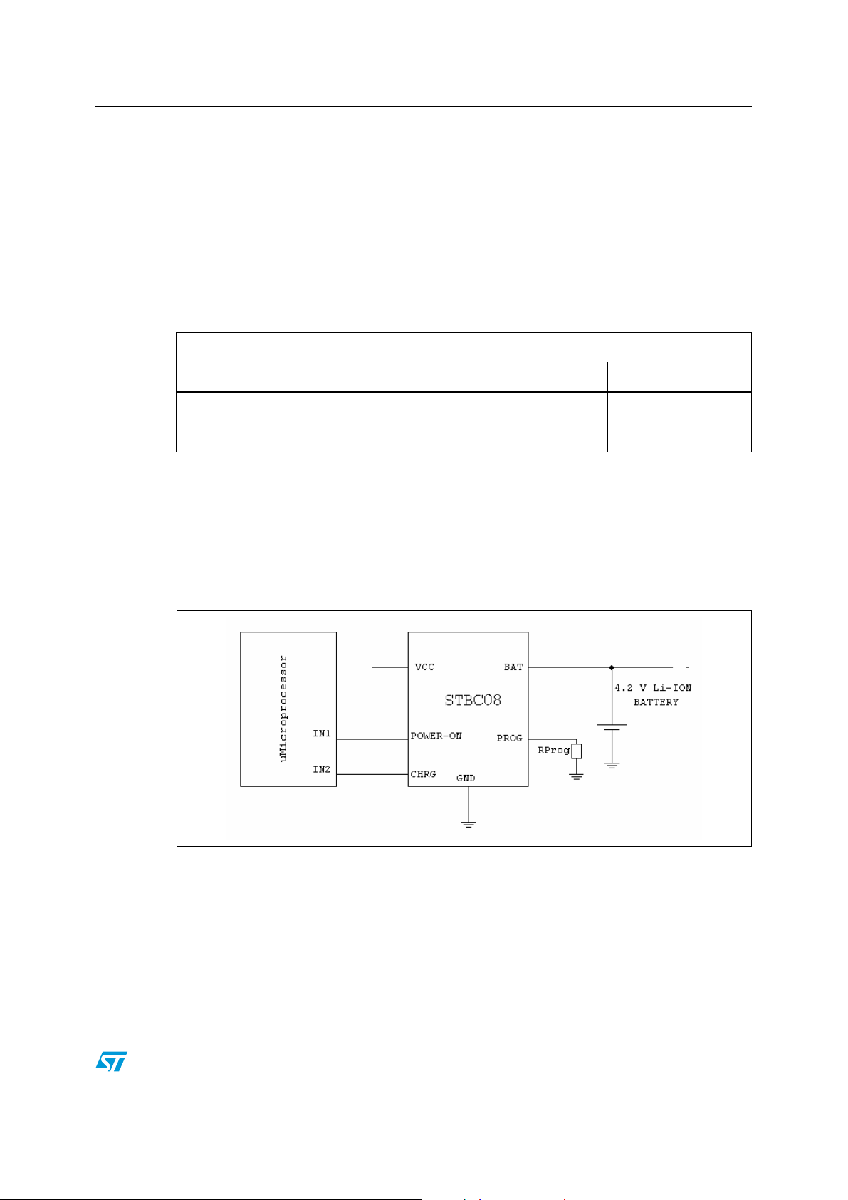
The POWER ON pin (open drain) is a flag that indicates the presence of the VCC,
V
UVLO<VCC
V
CC<VBAT
The CHRG pin (open drain) is a flag that indicates the status of the charge, if the pin is low
the device works and the charge is going, when the pin is high impedance the charge is
finished (constant Voltage and I
Table 3. LEDs status
The values in Ta bl e 3 correspond to the following modes:
– 00 is Precharge mode (Trickle Charge mode) or Charge Mode. V
– 01 is Standby mode (completed charge) or Shutdown mode (R
– 11 is Supply (insufficient and unqualified.)
<7.2V and VCC>V
. High impedance indicates that VCC< V
BAT
. In this case VCC is insufficient.
PROG
Low 00 01
Power-ON
High Not used 11
V
UVLO
and R
is present on the PROG pin.
PROG
connected).
/10).
, VCC>7.2V or
UVLO
CHRG
Low High
is more than
CC
not
PROG
Figure 4. Using a microprocessor to determine device state
9/14

USB and wall adapter power AN2407
8 USB and wall adapter power
Although the STBC08 allows charging from a USB port, a wall adapter can also be used to
charge Li-Ion batteries.
Figure 5 shows an example of how to combine wall adapter and USB power inputs. A
P-channel MOSFET is used to prevent back conducting into the USB port when a wall
adapter is present and Schottky diode is used to prevent USB power loss through the 1kΩ
pull-down resistor. Typically, a wall adapter can supply significantly more current than the
500mA-limited USB port. Therefore, an N-channel MOSFET and an extra program resistor
are used to increase the charge current to 850mA when the wall adapter is present.
Figure 5. Combining wall adapter and USB power
10/14

AN2407 Charge current
9 Charge current
9.1 Programming charge current
The charge current is programmed using a single resistor from the PROG pin to ground.
The battery charge current is 1000 times the current out of the PROG pin. The program
resistor and the charge current are calculated using the following equations:
Equation 8
1.00V
--------------- -
R
PROG
The charge current out of the BAT pin can be determined at any time by monitoring the
PROG pin voltage using the following equation:
Equation 9
I
BAT
9.2 Maximum charge current in temperature
1000
V
PROG
------------------- -
R
PROG
•=
I
BAT
1000•=
Initial conditions: VIN = 4.4V, V
Figure 6. I
vs. temperature
BAT
The 1A battery current set by R
= 3.1V, R
BAT
is constant in the -40° to 25° C temperature range.
PROG
= 1kΩ and Air flow = 4 l/s.
PROG
For temperatures higher than 25° C, the current is lower due to the thermal limit of the
device.
11/14

Board layout AN2407
Appendix A Board layout
Figure 7. Top component demo board
Figure 8. Top layer layout Figure 9. Bottom layer layout
12/14

AN2407 Revision history
Revision history
Table 4. Document revision history
Date Revision Changes
7-Sept-2006 1 Initial release.
19-Sept-2006 2 Table 2 changed
13/14

AN2407
Please Read Carefully:
Information in this document is provided solely in connection with ST products. STMicroelectronics NV and its subsidiaries (“ST”) reserve the
right to make changes, corrections, modifications or improvements, to this document, and the products and services described herein at any
time, without notice.
All ST products are sold pursuant to ST’s terms and conditions of sale.
Purchasers are solely responsible for the choice, selection and use of the ST products and services described herein, and ST assumes no
liability whatsoever relating to the choice, selection or use of the ST products and services described herein.
No license, express or implied, by estoppel or otherwise, to any intellectual property rights is granted under this document. If any part of this
document refers to any third party products or services it shall not be deemed a license grant by ST for the use of such third party products
or services, or any intellectual property contained therein or considered as a warranty covering the use in any manner whatsoever of such
third party products or services or any intellectual property contained therein.
UNLESS OTHERWISE SET FORTH IN ST’S TERMS AND CONDITIONS OF SALE ST DISCLAIMS ANY EXPRESS OR IMPLIED
WARRANTY WITH RESPECT TO THE USE AND/OR SALE OF ST PRODUCTS INCLUDING WITHOUT LIMITATION IMPLIED
WARRANTIES OF MERCHANTABILITY, FITNESS FOR A PARTICULAR PURPOSE (AND THEIR EQUIVALENTS UNDER THE LAWS
OF ANY JURISDICTION), OR INFRINGEMENT OF ANY PATENT, COPYRIGHT OR OTHER INTELLECTUAL PROPERTY RIGHT.
UNLESS EXPRESSLY APPROVED IN WRITING BY AN AUTHORIZED ST REPRESENTATIVE, ST PRODUCTS ARE NOT
RECOMMENDED, AUTHORIZED OR WARRANTED FOR USE IN MILITARY, AIR CRAFT, SPACE, LIFE SAVING, OR LIFE SUSTAINING
APPLICATIONS, NOR IN PRODUCTS OR SYSTEMS WHERE FAILURE OR MALFUNCTION MAY RESULT IN PERSONAL INJURY,
DEATH, OR SEVERE PROPERTY OR ENVIRONMENTAL DAMAGE. ST PRODUCTS WHICH ARE NOT SPECIFIED AS "AUTOMOTIVE
GRADE" MAY ONLY BE USED IN AUTOMOTIVE APPLICATIONS AT USER’S OWN RISK.
Resale of ST products with provisions different from the statements and/or technical features set forth in this document shall immediately void
any warranty granted by ST for the ST product or service described herein and shall not create or extend in any manner whatsoever, any
liability of ST.
ST and the ST logo are trademarks or registered trademarks of ST in various countries.
Information in this document supersedes and replaces all information previously supplied.
The ST logo is a registered trademark of STMicroelectronics. All other names are the property of their respective owners.
© 2006 STMicroelectronics - All rights reserved
STMicroelectronics group of companies
Australia - Belgium - Brazil - Canada - China - Czech Republic - Finland - France - Germany - Hong Kong - India - Israel - Italy - Japan -
Malaysia - Malta - Morocco - Singapore - Spain - Sweden - Switzerland - United Kingdom - United States of America
www.st.com
14/14
 Loading...