

AN2406
Application note
TS4962IQ class D audio amplifier
Evaluation board user guidelines
Features
■ TS4962IQ low voltage class D differential audio power amplifier with standby mode
■ Operating range from Vcc=2.4V to 5.5V
■ 2.2W output power @ Vcc=5V, THD=1%, F=1kHz, with 4Ω load
■ 1.4W output power @ Vcc=5V, THD=1%, F=1kHz, with 8Ω load
■ Ultra low power consumption in standby mode (10nA)
■ 63dB PSRR @ 217Hz in grounded mode (Av=2V/V)
■ Low pop & click
■ Fast startup time: 5ms
■ Module gain set at 2V/V
Description
This mono class D demoboard is designed for the TS4962IQ class D audio amplifier. The
TS4962IQ device, in a DFN pac kage, is mounted on a t wo-la y er PCB with t wo po wer pl anes
acting as a heatsink.
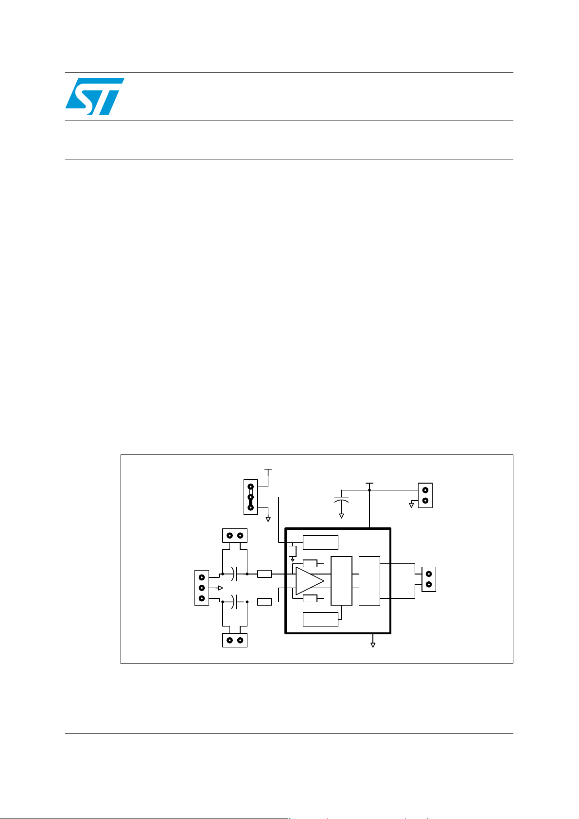
Figure 1. shows the schematic diagram of the demoboard.
Figure 1. Schematic diagram of the mono class D demoboard
Vcc
Positive input
Negative Input
Cn1
Input
Cn4
1
2
3
Cn2
C1
100nF
1
2
GND
3
100nF
C2
Cn3
GND
R1
150k
R2
150k
Stdby
1
4
InIn+
3
-
+
300k
150k
150k
C3
1uF
Internal
Bias
Oscillator
GND
PWM
Vcc
Vcc
Output
H
Bridge
GND
7
GND
6
Out+
Out-
U1
5
8
TS4962DFN
Cn6
Gnd
Cn5
Positive Output
Negative Output
Speaker
April 2007 Rev 2 1/5
www.st.com
AN2406
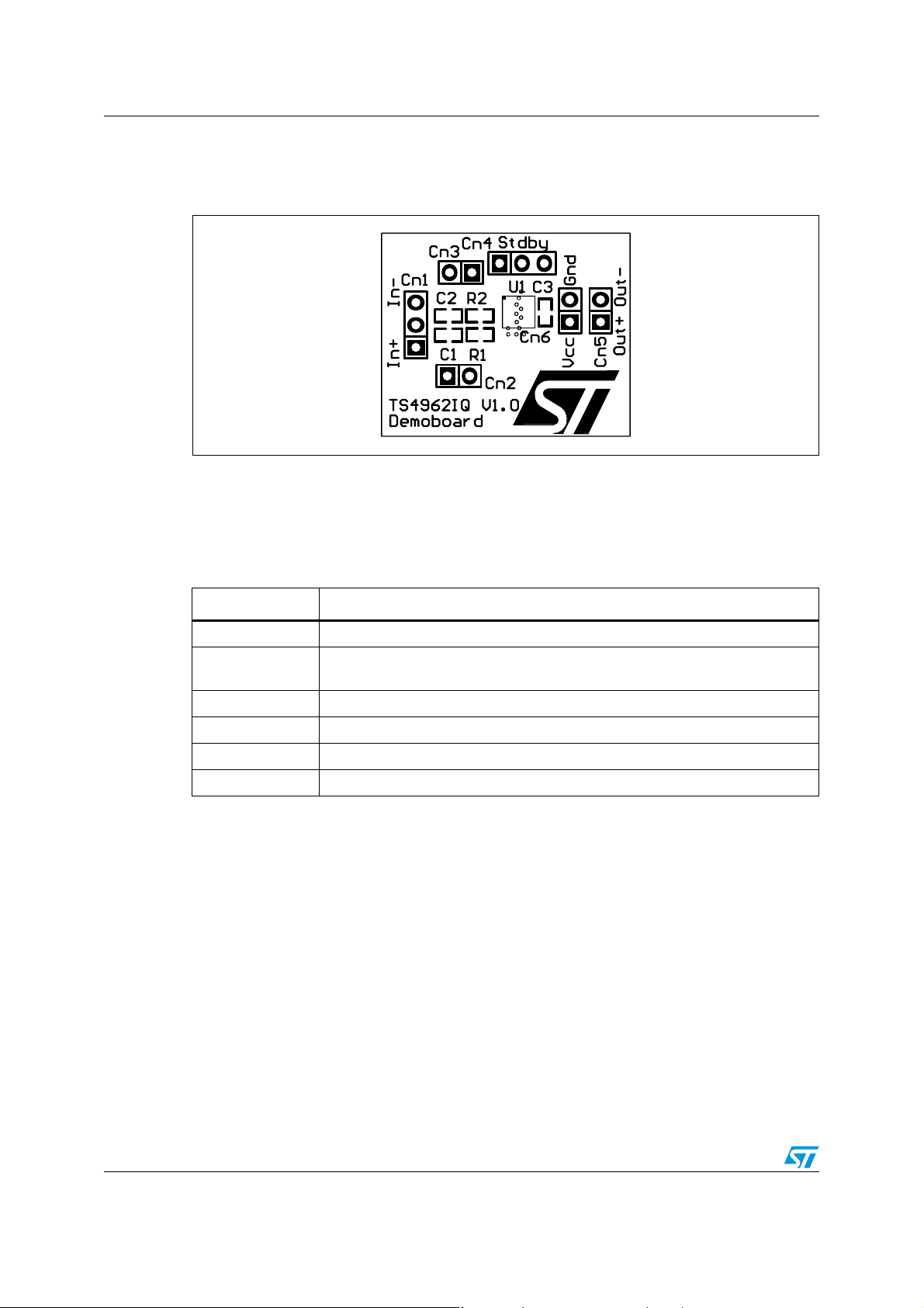
Figure 2. shows the top view of the demoboard PCB, with the markings showing the
connector placements.
Figure 2. Mono class D demoboard - top view
Caution: When you apply the pow er supply throug h Cn6, DO NO T in vert the polarity because it would
destroy the amplifier U1.
Table 1 lists the connectors on the demoboard, with a description for each, and their
configurations.
Table 1. Description of demoboard connectors and their configurations
Connectors Description
Cn1 Input signal connector (active input signal positive and negative)
Cn2 and Cn3
Connectors to modify input configuration (from capacitor-coupled = no jumper to
common mode feedback = short-circuit).
Cn5 Output signal connector (Vo+ and Vo-)
Cn4 Standby control connector (GND, Standby, VCC)
Cn6 Power connector (V
and GND). Power supply voltage from 2.4V to 5.5V.
CC
U1 Class D amplifier TS4962IQ
2/5

AN2406
A list of the components mounted on the demoboard is given in Table 2.
Table 2. Component list for the mono class D demoboard
Designation Quantity Description
C1 1 100nF/10V X7R/0603 capacitor
C2 1 100nF/10V X7R/0603 capacitor
C3 1 1μF/10V, X5R/0603 capacitor
Cn1 1 3 pins header 2.54mm pitch
Cn2 1 2 pins header 2.54mm pitch
Cn3 1 2 pins header 2.54mm pitch
Cn4 1 3 pins header 2.54mm pitch
Cn5 1 2 pins header 2.54mm pitch
Cn6 1 2 pins header 2.54mm pitch
R1 1 150k, 1/16W/0603 1% resistor
R2 1 150k, 1/16W/0603 1% resistor
U1 1 TS4962IQ
Figure 3 and Figure 4 show the demoboard PCB layers.
Figure 3. PCB bottom layer Figure 4. PCB top layer
3/5

Configuring the demoboard characteristics AN2406
Configuring the demoboard characteristics
Differential gain
The demoboard is set up with the differential gain AV set to 2V/V.
If necessary , the diff erential gain can be adapted b y modifying the v alues of resistors R1 and
R2, in accordance with the following relation:
where R1=R2 in kΩ.
Input configuration
On the demoboard, the Cn2 and Cn3 jumpers allow you to change the input configuration
between capacitor-coupled and common-mode feedback.
In the capacitor-coupled configuration, the -3dB cut-off frequency in Hz is:
with R in Ohms, C in Farads and C1=C2.
More information about component calculations is available in the TS4962 datasheet.
Revision history
Date Revision Changes
300kΩ
-----------------
A
v
1
R1
××π
or =
=
CR2
300kΩ
A
-----------------=
v
R2
1
CR2
××π
2211
28-Jul-2006 1 Initial release.
12-Apr-2007 2 Updated
4/5
Table 2: Component list for the mono class D demoboard.

AN2406
Please Read Carefully:
Information in this document is provided solely in connection with ST products. STMicroelectronics NV and its subsidiaries (“ST”) reserve the
right to make changes, corrections, modifications or improvements, to this document, and the products and services described herein at any
time, without notice.
All ST products are sold pursuant to ST’s terms and conditions of sale.
Purchasers are solely res ponsibl e fo r the c hoic e, se lecti on an d use o f the S T prod ucts and s ervi ces d escr ibed he rein , and ST as sumes no
liability whatsoever relati ng to the choice, selection or use of the ST products and services described herein.
No license, express or implied, by estoppel or otherwise, to any intellectual property rights is granted under this document. If any part of this
document refers to any third pa rty p ro duc ts or se rv ices it sh all n ot be deem ed a lice ns e gr ant by ST fo r t he use of su ch thi r d party products
or services, or any intellectua l property c ontained the rein or consi dered as a warr anty coverin g the use in any manner whats oever of suc h
third party products or servi ces or any intellectual property contained therein.
UNLESS OTHERWISE SET FORTH IN ST’S TERMS AND CONDITIONS OF SALE ST DISCLAIMS ANY EXPRESS OR IMPLIED
WARRANTY WITH RESPECT TO THE USE AND/OR SALE OF ST PRODUCTS INCLUDING WITHOUT LIMITATION IMPLIED
WARRANTIES OF MERCHANTABILITY, FITNESS FOR A PARTICUL AR PURPOS E (AND THEIR EQUIVALE NTS UNDER THE LAWS
OF ANY JURISDICTION), OR INFRINGEMENT OF ANY PATENT, COPYRIGHT OR OTHER INTELLECTUAL PROPERTY RIGHT.
UNLESS EXPRESSLY APPROVED IN WRITING BY AN AUTHORIZED ST REPRESENTATIVE, ST PRODUCTS ARE NOT
RECOMMENDED, AUTHORIZED OR WARRANTED FOR USE IN MILITARY, AIR CRAFT, SPACE, LIFE SAVING, OR LIFE SUSTAINING
APPLICATIONS, NOR IN PRODUCTS OR SYSTEMS WHERE FAILURE OR MALFUNCTION MAY RESULT IN PERSONAL INJ URY,
DEATH, OR SEVERE PROPERTY OR ENVIRONMENTAL DAMAGE. ST PRODUCTS WHICH ARE NOT SPECIFIED AS "AUTOMOTIVE
GRADE" MAY ONLY BE USED IN AUTOMOTIVE APPLICATIONS AT USER’S OWN RISK.
Resale of ST products with provisions different from the statements and/or technical features set forth in this document shall immediately void
any warranty granted by ST fo r the ST pro duct or serv ice describe d herein and shall not cr eate or exten d in any manne r whatsoever , any
liability of ST.
ST and the ST logo are trademarks or registered trademarks of ST in various countries.
Information in this document su persedes and replaces all information previously su pplied.
The ST logo is a registered trademark of STMicroelectronics. All other names are the property of their respective owners.
© 2007 STMicroelectronics - All rights reserved
STMicroelectronics group of compan ie s
Australia - Belgium - Brazil - Canada - China - Czech Republic - Finland - France - Germany - Hong Kong - India - Israel - Italy - Japan -
Malaysia - Malta - Morocco - Singapore - Spain - Sweden - Switzerland - United Kingdom - United States of America
www.st.com
5/5
 Loading...