

Page 1

AN2394
Application note
STR7/STR9 audio generation with PWM
Introduction
The purpose of this application note is to provide a hardware and firmware solution to STR7
and STR9 microcontroller users for audio playback of a .WAV file.
The approach is optimized in that it uses a minimal number of components external to the
microcontroller, and offers a high degree of flexibility to the end-user for use with their own
.WAV files. There are two .WAV file parameters that can be controlled by the user; the
sample rate and the file size which depends on the application requirements. The actual
content of the .WAV file is irrelevant and may consist of speech, music, etc., and the only
limitation is the audio format. In fact, this application assumes that the .WAV file format must
be: PCM (no compression), 8000/11025/22050/44100 Hz sample rate, 8-bit and mono.
This document is structured as follows: a brief description of the .WAV file format in
Section 1. Section 2 provides a detailed description of the basics of audio playback. Finally,
Section 3 presents in detail an example of an application built around an STR711F
microcontroller and that can be easily tailored to any other STR7/STR9 microcontroller.
December 2007 Rev 1 1/13
www.st.com
Page 2

Contents AN2394
Contents
1 .WAV file format . . . . . . . . . . . . . . . . . . . . . . . . . . . . . . . . . . . . . . . . . . . . . 3
2 Audio playback . . . . . . . . . . . . . . . . . . . . . . . . . . . . . . . . . . . . . . . . . . . . . 4
2.1 STRx PWM description . . . . . . . . . . . . . . . . . . . . . . . . . . . . . . . . . . . . . . . 4
2.2 Audio playback . . . . . . . . . . . . . . . . . . . . . . . . . . . . . . . . . . . . . . . . . . . . . . 5
3 Implementation example with STR711F . . . . . . . . . . . . . . . . . . . . . . . . . 7
3.1 Hardware description . . . . . . . . . . . . . . . . . . . . . . . . . . . . . . . . . . . . . . . . . 7
3.2 Firmware description . . . . . . . . . . . . . . . . . . . . . . . . . . . . . . . . . . . . . . . . . 9
4 Conclusion . . . . . . . . . . . . . . . . . . . . . . . . . . . . . . . . . . . . . . . . . . . . . . . . 11
5 Revision history . . . . . . . . . . . . . . . . . . . . . . . . . . . . . . . . . . . . . . . . . . . 12
2/13
Page 3

AN2394 .WAV file format
1 .WAV file format
The .WAV file format is a subset of the Resource Interchange File Format (RIFF)
specification used for the storage of multimedia files. A RIFF file starts with a file header
followed by a sequence of data chunks. A .WAV file is often just a RIFF file with a single
"WAVE" chunk consisting of two sub-chunks:
1. a fmt chunk specifying the data format
2. a data chunk containing the actual sample data.
The numerical format used is Little-Endian (least significant byte first) and Big-Endian (most
significant byte first) order.
The WAVE file format starts with the RIFF header:
Endian Offset Length Contents
big 0 4 bytes 'RIFF' // 0x52494646
little 4 4 bytes <file length - 8>
big 8 4 bytes 'WAVE' // 0x57415645
Next, the fmt chunk describes the sample format:
big 12 4 bytes 'fmt ' // 0x666D7420
little 16 4 bytes 0x00000010 // Length of the fmt data (16 bytes)
little 20 2 bytes 0x0001 // Format tag: 1 = PCM
little 22 2 bytes <channels> // Channels: 1 = mono, 2 = stereo
little 24 4 bytes <sample rate> // Samples per second: e.g., 22050
little 28 4 bytes <bytes/second> // sample rate * block align
little 32 2 bytes <block align> // channels * bits/sample / 8
little 34 2 bytes <bits/sample> // 8 or 16
Finally, the data chunk contains the sample data:
big 36 4 bytes 'data' // 0x64617461
little 40 4 bytes <length of the data block>
little 44 * <sample data>
This application assumes that the .WAV file to be played has the following format:
● Audio Format: PCM (an uncompressed wave data format in which each value
represents the amplitude of the signal at the time of sampling.)
● Sample rate: may be 8000, 11025, 22050 or 44100 Hz.
● Bits Per Sample: 8-bit (Audio sample data values are in the range [0-255] ).
● Number Of Channels: 1 (Mono)
3/13
Page 4
Audio playback AN2394
2 Audio playback
The audio playback requires two dedicated timers:
● Timer used as system timer, SysTimer: generates an interrupt at a programmable rate
(fixed by the .WAV file sample rate value).
● Timer used in PWM mode. This timer should be able to produce high frequency PWM
signal.
The .WAV file data can be stored in a compatible SPI-based Flash (requiring an SPI
interface), in internal Flash memory (if the chosen STR7/SRT9 MCU has sufficient capacity)
or on any other external memory type supported by the microcontroller .
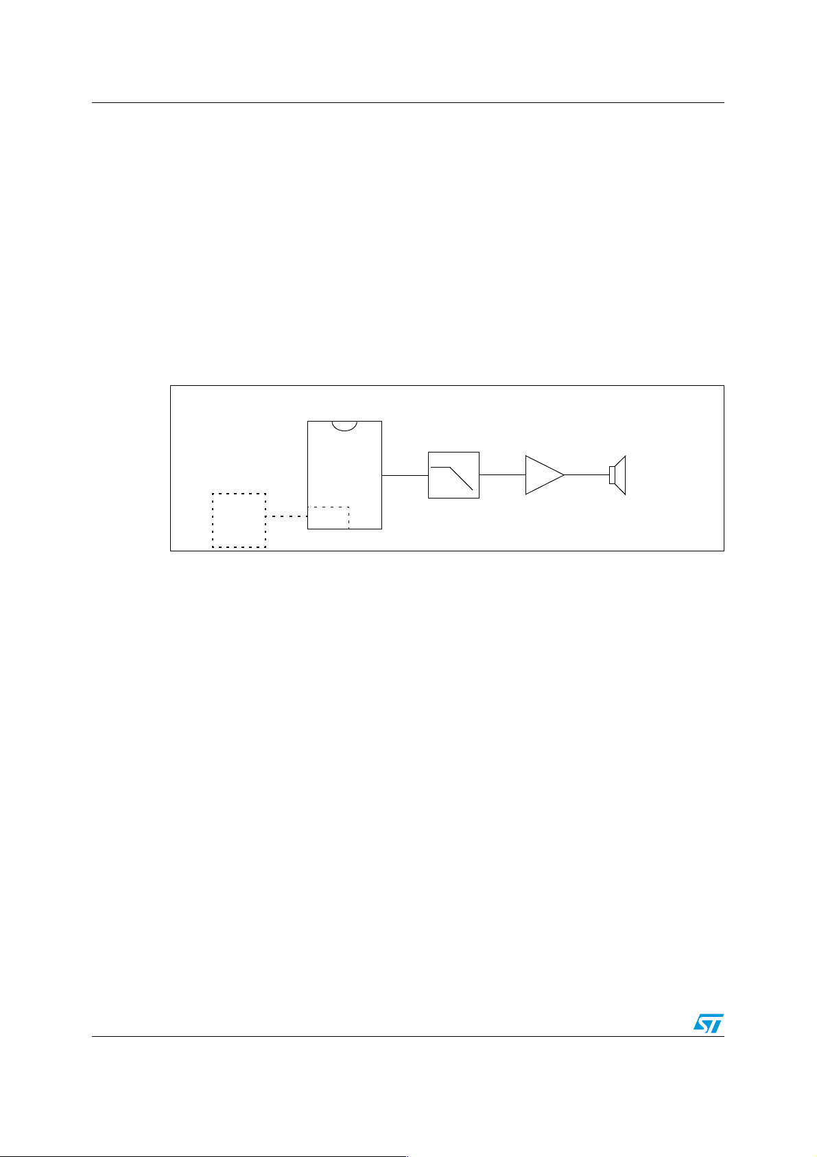
The audio playback flow is presented in the following figure:
Figure 1. Audio playback flow
STR7/STR9
Low-Pass
filter
Audio
Amplifier
Speaker
External Memory,
example: SPI Flash
.WAV
OR
Internal
PWM
.WAV
Flash
To playback the audio, the microcontroller reads each 8-bit sample and then outputs it to a
digital-to-analog converter (DAC) at the desired sample rate. The analog wave produced by
the DAC is amplified and fed to a speaker to produce the sound.
As the STR7/STR9 MCU doesn't have an on-chip DAC, an alternative method is used to
implement 1 channel DAC. Such a method is the use of the built-in Pulse Width Modulation
(PWM) module to generate a signal whose pulse width is proportional to the amplitude of
the sample data. The PWM output signal is then integrated by a low-pass filter to remove
high frequency components, leaving only the low-frequency content. The output of the lowpass filter provides a reasonable reproduction of the original analog signal.
2.1 STR7/STR9 PWM description
This section introduces the basic concepts of the PWM mode of the STR7/STR9 TIMER
(TIM).
Pulse Width Modulation (PWM) consists of a signal with a fixed period whose duty cycle is
variable. The duty cycle represent the ratio of ON period to the period of the signal.
For the TIM, the PWM period and duty cycle are determined by the value of the OCAR and
OCBR registers.
The PWM output signal period is fixed by the OCBR which determines the maximum value
that the counter can count before starting a new period:
T = OCBR * Prescaler * T
4/13
Timer
Page 5

AN2394 Audio playback
Where:
OCBR: Output Compare B register value
Prescaler: Timer clock prescaler
T
: period of the Timer clock that drives the Prescaler.
Timer
The value set in the OCAR determines the duty-cycle:
T
= OCAR * Prescaler * T
d
cycle
on
= (Ton/ T)*100 = (OCAR / OCBR) *100 %
Timer
Where:
OCAR: Output Compare A register value
Figure 2. Typical PWM signal waveform
PWM
Output
d
= 50% d
cycle
= 25% d
cycle
cycle
= 75%
2.2 Audio playback
Before the audio data can be played, the header must be parsed so that the sampling rate of
the data and its length can be determined.
The task of reproducing audio is achieved by using sampled data (data contained in the
.WAV file) to vary the duty cycle of the PWM signal who’s period is held at a constant value.
The duty cycle represents the ratio of the pulse width to the pulse period, i.e. it represents
the ratio of the OCAR value to the OCBR one.
As the duty cycle varies according to the values of the sampled data and this data is coded
in 8 bits (with values from 0 to 255), the OCBR value must be set to 255 and the OCAR
value fills with the sampled data values (the OCAR value varies from 0 to 255). In this
manner the duty cycle varies from 0% to 100%.
The OCAR value is updated at intervals specified by the SysTimer period which is equal to
the sample rate of the .WAV file.
The PWM output signal is then fed to a simple RC low-pass filter to generate an output
voltage directly proportional to the average time spent in the HIGH state (i.e., 50% duty
cycle is equal to 1.65V when VDD = 3.3V). When this is averaged over time, we get a
reasonable reproduction of the original analog signal.
Ton
Ton
T
T
Ton
T
t
There are several design considerations involved in the selection of the cut-off frequency of
the low-pass filter. Primarily, the filter cut-off frequency must be much lower than the PWM
frequency to reduce the noise generated by PWM switching. A PWM frequency of 10 times
the cut-off frequency is a generally sufficient. However, the cut-off frequency of the filter is
critical to the bandwidth of the output audio.
In addition, it is recommended, on the basis of the Nyquist Criterion, that the cut-off
frequency of any filter used be set at half the frequency of the sample playback rate. Since in
5/13
Page 6

Audio playback AN2394
this application different sample rates are supported (8000/11025/22050/44100 Hz), we
must take into account the bandwidth limitation imposed by the lower sample rate.
From a hardware standpoint, a higher PWM frequency is easier to filter, but it corresponds to
a smaller reload value and therefore results in lower resolution. By contrast, a smaller PWM
frequency is difficult to filter; besides, the lower limit is dictated by the data input rate.
Incorporating this guideline, the filter cut-off frequency is set to 4 kHz. This ensures that
almost the entire audio spectrum is passed through, but the PWM carrier is removed.
The values for R and C are computed with this following formula:
1
f
--------------- -=
2π RC
where f is the cut-off frequency of the filter.
6/13
Page 7

AN2394 Implementation example with STR711F
3 Implementation example with STR711F
This section describes a hardware and firmware solution of .WAV file playback implemented
for the STR711F microcontroller and that can be easily tailored to any other STR7/STR9
microcontroller.
The following STR711F peripherals are used:
● TIM0 in Output Compare timing mode to act as SysTimer. The TIM0 global interrupt
can be linked to IRQ (Interrupt Request) channel0 or to FIQ (Fast Interrupt Request)
channel0. For fast, low latency interrupt handling, FIQ channel0 is used to handle TIM0
interrupts.
● TIM3 in PWM mode.
● BSPI0 to communicate with the SPI Flash.
3.1 Hardware description
The electrical schematic of the circuit, which the proposed application refers to is shown in
Figure 3.
An M25P64 SPI-based Flash memory is used to store and send back the .WAV file data to
the ICU. The M25P64 is a 64-Mbit (8M x 8) Serial Flash memory from STMicroelectronics,
accessed by a high speed SPI-compatible bus.
The connection scheme between the microcontroller and the SPI Flash is as the following:
pin S0.SCLK(P0.2) is connected to the Serial Clock pin (C) for data synchronization, pin
S0.MOSI(P0.1) and pin S0.MISO(P0.0) are connected, respectively, to Serial Data Input pin
(D) and Serial Data Output pin (Q) for data transmission. To select and deselect the Flash,
its Chip Select pin (S
The T3.OCMPA pin (P1.2) is used to output the PWM signal. This signal is passed through
a simple low-pass RC (R33 and C15) filter. The cut-off frequency of this filter is set at 4 kHz.
This ensures that almost the entire audio spectrum is passed through, but the PWM carrier
is cut off.
Since the cut-off frequency of the low-pass filter is set at 4kHz, the R and C component
values are calculated as: R = 1.2 kΩ, C = 33 nF.
The filter output is fed to the input of a common TS4871 audio amplifier through a
potentiometer to allow continuous control of the audio volume.
The TS4871 is a monolithic integrated audio power amplifier chip from STMicroelectronics
capable of delivering 0.5W of output power into an 8ohm load at 3V3. The amplifier output is
used to drive an 8ohm speaker.
) is dynamically driven by P1.1 pin.
7/13
Page 8

Implementation example with STR711F AN2394
Figure 3. Audio playback with STR711F
CK
10K
6
10nF
C6
SW-PB (Reset)
S1
4 3
100K
R1
+3V3
5
+3V3
4
3
2
38
1.0uF
C3
29
26
30
25
18
39
8
44
50
59
4
57
28
58
27
33nF
C2
C1
10uF
+3V3
5
1 2
CK
CK
nRSTIN
20
24
21
47
23
22
3
19
17
51
9
CK
V33
V33
V33
V33
AVDD
AVSS
VSS
VSS
VSS
VSS
VSS
VSS
VSS
VSS18
VSS18
V18
V18
52
SPI_MISO
10K
R4
P0.12
HCLK
nRSTIN
RTCXTI
nSTDBY
RTCXTO
V18BKP
VSSB KP
STR711F
P0.3/S0.SSN55P0.0/S0.MISO
P0.1/S0.MOSI53P0.2/S0.SCLK
P1.536P1.334P1.435P1.6
P1.740P1.8
P1.2/T3. OCMPA /AIN2
54
37
41
33
SPI_MOSI
SPI_SCLK
PWM
Audio_Out
R4
X2
3
CK
+3V3
61
63
5
1
48
P0.6
P0.8
P0.13
P0.10
P1.14
P0.15/W AKEUP
P0.9
P0.5
P0.7
P0.11
P1.9
2
64
60
62
45
2
3
4
+3V3
TEST
NU
nJTR ST
JTDO
JTCK
JTMS
JTDI
BOOTEN
USBDP
USBDN
P1.0
P1.1
P1.15
P1.10
P0.14
P0.4
2
1
4
4 MHz OSC
1
+3V3
1 2
3 4
5 6
7 8
9 10
11 12
13 14
15 16
17 18
19 20
J1
10K
R8
10K
R7
10K
R6
10K
R5
nJRTST
JTDI
JTMS
16
15
nJRTST
14
JTDO
13
JTCK
12
JTMS
11
10
JTDI
10K
7
42
43
31
32
49
46
6
56
C9
R27
BOOTEN
SPI_CS
KDMG15008- 03
SP1
+3V3
2
1
6
5
8
Uout1
Vout2
470pF
100K
R35
Standby1Bypass2Vin+3Vin-
U1
4
HEADER 10 X2
10K
R30
10K
R29
JTCK
JTDO
2.2K
R28
nRSTIN
100uF
C19
100nF
C18
7
VCC
GND
TS4871 IST
2.2uF
C17
6
5
4
3
2
SPI_SCLK
SPI_MOSI
+3V3
4
6
3
D5C
W
VSS
HOLD7VCC8S1Q
U2
2
100nF
C14
+3V3
1
A A
M25P6 4-VM E6G
SPI_MISO
SPI_CS
B B
8/13
22K
R34
C16
2
50K
RV1
13
C15
1.2K
R33
Audio_ Out
C C
150nF
33nF
1
D D
Page 9

AN2394 Implementation example with STR711F
3.2 Firmware description
The software associated with this application is developed in C using the STR71x Firmware
Library from STMicroelectronics. The STR71x Firmware Library provides a set of functions
covering the functionality of the STR71x peripheral. As a result, users can develop
applications for any STR71x device without an in-depth study of each peripheral
specification.
Note: The firmware assumes that the .WAV file is stored at address 0x00 of the Flash.
The first part of the software performs the configuration of the different system clocks. The
main clock (MCLK), PCLK1 (including serial communication peripherals, such as BSPI0)
and PCLK2 (including system peripherals, such as TIM0 and TIM3) are set to 32MHz using
an external 4MHz oscillator.
Once the BSPI0 peripheral and its associated pin are configured, the baudrate is set to
5.3Mb/s.
The task of audio playback is achieved by calling the WAVE_PlayBack function. This
function starts by a call to the WAVE_Parsing function. This checks the format of the .WAV
file and gets information about the audio format. This is done by reading the value of a
number of parameters stored in the file header and comparing these to the values expected
for the format of a standard .WAV file. If a valid .WAV file format, it continues reading the
header to determine the audio format in terms of the sample rate and the sampled data size.
If the audio format is supported by this application, it retrieves the audio format in the
WAVE_FormatTypeDef structure and returns a zero value. Otherwise the function fails and
the return value is nonzero. In this case, the return value specifies the cause of the function
fails.
The WAVE_PlayBack function tests the value returned by WAVE_Parsing function, if it is a
nonzero value the audio playback fails. Otherwise, it configures the TIM0 and TIM3 timers.
TIM3 is programmed to generate 125.5kHz PWM signal and TIM0 is programmed to
generate an interrupt at frequency equal to the .WAV file sample rate value.
Note: As TIM3 OCBR value is fixed to 255, the maximum PWM frequency that can be reached is
125.5kHz.
On each TIM0 interrupt, a byte is read from the SPI Flash to update the TIM3 Output
Compare A register (OCAR) value. A counter loop operates by counting down from the
sampled data size value and when zero is reached the playback is stopped.
Usually, to read a byte from the SPI Flash several steps are performed:
1. Drive the S
2. Send read data instruction
3. Send a 3 byte address
4. Send a dummy byte. Then the memory content, at that address, is shifted out on Serial
Data Output (Q)
5. Drive the S
Repeating this procedure for each byte read from the SPI Flash increases the processing
time of the TIM0 interrupt service routine. This can affect the CPU load and limits other
tasks that the application may demand.
line low to select the device
line high to deselect the device
9/13
Page 10

Implementation example with STR711F AN2394
To avoid this and decrease the CPU load, a solution based on the capability to read the
whole SPI Flash memory with a single read data instruction is implemented:
– the first time a data byte is needed, a call to Start_Read_Sequence function is
made. This initiates a read data byte sequence from the SPI Flash. This is done by
driving the S
transmitted followed by 24-bit address. This function exits and keeps the S
line low to select the device, then the read data instruction is
line
low, with the SPI Flash still being selected.
The next routine which needs to read a byte from the SPI Flash has only to generate a
dummy byte on the Serial Data Input line of the SPI Flash and get the data on the Serial
Data Output line. So only step 4 is performed each time a data is read from the SPI Flash
which significantly reduces the CPU overhead.
When the playback is finished, the read data byte sequence is terminated by driving Chip
Select high.
10/13
Page 11

AN2394 Conclusion
4 Conclusion
This document proposes a straightforward and flexible solution to use a member of the STR
family, STR711F, for playback of a .WAV file stored in an SPI Flash memory. This can be
used in many applications where high-performance audio playback is not required such as:
talk back units, man-machine interfacing and low-cost music players.
11/13
Page 12

Revision history AN2394
5 Revision history
Table 1. Document revision history
Date Revision Changes
06-Dec-2007 1 Initial release.
12/13
Page 13

AN2394
Please Read Carefully:
Information in this document is provided solely in connection with ST products. STMicroelectronics NV and its subsidiaries (“ST”) reserve the
right to make changes, corrections, modifications or improvements, to this document, and the products and services described herein at any
time, without notice.
All ST products are sold pursuant to ST’s terms and conditions of sale.
Purchasers are solely responsible for the choice, selection and use of the ST products and services described herein, and ST assumes no
liability whatsoever relating to the choice, selection or use of the ST products and services described herein.
No license, express or implied, by estoppel or otherwise, to any intellectual property rights is granted under this document. If any part of this
document refers to any third party products or services it shall not be deemed a license grant by ST for the use of such third party products
or services, or any intellectual property contained therein or considered as a warranty covering the use in any manner whatsoever of such
third party products or services or any intellectual property contained therein.
UNLESS OTHERWISE SET FORTH IN ST’S TERMS AND CONDITIONS OF SALE ST DISCLAIMS ANY EXPRESS OR IMPLIED
WARRANTY WITH RESPECT TO THE USE AND/OR SALE OF ST PRODUCTS INCLUDING WITHOUT LIMITATION IMPLIED
WARRANTIES OF MERCHANTABILITY, FITNESS FOR A PARTICULAR PURPOSE (AND THEIR EQUIVALENTS UNDER THE LAWS
OF ANY JURISDICTION), OR INFRINGEMENT OF ANY PATENT, COPYRIGHT OR OTHER INTELLECTUAL PROPERTY RIGHT.
UNLESS EXPRESSLY APPROVED IN WRITING BY AN AUTHORIZED ST REPRESENTATIVE, ST PRODUCTS ARE NOT
RECOMMENDED, AUTHORIZED OR WARRANTED FOR USE IN MILITARY, AIR CRAFT, SPACE, LIFE SAVING, OR LIFE SUSTAINING
APPLICATIONS, NOR IN PRODUCTS OR SYSTEMS WHERE FAILURE OR MALFUNCTION MAY RESULT IN PERSONAL INJURY,
DEATH, OR SEVERE PROPERTY OR ENVIRONMENTAL DAMAGE. ST PRODUCTS WHICH ARE NOT SPECIFIED AS "AUTOMOTIVE
GRADE" MAY ONLY BE USED IN AUTOMOTIVE APPLICATIONS AT USER’S OWN RISK.
Resale of ST products with provisions different from the statements and/or technical features set forth in this document shall immediately void
any warranty granted by ST for the ST product or service described herein and shall not create or extend in any manner whatsoever, any
liability of ST.
ST and the ST logo are trademarks or registered trademarks of ST in various countries.
Information in this document supersedes and replaces all information previously supplied.
The ST logo is a registered trademark of STMicroelectronics. All other names are the property of their respective owners.
© 2007 STMicroelectronics - All rights reserved
STMicroelectronics group of companies
Australia - Belgium - Brazil - Canada - China - Czech Republic - Finland - France - Germany - Hong Kong - India - Israel - Italy - Japan -
Malaysia - Malta - Morocco - Singapore - Spain - Sweden - Switzerland - United Kingdom - United States of America
www.st.com
13/13
 Loading...