

Page 1

AN2386
Application note
How to achieve the threshold voltage thermal coefficient
of the MOSFET acting on design parameters
Introduction
Today, the MOSFET devices are used mainly as switches in electronic circuits. In such
operational conditions, the MOSFET device works in switch on and switch off modes.
However, in some applications, as in audio amplifiers or air conditioning, the MOSFET
works in a linear zone. The MOSFET works in a linear zone when either it is subject to a
high voltage, or a high current passes through the device. As it is well known in literature,
during the linear zone operation mode the MOSFET could fail if a thermal run-away occurs.
The failure conditions depend on either of the internal structure of MOSFET or of the
package used. The threshold voltage thermal coefficient (TVTC) is one of the big elements
that could bring the MOSFET to fail. TVTC is achieved deriving the MOSFET threshold
voltage against the temperature. TVTC is a negative coefficient because of when the
temperature increases the threshold voltage decreases. When TVTC increases in absolute
value, the MOSFET becomes thermally instable and a failure could occur. Therefore, in
order to understand if a MOSFET device can be used in an application working in linear
zone in safety conditions, a device with a low TVTC value must be considered and, thus, it is
important to achieve a theoretical expression for it.
June 2006 Rev 1 1/30
www.st.com
Page 2

Contents AN2386
Contents
1 MOS structure . . . . . . . . . . . . . . . . . . . . . . . . . . . . . . . . . . . . . . . . . . . . . . 5
2 Some considerations on VTH and TVTC equations and real examples .
14
3 Case of DEVICE3 . . . . . . . . . . . . . . . . . . . . . . . . . . . . . . . . . . . . . . . . . . . 25
4 Conclusions . . . . . . . . . . . . . . . . . . . . . . . . . . . . . . . . . . . . . . . . . . . . . . . 27
5 References . . . . . . . . . . . . . . . . . . . . . . . . . . . . . . . . . . . . . . . . . . . . . . . . 28
6 Revision history . . . . . . . . . . . . . . . . . . . . . . . . . . . . . . . . . . . . . . . . . . . 29
2/30
Page 3

AN2386 List of figures
List of figures
Figure 1. Cross section view of a MOS capacitor . . . . . . . . . . . . . . . . . . . . . . . . . . . . . . . . . . . . . . . . 5
Figure 2. Energy band diagram of an ideal MOS capacitor under thermal equilibrium.. . . . . . . . . . . . 5
Figure 3.
Figure 4.
Figure 5.
Figure 6. DEVICE1 V
Figure 7. DEVICE1 TVTC - comparison between simulated and measured data . . . . . . . . . . . . . . . 16
Figure 8. Weight of single term of (Equation 42) on TVTC at different temperatures . . . . . . . . . . . . 17
Figure 9. DEVICE2 V
Figure 10. DEVICE2 TVTC - comparison between simulated and measured data . . . . . . . . . . . . . . . 19
Figure 11. DEVICE1 V
Figure 12. DEVICE1 TVTC simulated data - comparison between different N
Figure 13. DEVICE1 V
Figure 14. DEVICE1 TVTC simulated data - comparison between different N
Figure 15. DEVICE1 V
Figure 16. DEVICE1 TVTC simulated data - comparison between different tox . . . . . . . . . . . . . . . . . 21
Figure 17. DEVICE1 V
Figure 18. DEVICE1 TVTC simulated data - fixing T and acting on N
Figure 19. DEVICE1 V
Figure 20. DEVICE1 TVTC simulated data - fixing T and acting on N
Figure 21. DEVICE1 V
Figure 22. DEVICE1 TVTC simulated data - fixing T and acting on t
Figure 23. V
Figure 24. TVTC simulated data - comparison between DEVICE1 and the new device . . . . . . . . . . . 23
Figure 25. V
Figure 26. TVTC simulated data considering a p-gate doped MOS . . . . . . . . . . . . . . . . . . . . . . . . . . 24
Figure 27. Energy band diagram at low and high doping concentration . . . . . . . . . . . . . . . . . . . . . . . 25
Figure 28. DEVICE3 V
Figure 29. DEVICE3 TVTC - comparison between simulated and measured data . . . . . . . . . . . . . . . 26
Energy band diagram and charge distribution in an ideal MOS capacitor in accumulation condition.. 6
Energy band diagram and charge distribution in an ideal MOS capacitor in accumulation condition. . 6
Energy band diagram and charge distribution in an ideal MOS capacitor in inversion condition . . . . 7
- comparison between simulated and measured data . . . . . . . . . . . . . . . . 16
TH
- comparison between simulated and measured data . . . . . . . . . . . . . . . . 18
TH
simulated data - comparison between different Ng. . . . . . . . . . . . . . . . . . . 19
TH
simulated data - comparison between different Na. . . . . . . . . . . . . . . . . . . 20
TH
simulated data - comparison between different tox. . . . . . . . . . . . . . . . . . . 20
TH
simulated data - fixing T and acting on Ng . . . . . . . . . . . . . . . . . . . . . . . . . 21
TH
simulated data - fixing T and acting on Na . . . . . . . . . . . . . . . . . . . . . . . . . 22
TH
simulated data - fixing T and acting on tox . . . . . . . . . . . . . . . . . . . . . . . . . 22
TH
simulated data - comparison between DEVICE1 and the new device . . . . . . . . . . . . 23
TH
simulated data considering a p-gate doped MOS . . . . . . . . . . . . . . . . . . . . . . . . . . . . 24
TH
- comparison between simulated and measured data . . . . . . . . . . . . . . . . 26
TH
. . . . . . . . . . . . . . . . . . . . . . . . 21
g
. . . . . . . . . . . . . . . . . . . . . . . . 22
a
. . . . . . . . . . . . . . . . . . . . . . . . 23
ox
. . . . . . . . . . . . . . . . . 19
g
. . . . . . . . . . . . . . . . . 20
a
3/30
Page 4

List of tables AN2386
List of tables
Table 1. Main electrical parameter simulated by DEVICE1 . . . . . . . . . . . . . . . . . . . . . . . . . . . . . . . 15
Table 2. Main electrical parameter simulated by DEVICE2 . . . . . . . . . . . . . . . . . . . . . . . . . . . . . . . 17
Table 3. Revision history . . . . . . . . . . . . . . . . . . . . . . . . . . . . . . . . . . . . . . . . . . . . . . . . . . . . . . . . . 29
4/30
Page 5
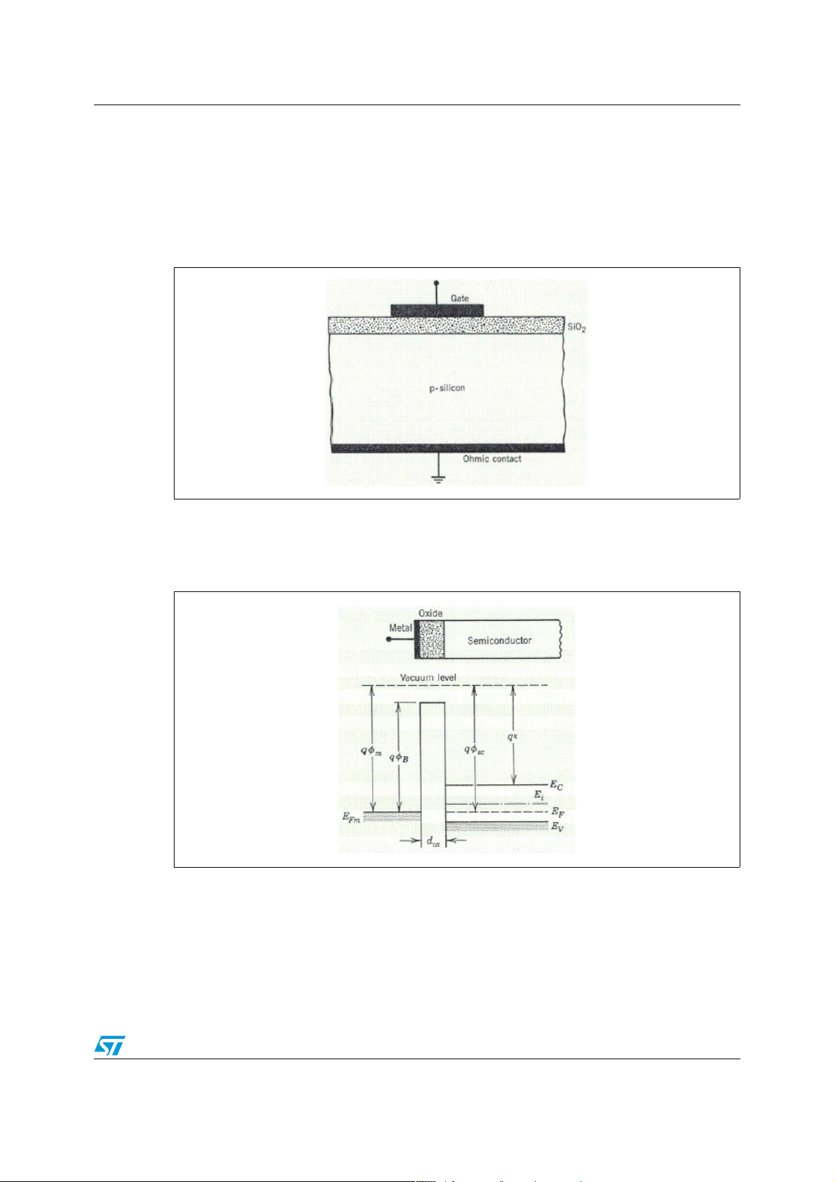
AN2386 MOS structure
1 MOS structure
As it is well known, a MOS structure is composed by three layers: the first one is metal or
heavily doped polycrystalline silicon, the second one is an insulator of SiO
one is the semiconductor (see Figure 1.).
Figure 1. Cross section view of a MOS capacitor
and the third
2
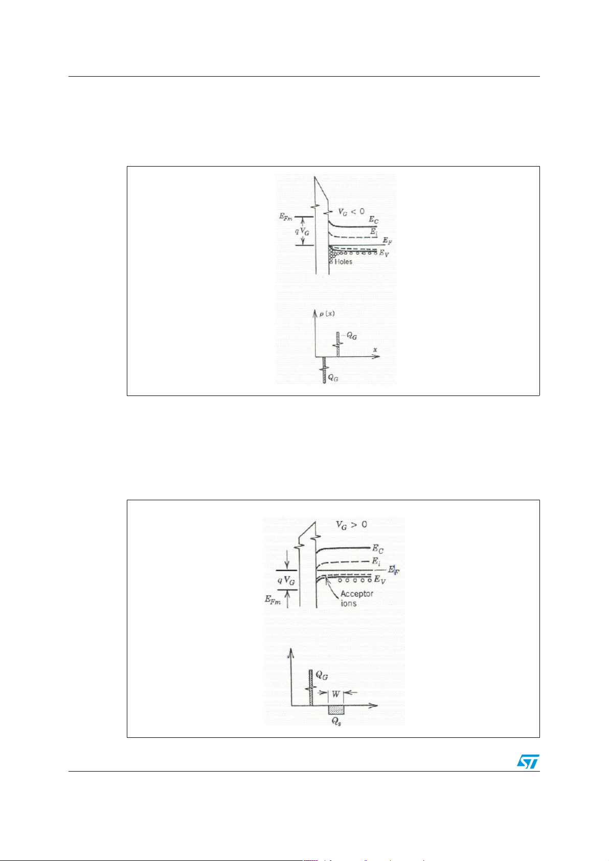
Considering an ideal MOS system with a p-doped semiconductor, the energy band diagram
can be illustrated as in Figure 2.
Figure 2. Energy band diagram of an ideal MOS capacitor under thermal
equilibrium.
q Φ
is the work function (energy that needs to extract an electron from the metal); q ΦB is
m
the energy difference between the oxide conduction band and the metal Fermi energy level
(metal-to-oxide barrier energy); q Φ
is the work function of the semiconductor; q χ is the
sc
energy difference between the vacuum level and the conduction band edge.
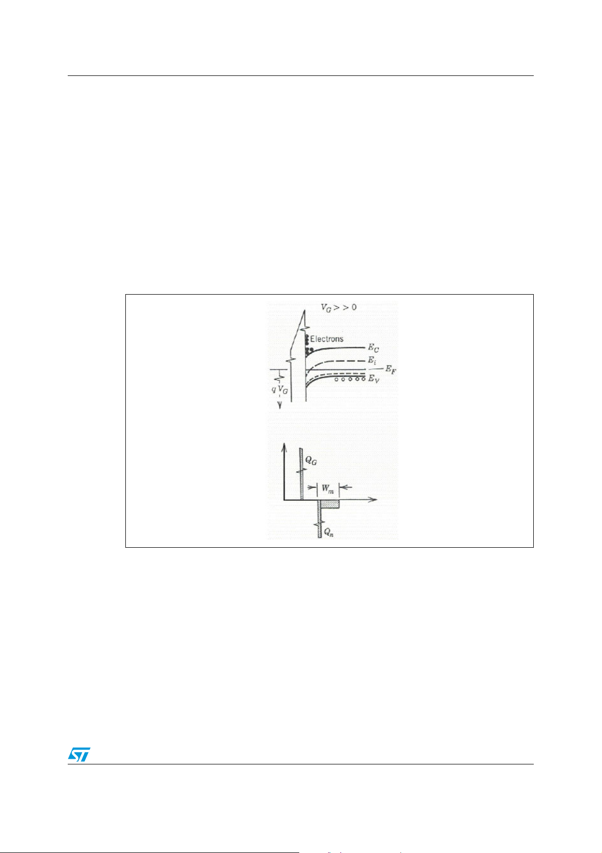
When a negative voltage (V
the Fermi level of the metal raises of qV
) is applied on the gate terminal respect to the semiconductor,
g
compared to the semiconductor side. In moving
g
from the semiconductor to the metal, the vacuum level must bend up gradually to
5/30
Page 6
MOS structure AN2386
accommodate the gate voltage applied. Part of this bending occurs in the semiconductor
and the rest in the oxide. The metal and the semiconductor affinity remain the same (see
Figure 3.).
Figure 3. Energy band diagram and charge distribution in an ideal MOS capacitor
in accumulation condition.
The negative charge on the gate creates an opposite charge on the semiconductor
(enhanced concentration of holes near the oxide interface). When a small positive bias is
applied to the gate, holes are pushed away from the oxide interface and create a depletion
layer in the semiconductor, consisting on the negative charges due to the acceptor ions. The
energy band diagram and the charge distribution are shown in Figure 4.
Figure 4. Energy band diagram and charge distribution in an ideal MOS capacitor
in accumulation condition.
6/30
Page 7
AN2386 MOS structure
The charge Qs in the semiconductor side near the oxide interface is equal to Qg and it can
be written as:
Equation 1
QsqNaW–=
N
is the acceptor concentration and W is the width of the surface depletion layer. Increasing
a
the gate voltage the bands continue to bend downward until E
energy between the conduction and the valence bands) equals E
(the intermediate level
i
(the Fermi energy level)
F
at the surface. In this condition, at the interface near the oxide, the semiconductor becomes
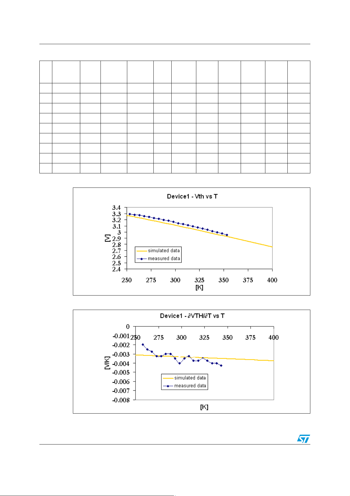
intrinsic. Increasing the gate voltage again, E
crosses EF and, thus, the minority carriers, in
i
this case the electrons, are attracted to the oxide-semiconductor interface. In this new
condition, the surface layer contains more electrons than holes and it becomes n-type
(inversion layer) (see Figure 5.).
Figure 5. Energy band diagram and charge distribution in an ideal MOS capacitor
in inversion condition
Now, Q
can be written as:
s
Equation 2
Q
is the inversion layer charge.
n
Q
Q–
s
qNaW–=
n
The relationships between the band bending, the electron and hole concentrations in the
interface oxide-semiconductor may be obtained assuming that the semiconductor is non
degenerate and that the doping is uniform. The electron and hole concentrations on the bulk
semiconductor can be written respectively as:
Equation 3
φ
F
------ -
–
•
q
kT
7/30
n
0ni
EFEi–
----------------- -
kT
e
==
nie
Page 8

MOS structure AN2386
Equation 4
EFEi–
----------------- -
p0nie
is the intrinsic electron concentration; Ei is the intrinsic Fermi level; EF is the Fermi level; k
n
i
kT
==
is the Boltzmann constant and it is equal to 1.38x10
Considering that the semiconductor is doped of N
φ
F
------ -
•
q
kT
nie
-23
J/K; ΦF is the Fermi potential.
acceptor, (Equation 4) becomes:
a
Equation 5
•
q
nie
------ -
kT
φ
F
Now, it is possible achieve
Φ
F
as:
N
ani
EFEi–
------------------
–
kT
e
==
Equation 6
N
kT
------ -
Φ
F
q
------ -
ln=
a
n
i
For an intrinsic semiconductor ni can be written in two different ways as:
Equation 7
EcEF–
-------------------
–
n
=
iNc
kT
e
Equation 8
EcEF–
-------------------
–
niNVe
=
kT
Multiplying (Equation 7) and (Equation 8) it is possible obtain:
Equation 9
EcEv–
------------------
2
n
NcNVe
i
N
and NV are the effective density of states at the conduction and valence edges
C
respectively and E
is the energy band-gap. NC and NV can be achieved by the electron and
g
kT
NcNve
==
EgT()
---------------
kT
hole distribution functions and they are equal to:
Equation 10
3
-- -
2
2πm
Nc2
--------------------------- -
=
kT•
e
2
h
Equation 11
3
-- -
2
N
m
* and mh* are the electron and hole density of the states effective masses and h is the
e
v
2πm
--------------------------- -
2
=
kT•
h
2
h
Planck constant. The energy band gap depends on the temperature and it can be written as:
Equation 12
E
gEg0b1
T–=
8/30
Page 9

AN2386 MOS structure
where b1 is equal to 4.76 x 10
E
is equal to 1.21eV and it is the extrapolate value of the band-gap at 0°K while b1 is the
g0
-23
J/K.
rate of energy gap shift with temperature. Now, (Equation 9) can be rewritten as:
Equation 13
Eg0b1T–
-------------------------
2
n
NcNVe
i
kT
NcNve
==
b
1
-----
k
E
g0
---------
kT
e
Considering that for the silicon:
Equation 14
b
1
-----
cNV
k
e
3.88 1016• T
N
3
-- -
2
cm3–[]=
and that:
Equation 15
E
g0
---------
14047 K[]=
k
n
becomes:
i
Equation 16
ni3.88 1016• T
3
-- -
–
2
e
E
g0
----------
2kT
3.88 10
• T
16–
3
–
-- -
2
e
7023
-------------
T
cm3–[]==
In the interface layer oxide-semiconductor, the electron and hole concentrations depend on
the gate voltage and can be written as:
Equation 17
n
sn0
EisEi–
------------------
–
kT
e
==
q
•
n0e
------ -
kT
Φ
s
Equation 18
sn0
e
When
n
Φ
is equal to ΦF the semiconductor surface becomes intrinsic. Instead, increasing Φs
s
again, the layer becomes n-type. When n
EisEi–
------------------
–
kT
==
equals to p0 a "strong inversion" occurs and the
s
q
•
n0e
------ -
kT
Φ
s
minority carriers at the surface become the same of the majority carriers in the bulk. The
potential condition for the strong inversion occurs when:
Equation 19
2Φ
=
Φ
s
F
As explained above, when V
is applied on the MOS structure, VOX (a part of VG) will
G
appear across the oxide and the rest on the silicon surface:
Equation 20
V
GVOXΦs
–=
9/30
Page 10

MOS structure AN2386
If no charges are placed inside the oxide and if the MOS structure can be considered as a
simple parallel plate capacitor, its capacitance can be written as:
Equation 21
Q
ε
is the oxide permittivity (34.5x10
ox
Thus, considering (Equation 21), V
A
C
OXεOX
-12
F/m); tOX is the oxide thickness; A is the plate area.
can be written as:
OX
-------- -
•
t
OX
s
---------- -–==
V
OX
Equation 22
Q
V
OX
s
-----------–=
C
OX
and the gate voltage as:
Equation 23
Q
s
-----------– Φ
V
G
+=
OX
s
C
Considering (Equation 2), neglecting Q
, VG can be rewritten as:
n
Equation 24
qNaW
V
---------------- Φ
G
+=
C
OX
s
By applying the Poisson equation in the semiconductor surface, the following equation can
be obtained:
Equation 25
qN
a
----------
∇2Φ==
ε
s
rotE is the electric field rotor; ∇
silicon permittivity (105.4x10
-12
rotE
2
Φ is the voltage space second order derived; and es is the
F/m). From (Equation 25) the following equation can be
achieved:
Equation 26
2
qNaW
-------------------=
Φ
2
2ε
s
and, thus, the depletion layer width can be achieved as:
Equation 27
2ε
---------------=
qN
sΦs
a
W
will became:
V
G
10/30
Page 11

AN2386 MOS structure
Equation 28
G
2εsqNaΦ
-------------------------- - Φ
V
s
+=
C
OX
s
The gate voltage at the strong inversion condition is the threshold voltage V
of the MOS
TH
and it can be written as:
Equation 29
V
TH
4εsqNaΦ
--------------------------- 2Φ
F
+=
C
OX
F
Up to now, the ideal MOS structure was considered. In the real MOS structure, when no
voltage is applied on the gate, a difference between metal and semiconductor work function
exists, as well as charges in the oxide. In this paper, the charges inside the oxide will be
neglected and also the metal-semiconductor difference work function Φ
will be studied.
ms
The charges inside the oxide are related to the real process flow and they involve a small
threshold voltage shift. In order to consider the effect of Φ
on the threshold voltage, the
ms
following formula must be taken into account:
Equation 30
V
THVFBtOX
V
is the flat-band voltage and it is the gate voltage required to bring the semiconductor
FB
bands flat; Q
are the charges inside the oxide. Such voltage equals to Φms when the
OX
4εsqNaΦ
--------------------------- 2ΦFΦ
F
ε
OX
ms
Q
OX
----------- - t
++ +=++=
C
OX
4εsqNaΦ
-------------------------------
• 2Φ
OX
ε
OX
F
F
charges inside the oxide are neglected.
For metal gate, Φ
can be written as:
ms
Equation 31
E
T()
g
--------------- Φ
–=
2q
±+
F
where E
Φ
Φmχ
ms
(T) is the band-gap energy versus the temperature.
g
Instead, for polysilicon gate (the real case usually) of n-type and the semiconductor is of ptype, Φ
can be written as:
ms
Equation 32
N
•
N
is the doping level of the polysilicon.
g
kT
ms
------ -
Φ
gNa
--------------------
ln–=
q
2
ni
TVTC can be, thus, achieved deriving (Equation 30) against the temperature:
Equation 33
∂V
TH
-------------
∂T
∂Φ
ms
------------- t
∂T
OX
4εsqN
------------------------
•
ε
OX
∂Φ
a
------------- -
• 2
∂T
∂Φ
F
F
---------
•++=
∂T
and also:
11/30
Page 12

MOS structure AN2386
Equation 34
∂V
TH
-------------
∂T
∂Φ
ms
------------- t
∂T
OX
εsqN
---------------------
•
εOXΦ
∂Φ
a
---------
• 2
∂T
F
∂Φ
F
F
---------
•++=
∂T
At the beginning, the thermal coefficient of Φ
will be studied.
ms
Deriving (Equation 32), it is possible achieve:
Equation 35
N
•
∂Φ
ms
-------------
∂T
k
gNa
-- -
--------------------
q
2
ni
2kT
----------
qni
∂ni
------- -
•+ln–=
∂T
and, thus:
Equation 36
∂T
ms
Φ
ms
--------- -
T
2kT
----------
qni
∂ni
------- -
•+=
∂T
∂Φ
-------------
Considering (Equation 16) and deriving it versus T is possible obtain:
Equation 37
∂n
-------
∂T
E
g0
1
-----------
-- -
3
i
-- -
3.88 10
2
•• T
2KT
16
2
e
3.88 1016• T
E
3
-----------
-- -
2KT
2
e
g0
•+=
and also:
Equation 38
n
∂n
-------
∂T
i
i
------ -
2T
E
g0
---------+•=
3
KT
E
g0
--------------
2KT
2
Replacing (Equation 38) in (Equation 36) it is possible obtain:
Equation 39
∂Φ
ms
-------------
∂T
Φ
ms
--------- - 3
T
E
K
g0
--- -
---------++=
q
qT
Now, the thermal coefficient of the Fermi voltage is studied. In fact, deriving (Equation 6) it is
possible achieve:
Equation 40
∂Φ
---------
∂T
N
K
--- -
q
a
------ -
n
i
F
KT
------- -
qn
∂n
i
-------
•–ln=
∂T
i
Replacing (Equation 38) in (Equation 40), the following equation can be achieved:
Equation 41
∂Φ
---------
∂T
Φ
------
3
F
-- -
2
T
F
E
K
go
--- -
•–
---------- -–=
q
2qT
Replacing (Equation 41) and (Equation 39) in (Equation 34), TVTC can be rewritten as:
Equation 42
∂V
TH
-------------
∂T
Φ
ms
--------- - 2
T
Φ
F
------
• t
T
OX
εsqN
---------------------
•
εOXΦ
∂Φ
a
F
---------
•++=
∂T
F
12/30
Page 13

AN2386 MOS structure
If the silicon is doped of p-type (n-channel MOSFET) and the polysilicon is also doped of ptype, (Equation 32), Φ
becomes positive and it can be rewritten as:
ms
Equation 43
Φ
and (Equation 39) becomes negative:
Equation 44
∂Φ
-------------
∂T
and, thus, (Equation 42) becames:
Equation 45
∂V
-------------
∂T
TH
Φ
ms
--------- - 2
T
Φ
------
• t
T
ms
F
ms
N
kT
------ -
--------------------
ln=
q
Φ
ms
--------- - 3
T
εsqN
---------------------
•
OX
εOXΦ
•
gNa
2
ni
K
--- -
•–
q
a
F
E
go
---------–=
qT
∂Φ
F
---------
• 6
∂T
K
--- -
•– 2
q
E
go
---------
•–++=
qT
13/30
Page 14

Some considerations on VTH and TVTC equations and real examples AN2386
2 Some considerations on VTH and TVTC equations
and real examples
Looking at (Equation 30) it is possible see that the threshold voltage is the sum of three
components: the metal-oxide work function (it is negative when the polysilicon is of n-type
and the silicon substrate is of p-type, while, it is positive when the polysilicon is of p-type),
two times the Fermi potential (it is positive for p-type silicon substrate) and the voltage drop
on the oxide (it is positive for a p-type silicon substrate). TVTC (see Equation 42) also
depends on three contributes: the metal-oxide work function divided by the temperature (it is
a negative value for n-type gate doped in p-type silicon), two times the Fermi potential
divided by the temperature (for a p-type silicon it is a positive value) and a third contribute
function of the Fermi potential thermal coefficient and other parameters as the oxide
thickness and the body concentration of impurity (it is a negative contribute because of its
negative the Fermi potential thermal coefficient).
Considering low voltage power MOSFETs working in linear zone in applications like air fans,
it is important have devices with standard threshold voltage (around 3V in ambient
temperature) and very low TVTC in absolute value, in order to avoid the thermal instability
behavior that could bring the component to fail.
The modern MOSFETs have TVTC in the negative value range (it becomes more negative
when the temperature increases). Therefore, when the device works in linear zone, a power
pulse is dissipated on the component, the temperature increases, the threshold voltage
decreases and the drain current rises.
To avoid the thermal run-away of the device, it is important to minimize the TVTC in absolute
value. The parameters that make TVTC negative, considering an n-type gate and p-type
silicon, are the metal-oxide work functions divided by the temperature and the term of the
Fermi potential thermal coefficient. Instead, the parameter that makes TVTC positive is the
Fermi potential divided by the temperature (T). As shown in (Equation 32), the metal-oxide
work function divided by T depends on the doping concentration of the gate, silicon and the
intrinsic carrier concentration. This parameter increases in absolute value, increasing the
doping concentration of the gate or substrate, while it decreases in absolute value when the
temperature increases because of the intrinsic carrier concentration increases too. In order
to minimize this parameter, the gate and substrate doping concentration must be lowered.
The Fermi potential divided by T depends on the doping concentration of the substrate and
the intrinsic concentration of the carriers. When the doping concentration of the substrate
increases, the parameter also increases its value. By increasing the temperature, the
parameter decreases because the intrinsic carrier concentration increases. In order to
maximize the parameter, the substrate doping concentration should be increased.
The threshold voltage thermal coefficient (see Equation 41) depends on the Fermi potential
divided by T, minus a constant and minus a term function of the inverse of T. Its value is
negative because the parameter with the minus sign is generally higher than the term, due
to the Fermi potential divided by T. When the temperature increases, the parameter also
increases in absolute value because the Fermi potential decreases too. Thus, in order to
minimize the Fermi potential thermal coefficient, the substrate doping concentration must be
increased. However, the third term of (Equation 42), as previously explained, also depends
on the substrate doping concentration root-square. Therefore, considering the modern
MOSFET technology, this term increases in absolute value when the substrate doping
concentration also increases.
14/30
Page 15

AN2386 Some considerations on VTH and TVTC equations and real examples
In the modern device, it is possible to observe that TVTC (as described in Equation 42)
increases in absolute value when the doping concentration also increases because the first
and third components are higher than the second term.
Another important parameter in order to establish TVTC is the oxide thickness. This
parameter only affects the third term of Equation 42. When the oxide thickness decreases,
the third term in (Equation 42) also decreases and that involves in a TVTC lowering in
absolute value.
A real example of threshold voltage and TVTC compared to the theoretical model
implemented in this paper is shown below. The low voltage power MOSFET takes into
consideration a device of 55V of breakdown voltage and 5mOhm of on resistance
(production line DEVICE1). This device has a gate doping concentration (N
1e+20cm
-3
, a substrate doping concentration peak in the channel (Na) equals to 2e+17cm-
) equals to
g
3, an oxide thickness of 470Å and a channel length of 0.35µm.
The following table summarizes the main simulated electrical parameter function of T (T
range is 250-400K), then some graphs highlight the DEVICE1 measured and simulated
data.
Table 1. Main electrical parameter simulated by DEVICE1
TNi Φ
250 9.67E+13 -1.058 0.000868 -0.00423 0.462 -0.00070 0.0018 3.40 -0.0026 3.27 -0.0031
255 1.73E+14 -1.053 0.000873 -0.00413 0.458 -0.00070 0.0018 3.39 -0.0026 3.25 -0.0031
260 3.02E+14 -1.049 0.000878 -0.00403 0.455 -0.00071 0.0017 3.38 -0.0026 3.24 -0.0032
265 5.18E+14 -1.045 0.000883 -0.00394 0.451 -0.00071 0.0017 3.36 -0.0026 3.22 -0.0032
270 8.70E+14 -1.040 0.000888 -0.00385 0.448 -0.00071 0.0017 3.35 -0.0027 3.21 -0.0032
275 1.43E+15 -1.036 0.000892 -0.00377 0.444 -0.00071 0.0016 3.34 -0.0027 3.19 -0.0032
280 2.33E+15 -1.031 0.000897 -0.00368 0.441 -0.00072 0.0016 3.32 -0.0027 3.17 -0.0032
285 3.71E+15 -1.027 0.000901 -0.00360 0.437 -0.00072 0.0015 3.31 -0.0027 3.16 -0.0033
290 5.82E+15 -1.022 0.000906 -0.00352 0.433 -0.00072 0.0015 3.30 -0.0027 3.14 -0.0033
295 9.00E+15 -1.018 0.000910 -0.00345 0.430 -0.00072 0.0015 3.28 -0.0028 3.12 -0.0033
300 1.37E+16 -1.013 0.000915 -0.00338 0.426 -0.00073 0.0014 3.27 -0.0028 3.11 -0.0033
305 2.07E+16 -1.009 0.000919 -0.00331 0.423 -0.00073 0.0014 3.25 -0.0028 3.09 -0.0033
310 3.07E+16 -1.004 0.000923 -0.00324 0.419 -0.00073 0.0014 3.24 -0.0028 3.07 -0.0034
315 4.50E+16 -0.999 0.000927 -0.00317 0.415 -0.00073 0.0013 3.23 -0.0028 3.06 -0.0034
320 6.53E+16 -0.995 0.000931 -0.00311 0.412 -0.00073 0.0013 3.21 -0.0029 3.04 -0.0034
325 9.37E+16 -0.990 0.000935 -0.00305 0.408 -0.00074 0.0013 3.20 -0.0029 3.02 -0.0034
330 1.33E+17 -0.985 0.000939 -0.00299 0.404 -0.00074 0.0012 3.18 -0.0029 3.01 -0.0034
335 1.87E+17 -0.981 0.000943 -0.00293 0.401 -0.00074 0.0012 3.17 -0.0029 2.99 -0.0035
∂Fms/∂T Φms/T Φ
ms
∂ΦF/∂T ΦF/T V
F
∂VOX/∂TVth∂Vth/∂T
OX
340 2.60E+17 -0.976 0.000947 -0.00287 0.397 -0.00074 0.0012 3.15 -0.0029 2.97 -0.0035
345 3.59E+17 -0.971 0.000951 -0.00281 0.393 -0.00074 0.0011 3.14 -0.0030 2.95 -0.0035
350 4.90E+17 -0.966 0.000955 -0.00276 0.389 -0.00074 0.0011 3.12 -0.0030 2.94 -0.0035
15/30
Page 16
Some considerations on VTH and TVTC equations and real examples AN2386
Table 1. Main electrical parameter simulated by DEVICE1
TNi Φ
355 6.64E+17 -0.962 0.000958 -0.00271 0.386 -0.00075 0.0011 3.11 -0.0030 2.92 -0.0035
360 8.93E+17 -0.957 0.000962 -0.00266 0.382 -0.00075 0.0011 3.09 -0.0030 2.90 -0.0036
365 1.19E+18 -0.952 0.000965 -0.00261 0.378 -0.00075 0.0010 3.08 -0.0031 2.88 -0.0036
370 1.58E+18 -0.947 0.000969 -0.00256 0.375 -0.00075 0.0010 3.06 -0.0031 2.87 -0.0036
375 2.07E+18 -0.942 0.000972 -0.00251 0.371 -0.00075 0.0010 3.05 -0.0031 2.85 -0.0036
380 2.70E+18 -0.937 0.000976 -0.00247 0.367 -0.00076 0.0010 3.03 -0.0031 2.83 -0.0037
385 3.51E+18 -0.933 0.000979 -0.00242 0.363 -0.00076 0.0009 3.02 -0.0031 2.81 -0.0037
390 4.52E+18 -0.928 0.000982 -0.00238 0.359 -0.00076 0.0009 3.00 -0.0032 2.79 -0.0037
395 5.78E+18 -0.923 0.000986 -0.00234 0.356 -0.00076 0.0009 2.99 -0.0032 2.77 -0.0037
400 7.36E+18 -0.918 0.000989 -0.00229 0.352 -0.00076 0.0009 2.97 -0.0032 2.76 -0.0038
∂Fms/∂T Φms/T Φ
ms
∂ΦF/∂T ΦF/T V
F
∂VOX/∂TVth∂Vth/∂T
OX
Figure 6. DEVICE1 VTH - comparison between simulated and measured data
Figure 7. DEVICE1 TVTC - comparison between simulated and measured data
16/30
Page 17
AN2386 Some considerations on VTH and TVTC equations and real examples
As shown in Figure 6. and Figure 7., the data simulated and measured are quite close to
each other. In this case, for DEVICE1, the threshold voltage is around 3.2V (standard V
TH
)
and TVTC is around 3mV/K at ambient temperature. In the next Figure 8. the contribution of
each component of (Equation 42) is highlighted.
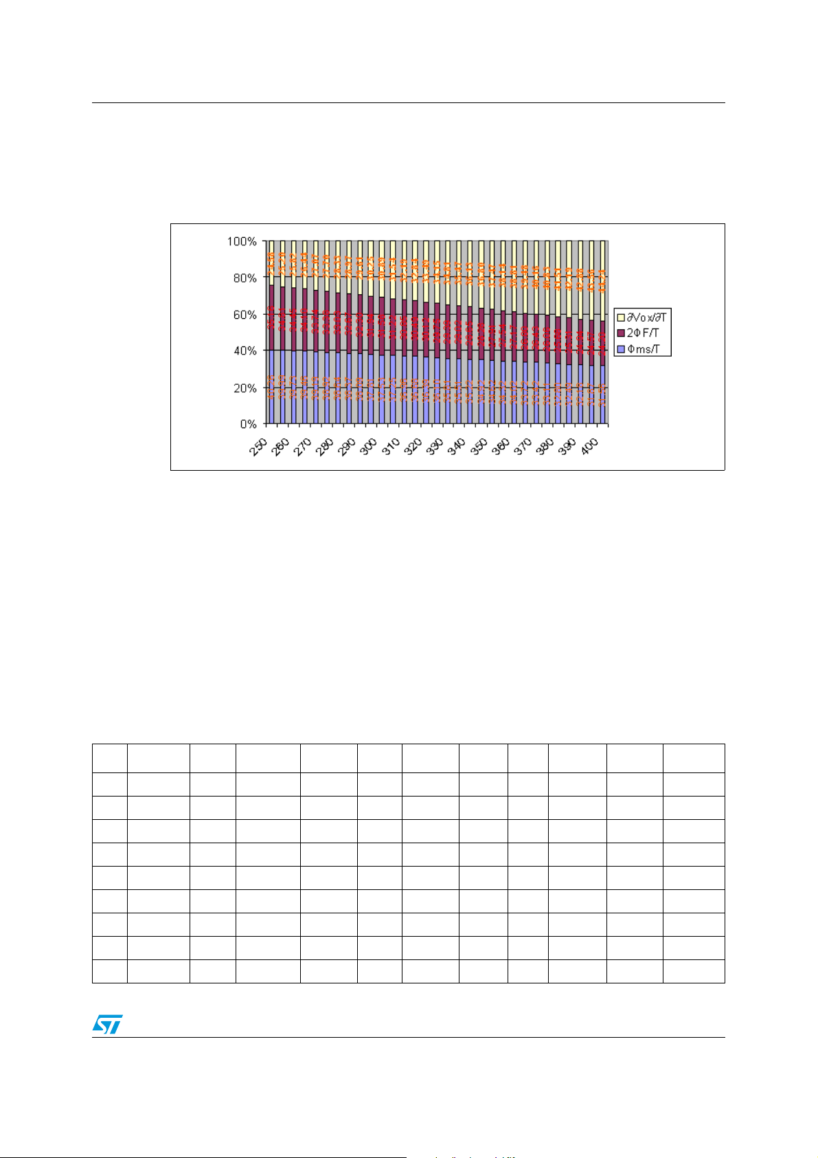
Figure 8. Weight of single term of (Equation 42) on TVTC at different temperatures
In the graph above it is possible see that at a low temperature, the higher weight in the
TVTC formula is established by the parameters Φ
/T and 2ΦF/T. The first term is negative
ms
and makes TVTC negative, while the second term in positive and makes TVTC positive.
When the temperature increases, TVTC increases in absolute value because even if Φ
decreases, 2Φ
/T also decreases and in particular, the weight of ∂Vox/ ∂T increases too.
F
ms
/T
Another real example of threshold voltage and TVTC compared to the theoretical model
implemented is shown below. The low voltage power MOSFET takes into consideration a
device of 55V of breakdown voltage and 6.5mOhm of on resistance (production line
DEVICE1). This device has a gate doping concentration (N
substrate doping concentration peak in the channel (N
) equal to 1e+20cm-3, a
g
) equal to 1e+17cm-3, an oxide
a
thickness of 350Å and a channel length of 0.35µm. The following tab summarizes the main
simulated electrical parameter function of T (T range is 250-400K) and then a graphs
highlights the DEVICE2 measured and simulated data.
Table 2. Main electrical parameter simulated by DEVICE2
TniΦ
250 9.67E+13 -1.043 0.000927 -0.00417 0.447 -0.00076 0.0018 1.76 -0.0015 1.61 -0.0021
255 1.73E+14 -1.038 0.000932 -0.00407 0.443 -0.00076 0.0017 1.75 -0.0015 1.60 -0.0021
260 3.02E+14 -1.033 0.000937 -0.00397 0.439 -0.00077 0.0017 1.74 -0.0015 1.59 -0.0021
265 5.18E+14 -1.029 0.000942 -0.00388 0.436 -0.00077 0.0016 1.74 -0.0015 1.58 -0.0021
270 8.70E+14 -1.024 0.000947 -0.00379 0.432 -0.00077 0.0016 1.73 -0.0015 1.57 -0.0021
275 1.43E+15 -1.019 0.000952 -0.00371 0.428 -0.00077 0.0016 1.72 -0.0016 1.56 -0.0022
280 2.33E+15 -1.015 0.000957 -0.00362 0.424 -0.00078 0.0015 1.71 -0.0016 1.55 -0.0022
285 3.71E+15 -1.010 0.000961 -0.00354 0.420 -0.00078 0.0015 1.71 -0.0016 1.54 -0.0022
290 5.82E+15 -1.005 0.000966 -0.00347 0.416 -0.00078 0.0014 1.70 -0.0016 1.53 -0.0022
∂ms/∂T Φms/T Φ
ms
∂ΦF/∂T ΦF/T V
F
∂VOX/∂TVth∂Vth/∂T
OX
17/30
Page 18

Some considerations on VTH and TVTC equations and real examples AN2386
Table 2. Main electrical parameter simulated by DEVICE2
TniΦ
∂ms/∂T Φms/T Φ
ms
∂ΦF/∂T ΦF/T V
F
∂VOX/∂TVth∂Vth/∂T
OX
295 9.00E+15 -1.000 0.000970 -0.00339 0.412 -0.00078 0.0014 1.69 -0.0016 1.51 -0.0022
300 1.37E+16 -0.995 0.000974 -0.00332 0.408 -0.00078 0.0014 1.68 -0.0016 1.50 -0.0022
305 2.07E+16 -0.990 0.000979 -0.00325 0.404 -0.00079 0.0013 1.67 -0.0016 1.49 -0.0022
310 3.07E+16 -0.985 0.000983 -0.00318 0.400 -0.00079 0.0013 1.67 -0.0016 1.48 -0.0022
315 4.50E+16 -0.980 0.000987 -0.00311 0.397 -0.00079 0.0013 1.66 -0.0017 1.47 -0.0022
320 6.53E+16 -0.976 0.000991 -0.00305 0.393 -0.00079 0.0012 1.65 -0.0017 1.46 -0.0023
325 9.37E+16 -0.971 0.000995 -0.00299 0.389 -0.00080 0.0012 1.64 -0.0017 1.45 -0.0023
330 1.33E+17 -0.966 0.000999 -0.00293 0.385 -0.00080 0.0012 1.63 -0.0017 1.44 -0.0023
335 1.87E+17 -0.961 0.001003 -0.00287 0.381 -0.00080 0.0011 1.62 -0.0017 1.42 -0.0023
340 2.60E+17 -0.956 0.001007 -0.00281 0.377 -0.00080 0.0011 1.61 -0.0017 1.41 -0.0023
345 3.59E+17 -0.951 0.001011 -0.00276 0.373 -0.00080 0.0011 1.61 -0.0017 1.40 -0.0023
350 4.90E+17 -0.945 0.001014 -0.00270 0.369 -0.00080 0.0011 1.60 -0.0017 1.39 -0.0023
355 6.64E+17 -0.940 0.001018 -0.00265 0.365 -0.00081 0.0010 1.59 -0.0018 1.38 -0.0024
360 8.93E+17 -0.935 0.001022 -0.00260 0.361 -0.00081 0.0010 1.58 -0.0018 1.37 -0.0024
365 1.19E+18 -0.930 0.001025 -0.00255 0.356 -0.00081 0.0010 1.57 -0.0018 1.35 -0.0024
370 1.58E+18 -0.925 0.001029 -0.00250 0.352 -0.00081 0.0010 1.56 -0.0018 1.34 -0.0024
375 2.07E+18 -0.920 0.001032 -0.00245 0.348 -0.00081 0.0009 1.55 -0.0018 1.33 -0.0024
380 2.70E+18 -0.915 0.001035 -0.00241 0.344 -0.00082 0.0009 1.54 -0.0018 1.32 -0.0024
385 3.51E+18 -0.910 0.001039 -0.00236 0.340 -0.00082 0.0009 1.53 -0.0018 1.31 -0.0024
390 4.52E+18 -0.904 0.001042 -0.00232 0.336 -0.00082 0.0009 1.53 -0.0019 1.29 -0.0025
395 5.78E+18 -0.899 0.001045 -0.00228 0.332 -0.00082 0.0008 1.52 -0.0019 1.28 -0.0025
400 7.36E+18 -0.894 0.001049 -0.00223 0.328 -0.00082 0.0008 1.51 -0.0019 1.27 -0.0025
Figure 9. DEVICE2 VTH - comparison between simulated and measured data
18/30
Page 19
AN2386 Some considerations on VTH and TVTC equations and real examples
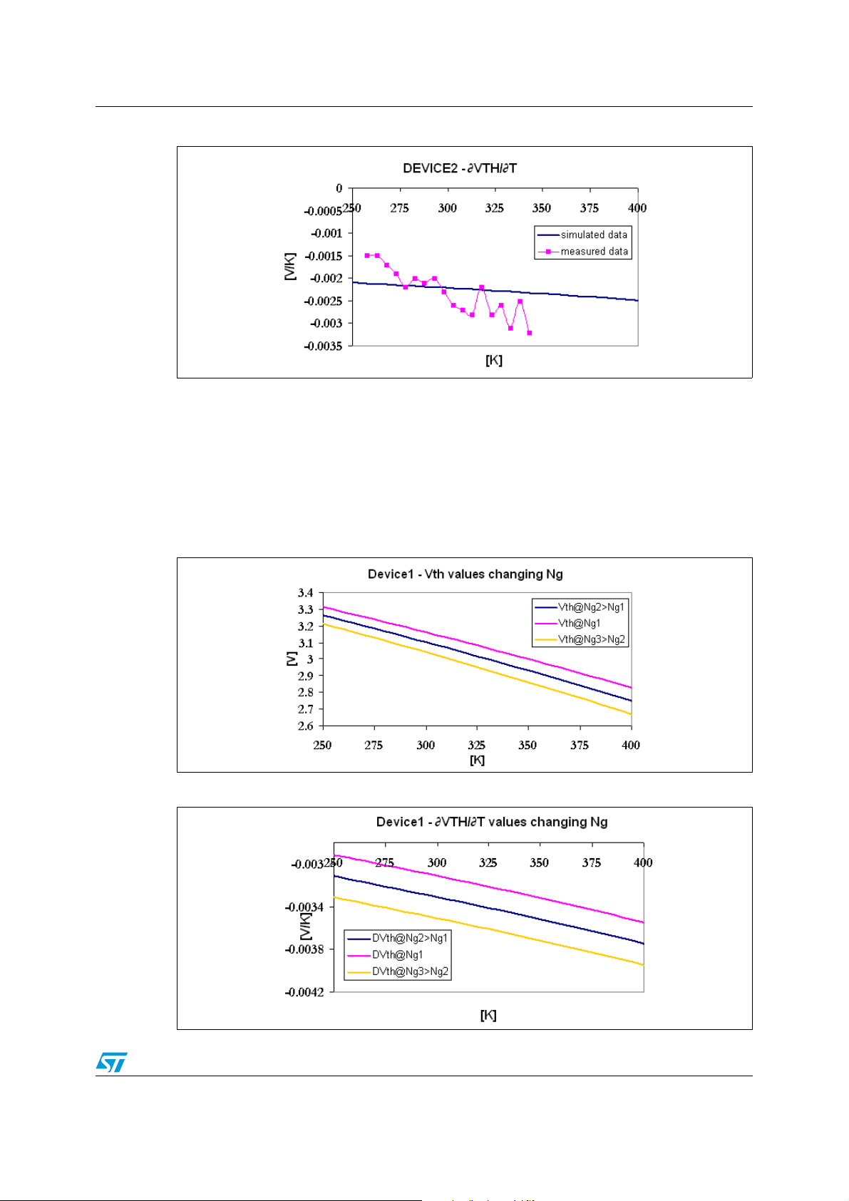
Figure 10. DEVICE2 TVTC - comparison between simulated and measured data
Also in this new case, the data simulated and measured are quite close to each other. In this
case, for DEVICE2, the threshold voltage is around 1.5V and TVTC is around 2mV/K at
ambient temperature.
Now it is possible to consider the DEVICE1 device and simulate the V
behavior changing N
, Na and tox respectively.
g
and TVTC thermal
TH
At the beginning, the thermal behavior increasing and decreasing the gate doping
concentration is simulated (see Figure 11. and Figure 12.).
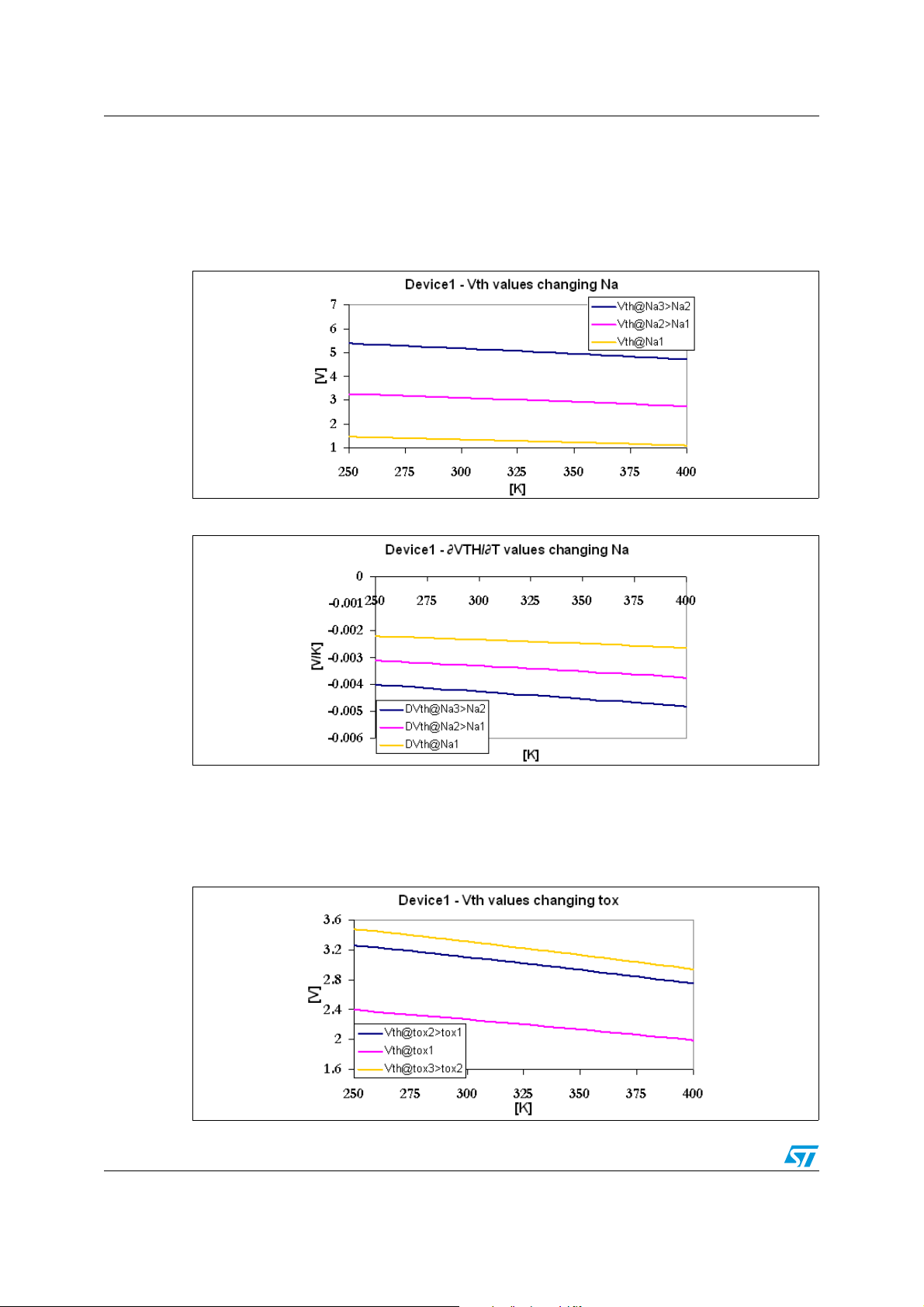
Figure 11. DEVICE1 V
simulated data - comparison between different N
TH
g
Figure 12. DEVICE1 TVTC simulated data - comparison between different N
g
19/30
Page 20
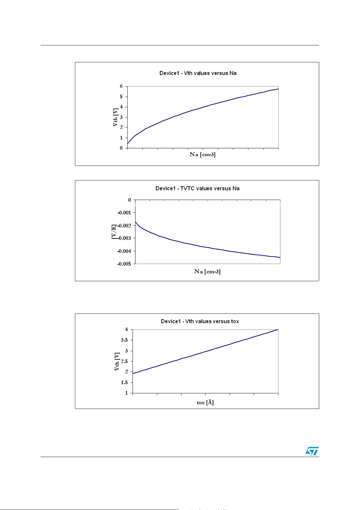
Some considerations on VTH and TVTC equations and real examples AN2386
When the gate concentration doping increases from 1e+20cm-3 to 1e+21cm-3 the threshold
voltage decreases its value, while, TVTC increases in absolute value and vice versa,
decreasing the gate concentration doping from 1e+20cm
-3
to 1e+19cm-3. Now, the thermal
behavior increasing and decreasing the substrate doping concentration is simulated (see
Figure 13. and Figure 14.).
Figure 13. DEVICE1 V
simulated data - comparison between different N
TH
a
Figure 14. DEVICE1 TVTC simulated data - comparison between different N
a
When the substrate concentration doping increases from 2e+17cm-3 to 5e+17cm-3 the
threshold voltage increases its value and also TVTC increases in absolute value and vice
versa, decreasing the substrate concentration doping from 2e+17cm
the case of different thickness oxide will be studied (see Figure 15. and Figure 16.).
Figure 15. DEVICE1 V
20/30
simulated data - comparison between different t
TH
-3
to 5e+16cm-3. Now,
ox
Page 21
AN2386 Some considerations on VTH and TVTC equations and real examples
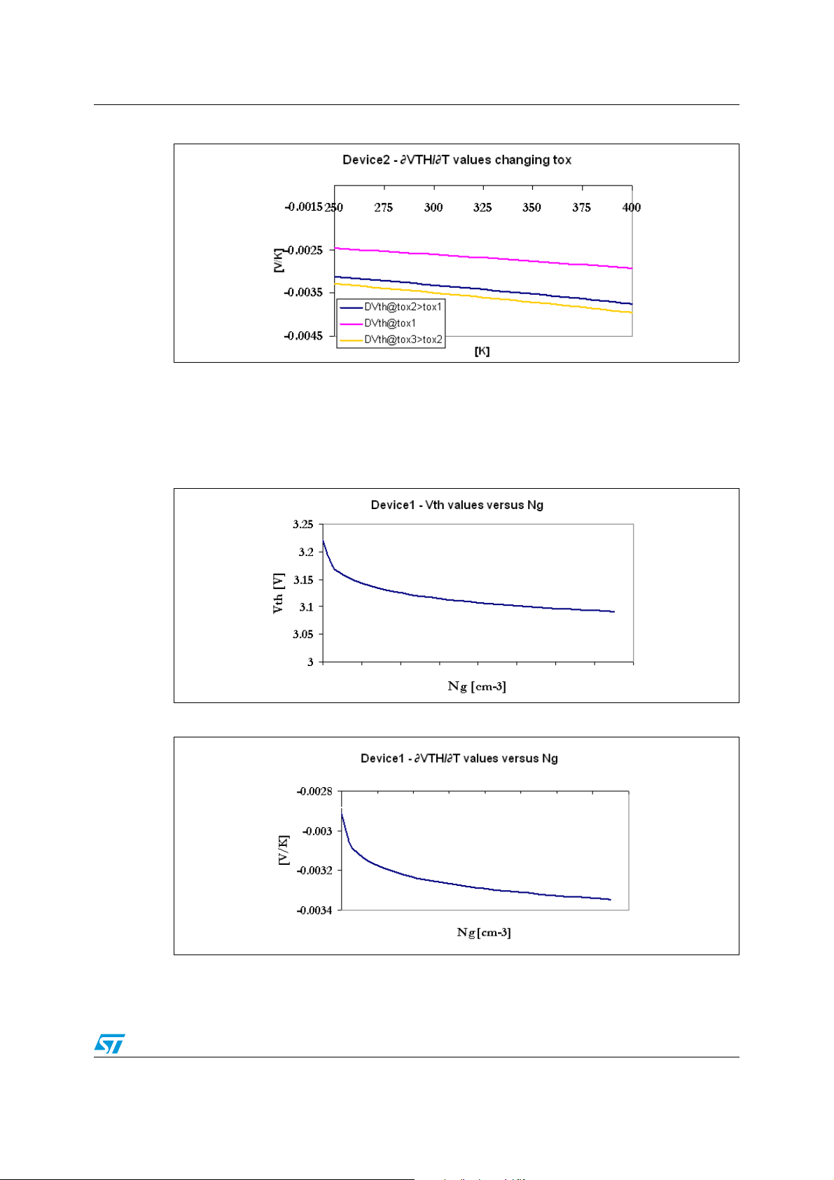
Figure 16. DEVICE1 TVTC simulated data - comparison between different t
ox
When the oxide thickness increases from 470Å to 500Å, the threshold voltage increases its
value and also TVTC increases in absolute value and vice versa, decreases the thickness
oxide from 470Å to 350Å. Now, it is possible simulate V
temperature is fixed to 300K and the gate doping concentration changes in the range of
1e+18-1.5e+20cm
Figure 17. DEVICE1 V
-3
(see Figure 17. and Figure 18.).
simulated data - fixing T and acting on N
TH
and TVTC supposing that the
TH
g
Figure 18. DEVICE1 TVTC simulated data - fixing T and acting on N
g
The graph in Figure 19. and Figure 20. show VTH and TVTC trend fixing the temperature to
300K and changing N
in the range of 1e+16-6.1e+17cm-3.
a
21/30
Page 22
Some considerations on VTH and TVTC equations and real examples AN2386
Figure 19. DEVICE1 VTH simulated data - fixing T and acting on N
a
Figure 20. DEVICE1 TVTC simulated data - fixing T and acting on N
a
The graph inFigure 21. and Figure 22. shows VTH and TVTC trend fixing the temperature to
300K and changing t
Figure 21. DEVICE1 V
22/30
in the range of 300-600Å.
ox
simulated data - fixing T and acting on t
TH
ox
Page 23
AN2386 Some considerations on VTH and TVTC equations and real examples
Figure 22. DEVICE1 TVTC simulated data - fixing T and acting on t
ox
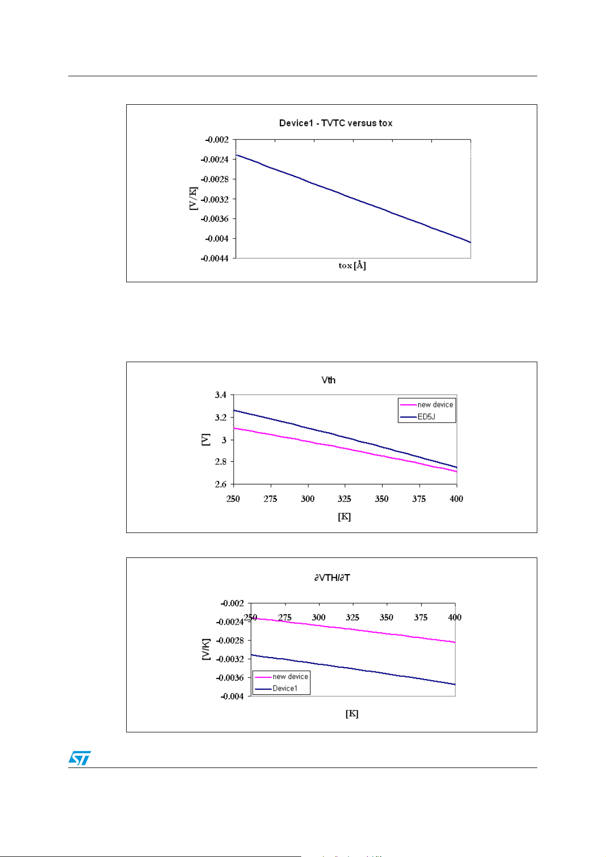
The next graphs show the simulated data of VTH and TVTC considering DEVICE1 and a
hypothetical new device with standard threshold voltage and minimized TVTC. This device
is obtained changing on N
equal to 1e+18cm
Figure 23. V
-3
, Na is equal to 3e+17cm-3 and tox is equal to 350Å.
simulated data - comparison between DEVICE1 and the new device
TH
, Ng and tox together. For example, this new device has Ng is
a
Figure 24. TVTC simulated data - comparison between DEVICE1 and the new device
23/30
Page 24
Some considerations on VTH and TVTC equations and real examples AN2386
It is possible see that by rearranging Ng, Na and tox the threshold voltage remains fixed and
TVTC decreases in absolute value.
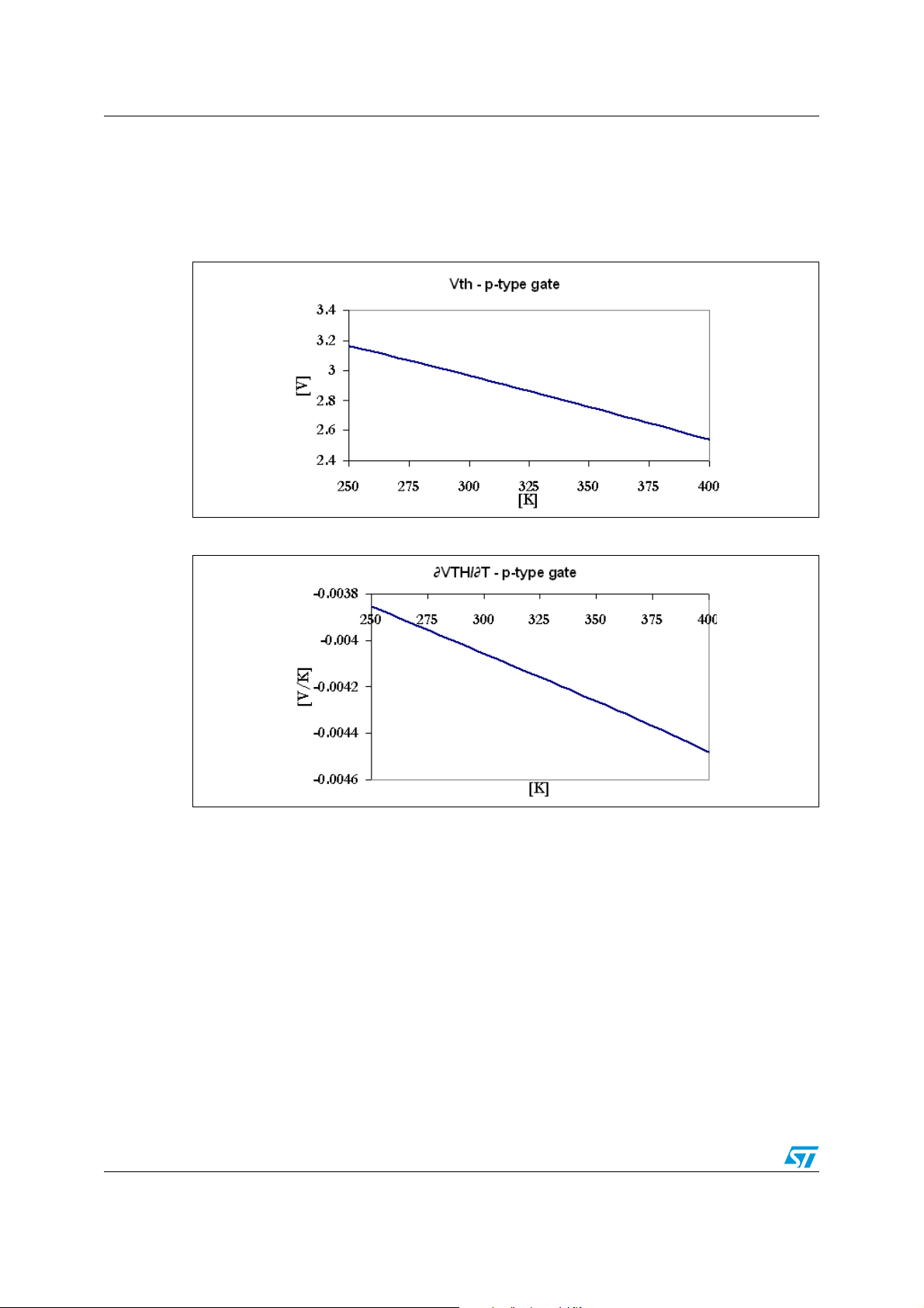
Finally, the following graphs highlight the V
doped MOS with N
Figure 25. V
equal to 1e+21cm-3, Na is equal to 3e+16cm-3 and tox is equal to 470Å.
g
simulated data considering a p-gate doped MOS
TH
and TVTC trend simulates a p-type gate
TH
Figure 26. TVTC simulated data considering a p-gate doped MOS
The only difference with the n-type doped gate is that increasing the gate doping
concentration, TVTC decreases in absolute value instead of increasing.
24/30
Page 25
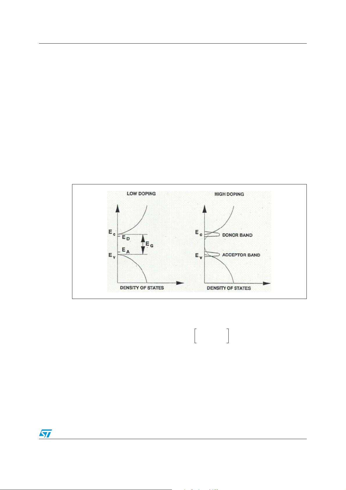
AN2386 Case of DEVICE3
3 Case of DEVICE3
The device DEVICE3 has similar characteristics of DEVICE1 in terms of tox (470Å), gate
doping (1e+20cm
-3
), silicon doping (2.4e+17cm-3) and breakdown voltage 55V. The main
difference between the two devices consists in the channel length (0.8µm) and the source
doping thermal process activation; DEVICE3 perform a form while DEVICE1 an RTA
thermal process.
The only difference on the length channels between the two devices should not have an
effect on the threshold voltage and TVTC. Instead, the different source thermal process
doping activation could bring a variation on the TVTC because the net charge peak
concentration in the channel near the source well is higher in the silicon processed in the
form compared to the RTA one. In fact, when the net charge concentration in the silicon
overcomes typically 1e+17[cm
-3
], a band-gap narrowing effect occurs (see Figure 27.)
because new impurity band states are created inside the forbidden silicon band near the
conduction and valence edges.
Figure 27. Energy band diagram at low and high doping concentration
In order to consider this effect the Slotboom-De Graaf model is used.
Equation 46
1
-- -
2
0.5+
Eg∆ b1T
=
∆Eg is the band-gap narrowing value; N
N
T
----------- -
+ln
17
10
(expressed in cm-3) is the net charge
T
2
-----
ln
concentration (the sum of acceptor and donor doping elements concentration).
The net charge concentration is not easy to establish so, in order to fit the real data, a net
charge concentration of 3.5e+17cm
-3
was considered for DEVICE3.
The real data on DEVICE3 using RTA process are shown in the following figures where are
compared to the simulated and the data of the device using the form process.
25/30
Page 26

Case of DEVICE3 AN2386
Figure 28. DEVICE3 VTH - comparison between simulated and measured data
Figure 29. DEVICE3 TVTC - comparison between simulated and measured data
Also in this case, the simulated data and the measured data are close to each other.
26/30
Page 27

AN2386 Conclusions
4 Conclusions
This paper has studied the effect of the temperature on the MOSFET threshold voltage and
its thermal coefficient. In particular, a mathematical model for both parameters was
achieved and a comparison with real measurement was performed considering three low
voltage power MOSFET devices by ST; DEVICE1, DEVICE2 and DEVICE3. The simulated
and real data obtained for all the devices under test are quite close and, thus confirming the
validation of the theory.
The model has highlighted that, in order to decreases in absolute value TVTC to avoid
thermal run-away of the device, the thickness oxide, silicon and the gate doping
concentration must be decreased. However, minimizing TVTC and obtaining a standard
threshold voltage device can't be done by decreasing the three parameters together, they
must be rearranged as in the example shown in Figure 23. and Figure 24. of this article.
Another important result shown in this paper regards the example of the device DEVICE3.
In this case, the higher total charge concentration in the channel involves a band-gap
narrowing that increases in absolute value TVTC and makes the device more thermally
instable.
27/30
Page 28

References AN2386
5 References
● Introduction on semiconductor materials
– Au. Tyagi - Ed. Wiley&Sons
● Atlas User's Manual Vol.I - February 2000
– Silvaco International
● Mutual Compensation of Mobility and Threshold Voltage Temperature Effects with
Applications in CMOS Circuit
– Au. I.M. Filanovsky A. Allam Ed. IEEE Vol. 48 No. 7, July 2001
28/30
Page 29

AN2386 Revision history
6 Revision history
Table 3. Revision history
Date Revision Changes
13-Jun-2006 1 Initial release.
29/30
Page 30

AN2386
Please Read Carefully:
Information in this document is provided solely in connection with ST products. STMicroelectronics NV and its subsidiaries (“ST”) reserve the
right to make changes, corrections, modifications or improvements, to this document, and the products and services described herein at any
time, without notice.
All ST products are sold pursuant to ST’s terms and conditions of sale.
Purchasers are solely responsible for the choice, selection and use of the ST products and services described herein, and ST assumes no
liability whatsoever relating to the choice, selection or use of the ST products and services described herein.
No license, express or implied, by estoppel or otherwise, to any intellectual property rights is granted under this document. If any part of this
document refers to any third party products or services it shall not be deemed a license grant by ST for the use of such third party products
or services, or any intellectual property contained therein or considered as a warranty covering the use in any manner whatsoever of such
third party products or services or any intellectual property contained therein.
UNLESS OTHERWISE SET FORTH IN ST’S TERMS AND CONDITIONS OF SALE ST DISCLAIMS ANY EXPRESS OR IMPLIED
WARRANTY WITH RESPECT TO THE USE AND/OR SALE OF ST PRODUCTS INCLUDING WITHOUT LIMITATION IMPLIED
WARRANTIES OF MERCHANTABILITY, FITNESS FOR A PARTICULAR PURPOSE (AND THEIR EQUIVALENTS UNDER THE LAWS
OF ANY JURISDICTION), OR INFRINGEMENT OF ANY PATENT, COPYRIGHT OR OTHER INTELLECTUAL PROPERTY RIGHT.
UNLESS EXPRESSLY APPROVED IN WRITING BY AN AUTHORIZE REPRESENTATIVE OF ST, ST PRODUCTS ARE NOT DESIGNED,
AUTHORIZED OR WARRANTED FOR USE IN MILITARY, AIR CRAFT, SPACE, LIFE SAVING, OR LIFE SUSTAINING APPLICATIONS,
NOR IN PRODUCTS OR SYSTEMS, WHERE FAILURE OR MALFUNCTION MAY RESULT IN PERSONAL INJURY, DEATH, OR
SEVERE PROPERTY OR ENVIRONMENTAL DAMAGE.
Resale of ST products with provisions different from the statements and/or technical features set forth in this document shall immediately void
any warranty granted by ST for the ST product or service described herein and shall not create or extend in any manner whatsoever, any
liability of ST.
ST and the ST logo are trademarks or registered trademarks of ST in various countries.
Information in this document supersedes and replaces all information previously supplied.
The ST logo is a registered trademark of STMicroelectronics. All other names are the property of their respective owners.
© 2006 STMicroelectronics - All rights reserved
STMicroelectronics group of companies
Australia - Belgium - Brazil - Canada - China - Czech Republic - Finland - France - Germany - Hong Kong - India - Israel - Italy - Japan -
Malaysia - Malta - Morocco - Singapore - Spain - Sweden - Switzerland - United Kingdom - United States of America
www.st.com
30/30
 Loading...