

Page 1

AN2377
Application note
Using the STM1403/1404 security supervisors
to clear external SRAM
Introduction
The STM1403/1404 is a family of low power intrusion (tamper) detection security
supervisors for the Point of Sale (POS) terminal market. They enable manufacturers to meet
security standards such as FIPS-140 (NIST, US Dept. of Commerce), EMV Co, ISO, ZKA
(Germany) and Visa PED. Until recently, many of these intrusion detection functions were
implemented by using several discrete devices. The STM1403/1404 integrates all these
functions into a small profile security-friendly QFN package. The STM1403/1404 meets
most price, performance and board space objectives while ensuring customers are able to
meet current and future security certification requirements for physical and environmental
tamper detection.
June 2006 Rev 1 1/14
www.st.com
Page 2

Contents AN2377
Contents
1 Targeted applications . . . . . . . . . . . . . . . . . . . . . . . . . . . . . . . . . . . . . . . . 5
1.1 High security module (HSM) . . . . . . . . . . . . . . . . . . . . . . . . . . . . . . . . . . . 5
1.2 Security levels . . . . . . . . . . . . . . . . . . . . . . . . . . . . . . . . . . . . . . . . . . . . . . 5
1.3 STM1403 integrated functions . . . . . . . . . . . . . . . . . . . . . . . . . . . . . . . . . . 6
1.4 STM1404 for security level 4 . . . . . . . . . . . . . . . . . . . . . . . . . . . . . . . . . . . 6
2 How it works . . . . . . . . . . . . . . . . . . . . . . . . . . . . . . . . . . . . . . . . . . . . . . . 7
2.1 Physical tamper . . . . . . . . . . . . . . . . . . . . . . . . . . . . . . . . . . . . . . . . . . . . . 7
2.2 Over/under voltage detection . . . . . . . . . . . . . . . . . . . . . . . . . . . . . . . . . . . 7
2.3 Over/under temperature detection (STM1404 only) . . . . . . . . . . . . . . . . . . 7
2.4 Clearing external memory . . . . . . . . . . . . . . . . . . . . . . . . . . . . . . . . . . . . . 7
2.5 Clearing the external memory using a negative charge pump (STM140xB) 8
3 Efficiency results . . . . . . . . . . . . . . . . . . . . . . . . . . . . . . . . . . . . . . . . . . . 10
4 Conclusion . . . . . . . . . . . . . . . . . . . . . . . . . . . . . . . . . . . . . . . . . . . . . . . . 12
5 Revision history . . . . . . . . . . . . . . . . . . . . . . . . . . . . . . . . . . . . . . . . . . . 13
2/14
Page 3

AN2377 List of figures
List of figures
Figure 1. Federal information processing standard 140 . . . . . . . . . . . . . . . . . . . . . . . . . . . . . . . . . . . 5
Figure 2. Circuit connection to drive SRAM V
Figure 3. Circuit connection when using negative charge pump (STM140xB) . . . . . . . . . . . . . . . . . . 9
to ground (STM140xC) . . . . . . . . . . . . . . . . . . . . . . 8
CC
3/14
Page 4

List of tables AN2377
List of tables
Table 1. STM1403/1404 V
Table 2. 1 Mb SRAM clear characterization results - Vendor1 . . . . . . . . . . . . . . . . . . . . . . . . . . . . . 10
Table 4. 1 Mb SRAM clear characterization results - Vendor3 . . . . . . . . . . . . . . . . . . . . . . . . . . . . . 11
Table 3. 1 Mb SRAM clear characterization results - Vendor2 . . . . . . . . . . . . . . . . . . . . . . . . . . . . . 11
Table 5. Revision history . . . . . . . . . . . . . . . . . . . . . . . . . . . . . . . . . . . . . . . . . . . . . . . . . . . . . . . . . 13
status during alarm . . . . . . . . . . . . . . . . . . . . . . . . . . . . . . . . . . . . . . 7
OUT
4/14
Page 5
AN2377 Targeted applications
1 Targeted applications
The STM1403/1404 family can be used in the High Security Module (HSM) of a Point of
Sale system such as: POS terminals, PCs with cash drawers, standalone credit
authorization / debit card terminals, electronic cash registers, vending machines, standalone
check readers and signature capture devices.
1.1 High security module (HSM)
The STM1403/1404 may be incorporated into the HSM which also includes the
cryptographic module with the crypto keys stored in secure SRAM. The STM1403/1404
devices integrate most, if not all, of the key functions necessary to continuously monitor
physical tamper inputs, supply voltages (primary Vcc and secondary battery back-up) and
ambient temperature (STM1404 only).
When an intrusion is detected, an alarm is issued by the STM1403/1404 device. Once the
alarm is received by the system it can immediately initiate a process to "zeroize" the
cryptographic keys in volatile SRAM to prevent the intruder from gaining access to them.
The HSM is thus rendered non-functional, until shipped back to the factory for diagnostic
tests and re-coding.
1.2 Security levels
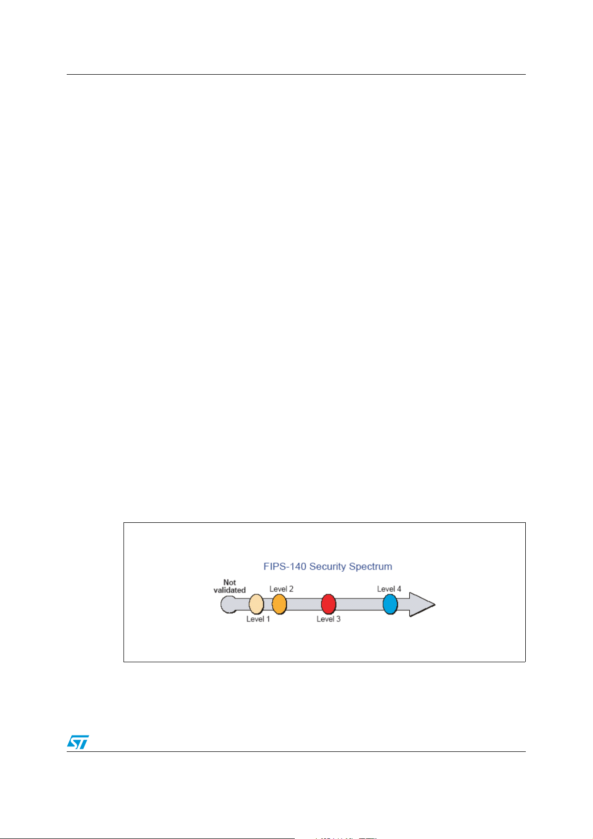
There are different levels of security certification depending on the system application. As
an example, the FEDERAL INFORMATION PROCESSING STANDARDS (FIPS-140)
publication provides a standard used by Federal organizations when these organizations
specify that cryptographic-based security systems are necessary to provide protection for
sensitive data. There are many other country specific and industry specific standards that
POS system vendors are required to meet.
The STM1403/1404 family has been defined to meet these standards for physical and
environmental tamper detection.
Figure 1. Federal information processing standard 140
5/14
Page 6

Targeted applications AN2377
1.3 STM1403 integrated functions
The STM1403 device is targeted at Security Level 3 and lower. It has the following functions
integrated: STM704 battery switchover supervisor; Physical tamper detect/alarm functions;
Over/under operating voltage alarm; Battery low voltage detect function; and an optional
voltage reference (Vref) out of 1.237V.
1.4 STM1404 for security level 4
There is also the 100% pin-compatible STM1404, a functional superset of the STM1403,
targeted at highest security level 4. In addition to the functionality of STM1403, it has
several options of factory programmed over/under temperature alarms.
6/14
Page 7

AN2377 How it works
2 How it works
2.1 Physical tamper
The STM1403/1404 device provides four independent tamper input pins, TP1 through TP4,
that can be used to monitor four separate signals. These tamper input pins can be used to
indicate that a tamper event has occurred by either the opening or closing of a switch,
forcing the pin to its tampered state (a high level for pins TP
and TP
).
3
2.2 Over/under voltage detection
and TP4, or low level for TP1
2
When the internal voltage (VINT; where V
high voltage limit (V
) or drops below the low voltage limit (VLV), an alarm is generated.
HV
can be V
INT
or VCC), either goes above the
BAT
2.3 Over/under temperature detection (STM1404 only)
When the die temperature (TA), either goes above the high temperature limit (TH) or drops
below the low temperature limit (T
), an alarm is generated.
L
After any alarm condition occurs, the open drain Security Alarm Output (/SAL) will be forced
low.
2.4 Clearing external memory
The STM1403/1404 can easily be configured to clear external, battery-backed SRAM. One
way to clear or corrupt the external memory, is to force V
removes power from the volatile SRAM, allowing the memory array to return to its default
state, effectively clearing the sensitive data contained in the memory array. The STM140xC
is designed specifically for this purpose (See Table 1.). When any alarm condition occurs,
forcing the /SAL pin low, the V
be forced low, driving the V
pin which supplies power to the external SRAM, will also
OUT
pin of the SRAM to Ground. Figure 2. shows the circuit
CC
connection. The voltage regulator should also be disabled to avoid powering the SRAM
through the input protection of one of its address or control pins.
of the SRAM to Ground. This
CC
Table 1. STM1403/1404 V
Option V
STM140xA ON Remains powered-up
STM140xB High-Z For use with negative charge pump
STM140xC Ground Basic approach to clear SRAM
status during alarm
OUT
Status during alarm Affect on external SRAM
OUT
7/14
Page 8

How it works AN2377
Figure 2. Circuit connection to drive SRAM VCC to ground (STM140xC)
2.5 Clearing the external memory using a negative charge pump (STM140xB)
However, some SRAMs require a significant amount of time for the memory to be corrupted
if V
is simply grounded. To corrupt the memory in a shorter period of time, the user can
CC
take V
protection diode turns on forcing any internal capacitive nodes to be discharged, quickly
corrupting the memory.
Therefore, in order to rapidly corrupt the external volatile SRAM, a negative charge pump
device should be used with the STM140xB to drive V
during the tamper condition. Figure 3. shows how to connect this circuit. When using the
STM140xB with the charge pump device, the user must also provide a standard hex inverter
and an N-channel MOSFET to isolate the V
the charge pump during normal operation. During normal operation the active low / SAL
signal will be high, disabling the charge pump. While disabled, the output of most charge
pumps will be forced to Ground. In order to allow proper operation of the SRAM, the
MOSFET must be "off" to isolate V
During a tamper condition, the /SAL output will be forced low, causing the corresponding
hex inverter outputs to go high. One signal will control the inhibit pin of the DC regulator,
putting the regulator in standby mode, removing power from the circuit. A second signal will
turn ON the N-channel MOSFET, connecting the output of the charge pump with the V
of the SRAM. A third signal will enable the charge pump generating a negative voltage on
the V
function of the SRAM used, and the magnitude and duration of the negative voltage applied.
This should be characterized in the application by the user.
of the SRAM to a negative voltage. By taking VCC to a negative voltage, the input
CC
of the SRAM to a negative voltage
CC
of the STM140xB from the output (OUT) of
OUT
of the SRAM from the charge pump output.
CC
pin of the SRAM, causing data corruption. Clearing the SRAM data is primarily a
CC
CC
pin
It is typically recommended that low ESR capacitors be used with the charge pump to
reduce noise and ripple. A small capacitance value delivers less charge per clock cycle to
the output, resulting in lower output ripple and also a reduction in the maximum I
8/14
OUT
Page 9

AN2377 How it works
capability. Therefore, a ceramic capacitor is initially recommended with a value in the range
of 0.022µF or less.
Figure 3. Circuit connection when using negative charge pump (STM140xB)
9/14
Page 10

Efficiency results AN2377
3 Efficiency results
Depending on the process technology used to manufacture of the external SRAM, clearing
the memory may require varying durations of negative potential on the V
At STMicroelectronics, we have evaluated several different SRAMs with different densities
and found that we were able to corrupt the memory with certain minimum duration (1
second) negative pulse widths (see Table 2., Table 3. and Table 4.).
Table 2. 1 Mb SRAM clear characterization results - Vendor1
Vendor Vcc Temp Pulse width Memory clear Comments
CC
pin.
Vendor1
Vss
-1V Undershoot 1.6 msec No Partial corruption
-1V Undershoot 4msec Yes Corrupted with random data
Vss
Vss 10sec Yes Corrupted with random data
-1V Undershoot 10msec Yes Corrupted with random data
Vss
Vss 55sec No
Vss 70sec Yes Corrupted with random data
-1V Undershoot 1.0 sec No Partial corruption
-1V Undershoot 1.3 sec No Partial corruption
-1V Undershoot 1.6 sec Yes Corrupted with random data
-2V Undershoot 8 msec No Partial corruption
-2V Undershoot 40 msec Yes Corrupted with random data
-1V Undershoot
-1V Undershoot 16sec No
-1V Undershoot 20 sec Yes Corrupted with random data
-2V Undershoot 40 sec No Partial corruption
-2V Undershoot 80 msec Yes Corrupted with random data
85°C
25°C
0°C
-40°C
1 sec Yes Corrupted with random data
8sec No
35sec No
8 sec No
10/14
Page 11

AN2377 Efficiency results
Table 3. 1 Mb SRAM clear characterization results - Vendor2
Vendor Vcc Temp Pulse width Memory clear Comments
Vendor2
-1V Undershoot
-1V Undershoot 80msec Yes Corrupted with random data
-1V Undershoot 25°C 10msec Yes Corrupted with random data
-1V Undershoot
-1V Undershoot 1.6 sec Yes Corrupted with random data
-2V Undershoot 8 msec No Partial corruption
-2V Undershoot 40 msec Yes Corrupted with random data
-2V Undershoot
-2V Undershoot 800 msec No
-2V Undershoot 1.6 sec Yes Corrupted with random data
85°C
0°C
-40°C
8msec No
1.3 sec No Partial corruption
200 msec No
Table 4. 1 Mb SRAM clear characterization results - Vendor3
Vendor Vcc Temp Pulse width Memory clear Comments
-1V Undershoot 85°C 4 msec Yes Corrupted with random data
-1V Undershoot
-1V Undershoot 40 msec No
25°C
-1V Undershoot 80 msec No
-1V Undershoot 160 msec Yes Corrupted with random data
-1V Undershoot
16 msec No
800 msec No Partial corruption
-1V Undershoot 1.0 sec No Partial corruption
Vendor3
-1V Undershoot 2.0 sec Yes Corrupted with random data
-2V Undershoot 400 msec No
-2V Undershoot 800 msec No Partial corruption
-2V Undershoot 1 sec Yes Corrupted with random data
-1V Undershoot
-1V Undershoot 8 sec No
-1V Undershoot 20 sec Yes Corrupted with random data
-2V Undershoot 1.6 sec No
-2V Undershoot 4 sec No
-2V Undershoot 10 sec Yes Corrupted with random data
0°C
4 sec No
-40°C
Note: The data above was taken to evaluate various SRAMs to determine the length of time
required to clear the data by grounding or forcing a negative voltage on the Vcc supply pin.
This data indicates that the time is a function of temperature, voltage and manufacturer (and
may also vary by revision). This data was taken on a very limited sample size, and should
not be considered conclusive. No data was taken to evaluate the long-term reliability impact
on the SRAM as a result of the negative voltages.
11/14
Page 12

Conclusion AN2377
4 Conclusion
With the increasing frequency of credit card fraud and identity theft in applications like ATM
machines or POS terminals, ST is leading the way in protecting this sensitive data with its
new line of security supervisors. When this sensitive data is stored in external volatile
memory the STM1403/1404 solution can provide early detection when these devices have
been tampered with and also clear the RAM before the intruder can access this data.
12/14
Page 13

AN2377 Revision history
5 Revision history
Table 5. Revision history
Date Revision Changes
29-Jun-2006 1 Initial release.
13/14
Page 14

AN2377
Please Read Carefully:
Information in this document is provided solely in connection with ST products. STMicroelectronics NV and its subsidiaries (“ST”) reserve the
right to make changes, corrections, modifications or improvements, to this document, and the products and services described herein at any
time, without notice.
All ST products are sold pursuant to ST’s terms and conditions of sale.
Purchasers are solely responsible for the choice, selection and use of the ST products and services described herein, and ST assumes no
liability whatsoever relating to the choice, selection or use of the ST products and services described herein.
No license, express or implied, by estoppel or otherwise, to any intellectual property rights is granted under this document. If any part of this
document refers to any third party products or services it shall not be deemed a license grant by ST for the use of such third party products
or services, or any intellectual property contained therein or considered as a warranty covering the use in any manner whatsoever of such
third party products or services or any intellectual property contained therein.
UNLESS OTHERWISE SET FORTH IN ST’S TERMS AND CONDITIONS OF SALE ST DISCLAIMS ANY EXPRESS OR IMPLIED
WARRANTY WITH RESPECT TO THE USE AND/OR SALE OF ST PRODUCTS INCLUDING WITHOUT LIMITATION IMPLIED
WARRANTIES OF MERCHANTABILITY, FITNESS FOR A PARTICULAR PURPOSE (AND THEIR EQUIVALENTS UNDER THE LAWS
OF ANY JURISDICTION), OR INFRINGEMENT OF ANY PATENT, COPYRIGHT OR OTHER INTELLECTUAL PROPERTY RIGHT.
UNLESS EXPRESSLY APPROVED IN WRITING BY AN AUTHORIZE REPRESENTATIVE OF ST, ST PRODUCTS ARE NOT DESIGNED,
AUTHORIZED OR WARRANTED FOR USE IN MILITARY, AIR CRAFT, SPACE, LIFE SAVING, OR LIFE SUSTAINING APPLICATIONS,
NOR IN PRODUCTS OR SYSTEMS, WHERE FAILURE OR MALFUNCTION MAY RESULT IN PERSONAL INJURY, DEATH, OR
SEVERE PROPERTY OR ENVIRONMENTAL DAMAGE.
Resale of ST products with provisions different from the statements and/or technical features set forth in this document shall immediately void
any warranty granted by ST for the ST product or service described herein and shall not create or extend in any manner whatsoever, any
liability of ST.
ST and the ST logo are trademarks or registered trademarks of ST in various countries.
Information in this document supersedes and replaces all information previously supplied.
The ST logo is a registered trademark of STMicroelectronics. All other names are the property of their respective owners.
© 2006 STMicroelectronics - All rights reserved
STMicroelectronics group of companies
Australia - Belgium - Brazil - Canada - China - Czech Republic - Finland - France - Germany - Hong Kong - India - Israel - Italy - Japan -
Malaysia - Malta - Morocco - Singapore - Spain - Sweden - Switzerland - United Kingdom - United States of America
www.st.com
14/14
 Loading...