

AN2366
Application note
Guidelines for migrating ST72F324 or ST72324 (ROM)
applications to ST72F324B or ST72324B (ROM)
Introduction
This application note provides information on using ST72F324B, ST72324B (ROM)
microcontroller devices in applications originally designed for the ST72F324 and ST72324
(ROM) series.
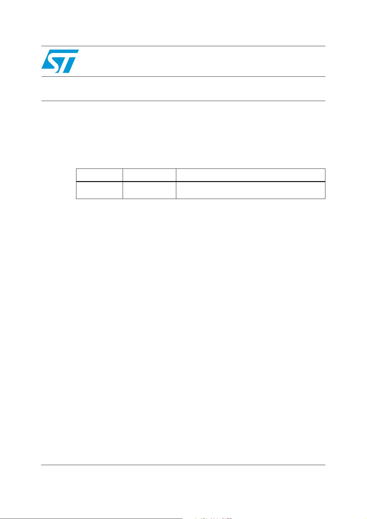
Table 1. Migration cross-reference table
From To Description
ST72F324,
ST72324
ST72F324B,
ST72324B
8K to 32K program memory, 32-pin and 42-/44-pin
July 2009 Doc ID 12345 Rev 2 1/8
www.st.com

Contents AN2366
Contents
1 ST72F324 migration: feature overview . . . . . . . . . . . . . . . . . . . . . . . . . . 3
2 Feature compatibility . . . . . . . . . . . . . . . . . . . . . . . . . . . . . . . . . . . . . . . . 4
2.1 VDD Rise time . . . . . . . . . . . . . . . . . . . . . . . . . . . . . . . . . . . . . . . . . . . . . . 4
2.2 Asynchronous RESET
2.3 Oscillator pad . . . . . . . . . . . . . . . . . . . . . . . . . . . . . . . . . . . . . . . . . . . . . . . 4
pin . . . . . . . . . . . . . . . . . . . . . . . . . . . . . . . . . . . . . 4
3 Performance improvements . . . . . . . . . . . . . . . . . . . . . . . . . . . . . . . . . . . 5
4 Limitations summary . . . . . . . . . . . . . . . . . . . . . . . . . . . . . . . . . . . . . . . . 6
5 Revision history . . . . . . . . . . . . . . . . . . . . . . . . . . . . . . . . . . . . . . . . . . . . 7
2/8 Doc ID 12345 Rev 2
AN2366 ST72F324 migration: feature overview
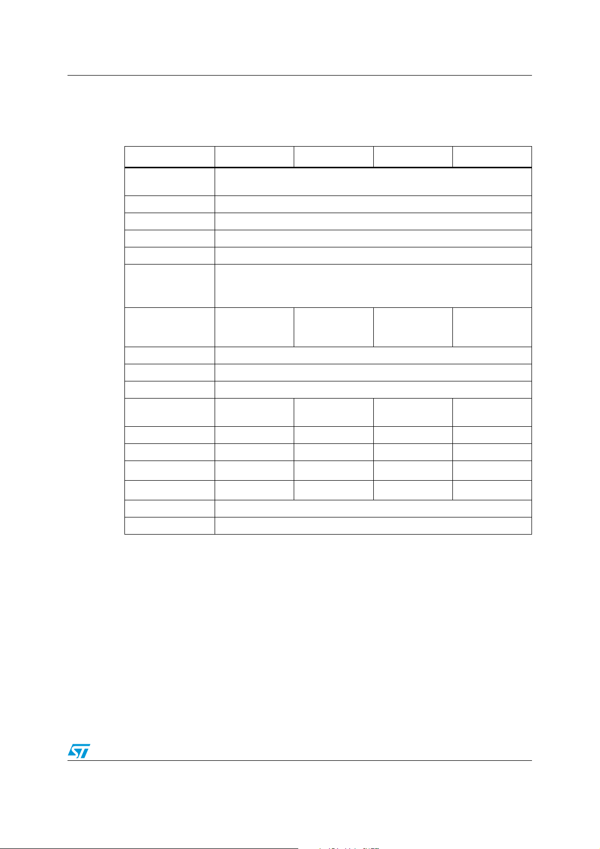
1 ST72F324 migration: feature overview
Table 2. Feature overview
Feature
Package
Program memory 8K to 32K
RAM 384 bytes to 1 Kbyte
Operating supply 3.8V to 5.5V
Register map 128 bytes
I/Os
Power saving modes
Nested interrupts Yes
(1)
ST72F324 ST72324 ROM ST72F324B ST72324B ROM
(2)
TQFP44 (10x10) / SDIP42
/
TQFP32 (7x7) / SDIP32
32/24 Multifunction bidirectional lines
22/17 Alternate function lines
12/10 High sink outputs
Slow / Wait /
Active Halt / Halt
Slow / Wait /
Active Halt / Halt
Slow / Wait /
Active Halt /
(3)
Halt
Slow / Wait /
Active Halt /
Halt
(3)
MCC / RTC Yes
Watchdog Yes
16-bit timer
(OC / IC / PWM)
2 Timers (3/3/2)
(4)
2 Timers (3/3/2) 2 Timers (3/3/2) 2 Timers (3/3/2)
S P I Ye s Ye s Ye s Ye s
SCI Yes Yes Yes Yes
ADC Yes Yes Yes
LV D Yes N o Ye s
(5)
Ye s
Ye s
Emulator ST7MDT20J-EMU3 and ST7MTD20-DVP3 (for Flash devices only)
Programming tools ST7MDT20J-EPB and ST7MTD20-DVP3 (for Flash devices only)
1. Refer to the corresponding datasheets for more information.
2. SDIP42 / SDIP32 packages are valid only for non-automotive devices.
3. Exit from Active Halt mode available with external interrupts.
4. The TAOC2HR and TAOC2LR registers are write only; reading them will return undefined values and
OCF2 flag in the TACSR register cannot be used (forced to ‘0’ by hardware).
5. Improved ADC accuracy.
6. For 8K and 16K devices, Readout Protection is not supported if LVD is enabled.
(5)
(6)
Doc ID 12345 Rev 2 3/8
Feature compatibility AN2366
2 Feature compatibility
2.1 VDD Rise time
Some timing differences exist between the products (see Ta bl e 3 ). The application must
ensure that the power supply ramps up within the time window specified for the
microcontroller if LVD is ON.
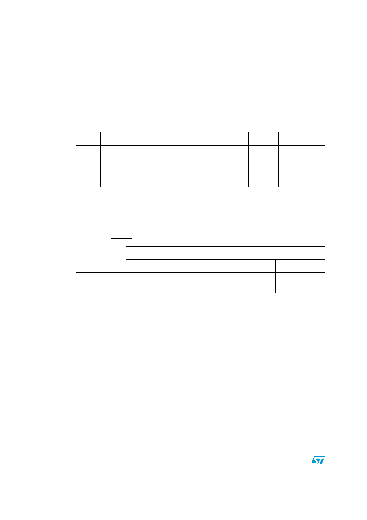
Table 3. V
Symbol Description Device Conditions Min Max
Rise time
DD
ST72324
Vt
PORVDD
Rise time
ST72324B (8K and 16K) 20ms/V
ST72324B (32K) Infinite ms/V
ST72F324, ST72F324B 100ms/V
2.2 Asynchronous RESET pin
The VIL/VIH of RESET pin has been changed from 0.16VDD/0.85VDD to 0.3VDD/0.7VDD
respectively (see Ta b le 4 ).
Table 4. RESET pin characteristics
ST72F324, ST72324 ST72F324B, ST72324B
Min Max Min Max
V
IL
V
IH
-0.16xVDD-0.3xV
0.85 x V
DD
2.3 Oscillator pad
The ST72324B (32K Flash and ROM devices only) features a new oscillator pad which is
more tolerant of the crystal type and is not disturbed if the oscillator pins are left
unconnected. When migrating to these devices, the MCU needs to be validated with your
existing resonator / crystal.
Infinite ms/V
LVD on 6µs/V
DD
-0.7xVDD-
4/8 Doc ID 12345 Rev 2

AN2366 Performance improvements
3 Performance improvements
The ST72F324B devices feature many significant improvements such as:
● Reduced PLL clock jitter
● Lower power consumption
● Improved A/D converter accuracy and negative injection on robust pins
Refer to the relevant datasheets for more details.
Doc ID 12345 Rev 2 5/8

Limitations summary AN2366
4 Limitations summary
Table 5. Limitation comparison table
Limitations ST72F324
(1)
ST72324
ROM
ST72F324B
ST72324B
ROM
Unexpected reset fetch XXXX
I/O Port A & F configuration
✔
(2)
X
✔ X
(2)
16-bit timer PWM mode XXXX
SCI Wrong break duration XXXX
Clearing active interrupts outside interrupt
routine
XXXX
External interrupt missed XXXX
TIMD set simultaneously with OC interruptXXXX
Internal RC operation X
Active Halt wake-up by external interrupt X
Negative injection current immunity on
analogic pins
V
(min) / VIL(max) 0.7 x VDD / 0.3 x VDD
IH
on reset pin
LVD/AVD operation ✔ X
Active Halt mode power consumption X
External clock source with PLL ✔ X
ICC mode entry with 39 pulses ✔✔X
Safe connection of OSC1/OSC2 pins X X ✔
Negative current injection on pin PB0 X ✔✔
1. Please refer to known limitations section in the datasheet.
2. For 8K/16K devices only.
3. Internal RC oscillator operation is not supported if LVD is disabled.
4. Only Reset or MCC/RTC interrupt can be used to exit from the Active Halt mode.
5. Negative injection current on any of the analog input pins significantly reduces the accuracy of ADC.
6. VIH(min) and VIL(max) on reset pin is 0.85 x V
7. LVD is not guaranteed.
8. For 8K/16K devices, if Readout Protection is selected, LVD may cause the product to become stuck in the
reset state.
9. Max power consumption in Active Halt mode is not guaranteed.
10. For 32K ROM devices, the power consumption in Active Halt mode is 190µA typical and 300µA maximum.
11. External clock source is not supported with PLL enabled.
12. Not supported for 8K/16K devices.
13. For 32K devices only.
14. Negative current injection is allowed only for 32K devices. For 8K/16K devices, limitation is still present.
(3)
(4)
(5)
X
(6)
X
(9)
and 0.16 x VDD respectively.
DD
X ✔✔
(4)
X
(5)
X
(6)
X
(7)
(9)
X
(11)
✔✔
✔✔
✔✔
✔✔
✔✔
(8)
(10)
✔✔
(12)
(13)
(14)
✔
(13)
✔
✔
Legend:
X - Limitation occurs.
✔ - No limitation.
6/8 Doc ID 12345 Rev 2

AN2366 Revision history
5 Revision history
Table 6. Document revision history
Date Revision Changes
07-Aug-2006 1 Initial release
01-Jul-2009 2
Updated Table 2: Feature overview and Table 5: Limitation
comparison table.
Doc ID 12345 Rev 2 7/8

AN2366
Please Read Carefully:
Information in this document is provided solely in connection with ST products. STMicroelectronics NV and its subsidiaries (“ST”) reserve the
right to make changes, corrections, modifications or improvements, to this document, and the products and services described herein at any
time, without notice.
All ST products are sold pursuant to ST’s terms and conditions of sale.
Purchasers are solely responsible for the choice, selection and use of the ST products and services described herein, and ST assumes no
liability whatsoever relating to the choice, selection or use of the ST products and services described herein.
No license, express or implied, by estoppel or otherwise, to any intellectual property rights is granted under this document. If any part of this
document refers to any third party products or services it shall not be deemed a license grant by ST for the use of such third party products
or services, or any intellectual property contained therein or considered as a warranty covering the use in any manner whatsoever of such
third party products or services or any intellectual property contained therein.
UNLESS OTHERWISE SET FORTH IN ST’S TERMS AND CONDITIONS OF SALE ST DISCLAIMS ANY EXPRESS OR IMPLIED
WARRANTY WITH RESPECT TO THE USE AND/OR SALE OF ST PRODUCTS INCLUDING WITHOUT LIMITATION IMPLIED
WARRANTIES OF MERCHANTABILITY, FITNESS FOR A PARTICULAR PURPOSE (AND THEIR EQUIVALENTS UNDER THE LAWS
OF ANY JURISDICTION), OR INFRINGEMENT OF ANY PATENT, COPYRIGHT OR OTHER INTELLECTUAL PROPERTY RIGHT.
UNLESS EXPRESSLY APPROVED IN WRITING BY AN AUTHORIZED ST REPRESENTATIVE, ST PRODUCTS ARE NOT
RECOMMENDED, AUTHORIZED OR WARRANTED FOR USE IN MILITARY, AIR CRAFT, SPACE, LIFE SAVING, OR LIFE SUSTAINING
APPLICATIONS, NOR IN PRODUCTS OR SYSTEMS WHERE FAILURE OR MALFUNCTION MAY RESULT IN PERSONAL INJURY,
DEATH, OR SEVERE PROPERTY OR ENVIRONMENTAL DAMAGE. ST PRODUCTS WHICH ARE NOT SPECIFIED AS "AUTOMOTIVE
GRADE" MAY ONLY BE USED IN AUTOMOTIVE APPLICATIONS AT USER’S OWN RISK.
Resale of ST products with provisions different from the statements and/or technical features set forth in this document shall immediately void
any warranty granted by ST for the ST product or service described herein and shall not create or extend in any manner whatsoever, any
liability of ST.
ST and the ST logo are trademarks or registered trademarks of ST in various countries.
Information in this document supersedes and replaces all information previously supplied.
The ST logo is a registered trademark of STMicroelectronics. All other names are the property of their respective owners.
© 2009 STMicroelectronics - All rights reserved
STMicroelectronics group of companies
Australia - Belgium - Brazil - Canada - China - Czech Republic - Finland - France - Germany - Hong Kong - India - Israel - Italy - Japan -
Malaysia - Malta - Morocco - Philippines - Singapore - Spain - Sweden - Switzerland - United Kingdom - United States of America
www.st.com
8/8 Doc ID 12345 Rev 2
 Loading...