

Page 1
AN2359
Application note
Double output Buck-Boost converter with VIPerX2A
Introduction
This paper introduces two off-line non-insulated SMPS double outputs in Buck–Boost
configuration based on VIPerX2A family The power supplies are operated in wide input
voltage range, i.e. 88 to 265VAC. They can supply small loads, such as a microcontroller,
triacs, display and peripherals in the industrial segment and home appliance. In the
applications where a double output is required, two different solutions can be used. The first
one regards an insulated converter topology, with second output generated by means of
one winding on the magnetic core of the inductor with a proper turns ratio. Nevertheless,
this solution is expensive in terms of transformer and can be used for medium and high
current or insulated applications. For low power and low cost applications, a non-insulated
converter topology can be used. The proposed topology, based on Buck-Boost converter, is
used to supply negative output voltage referred to neutral in all those applications where the
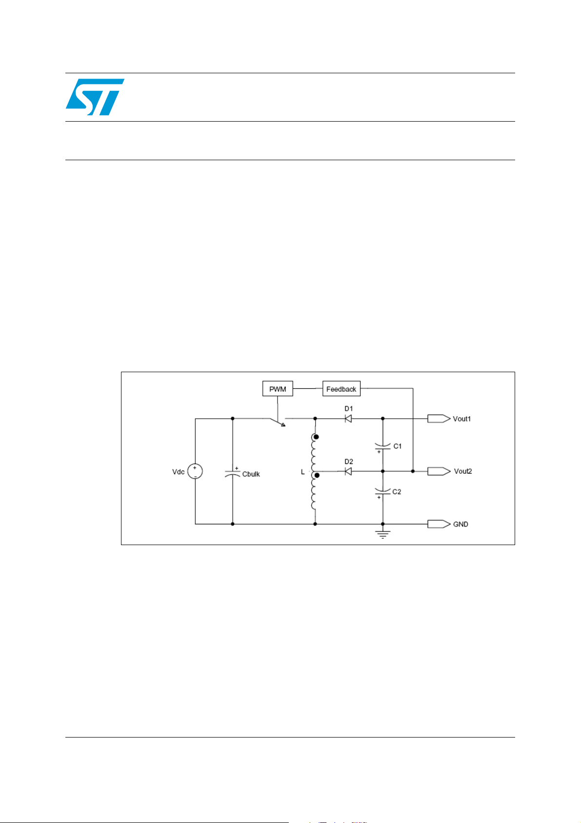
galvanic insulation is not required. The principle schematic is shown in figure below.
Proposed double output Buck-Boost topology
V
is provided using the classic Buck-Boost configurations, while V
OUT1
thanks to an intermediate tap on the inductor.
Compared to other already proposed solutions, the second output is obtained thanks to an
intermediate tap on a low cost inductor. This configuration limits the parasitic capacitive
effect between the two winding and improves the regulation at open load.
Further advantage is related to the regulation feedback connected on V
regulation, it is possible to cover those applications where a low tolerance and low voltage is
required (i.e. a microcontroller) and a high tolerance and high voltage is required for the
auxiliary circuit (drivers, relays…).
December 2006 Rev 1 1/18
is obtained
OUT2
. Thanks to this
OUT2
www.st.com
Page 2

Contents AN2359
Contents
1 VIPerX2 description . . . . . . . . . . . . . . . . . . . . . . . . . . . . . . . . . . . . . . . . . 5
2 Output voltage selection . . . . . . . . . . . . . . . . . . . . . . . . . . . . . . . . . . . . . 5
3 Application example nº 1 . . . . . . . . . . . . . . . . . . . . . . . . . . . . . . . . . . . . . 6
3.1 Experimental results . . . . . . . . . . . . . . . . . . . . . . . . . . . . . . . . . . . . . . . . . . 8
3.2 Thermal measurements . . . . . . . . . . . . . . . . . . . . . . . . . . . . . . . . . . . . . . 11
4 Application example nº 2 . . . . . . . . . . . . . . . . . . . . . . . . . . . . . . . . . . . . 12
4.1 Experimental results . . . . . . . . . . . . . . . . . . . . . . . . . . . . . . . . . . . . . . . . . 14
5 Layout considerations . . . . . . . . . . . . . . . . . . . . . . . . . . . . . . . . . . . . . . 15
6 Conclusions . . . . . . . . . . . . . . . . . . . . . . . . . . . . . . . . . . . . . . . . . . . . . . . 17
7 Revision history . . . . . . . . . . . . . . . . . . . . . . . . . . . . . . . . . . . . . . . . . . . 17
2/18
Page 3

AN2359 List of figures
List of figures
Figure 1. Converter schematic . . . . . . . . . . . . . . . . . . . . . . . . . . . . . . . . . . . . . . . . . . . . . . . . . . . . . . . 7
Figure 2. Typical waveforms at 88V
Figure 3. Typical waveforms at 88V
Figure 4. Typical waveforms at 265V
Figure 5. Typical waveforms at 265V
Figure 6. Commutation at full load: 88V
Figure 7. Commutation at full load: 265V
Figure 8. Output ripple voltage at full load: 88V
Figure 9. Output ripple voltage at full load: 265V
Figure 10. Turn on losses measurement at full load: 88V
Figure 11. Turn on losses measurement at full load: 265V
Figure 12. VIPer22A Thermal profile: at V
Figure 13. VIPer22A Thermal profile: at V
Figure 14. VIPer22A temperature at maximum load . . . . . . . . . . . . . . . . . . . . . . . . . . . . . . . . . . . . . . 12
Figure 15. Converter schematic. . . . . . . . . . . . . . . . . . . . . . . . . . . . . . . . . . . . . . . . . . . . . . . . . . . . . . 13
Figure 16. Typical waveforms at 300V
Figure 17. Typical waveforms at 300V
Figure 18. PCB Layout (not in scale). Option nº 1: -12V output voltage . . . . . . . . . . . . . . . . . . . . . . . 16
Figure 19. PCB Layout (not in scale). Option nº 2: -24V output voltage . . . . . . . . . . . . . . . . . . . . . . . 16
: open load . . . . . . . . . . . . . . . . . . . . . . . . . . . . . . . . . . . . . . . . 9
AC
: full load . . . . . . . . . . . . . . . . . . . . . . . . . . . . . . . . . . . . . . . . . 9
AC
: open load . . . . . . . . . . . . . . . . . . . . . . . . . . . . . . . . . . . . . . 10
AC
: full load . . . . . . . . . . . . . . . . . . . . . . . . . . . . . . . . . . . . . . . 10
AC
. . . . . . . . . . . . . . . . . . . . . . . . . . . . . . . . . . . . . . . . . . . . . 10
AC
. . . . . . . . . . . . . . . . . . . . . . . . . . . . . . . . . . . . . . . . . . . . 10
AC
= 88VAC. . . . . . . . . . . . . . . . . . . . . . . . . . . . . . . . . . . . . . 11
IN
= 265VAC. . . . . . . . . . . . . . . . . . . . . . . . . . . . . . . . . . . . . 11
IN
and full load: commutation . . . . . . . . . . . . . . . . . . . . . . . . . 15
DC
and full load: detail . . . . . . . . . . . . . . . . . . . . . . . . . . . . . . . 15
DC
. . . . . . . . . . . . . . . . . . . . . . . . . . . . . . . . . . . . . . . 10
AC
. . . . . . . . . . . . . . . . . . . . . . . . . . . . . . . . . . . . . . 10
AC
. . . . . . . . . . . . . . . . . . . . . . . . . . . . . . . . 11
AC
. . . . . . . . . . . . . . . . . . . . . . . . . . . . . . . 11
AC
3/18
Page 4

List of tables AN2359
List of tables
Table 1. Proposed converters. . . . . . . . . . . . . . . . . . . . . . . . . . . . . . . . . . . . . . . . . . . . . . . . . . . . . . . 5
Table 2. SMPS specifications . . . . . . . . . . . . . . . . . . . . . . . . . . . . . . . . . . . . . . . . . . . . . . . . . . . . . . . 6
Table 3. Component list . . . . . . . . . . . . . . . . . . . . . . . . . . . . . . . . . . . . . . . . . . . . . . . . . . . . . . . . . . . 7
Table 4. Circuit characterization - V
Table 5. Circuit characterization - V
Table 6. Circuit characterization - V
Table 7. SMPS specifications . . . . . . . . . . . . . . . . . . . . . . . . . . . . . . . . . . . . . . . . . . . . . . . . . . . . . . 12
Table 8. Component list . . . . . . . . . . . . . . . . . . . . . . . . . . . . . . . . . . . . . . . . . . . . . . . . . . . . . . . . . . 13
Table 9. Experimental results - V
Table 10. Experimental results - V
Table 11. Experimental results - V
Table 12. Revision history . . . . . . . . . . . . . . . . . . . . . . . . . . . . . . . . . . . . . . . . . . . . . . . . . . . . . . . . . 17
= 120VDC . . . . . . . . . . . . . . . . . . . . . . . . . . . . . . . . . . . . . . . . 8
IN
= 320VDC . . . . . . . . . . . . . . . . . . . . . . . . . . . . . . . . . . . . . . . . 8
IN
= 374VDC . . . . . . . . . . . . . . . . . . . . . . . . . . . . . . . . . . . . . . . . 9
IN
=120VDC . . . . . . . . . . . . . . . . . . . . . . . . . . . . . . . . . . . . . . . . . . 14
IN
=320VDC . . . . . . . . . . . . . . . . . . . . . . . . . . . . . . . . . . . . . . . . . . 14
IN
=374VDC . . . . . . . . . . . . . . . . . . . . . . . . . . . . . . . . . . . . . . . . . . 15
IN
4/18
Page 5

AN2359 VIPerX2 description
1 VIPerX2 description
The proposed converters are based on The VIPerX2A family, which is a range of smart
power devices with current mode PWM controller, start-up circuit and protections integrated
in a monolithic chip using VIPower M0 Technology.
The VIPerX2A family includes:
– VIPer12, with a 0.4A peak drain current limitation and 730V breakdown voltage;
– VIPer22, with a 0.7A peak drain current limitation and 730V breakdown voltage.
The switching frequency is internally fixed at 60kHz by the integrated oscillator of the
VIPerX2.
The internal control circuit offers the following benefits:
– Large input voltage range on the V DD pin accommodates changes in supply
voltage;
– Automatic burst mode in low load condition;
– Overload protection in hiccup mode.
The feedback pin FB is sensitive to current and controls the operation of the device.
2 Output voltage selection
Two converters with different output voltage are introduced in this paper. The main
specifications are listed in Table 1.
Table 1. Proposed converters
Output 1 Output 2 P
-12V/150mA -5V/300mA 3.3W
-24V/100mA -5V/300mA 3.9W
As already discussed, V
This imposes, for the two solutions, a different design of the output inductor in terms of turns
ratio, i.e. n=1.4 for the –12V solution, against n=3.8 for the –24V solution (even if it could be
necessary to tune the turn ratio for proper output voltage).
Some disadvantage are related to the –12V solution:
– The parasitic capacitance effect between the two windings is increased, compared
to the second one. This will bring about higher switching losses in turn-on (see
Figure 10. and Figure 11.) and, consequently, a worsening in terms of efficiency;
– A higher voltage diode is needed to supply the VIPer;
– The peak current is twice higher, giving less output power margin for a given I
Therefore, a –24V/-5V solution can be suitably used for all those applications where
efficiency and cost are important and, in general, in all the designs where a –24V output
voltage does not impact on the cost of the relays and drivers.
is obtained by means of an intermediate tap on the inductor.
OUT2
OUT(MAX)
DLIM
.
5/18
Page 6

Application example nº 1 AN2359
Instead, the -12V/-5V solution can be used all those times where it is not possible to change
the auxiliary supply voltage.
3 Application example nº 1
The first application example is a 3.3W double output Buck-Boost converter. The
specifications are listed in Table 2.
The schematic of the circuit is shown in Figure 1. and the component list is shown in Table 3.
Table 2. SMPS specifications
Specification Value
Input voltage range, V
Output voltage V
Output voltage V
Maximum output current I
Maximum output current I
Maximum output power 3.3W
IN
OUT1
OUT2
OUT1
OUT2
The input voltage can range from 88V
to 265VAC. The input section consists in a resistor
AC
88 - 265V
-12V
-5V
150mA
300mA
AC
as a fuse, a single input rectifier diode and an input C-L-C filter. Such a filter provides both
DC voltage stabilization and EMI filtering. The C
SN-RSN
leg across D1 helps the further
reducing of the conducted emissions.
The regulation feedback is connected to V
zener diode D
precision depends on D
, in order to provide an output voltage with tight regulation range (the output
Z2
tolerance). V
Z2
OUT1
by means of the PNP transistor Q1 and
OUT2
is obtained thanks to the turns ratio of the
transformer.
The output inductor is wound in a TDK drum ferrite core (SRW0913 type), with an
intermediate tap for V
● L
● N
● N
= 420µH;
1-3
= 70 turns;
1-2
= 62 turns.
2-3
Optional bleeder resistors, R
. The specifications are the following:
OUT2
and Rb2, can be connected to the outputs in order to improve
b1
the regulation.
In particular, R
is full loaded and V
6/18
has to be chosen in order to avoid the overvoltage on V
b1
is in no load condition.
OUT1
OUT1
when V
OUT2
Page 7

AN2359 Application example nº 1
Figure 1. Converter schematic
Table 3. Component list
Reference Value Description
R
R
R
SN
b1
C
D
D
FUSE
, R
R
2
R
3
, R
C
SN
, C
1
C
3
C
4
C
5
C
6
C
7
C
8
D
1
, D
2
, D
4
D
Z1
D
Z2
Q
1
L
1
1
b2
2
3
5
22Ω, 1/2W Metallic oxide resistor
1.2KΩ, 1/4W Resistor
22Ω, 1/2W Resistor
68Ω, 1/4W Resistor
Optional resistor
0.1µF, 400V Polyester capacitor
10µF, 400V Electrolytic capacitor
10µF, 50V Electrolytic capacitor
22nF, 35V Ceramic capacitor
0.47µF, 50V Electrolytic capacitor
4.7µF, 50V Electrolytic capacitor
220µF, 16V Electrolytic capacitor
470µF, 16V Electrolytic capacitor
Diode 1N4007
Diode BA157
Diode STTH106 (ultrafast)
Diode Zener 6.8V
Diode Zener 4.3V
PNP transistor BC558
470µH Axial inductor
7/18
Page 8
Application example nº 1 AN2359
Table 3. Component list (continued)
Reference Value Description
L
2
IC STMicroelectronics VIPer22ADIP
(Read sec. 5)
3.1 Experimental results
The power supply has been characterized in terms of line and load regulation. The
efficiency measurements have been taken using a DC power source and a
milliamperometer, in order to have higher accuracy than in AC measurements. In Tab le
4.,Table 5. and Table 6. the experimental results are shown. It is then possible to observe
the efficiency decreases, at same output power, when V
explained with an increase of the parasitic capacitance effect between the windings. These
measurements have been performed without bleeder resistors. Consequently, an
overvoltage occurs on V
can be avoided adding a 3.3KW resistor as a bleeder, with only a slight reduction of the
efficiency. In Figure 2., Figure 3., Figure 4., Figure 5., Figure 6., and Figure 7. typical
waveforms at minimum and maximum input voltage are shown. Figure 8. and Figure 9.
shows the output ripple voltage at full load at minimum and maximum input voltage. In
Figure 10. and Figure 11. turn-on losses measurements are shown in the same previous
conditions. It is important to point out that a lot of power is dissipated in turn-on, due to the
parasitic capacitance of the inductor.
Table 4. Circuit characterization - VIN = 120V
I
[mA] I
OUT1
OUT2
[mA] V
OUT1
OUT1
is more loaded. This can be
OUT2
when it is in no load condition and V
DC
[V] V
[V] IIN [mA] PIN [W] P
OUT2
is full loaded. This
OUT2
[W]
OUT
η [%]
0 0 12.00 5.01 1.08 0.129 0 0
0 150 14.73 4.99 9.71 1.16 0.784 67.58
0 300 16.04 4.97 18.33 2.20 1.49 67.70
75 0 10.51 5.00 8.86 1.06 0.788 74.30
75 150 11.15 4.97 17.60 2.11 1.58 74.80
75 300 11.32 4.95 27.10 3.25 2.33 71.70
150 0 10.40 4.99 16.81 2.02 1.56 77.20
150 150 10.95 4.95 26.40 3.17 2.38 75.00
150 300 11.14 4.92 36.60 4.40 3.15 71.50
Table 5. Circuit characterization - VIN = 320V
I
[mA] I
OUT1
0 0 11.77 5.04 0.47 0.15 0.00 0.00
0 150 15.56 5.02 3.89 1.24 0.75 60.49
0 300 16.26 5.01 7.25 2.32 1.50 64.78
75 0 10.55 5.02 3.55 1.14 0.79 69.65
OUT2
[mA] V
OUT1
[V] V
[V] IIN [mA] PIN [W] P
OUT2
DC
OUT
[W]
η [%]
8/18
Page 9

AN2359 Application example nº 1
Table 5. Circuit characterization - VIN = 320V
I
OUT1
[mA] I
OUT2
[mA] V
OUT1
[V] V
[V] IIN [mA] PIN [W] P
OUT2
DC
OUT
[W]
75 150 11.23 5.01 7.01 2.24 1.59 71.05
75 300 11.37 4.99 10.53 3.37 2.35 69.73
150 0 10.4 5.01 6.7 2.14 1.56 72.76
150 150 11.01 5 10.38 3.32 2.40 72.30
150 300 12.21 4.98 14.44 4.62 3.33 71.97
Table 6. Circuit characterization - VIN = 374V
I
OUT1
[mA] I
OUT2
[mA] V
OUT1
[V] V
[V] IIN [mA] PIN [W] P
OUT2
DC
OUT
[W]
0 0 11.74 5.06 0.44 0.16 0.00 0.00
0 150 15.77 5.02 3.39 1.27 0.75 59.39
0 300 16.51 5 6.38 2.39 1.50 62.86
75 0 10.54 5.02 3.09 1.16 0.79 68.40
75 150 11.26 5.01 6.18 2.31 1.60 69.05
75 300 11.41 5 9.36 3.50 2.36 67.29
150 0 10.4 5.01 5.92 2.21 1.56 70.46
η [%]
η [%]
150 150 11.05 5.01 9.26 3.46 2.41 69.56
150 300 11.2 4.98 12.74 4.76 3.17 66.61
Figure 2. Typical waveforms at 88VAC: open
load
Ch1 Freq - 2.38kHz
Ch2 Max - 228mA
Figure 3. Typical waveforms at 88VAC: full
load
Ch1 Freq - 59.61kHz
Ch2 Max - 572mA
9/18
Page 10

Application example nº 1 AN2359
Figure 4. Typical waveforms at 265VAC: open
Figure 6. Commutation at full load: 88V
load
Ch1 Freq - 2.39kHz
Ch2 Max - 428mA
Ch1 Freq - 103V
AC
A
m
2
6
5
-
x
a
M
2
h
C
Figure 5. Typical waveforms at 265VAC: full
load
Ch1 Freq - 59.65kHz
Ch2 Max - 532mA
Figure 7. Commutation at full load: 265V
V
x
a
-
h
M
C
A
m
0
3
5
-
x
a
M
2
h
C
1
6
3
6
AC
Figure 8. Output ripple voltage at full load:
88V
10/18
AC
Ch1 Pk-Pk - 90mV
Ch3 Pk-Pk - 80mV
Figure 9. Output ripple voltage at full load:
265V
AC
Ch1 Pk-Pk - 108mV
Ch3 Pk-Pk - 82mV
Page 11

AN2359 Application example nº 1
Figure 10. Turn on losses measurement at full
load: 88V
AC
M1 Area 2.92µWs
3.2 Thermal measurements
In this application, the main thermal issues are related to parasitic capacitance effects that
can lead to higher power dissipation in the device and then higher working temperature. In
order to evaluate the case temperature of the VIPer in the entire input voltage range, a
thermal mapping by means of an IR Camera was done at ambient temperature and full load.
In Figure 12. and Figure 13. the thermal profile of the device at minimum and maximum
input voltage range respectively is shown. It is important to highlight that at low line the
conduction losses are predominant, instead at high input voltage the switch losses became
not negligible, due to parasitic capacitance of the inductor. This is point out in Figure 14.
Figure 11. Turn on losses measurement at full
load: 265V
M1 Area 10.07µWs
AC
Figure 12. VIPer22A Thermal profile: at VIN=
88V
T
CASE(MAX)
AC
=53.3°C
Figure 13. VIPer22A Thermal profile: at VIN=
265V
AC
T
CASE(MAX)
=67.3°C
11/18
Page 12

Application example nº 2 AN2359
Figure 14. VIPer22A temperature at maximum load
4 Application example nº 2
In this second example, the Buck-Boost is modified in order to have –24V/-5Voutputs
voltages in a 4W application. In Table 7. the main specifications of the power supply are
listed. The schematic of the circuit and the component list are shown in Figure 15. and in
Table 8. respectively.
Table 7. SMPS specifications
Specification Value
Input voltage range, V
Output voltage V
Output voltage V
Maximum output current I
Maximum output current I
Maximum output power 4W
The –24V output voltage allows to supply the VIPer directly from the feedback path, saving
the cost of a high voltage diode. Even in this case, the feedback regulation is connected to
V
by means of Q1 transistor and DZ1 zener diode. The output inductor, with
OUT2
intermediate tap for V
, is provided by PULSE (PFM0250 type) with the following
OUT2
features:
● L
● N
● R
● R
= 510µH ±10%;
1-3
/ N
1-3
1-2
2-3
= 3.81 ± 2%;
2-3
= 560mW (max);
260ΩW (max).
IN
OUT1
OUT2
OUT1
OUT2
88 - 265V
-24V
-5V
100mA
300mA
AC
12/18
Page 13

AN2359 Application example nº 2
Also bleeder resistors or zener diodes may be mandatory at no load in order to improve the
regulation and avoid output overvoltage.
Figure 15. Converter schematic
Table 8. Component list
Reference Value Description
R
R
R
C
D
2
FUSE
, R
SN
R
2
R
3
, R
b1
b2
C
SN
, C
1
2
C
3
C
4
C
6
C
7
C
8
D
1
, D4, D
D
Z1
D
Z2
Q
1
L
1
1
5
22Ω, 1/2W Metallic oxide resistor
1.2KΩ, 1/4W Resistor
22Ω, 1/4W Resistor
100Ω, 1/4W Resistor
0.1µF, 400V Polyester capacitor
10µF, 400V Electrolytic capacitor
33µF, 25V Electrolytic capacitor
47nF, 35V Ceramic capacitor
22µF, 16V Electrolytic capacitor
470µF, 25V Electrolytic capacitor
100µF, 16V Electrolytic capacitor
Diode BYT11-400 (ultrafast)
PNP transistor BC327
470µH Axial inductor
Optional resistor
Diode 1N4007
Diode Zener 18V
Diode Zener 4.3V
13/18
Page 14

Application example nº 2 AN2359
Table 8. Component list (continued)
Reference Value Description
L
2
(Read sec. 6) Pulse PFM0250
IC STMicroelectronics
4.1 Experimental results
In Table 9., Tab l e 10 . and Ta b l e 11 . the measures performed on the proposed converter are
listed. In Figure 16. and Figure 17. typical waveforms at 300V
The converter performs well in terms of line and load regulation. The –5V output shows a
±5% of precision. V
performance too, even if an overvoltage occurs on V
V
is full loaded. This can be avoided connecting an appropriate bleeder resistor on
OUT2
V
. The efficiency measurements show a better behavior compared to the –12V
OUT1
solution. This can be explained because, in this configuration, the turn-on losses are lower
compared to the –12V solution.
Table 9. Experimental results - VIN=120V
I
[mA] I
OUT1
0 0 24.09 5.096 0.986 0.1972 0 0.00
10 30 23.87 5.098 3.643 0.7286 0.39164 53.75
50 150 23.97 5.087 13.33 2.666 1.96155 73.58
80 240 24.05 5.075 20.5 4.1 3.142 76.63
100 300 24.06 5.069 25.68 5.136 3.9267 76.45
OUT2
[mA] V
, obtained by means of the turns ratio of the inductor, shows good
OUT1
OUT1
[V] V
when it is in no load condition and
OUT1
DC
[V] IIN[mA] PIN[W] P
OUT2
are shown.
DC
[W] η[%]
OUT
0 300 41.54 5.02 12.74 2.55 1.51 59.11
100 0 21.82 5.083 13.74 2.75 2.18 79.40
Table 10. Experimental results - VIN=320V
I
[mA] I
OUT1
0 0 24.1 5.098 0.666 0.20 0.00 0.00
10 30 23.9 5.094 2.435 0.73 0.39 53.64
50 150 23.96 5.091 9.182 2.75 1.96 71.21
80 240 24.03 5.079 13.85 4.16 3.14 75.60
100 300 24.03 5.068 17.17 5.15 3.92 76.17
0 300 41.14 5.025 8.684 2.61 1.51 57.87
100 0 21.89 5.096 9.41 2.82 2.19 77.54
14/18
OUT2
[mA] V
OUT1
[V] V
OUT2
DC
[V] IIN[mA] PIN[W] P
[W] η[%]
OUT
Page 15

AN2359 Layout considerations
Table 11. Experimental results - V
I
[mA] I
OUT1
0 0 24.16 5.098 0.513 0.21 0.00 0.00
10 30 23.99 5.094 1.852 0.74 0.39 53.01
50 150 24 5.094 7.04 2.82 1.96 69.75
80 240 24.03 5.085 10.66 4.26 3.14 73.71
100 300 24.028 5.071 13.14 5.26 3.92 74.66
0 300 41 5.03 6.68 2.67 1.51 56.47
100 0 21.93 5.1 7.221 2.89 2.19 75.92
OUT2
[mA] V
OUT1
[V] V
IN
OUT2
Figure 16. Typical waveforms at 300VDC and
full load: commutation
=374V
DC
[V] IIN[mA] PIN[W] P
[W] η[%]
OUT
Figure 17. Typical waveforms at 300VDC and
full load: detail
5 Layout considerations
A proper PCB layout is essential for correct operation of any switch-mode converter and the
same basic rules have to be taken into account in order to optimize the current path,
especially in high current path routing.
Since EMI issues are related to layout, the current loop area has to be minimized. Moreover,
the control ground path has to be separated from power ground, in order to avoid any noise
interference between the control section and the power section.
All the traces carrying high currents have to be as short as possible, in order to minimize the
resistive and inductive effect.
A particular care has to be taken into account regarding the optimal routing of the input EMI
filter path and the correct placement of any single component (L
bulk capacitors, trace as short as possible…).
–R1 very close to input
1
15/18
Page 16

Layout considerations AN2359
Finally, dissipating copper area on the VIPer drain and diodes pins have to be provided, in
order to increase the power dissipation capability and, consequently, reduce the devices
temperature.
The circuit layout is shown in figure 12 for the –12V configuration and in figure 13 for the –
24V configuration. The PCB is the same and includes the options for the two configurations.
Figure 18. PCB Layout (not in scale). Option nº 1: -12V output voltage
Figure 19. PCB Layout (not in scale). Option nº 2: -24V output voltage
16/18
Page 17

AN2359 Conclusions
6 Conclusions
Two low cost double outputs Buck-Boost converters have been proposed based on
STMicroelectronics VIPer22A.
Thanks to the regulation feedback connected to –5V output, the converters can be suitably
used to supply a microcontroller or applications where a high output voltage tolerance is
required.
Instead, the -12V or-24V output voltage, achieved by the output inductor turns ratio, can be
used for the auxiliary circuits where a lower tolerance can be accepted.
In particular, the –24V option can be preferred because it guarantees a higher efficiency
(due to lower turn- on losses) and allows to save the cost of a high voltage diode compared
to the –12V solution.
On the other side, the –12V solution has to be used in many applications when it is not
possible to change the auxiliary supply voltage from –12V to –24V.
The same topology can be used for lower power range, replacing the VIPer22 with the
VIPer12.
In this case the device can deliver up to about 2.2W.
7 Revision history
Table 12. Revision history
Date Revision Changes
04-Dec-2006 1 Initial release
17/18
Page 18

AN2359
Please Read Carefully:
Information in this document is provided solely in connection with ST products. STMicroelectronics NV and its subsidiaries (“ST”) reserve the
right to make changes, corrections, modifications or improvements, to this document, and the products and services described herein at any
time, without notice.
All ST products are sold pursuant to ST’s terms and conditions of sale.
Purchasers are solely responsible for the choice, selection and use of the ST products and services described herein, and ST assumes no
liability whatsoever relating to the choice, selection or use of the ST products and services described herein.
No license, express or implied, by estoppel or otherwise, to any intellectual property rights is granted under this document. If any part of this
document refers to any third party products or services it shall not be deemed a license grant by ST for the use of such third party products
or services, or any intellectual property contained therein or considered as a warranty covering the use in any manner whatsoever of such
third party products or services or any intellectual property contained therein.
UNLESS OTHERWISE SET FORTH IN ST’S TERMS AND CONDITIONS OF SALE ST DISCLAIMS ANY EXPRESS OR IMPLIED
WARRANTY WITH RESPECT TO THE USE AND/OR SALE OF ST PRODUCTS INCLUDING WITHOUT LIMITATION IMPLIED
WARRANTIES OF MERCHANTABILITY, FITNESS FOR A PARTICULAR PURPOSE (AND THEIR EQUIVALENTS UNDER THE LAWS
OF ANY JURISDICTION), OR INFRINGEMENT OF ANY PATENT, COPYRIGHT OR OTHER INTELLECTUAL PROPERTY RIGHT.
UNLESS EXPRESSLY APPROVED IN WRITING BY AN AUTHORIZED ST REPRESENTATIVE, ST PRODUCTS ARE NOT
RECOMMENDED, AUTHORIZED OR WARRANTED FOR USE IN MILITARY, AIR CRAFT, SPACE, LIFE SAVING, OR LIFE SUSTAINING
APPLICATIONS, NOR IN PRODUCTS OR SYSTEMS WHERE FAILURE OR MALFUNCTION MAY RESULT IN PERSONAL INJURY,
DEATH, OR SEVERE PROPERTY OR ENVIRONMENTAL DAMAGE. ST PRODUCTS WHICH ARE NOT SPECIFIED AS "AUTOMOTIVE
GRADE" MAY ONLY BE USED IN AUTOMOTIVE APPLICATIONS AT USER’S OWN RISK.
Resale of ST products with provisions different from the statements and/or technical features set forth in this document shall immediately void
any warranty granted by ST for the ST product or service described herein and shall not create or extend in any manner whatsoever, any
liability of ST.
ST and the ST logo are trademarks or registered trademarks of ST in various countries.
Information in this document supersedes and replaces all information previously supplied.
The ST logo is a registered trademark of STMicroelectronics. All other names are the property of their respective owners.
© 2006 STMicroelectronics - All rights reserved
STMicroelectronics group of companies
Australia - Belgium - Brazil - Canada - China - Czech Republic - Finland - France - Germany - Hong Kong - India - Israel - Italy - Japan -
Malaysia - Malta - Morocco - Singapore - Spain - Sweden - Switzerland - United Kingdom - United States of America
www.st.com
18/18
 Loading...