

Page 1

AN2353
Application note
Designing an application with the ST10F27x devices
Introduction
This note gives advice on designing applications based on devices of the ST10F27x family
which includes the ST10F276, ST10F275, ST10F273, ST10F272 and ST10F271.
Six topics are covered:
■ Information and recommendations on using an external resonator with the on-chip
oscillator
■ Details on start-up configuration and necessary precautions
■ Filtering, decoupling and use of special pins
■ Recommendations to reduce ADC conversion errors
■ Memory interface
■ Interfacing with the L4969 CAN interface
April 2006 Rev 1 1/18
www.st.com
Page 2

Contents AN2353
Contents
1 Oscillator . . . . . . . . . . . . . . . . . . . . . . . . . . . . . . . . . . . . . . . . . . . . . . . . . . 4
1.1 Oscillator characteristics . . . . . . . . . . . . . . . . . . . . . . . . . . . . . . . . . . . . . . 4
1.2 Start-up time . . . . . . . . . . . . . . . . . . . . . . . . . . . . . . . . . . . . . . . . . . . . . . . . 5
1.3 PCB la yout for SST10F27x oscillator . . . . . . . . . . . . . . . . . . . . . . . . . . . . . 6
1.4 Oscillator and EMC . . . . . . . . . . . . . . . . . . . . . . . . . . . . . . . . . . . . . . . . . . 6
1.5 32 kHz oscillator . . . . . . . . . . . . . . . . . . . . . . . . . . . . . . . . . . . . . . . . . . . . . 6
2 Port0 start-up configuration . . . . . . . . . . . . . . . . . . . . . . . . . . . . . . . . . . . 7
2.1 Port0 . . . . . . . . . . . . . . . . . . . . . . . . . . . . . . . . . . . . . . . . . . . . . . . . . . . . . . 7
2.2 Port0 start-up configuration . . . . . . . . . . . . . . . . . . . . . . . . . . . . . . . . . . . . 9
3 Filtering / decoupling . . . . . . . . . . . . . . . . . . . . . . . . . . . . . . . . . . . . . . . 10
3.1 Decoupling on V18 pins . . . . . . . . . . . . . . . . . . . . . . . . . . . . . . . . . . . . . . 10
3.2 Decoupling on +5V supply . . . . . . . . . . . . . . . . . . . . . . . . . . . . . . . . . . . . 10
3.3 Filtering / EMC . . . . . . . . . . . . . . . . . . . . . . . . . . . . . . . . . . . . . . . . . . . . . 11
3.4 Unused general purpose pins . . . . . . . . . . . . . . . . . . . . . . . . . . . . . . . . . 11
4 Special pins . . . . . . . . . . . . . . . . . . . . . . . . . . . . . . . . . . . . . . . . . . . . . . . 12
4.1 External access enable/stand-by voltage supply pin (EA/VSTBY) . . . . . . 12
4.2 RPD Pin . . . . . . . . . . . . . . . . . . . . . . . . . . . . . . . . . . . . . . . . . . . . . . . . . . 12
5 Reset . . . . . . . . . . . . . . . . . . . . . . . . . . . . . . . . . . . . . . . . . . . . . . . . . . . . . 12
6 Analog Digital Converter (ADC) . . . . . . . . . . . . . . . . . . . . . . . . . . . . . . . 13
6.1 Volt age drop in the source resistance . . . . . . . . . . . . . . . . . . . . . . . . . . . 13
6.2 Poor charging of the ADC internal resistance . . . . . . . . . . . . . . . . . . . . . 13
6.3 Errors due to high frequencies from input signal . . . . . . . . . . . . . . . . . . . 14
6.4 Reducing ADC errors . . . . . . . . . . . . . . . . . . . . . . . . . . . . . . . . . . . . . . . . 14
6.5 Varef po wer-up and power-down sequence . . . . . . . . . . . . . . . . . . . . . . . 14
7 External memory interface . . . . . . . . . . . . . . . . . . . . . . . . . . . . . . . . . . . 15
8 Connecting to L4969 . . . . . . . . . . . . . . . . . . . . . . . . . . . . . . . . . . . . . . . . 16
2/18
Page 3

AN2353 Contents
9 Revision history . . . . . . . . . . . . . . . . . . . . . . . . . . . . . . . . . . . . . . . . . . . 17
3/18
Page 4
Oscillator AN2353
1 Oscillator
The ST10F27x can run with an external clock connected to the XTAL1 input pin of the
oscillator inverter or with a clock signal generated by a resonator connected to the XTAL1 /
XTAL2 pins. According to the device, two kinds of oscillators have been implemented:
● ST10F276E, ST10F275E and ST10F273E: Wide-swing oscillator
● ST10F272E/B and ST10F271E/B: Low-power oscillator
Moreover, the ST10F27x provides a new feature when the Real Time Clock module is used
and a reference clock is needed in Power Down mode. In this case, two possible
configurations may be selected by the user application according to the desired level of
power reduction:
● A 32 kHz crystal is connected to the on-chip 32 kHz oscillator (pins XTAL3 / XTAL4)
and running. In this case, the main oscillator is stopped when Power Down mode is
entered, while the Real Time Clock continues counting using the 32 kHz clock signal as
reference.
● Only the main oscillator is running (XTAL1 / XTAL2 pins). In this case, the main
oscillator is not stopped when Power Down is entered and the Real Time Clock
continues counting using the main oscillator clock signal as reference.
Refer to the ST10F27x datasheet for the possible combinations. This chapter provides
detailed information on the use of the on-chip oscillator in conjunction with an external
resonator.
1.1 Oscillator characteristics
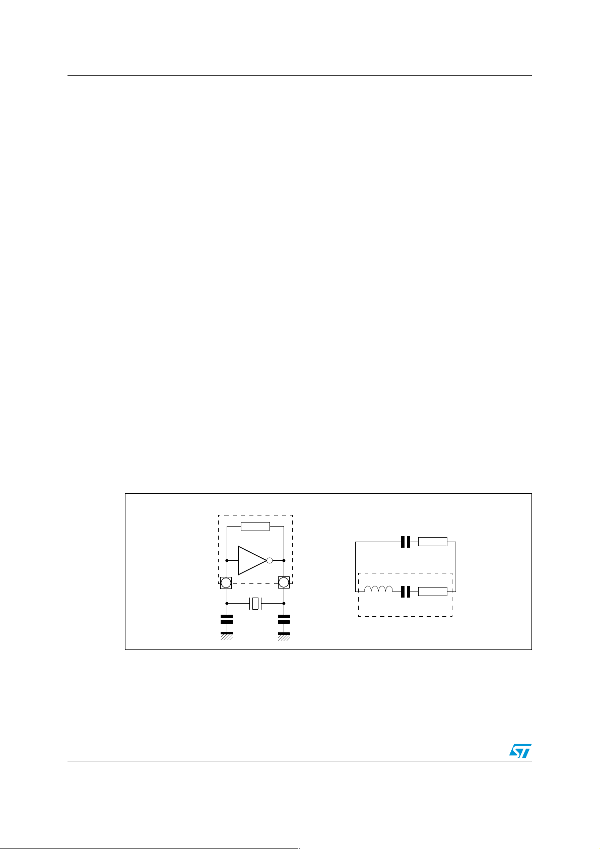
Although simple to implement, using an external resonator (crystal or ceramic resonator)
requires a few basic precautions. Referring to the schematic of the on-chip oscillator
(
Figure 1
Figure 1. Oscillator characteristics
The resonator component can be a crystal or a ceramic resonator. It is represented as a
series resonant branch R
replaced by a negative resistance R
capacitances and the stray capacitance of the resonator.
), the key items are described in the following section.
On-chip Oscillator circuit
g
m
XTAL1 XTAL2
C
Resonator
1
, Ls, Cs. The amplification ability of the oscillator inverter is
s
L
Equivalent circuit
C
L
R
L
C
L
C
2
s
Resonator
s
R
s
and the capacitance CL contains the C1 and C2 load
4/18
Page 5
AN2353 Oscillator
The load cap aci tor s C1 and C2 transf orm th e ga in o f t he am plif ier (gm) into a negative series
resistance R
The best frequency stability is obtained when C
of R
and Rs (the series resistance of the crystal) is negative.
L
By choosing C
to compensate for the losses of the crystal.
L
= C2. The oscillation occurs when the sum
1
= C2 = C, the minimal gain of the amplifier (gm) is expressed as follows:
1
gm
min
2
Rs C
×ω
× Rs C2× 2 π× f×()
2
×==
2
The minimal gain of the amplifier also implicitly sets the on-chip oscillator start-up time.
Table 1. g
Symbol Parameter Version Conditions
values for different types of oscillators
m
Value
Unit
Min Typ Max
g
m
Oscillator transconductance
The oscillation stability mainly depends on external parameters so only the
transconductance (g
measurement at the application level.
1.2 Start-up time
Ceramic resonators have a much shorter start-up time than crystals (about 100 times faster)
but have a lower accuracy on the frequency (initial tolerance, temperature variations and
drift).
Depending on applications
oscillator start-up time and frequency accuracy.
Fro m an S T 10 perspective, the w or s t ca se co nd i ti o n / environment for t h e o sc il l at or s tart-up
time is high temperature and low voltage.
Wide-swing 8 17 35
Low-power 0.7 2.5 6
32 kHz
) can be guaranteed and the start-up time value is defined by
m
Start-up 20 31 50
Norm al run 8 17 30
requirements and possibilities, users can choose between short
mA/V
µ A/V
5/18
Page 6
Oscillator AN2353
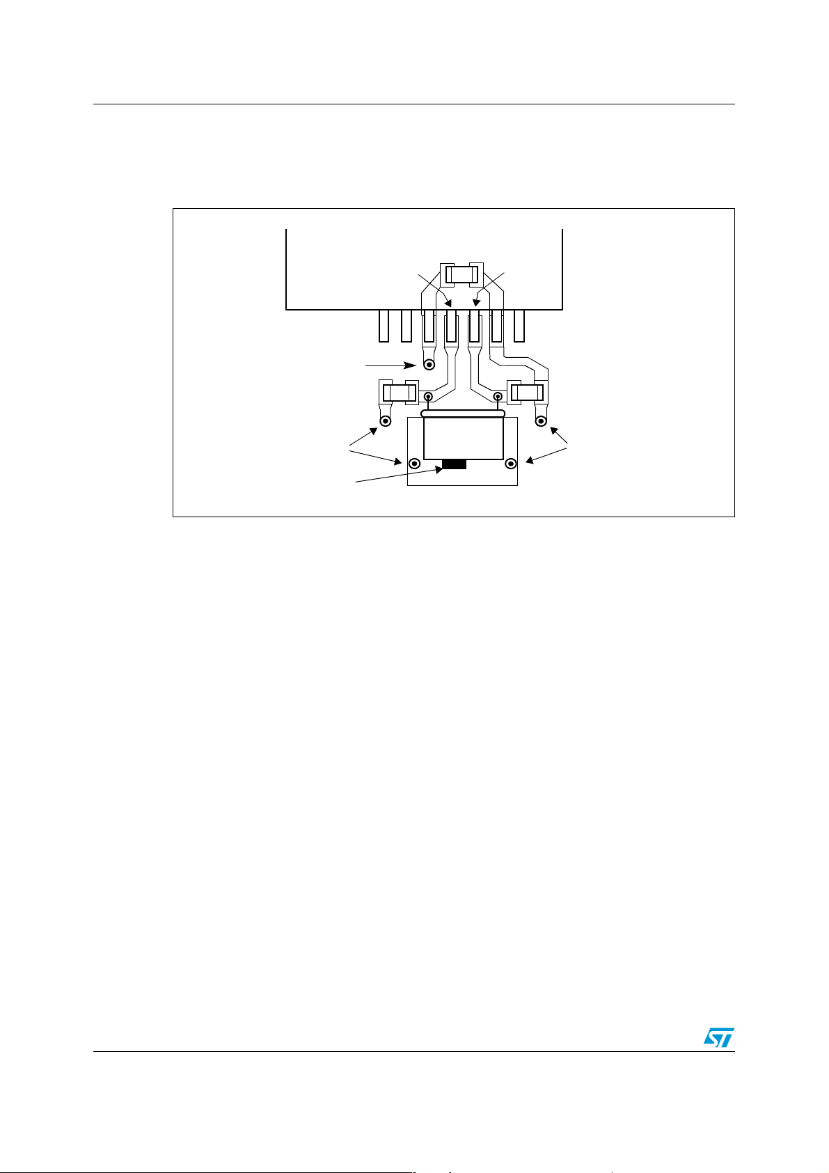
1.3 PCB layout for ST10F27x oscillator
The following
Figure 2
shows the proposed layout for the ST10F27x oscillator.
Figure 2. Example of layout for external crystal
ST10F27x
Vias to VDD
Vias to GND
Crystal package
soldered to GND
1.4 Oscillator and EMC
Decoupling capacitor
XT AL2
V
DD
C2
CD
Crystal
Ground plate
V
XTAL1
SS
C1
Vias to GND
The ST10F27x oscillator has an integrated gain control to minimize EMC and power
consumption. However, this does not prev ent users from observing / respecting the following
rules / recommendations:
● Avoid other high frequency signals near the oscillator circuitry . These can influence the
oscillator.
● Lay out/configure the ground supply on the basis of low impedance.
● Shield the crystal with an additional ground plane underneath the crystal.
● Do not lay out sensitive signals near the oscillator. Analyze cross-talk between different
layers.
● The V
pin close to the XTAL pins must be connected to the ground plane and
SS
decoupled to the closest V
● Capacitors are placed at both ends of the crystal, directly connected to the ground
plane while keeping the overall loop as small as possible.
● The crystal package, when metallic, is directly connected to the ground.
1.5 32 kHz oscillator
The same recommendations are valid for the 32 kHz oscillator. In any case, when the
32 kHz oscillator amplifier is not used, to avoid spurious consumption, XTAL3 must be tied
to ground while XTAL4 is left open. Moreover, bit OFF32 in the RTCCON register should be
set. The 32 kHz oscillator can only be driven by an external crystal and not by a different
clock source.
DD
pin.
6/18
Page 7

AN2353 Port0 start-up configuration
2 Port0 start-up configuration
A reset sequence may be triggered for the following reasons:
● Hardware reset signal on pin RSTIN (hardware reset input)
● Execution of the software reset instruction SRST
● Overflow of the Watchdog Timer
After recognition of a reset, the ST10F27x proceeds with the actions listed below:
● Complete internal RAM write operation before the internal reset procedure begins
● Cancel pending internal hold states
● Abort external memory access cycles
● Start program execution from memory location 0000h in code segment 0
Note: Please refer to the datasheet and user’s manual for reset event definitions.
2.1 Port0
Pull-down resistors
Pull-down resistors should be low enough so that the input voltage in P0.x is within the
circuit specification when taking into account the circuit pull-up current (see PORT0
configuration current for V
in=VILmax
) and other leakage currents from external circuits
connected to PORT0 pins.
R
< (V
pd
Recommended maximum value: R
)/ (I
ILmax
= 8KΩ; commonly used values, although larger than
pd
POl
+ I
other circuits
)
the calculated result, are 10KΩ.
Pull-up resistors
PORT0 supplies internal pul l-up resistors that are active during Reset. Pull-up resist ors
should be low enough so that the input voltage in P0.x is within the circuit specification when
taking into account the circuit pull-up current (see PORT0 configuration current for V
V
) and other leakage currents from external circuits connected to PORT0 pins. For
IHmin
worst case evaluation, leakage current from other external circuits should always be added
to circuit leakage current.
R
< (V
pu
No external pull-up resistor is necessary if I
Table 2
presents the clock options on PORT0 P0H.5 - P0H.7 for devices with low power
ddmin
- V
)/ (I
IHmin
other circuits
other circuits
< I
POH
- I
.
POh
)
oscillator.
Table 3
presents the clock options on PORT0 P0H.5 - P0H.7 for devices with wide-swing
oscillator.
=
in
7/18
Page 8

Port0 start-up configuration AN2353
Table 2. Clock options on PORT0 P0H.5/.7 for devices with low-power oscillator
P0H.7 P0H.6 P0H.5
111 f
110 f
101 f
100 f
011 f
010 f
001f
000 f
1. The external clock input range refers to a CPU clock range of 1...64 MHz.
2. The maximum input frequency depends on the duty cycle of the external clock signal (refer to the latest
datasheet).
3. The limit on input frequency is 4 to 8 MHz since the usage of the internal oscillator amplifier is required.
Also, when the PLL is not used and the CPU clock corresponds to FXTAL/2, an external crystal or
resonator should be used: It is not possible to force any clock with an external clock source.
Table 3. Clock options on PORT0 P0H.5 /.7 for devices with wide-swing oscillator
P0H.7 P0H.6 P0H.5
CPU frequency
f
CPU
= f
XTAL
XTAL
XTAL
XTAL
XTAL
XTAL
XTAL
XTAL
x F
XTAL
x 4 4 to 8 MHz Default configuration
x 3 5.3 to 8 MHz
x 8 4 to 8 MHz
x 5 6.4 to 8 MHz
x 1 1 to 64 MHz Direct drive
x 10 4 to 6.4 MHz
x 0.5 4 to 8 MHz CPU clock via prescaler
x 16 4 MHz
CPU frequency
f
CPU
= f
XTAL
x F
External clock
input range
External clock
input range
(1)
(1)
Notes
(2)
Notes
(3)
111 f
110 f
101 f
100 f
011 f
010 f
001f
000 f
1. The external clock input range refers to a CPU clock range of 1...64 MHz.
2. The maximum input frequency depends on the duty cycle of the external clock signal (refer to the latest
datasheet).
3. The limit on input frequency is 4 to 12 MHz since the usage of the internal oscillator amplifier is required.
Also when the PLL is not used and the CPU clock corresponds to FXTAL/2, an external crystal or resonator
shall be should be used: It is not possible to force any clock withan external clock source.
x 4 4 to 8 MHz Default configuration
XTAL
x 3 5.3 to 10.6 MHz
XTAL
x 8 4 to 8 MHz
XTAL
x 5 6.4 to 12 MHz
XTAL
x 1 1 to 64 MHz Direct drive
XTAL
x 10 4 to 6.4 MHz
XTAL
x 0.5 4 to 12 MHz CPU clock via prescaler
XTAL
x 16 4 MHz
XTAL
(2)
(3)
8/18
Page 9

AN2353 Port0 start-up configuration
2.2 Port0 start-up configuration
Figure 3
illustrates the usage of PORT0 pins to configure ST10F27x. All pins are sampled at
power-on reset but some of them are not sampled for specific reset conditions. For details,
please refer to the product datasheet and application note.
Figure 3. Port0 pin assignment for power-on configuration
V
DD
Internal
Pull-Up
Port0 during reset
P0L pin
External
Pull-Down
PORT0
P0H
P0L
P0H7
P0H6
P0H5
P0H4
P0H3
P0H2
P0H1
P0H0
P0L7
P0L6
P0L5
P0L4
P0L3
P0L2
P0L1
P0L0
Clock Options
(Refer to datasheet /
user’s manual
for PLL factor)
Segment Address Lines
Chip Selects
WR Configuration
Bustype (BTYP)
Startup Config ur ation
Bootstrap Loader Modes
Reserved
Reserved
Adapt Mode
Emulation Mode
9/18
Page 10

Filtering / decoupling AN2353
3 Filtering / decoupling
3.1 Decoupling on V18 pins
V18 is the output of the ST10F27x internal voltage regulator. It is available on the pac kage to
connect external decoupling capacitors.
A capacitor, X7R dielectric or equivalent, with a minimum value of 10nF (and maximum
100nF) must be connected between this pin and its nearest V
decouple the output of the internal regulator from the ground.
3.2 Decoupling on +5V supply
Decoupling capacitors are placed as close as possible to the chip VSS/VDD pins:
● Connected to both V
● Connected to each V
For EMC reasons, decoupling capacitors are connected to the V
pins. This is illustrated by
and VSS pins (adjacent pins)
DD
DD/VSS
Figure 4
pair
below:
pin. This is done to
SS
and VSS of adjacent
DD
Figure 4. Implementation of decoupling capacitors
Via to V
Via to V
ST10F27x
DD
Cap.
V
DD
Good implementation
Via to V
V
SS
SS
ST10F27x
Implementation to be avoided
SS
Cap.
V
Via to V
V
SS
DD
SS
10/18
Page 11

AN2353 Filtering / decoupling
3.3 Filtering / EMC
As ST10F27x has an internal voltage regulator, +5V pins are not differentiated between
output-buffers and internal logic. This means that when EMC filters are used to isolate the
CPU from the supply, all ST10F27x supply pins should be isolated with the filter(s).
Example of filter
Filter placed on supply line of the CPU to remove the conducted noise from the supply line
of the module (as illustrated in
Figure 5. Filter based on discrete components
Figure 5
).
ST10F269
+5V plane
C
GND plane
Filter connected to supply line of the CPU
3.4 Unused general purpose pins
Unused pins may be an additional source of noise if not properly connected.
Used pins must NOT be left floating.
Two configurations are possible:
1. Unused pins configured as input (default after reset)
Connect the unused pin to V
2. Unused pin configured as output (by user software)
The software sets the corresponding bit of the Direction Port Registers (DPPx) to
configure an unused pin as an output (set direction bit to 1) with level to V
0, default after reset). In this condition, the pad can be left unconnected on the board.
(directly or via a pull-down resistor)
SS
L
L
V
pins
DD
C
pins
V
SS
(data bit to
SS
Note: Avoiding floating pins in an application also ensures a good control on power consumption.
● Special handling for pins of Port 0 and Port 6
On the pins of Port 0 and Port 6, internal pull-ups are present (under Reset only). Our
recommendation is: to keep them open and configured by software as output (set direction
bit to 1) with output = 0 (data = 0).
● Special handling for pin P3.12 and BHE functionality
The pin P3.12 can be used as the B
interface. The BHE
alternate function is automatically enabled when the start-up
HE (Byte High Enable) signal for the external memory
configuration under Reset selects a 16-bit data bus.
11/18
Page 12

Special pins AN2353
There are two ways of disabling the BHE alternate function on P3.12:
– Select an 8-bit data bus size on Port0 during reset (pin P0L7 to V
– Disable it via bit BYTDIS of the SYSCON register.
SS
).
4 Special pins
4.1 External access enable/stand-by voltage supply pin
/V
(EA
A low level applied to this pin during and after reset forces the ST10F27x to start the
program execution from the external memory space. A high level will start the program
execution from internal memory.
STBY
)
If only internal memory is used, this pin can be tied directly to V
The EA
reset and main V
reference voltage for the low-power embedded voltage regulator which generates the
internal 1.8V supply for the XRTC module (when not disabled) and to retain data inside the
Stand-by portion of the XRAM (16 Kbyte). It can range from 4.5 to 5.5V.
/V
STBY
4.2 RPD Pin
The RPD pin (Return from Power-Down) generates the proper internal timing sequence
when interruptible power-down mode is used.
If the interruptible power-down mode is not used, the RPD pin can be connected to the
ground (directly or via a resistor of 1M maximum). In this configuration, the device always
performs asynchronous resets.
For more details, please refer to application note AN2340,
during Reset and Power-down mode.
5 Reset
.
DD
pin is also used (when Stand-by mode is entered, that is, ST10F27x under
turned off) to bias the 32 kHz oscillator amplifier circuit, to provide a
DD
ST10 RPD pin: Functionality
For information on ST10F27x reset, please refer to the product user manual.
12/18
Page 13

AN2353 Analog Digital Converter (ADC)
6 Analog Digital Converter (ADC)
Analog input signal error can be created by poor matching of the source internal resistance
with the ADC input parameters, which can be caused by the following occurences:
● Voltage drop in the voltage source resistance due to input leakage current
● Poor charging of the ADC internal capacitance (C
Analog input error can also be caused by noise from the analog input signal.
This section describes each of these causes.
Figure 6. Source internal resistance errors
R
SOURCE
V
S
P5.x
C
V
IN
IO
R1
I
OZ1
Leakage
Current
)
in
Sample
C
IN
AGND AGND
I
(Input leakage current Port5): maximum ± 200nA (test condition: 0.45V < VIN<VDD)
OZ1
CIO (Pin capacitance Port5): maximum 10pF (test condition: f = 1 MHz, TA= 25°C, guaranteed by design characterization)
C
(ADC internal capacitance): maximum 5pF (guaranteed by design characterization)
IN
R1 (Series input resistance): maximum 1.5kΩ (guaranteed by design characterization)
6.1 Voltage drop in the source resistance
The error generated by the voltage source internal resistance is:
R
---------------------------------------------V
I
= specified leakage current.
(OZ1)
error LS B()
Refer to the latest product datasheet for the value of I
×
SOURCEI0Z1()
–
AREFVAGND
(OZ1)
1024×=
.
Note: Input leakage current is caused by parasitic current into the on-chip protection of the
input pin; this protection is necessary to protect the device against ESD (Electrical Static
Discharge) and against overload.
6.2 Poor charging of the ADC internal resistance
During the sample time, the input capacitance (CIO and CIN) must be charged/discharged by
the external source. The internal resistance of the source must allow the capacitance to
reach its final value before the end of sample time.
If this does not happen, that is, if the source resistance is mismatched to the sample time, a
voltage loss occurs at the sample and hold stage. This voltage loss causes an accuracy loss
13/18
Page 14

Analog Digital Converter (ADC) AN2353
when increasing or decreasing the input voltage from Varef/2 (hold capacitor is precharged
to Varef/2 before sampling to reduce charge/discharge time).
Refer to the product data sheet for details.
6.3 Errors due to high frequencies from input signal
Small but high frequency signal variations can result in increased conversion error: During
sampling time, the analog signal is fed to an internal auto-zero circuitry. Signal variations (at
least two opposite transitions) during this time can generate auto-zero error. Signal
variations during sampling time generate excessively high or low conversion results; big
variations (Example: 150mV peak to peak variations at 1.5 MHz, with a 2.5V offset for 1µs
sampling time) can generates
Although the sample and hold internal circuitry is integrating signal variations, other internal
analog circuitry can be affected by signal transitions during sampling time.
The input analog signal should always be low pass filtered to ensure that high frequencies
are rejec ted.
clamped results (0x000 or 0x3FFh).
6.4 Reducing ADC errors
There are four possible optimizations:
● Minimize the total source impedance seen by the ST10
This means choosing sensors with low output impedance (not always easy for some
types of sensor) and minimizing the serial resistance of any protection devices between
the analog source and the input pin (while still providing a voltage protection level
compatible with the circuit specification).
● Match the sample time to the analog source impedance
● Match the sample time to the analog filter cut-off frequency to remove high frequencies
The ST10F27x sampling time (ADC silicon configuration) shall be should be / must be /
is 5 to 10 times shorter than the period of the cut-off frequency of the low-pass filter on
ADC input signal.
● Reduce noise at the input pin
Add an external RC filter (with attention to the source internal resistance). Compute the
average value of different samples in the software routine.
6.5 Varef power-up and power-down sequence
Varef should always be lower than the 5V supply (maximum = VDD+ 0.1V). This is
especially true for the power-up and power-down sequence when external devices are used
to generate Varef.
14/18
Page 15

AN2353 External memory interface
7 External memory interface
The ST10F27x external memory bus can easily interface with the STMicroelectronics
external Flash (M29Fxx series).
Please refer to application note AN1155
Flash Memories.
Connecting the ST10 Microcontroller to M29 Series
15/18
Page 16

Connecting to L4969 AN2353
8 Connecting to L4969
L4969 is a combined voltage regulator and low-speed CAN interface from
STMicroelectronics.
The following figure shows how to connect the L4969 CAN interface to the ST10F27x
microcontroller when working on an SPI bus with multiple peripherals.
Note: For further information on the L4969, please refer to the L4969 datasheet and the available
application notes for this device.
When no other peripherals are connected to the SPI bus, the L4969 can be directly
connected to the ST10 SPI lines without any further constraints.
Figure 7. ST10F27x connected to L4969 and other SPI devices
CS
L4969
CS
x
CS
y
SCLK
MTSR
MRST
RESET
Px.y
EN
NRES
NINT
CLK
EN
L4969
SOUT
Device x Device y
SIN
16/18
Page 17

AN2353 Revision history
9 Revision history
Table 4. Document revision history
Date Revision Changes
24-Apr-2006 1 Initial release
17/18
Page 18

AN2353
Please Read Carefully:
Information in this document is provided sole ly in connecti on with ST produ cts. STMicro electroni cs NV and its subsi diaries (“ST ”) reserve the
right to make changes , cor recti ons , modif ic ations or improv ement s, t o th is documen t, and the prod ucts an d servic es des crib ed he rein a t any
time, without notice.
All ST products are sold pursuant to ST’s terms and conditions of sale.
Purchasers are solely responsible for the c hoice, selection and use of the ST products and services described herein, and ST assumes no
liability whatsoever relating to the choice, selectio n or use of the ST products and services des cribed herein.
No license, express or implied, by estoppel or otherwise, to any intellectual property rights is granted under this document. If any part of this
document refers to any third party products or services it shall not be deemed a license grant by ST for the use of such third party products
or services, or any intellectual property contained therein or considered as a warranty covering the use in any manner whatsoever of such
third party products or services or any intellectual property contained therein.
UNLESS OTHERWISE SET FORTH IN ST’S TERMS AND CONDITIONS OF SALE ST DISCLAIMS ANY EXPRESS OR IMPLIED
WARRANTY WITH RESPECT TO THE USE AND/OR SALE OF ST PRODUCTS INCLUDING WITHOUT LIMITATION IMPLIED
WARRANTIES OF MERCHANTABILITY, FITNESS FOR A PARTICULAR PURPOSE (AND THEIR EQUIVALENTS UNDER THE LAWS
OF ANY JURISDICTION), OR INFRINGEMENT OF ANY PATENT, COPYRIGHT OR OTHER INTELLECTUAL PROPERTY RIGHT.
UNLESS EXPRESSLY APPROVED IN WRITING BY AN AUTHORIZE REPRESENTATIVE OF ST, ST PRODUCTS ARE NOT DESIGNED,
AUTHORIZED OR WARRANTED FOR USE IN MILITARY, AIR CRAFT, SPACE, LIFE SAVING, OR LIFE SUSTAINING APPLICATIONS,
NOR IN PRODUCTS OR SYSTEMS, WHERE FAILURE OR MALFUNCTION MAY RESULT IN PERSONAL INJURY, DEATH, OR
SEVERE PROPERTY OR ENVIRONMENTAL DAMAGE.
Resale of ST products with prov isions differen t from the state ments and/or tec hnical featur es set forth in th is document shall immediatel y void
any warranty granted by ST for the ST product or service described herein and shall not create or extend in any manner whatsoever, any
liability of ST.
ST and the ST logo are trademark s or registered trademark s of ST in various countries.
Information in this document su persedes and replaces all information previously supplied.
The ST logo is a registered trade mark of STMicroelectronics. All ot her names are the property of their respective owners.
© 2006 STMicroelectronics - All rights reserv ed
STMicroelectronics group of companies
Australia - Belgium - Brazil - Canada - China - Czech Republic - Finland - France - Germany - Hong Kong - India - Israel - Italy - Japan -
Malaysia - Malta - Morocco - Singapore - Spain - Sweden - Switzerland - United Kingdom - United States of America
www.st.com
18/18
 Loading...