

Page 1
AN2321
Application note
Reference design: high performance, L6599-based HB-LLC
adapter with PFC for laptop computers
Introduction
This note describes the performances of a 90 W, wide-range mains, power-factor-corrected
AC-DC adapter reference board. Its electrical specification is tailored on a typical hi-end
portable computer power adapter. The peculiarities of this design are the very low no-load
input consumption (<0.4 W) and the very high global efficiency.
The architecture is based on a two-st age approach: a front -end PFC pre-regulato r based on
the L6563 TM PFC controller and a downstream multi-resonant half-bridge converter that
makes use of the new L6599 resonant controller. The Standby function of the L6599,
pushing the DCDC converter upon recognition of a light load to work in burst mode and the
logic dedicated to stop the PFC stage allows meeting the severe no-load consumption
requirement.
The PFC TM operation and the top-level efficiency performance of the HB-LLC topology
provide also a very good overall efficiency of the circuit.
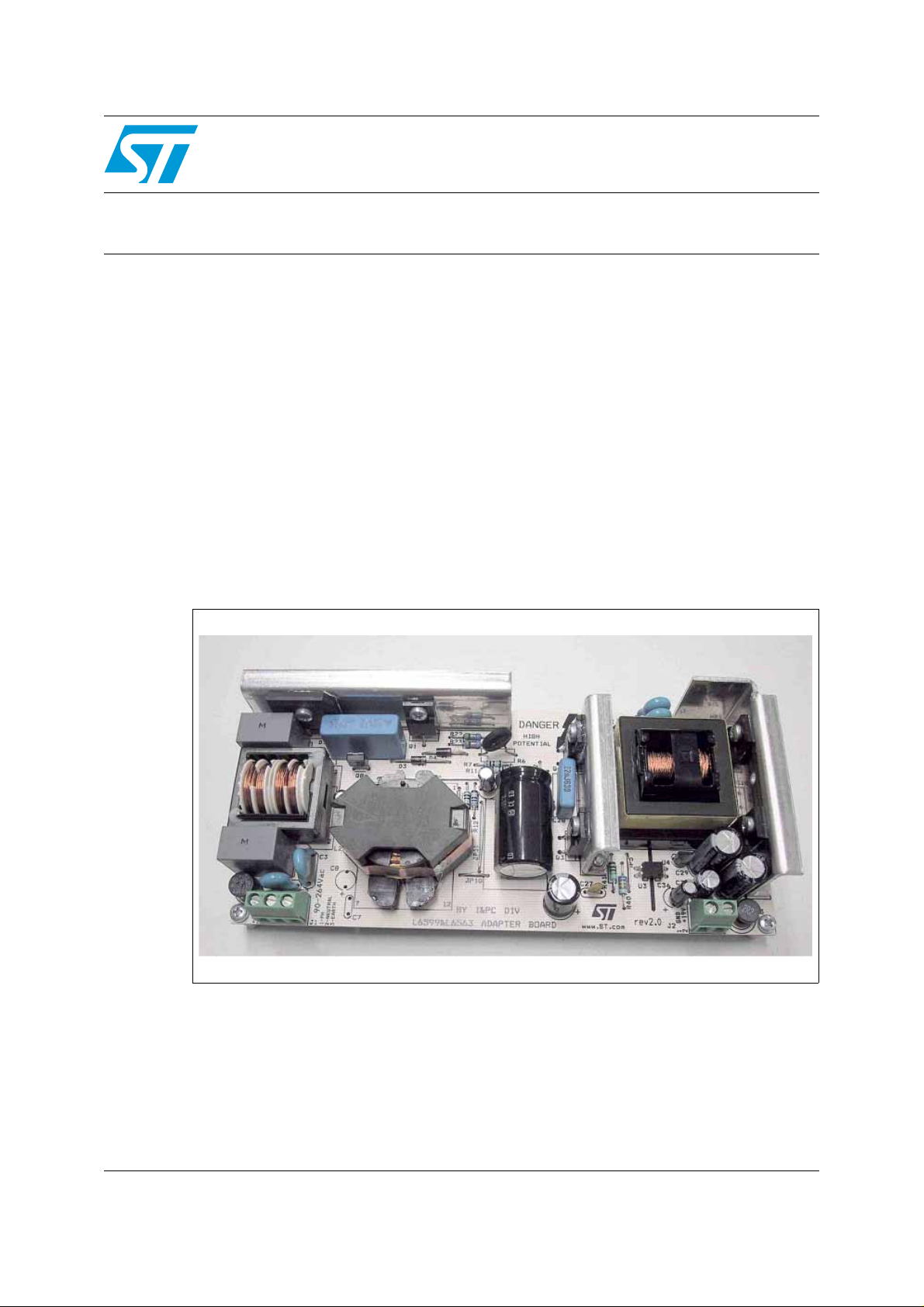
L6599 & L6563 90W - adapter demo-board (EVAL6599-90W)
May 2007 Rev 2 1/29
www.st.com
Page 2

Contents AN2321
Contents
1 Main characteristics and circuit description . . . . . . . . . . . . . . . . . . . . . 5
2 Test results . . . . . . . . . . . . . . . . . . . . . . . . . . . . . . . . . . . . . . . . . . . . . . . . 7
2.1 Efficiency measurements . . . . . . . . . . . . . . . . . . . . . . . . . . . . . . . . . . . . . . 7
2.2 Resonant stage operating waveforms . . . . . . . . . . . . . . . . . . . . . . . . . . . . 8
2.3 Stand-by & no load power consumption . . . . . . . . . . . . . . . . . . . . . . . . . . . 9
2.4 Short circuit protection . . . . . . . . . . . . . . . . . . . . . . . . . . . . . . . . . . . . . . . 12
2.5 Over voltage protections . . . . . . . . . . . . . . . . . . . . . . . . . . . . . . . . . . . . . 13
2.6 Start-up sequence . . . . . . . . . . . . . . . . . . . . . . . . . . . . . . . . . . . . . . . . . . 13
3 Thermal tests . . . . . . . . . . . . . . . . . . . . . . . . . . . . . . . . . . . . . . . . . . . . . . 15
4 Conducted emission pre-compliance test . . . . . . . . . . . . . . . . . . . . . . 17
5 Bill of material . . . . . . . . . . . . . . . . . . . . . . . . . . . . . . . . . . . . . . . . . . . . . 18
6 PFC coil specification . . . . . . . . . . . . . . . . . . . . . . . . . . . . . . . . . . . . . . . 23
6.1 Electrical characteristics . . . . . . . . . . . . . . . . . . . . . . . . . . . . . . . . . . . . . . 23
6.2 Mechanical aspect and pin numbering . . . . . . . . . . . . . . . . . . . . . . . . . . . 24
7 Resonant power transformer specification . . . . . . . . . . . . . . . . . . . . . 25
7.1 Electrical characteristics . . . . . . . . . . . . . . . . . . . . . . . . . . . . . . . . . . . . . . 25
7.2 Mechanical aspect and Pin numbering . . . . . . . . . . . . . . . . . . . . . . . . . . 26
8 PCB lay-out . . . . . . . . . . . . . . . . . . . . . . . . . . . . . . . . . . . . . . . . . . . . . . . 27
9 Revision history . . . . . . . . . . . . . . . . . . . . . . . . . . . . . . . . . . . . . . . . . . . 28
2/29
Page 3

AN2321 List of tables
List of tables
Table 1. Efficiency measurements - Vin=115 Vac . . . . . . . . . . . . . . . . . . . . . . . . . . . . . . . . . . . . . . . 7
Table 2. Efficiency measurements - Vin=230 Vac . . . . . . . . . . . . . . . . . . . . . . . . . . . . . . . . . . . . . . . 7
Table 3. Stand-by consumption - Vin=115 Vac . . . . . . . . . . . . . . . . . . . . . . . . . . . . . . . . . . . . . . . . 11
Table 4. Stand-by consumption - Vin=230 Vac . . . . . . . . . . . . . . . . . . . . . . . . . . . . . . . . . . . . . . . . 11
Table 5. Temperature of measured points @115 Vac - full load . . . . . . . . . . . . . . . . . . . . . . . . . . . 15
Table 6. Temperature of measured points @230 Vac - full load . . . . . . . . . . . . . . . . . . . . . . . . . . . 16
Table 7. Bill of material . . . . . . . . . . . . . . . . . . . . . . . . . . . . . . . . . . . . . . . . . . . . . . . . . . . . . . . . . . . 18
Table 8. Winding characteristics. . . . . . . . . . . . . . . . . . . . . . . . . . . . . . . . . . . . . . . . . . . . . . . . . . . . 23
Table 9. Winding characteristics. . . . . . . . . . . . . . . . . . . . . . . . . . . . . . . . . . . . . . . . . . . . . . . . . . . . 25
Table 10. Revision history . . . . . . . . . . . . . . . . . . . . . . . . . . . . . . . . . . . . . . . . . . . . . . . . . . . . . . . . . 28
3/29
Page 4

List of figures AN2321
List of figures
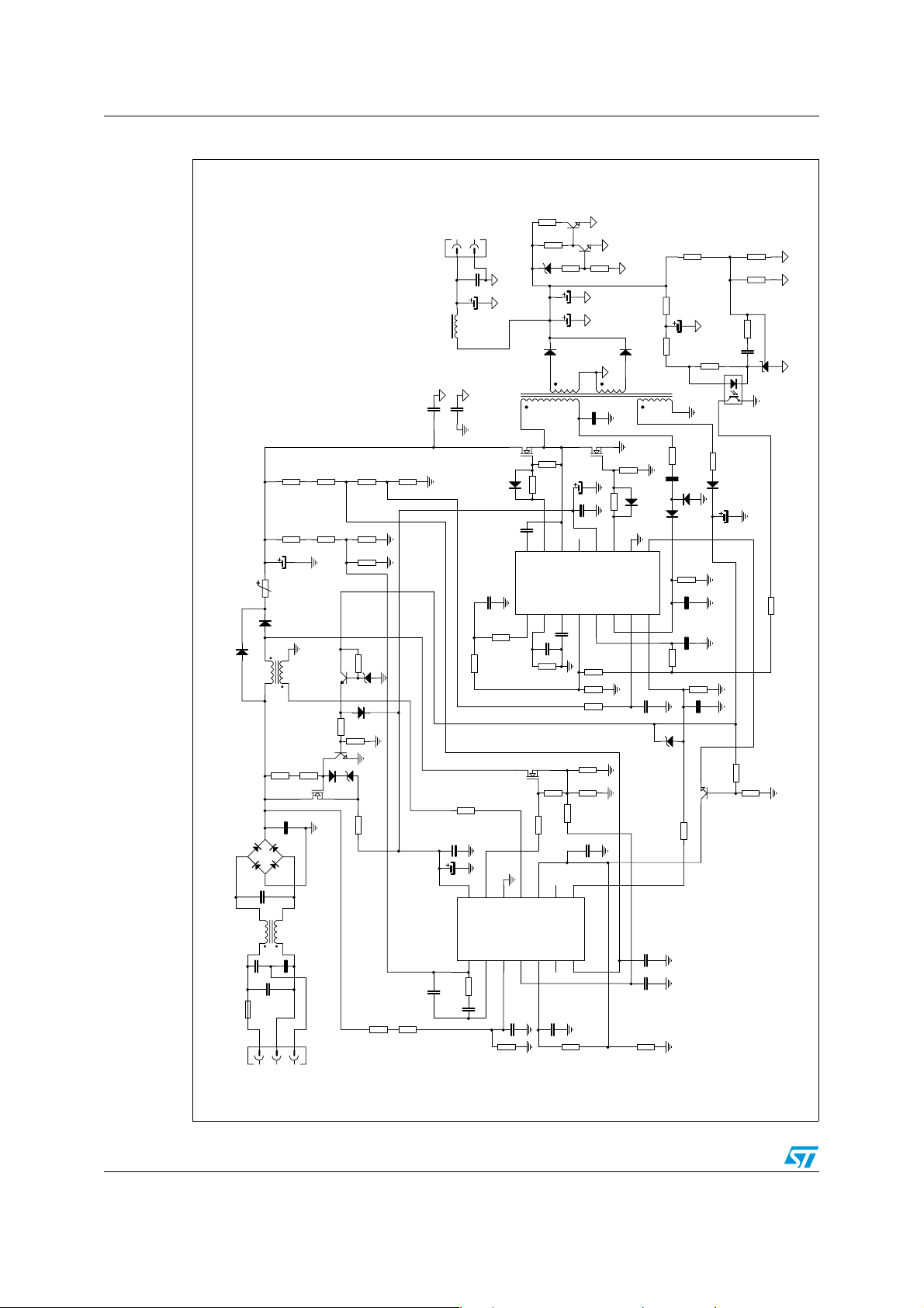
Figure 1. Electrical diagram . . . . . . . . . . . . . . . . . . . . . . . . . . . . . . . . . . . . . . . . . . . . . . . . . . . . . . . . 6
Figure 2. Efficiency vs. Pout . . . . . . . . . . . . . . . . . . . . . . . . . . . . . . . . . . . . . . . . . . . . . . . . . . . . . . . . 8
Figure 3. Resonant circuit primary side waveforms. . . . . . . . . . . . . . . . . . . . . . . . . . . . . . . . . . . . . . . 8
Figure 4. Resonant circuit secondary side waveforms . . . . . . . . . . . . . . . . . . . . . . . . . . . . . . . . . . . . 9
Figure 5. Input power without load vs. mains voltage . . . . . . . . . . . . . . . . . . . . . . . . . . . . . . . . . . . . 10
Figure 6. Waveforms at no-load operation. . . . . . . . . . . . . . . . . . . . . . . . . . . . . . . . . . . . . . . . . . . . . 10
Figure 7. Waveforms at no-load operation. . . . . . . . . . . . . . . . . . . . . . . . . . . . . . . . . . . . . . . . . . . . . 10
Figure 8. Load transition 0 ÷ 100% . . . . . . . . . . . . . . . . . . . . . . . . . . . . . . . . . . . . . . . . . . . . . . . . . . 11
Figure 9. Load transition 100% ÷ 0 . . . . . . . . . . . . . . . . . . . . . . . . . . . . . . . . . . . . . . . . . . . . . . . . . . 11
Figure 10. O/P short circuit waveforms . . . . . . . . . . . . . . . . . . . . . . . . . . . . . . . . . . . . . . . . . . . . . . . . 12
Figure 11. O/P short circuit waveforms (zoomed) . . . . . . . . . . . . . . . . . . . . . . . . . . . . . . . . . . . . . . . . 12
Figure 12. Start-up @115 Vac - full load . . . . . . . . . . . . . . . . . . . . . . . . . . . . . . . . . . . . . . . . . . . . . . . 13
Figure 13. Start-up @115 Vac - full load . . . . . . . . . . . . . . . . . . . . . . . . . . . . . . . . . . . . . . . . . . . . . . . 13
Figure 14. Thermal map @115 Vac - full load . . . . . . . . . . . . . . . . . . . . . . . . . . . . . . . . . . . . . . . . . . . 15
Figure 15. Thermal map @230 Vac - full load . . . . . . . . . . . . . . . . . . . . . . . . . . . . . . . . . . . . . . . . . . . 16
Figure 16. CE peak measure at 115 Vac and full load . . . . . . . . . . . . . . . . . . . . . . . . . . . . . . . . . . . . 17
Figure 17. CE peak measure at 230 Vac and full load . . . . . . . . . . . . . . . . . . . . . . . . . . . . . . . . . . . . 17
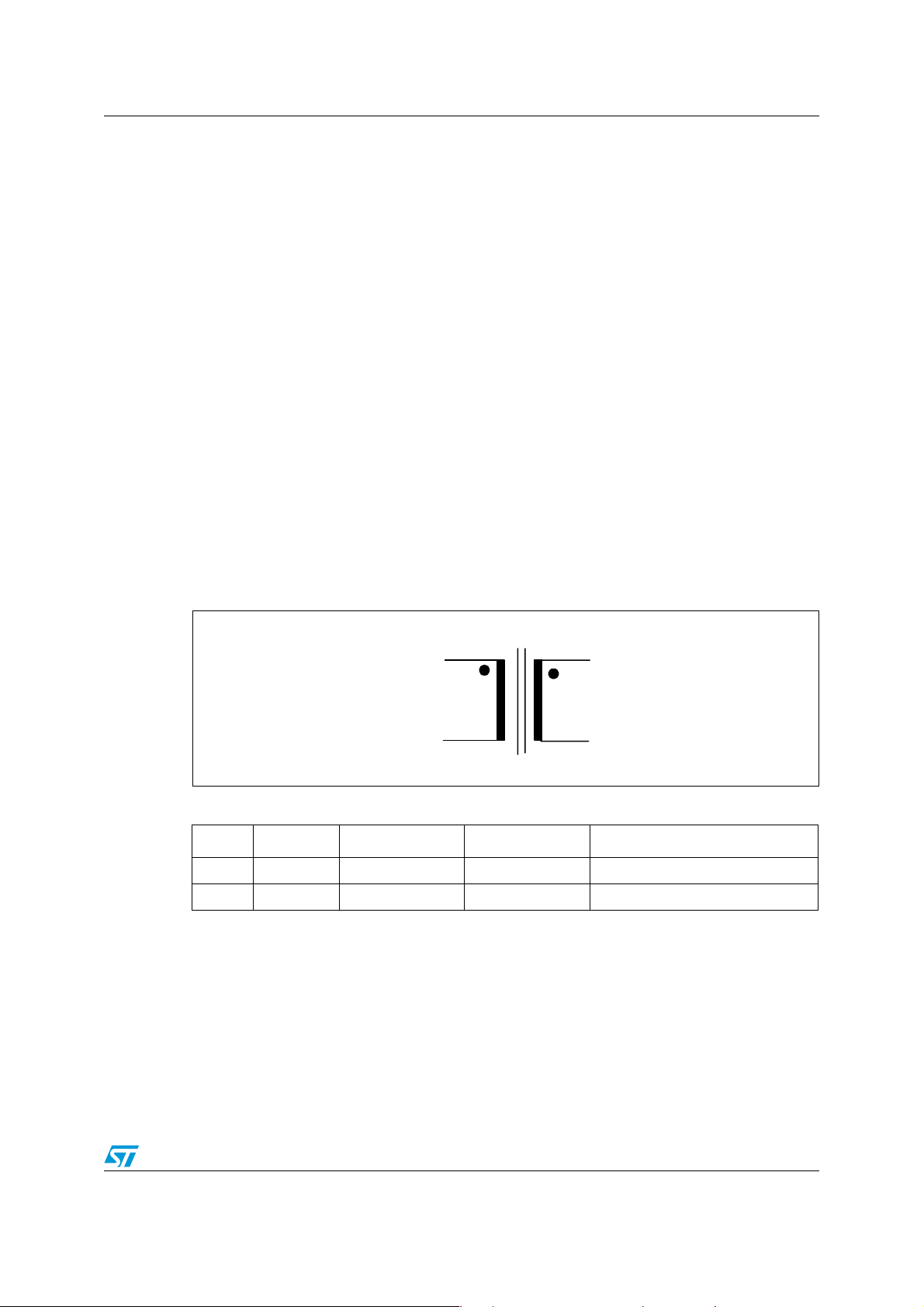
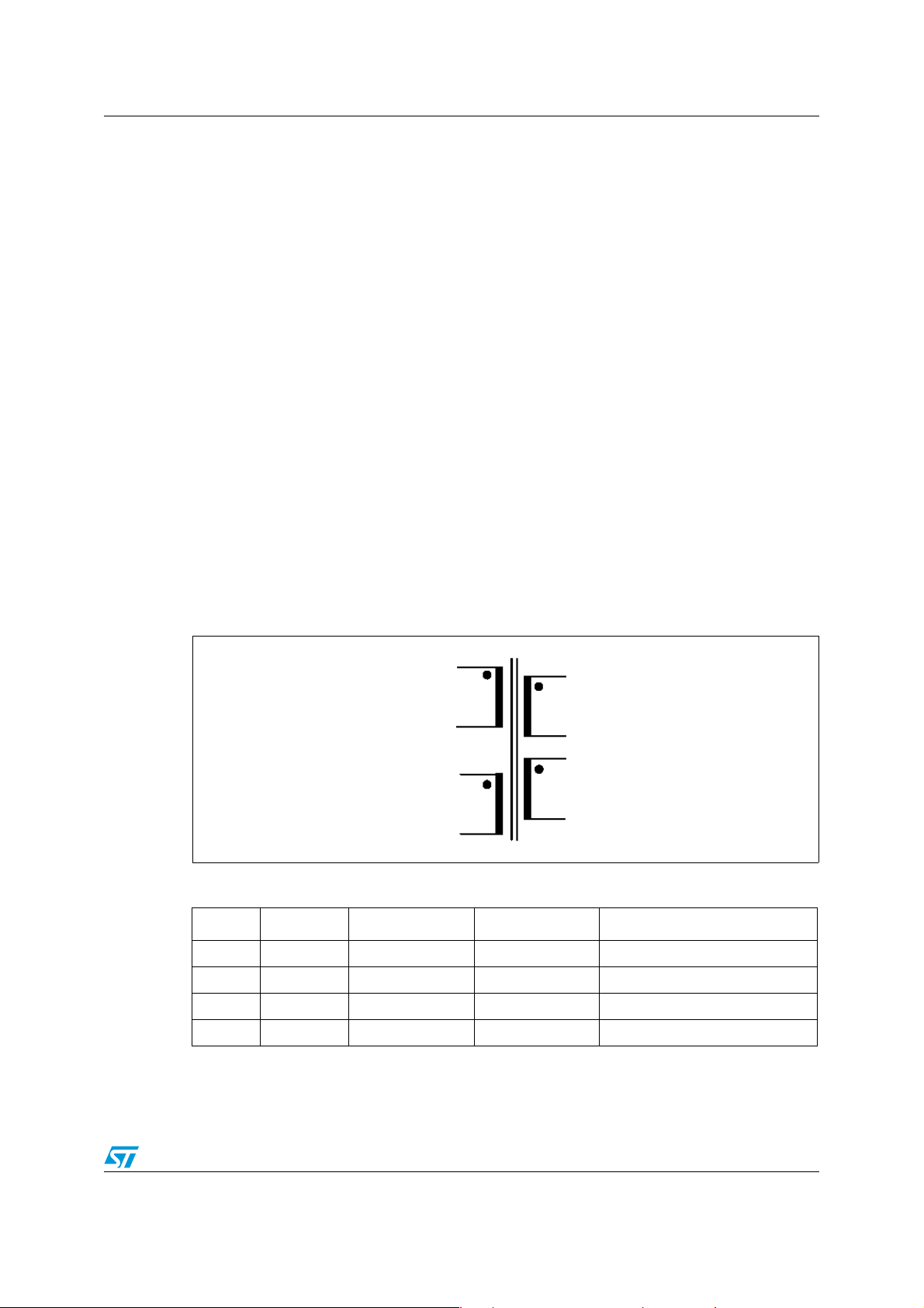
Figure 18. Electrical diagram . . . . . . . . . . . . . . . . . . . . . . . . . . . . . . . . . . . . . . . . . . . . . . . . . . . . . . . . 23
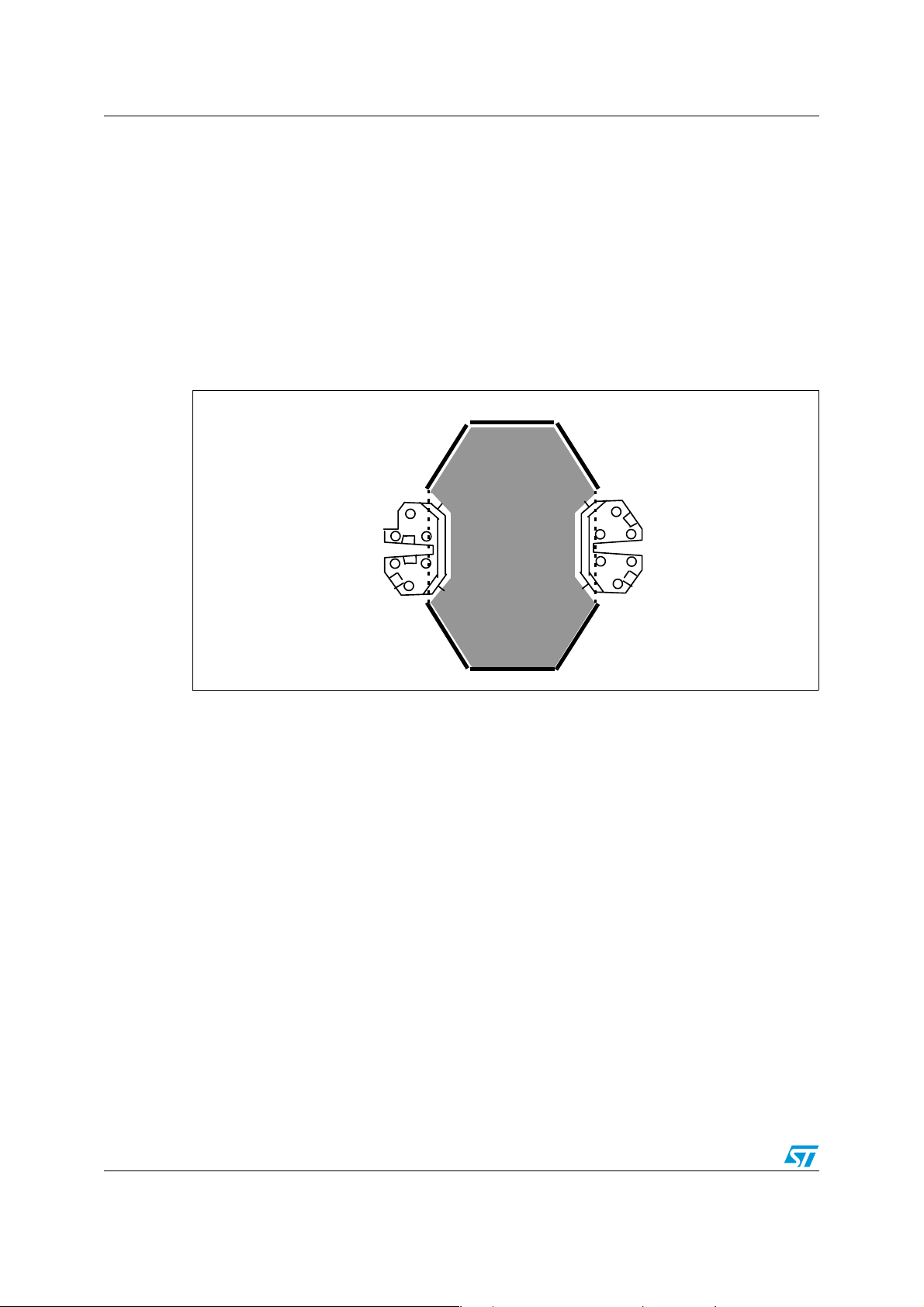
Figure 19. Bottom view . . . . . . . . . . . . . . . . . . . . . . . . . . . . . . . . . . . . . . . . . . . . . . . . . . . . . . . . . . . . 24
Figure 20. Electrical diagram . . . . . . . . . . . . . . . . . . . . . . . . . . . . . . . . . . . . . . . . . . . . . . . . . . . . . . . . 25
Figure 21. Pin lay-out, top view . . . . . . . . . . . . . . . . . . . . . . . . . . . . . . . . . . . . . . . . . . . . . . . . . . . . . . 26
Figure 22. Thru-hole component placing and top silk screen . . . . . . . . . . . . . . . . . . . . . . . . . . . . . . . 27
Figure 23. SMT component placing and bottom silk screen . . . . . . . . . . . . . . . . . . . . . . . . . . . . . . . . 27
Figure 24. Copper tracks . . . . . . . . . . . . . . . . . . . . . . . . . . . . . . . . . . . . . . . . . . . . . . . . . . . . . . . . . . . 27
4/29
Page 5

AN2321 Main characteristics and circuit description
1 Main characteristics and circuit description
The main characteristics of the SMPS are listed here below:
● Universal inpu t mains range: 90÷264 Vac - frequency 45 to 65 Hz
● Output v oltage: 19 V@4.7 A continuous operation
● Mains harmonics: Compliance with EN61000-3-2 specifications
● Standby mains consumption: Typ. 0.4 W @230 Vac; Max 0.5 W @265 Vac
● Overall efficiency: better than 90%
● EMI: Compliance with EN55022-class B specifications
● Safety: Compliance with EN60950 specifications
● Low profile design: 25 mm maximum height
● PCB single layer: 78x174 mm, mixed PTH/SMT technologies
The circuit consists of two stages: a front - end PF C imp l eme nt ing the L65 63 and a r eson ant
DC/DC converter based on the new resonant controller, the L6599. The Power Factor
Corrected (PFC) stage delivers a stable 400 VDC and provides for the reduction of the
mains harmonic, allowing to meet European standard EN61000-3-2. The controller is the
L6563 (U1), working in transition mode and integrating all functions needed to control the
PFC and interface the downstream resonant converter. The power stage of the PFC is a
conventional boost converter, connected to the output of the rectifier bridge. It includes coil
L2, diode D4 and capacitor C9. The boost s witch is re presented by the po w er MOSFET Q1.
The L2 secondary winding (pins 8-10) is dedicated to provide to the L6563 the information
about the PFC coil core demagnetization, necessary to the controller for the TM operation.
The divider R1, R2 and R14 provides to the L6563 the information of the instantaneous
voltage that is used to modulate the boost current, and to derive some further information
like the average value of the AC line, used by the V
function keeps the ou tput voltage almost independent of the mains on e . The divide r R7, R8 ,
R9, R10 detects the output voltage . The second divider R11, R12, R13 and R28 protects the
circuit in case of voltage loop fail. The second stage is a resonant converter, half bridge
topology, working in ZVS. The controller is the new L6599, incorporating the necessary
functions to drive properly the Half-bridge by a 50 percent fixed duty cycle with dead-time,
working with variable frequency.
(voltage feed-forward) function. This
FF
The main features of the L6599 are a non-linear soft-start, a new current protection pin
(ISEN, pin 6) that programs the hiccup mode timing, a dedicat ed pin for sequencing or
brown-out (LINE) and a stand-by pin (STBY) for burst mode operation at light load. The
transformer uses the integrated magnetic approach, incorporating the resonant series
inductance. Thus, no any external additional coil is needed for the resonance. The
transformer configuration chosen for the secondary winding is centre tap, using two
Schottky rectifiers, type STPS10L60FP. The feedback loop is implemented by means of a
typical circuit using a TL431 modifying the current in t he optocoupler diode . The optocoupler
transistor modulates the current from pin 4, so the frequency will change accordingly, thus
achieving the output voltage regulation. Resistor R34 sets the maximum operating
frequency and the load at which the controller starts to work in Burst mod e. In case of a
short circuit, the current into the primary winding is detected by the lossless circuit R41,
C27, D11, D10, R39, and C25 and it is fed into the pin 6. In case of o v erload, th e v oltage on
pin #6 will overpass an internal threshold that will trigger a protection sequence via pin #2,
keeping the current flo wing in the circuit at a safe lev el. In case of output v oltage loo p f ailure,
the intervention of the zener diode connected to pin #8 (DIS) will activate the latched
protection of the L6599. The DIS pin can be also activated by the L6563 via the
PWM_LATCH pin in case of PFC loop failure.
5/29
Page 6
Main characteristics and circuit description AN2321
Figure 1. Electrical diagram
+19V
RTN
J2
1
2
C32
100N
C31
L3
2u2
100uF-35V YXF
C21
C20
2N2 - Y1
R11
3M0
R12
3M0
R13
5K1
R28
27K
R7
1M0
R8
1M0
R10
15K
R9
82K
C9
R6
NTC_1 0R S23 6
47uF-450V
D4
STTH2L06
D3
1N4005
2-35
L2
86A-5158C
810
R3
2M4
D1
GBU4J
C5
470N-400V
R69
4K7
D20
BZV55- B15
Q9
BC847C
D7
LL4148
R70
100K
R71
Q10
R4
2M4
Q8
6K8
BC847C
D16
D17
BZV55 -B1 2
LL4148
STQ1HNK60R
R20
10K
2N2 - Y1
C18
2u2-6.3V
R44
2K7
R101
R19
56K
C39
100N
R66
2K2
Q6
BC847C
Q5
BC847C
R65
+19V@4.7A
D18
U2
*
39R
47K
D15
BZV5 5-C18
R56
1K8
R62
4K7
470uF-35V YXF
C30
470uF-35V YXF
C29
STPS10L60FP
D12
13
14
2
Q3
STP9NK50Z
LL4148
C19
100N
16
VBOOT
L6599D
CSS
1
Q1
4
C26
R58
100K
10uF-50V
R25
56R
13
14
15
NC
OUT
HVG
CF
DELAY
3
2
4
C45
220NF
C17
470PF
R24
1M0
R31
R30
STP12 NM50 FP
R46
100K
R27
470R
R21
39R
D13
STPS10L60FP
11
12
5
C28
22N
R59
100K
Q4
STP9N K50Z
R38
56R
C40
100N
D19
11
10
12
VCC
LVG
GND
LINE
STBY5RFmin
ISEN
7
6
R34
3K3
15K
10R
R23
R22
C43
0R47
0R47
C16
2N2
R49
39K
R43
51R
C36
1uF-50V
R42
5K6
T1
86A-5166A
6
R41
100R
C27
220PF
D10
LL4148
LL4148
4N7
D11
LL4148
9
R39
130R
PFC_STOP
C25
DIS
8
100N
C44
3N9
R32
47R
D8
BZV55 -B2 4
R29
1K0
R47
1K0
12
43
R60
10K
C23
10N
Q2
BC847C
R51
120K
R50
6K2
R48
47K
C34
220N
U4
TL431AIZ
U3
SFH617A-2
R40
6R8
D9
LL4148
220uF-35V
C24
R35
0R0
R37
100K
R52
6K8
C15
C4
470N-X2
L1
86A-5163
C3
C2
2N2
F1
FUSE 4A
1
J1
INPUT CONN.
2N2
C1
470N-X2
2
3
R1
1M0R21M2
90-264Vr ms
10uF-50V
U1
L6563
C14
100N
6/29
14
VCC
INV
1
C13
1uF
11
13
12
GD
ZCD
RUN
GND
MULT
COMP
3
2
R18
56K
PWM_STOP
PWM_LATCH
C10
PFC_OK
VFF5CS
TBO
4
C11
R14
18K
7
6
C12
470N
10N
150K
R15
22N
C22
220PF
R26
240K
*: R101 MOUNTED BY REWORKING
8
10
9
Page 7

AN2321 Test results
2 Test results
2.1 Efficiency measurements
Table 1 and Table 2 show the output voltage measurements at nominal mains with different
load conditions. Efficiency is then calcu lated . For all measurements, both at full load and no
load operation, the input pow er has been mea sured b y a digita l po wer meter, Yokogawa WT-
210. Particular attention has to be paid when measuring input power at full load in order to
avoid measurem ent errors due to the voltage drop on cables and connections. Therefore
please connect the WT210 voltmeter termination to the board inpu t connector . F or the same
reason please measure the output voltage at the output connector or use th e r emot e d etect
option of your active load for a correct voltage measurement.
Table 1. Efficiency measurements -
Vout [V] Iout [A] Pout [W] Pin [W] Efficiency (%)
18.95 4.71 89.25 99.13 90.04
18.95 3.72 70.49 78.00 90.38
18.97 2.7 51.22 56.55 90.57
18.98 1.71 32.46 36.00 90.16
18.99 1.0 18.99 21.70 87.51
18.99 0.5 9.50 11.30 84.03
Vin=115 Vac
19.00 0.25 4.75 5.86 81.06
Table 2. Efficiency measurements - Vin=230 Vac
Vout [V] Iout [A] Pout [W] Pin [W] Efficiency (%)
18.95 4.71 89.25 97.23 91.80
18.96 3.72 70.53 76.74 91.91
18.97 2.7 51.22 55.85 91.71
18.98 1.71 32.46 35.57 91.24
18.99 1.0 18.99 21.30 89.15
19.00 0.5 9.50 10.87 87.40
19.00 0.25 4.75 5.77 82.32
In Table 1, Table 2 and Figure 2, the overall circuit efficiency is measured at different loads,
powering the board at the tw o nominal input mains v oltages. The measures hav e been do ne
after 30 minutes of warm-up at maximum load. The high efficiency of the PFC working in
transition mode and the very high efficiency of the resonant stage w orking in ZVS , provides
for an overall efficiency better than 90%. This is a significant high number for a two-stage
converter delivering an output current of 4.7 amps, especially at low input mains voltage
where the PFC conduction losses increase. Even at lower loads, the efficiency remains still
high.
7/29
Page 8
Test results AN2321
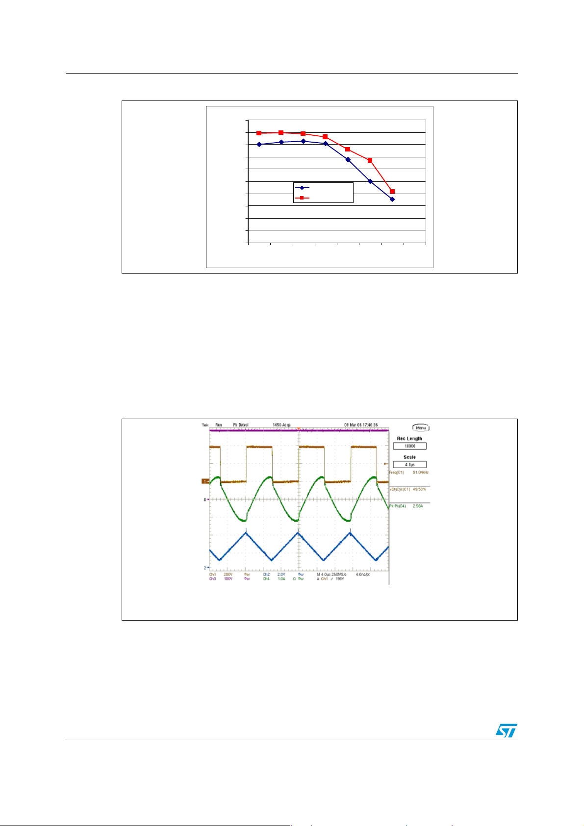
Figure 2. Efficiency vs. Pout
Effi ci en cy v s P out
Eff. @115Vac
Eff. @230Vac
O/P P o wer
Efficiency
94.00
92.00
90.00
88.00
86.00
84.00
82.00
80.00
78.00
76.00
74.00
89 71 51 32 19 10 5
The global efficiency at full load has been measured with good results even at the limits of
the input voltage range :
Vin = 90Vac - full load
Pin = 100.5 W
Efficiency = 88.9%
Vin = 264 Vac - Full load
Pin = 96.3 W
Efficiency = 92.6%
2.2 Resonant stage operating waveforms
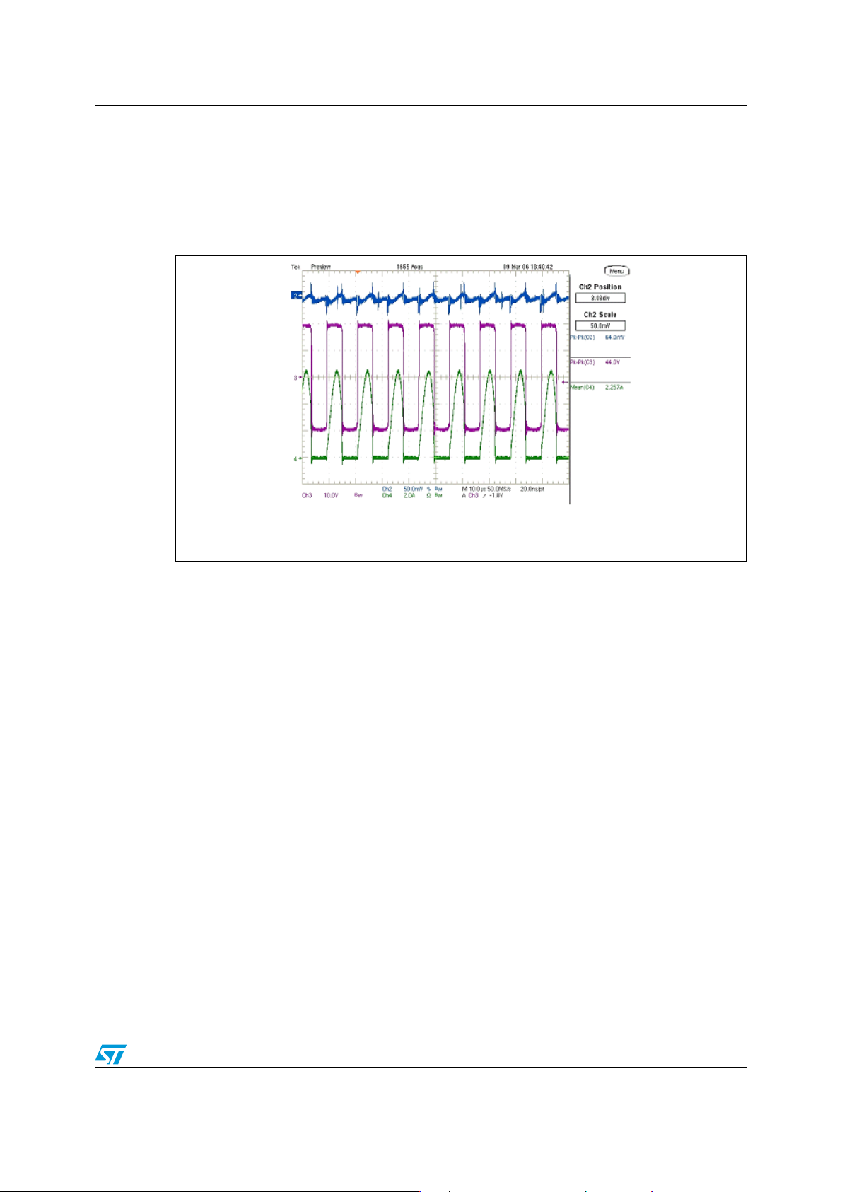
Figure 3. Resonant circuit primary side waveforms
CH1: L6599 - V
CH2: L6599 - V
(HB voltage)
PIN14
(CF)
PIN3
CH3: +400 V PFC Output voltage
CH4: T1 primary winding current
In Figure 3 are reported some waveforms during steady state operation of the circuit at full
load. The CH2 waveform is the oscillator signal at pin #3 of the L6599, while the CH3
waveform is the PFC output voltage , po wering th e resonant stage . The CH1 tra ce is the ha lf
bridge waveform, driving the resonant circuit. In the picture it is not obvious, but the
switching frequency is normally slightly modulated following the PFC 100 Hz ripple that is
rejected by the resonant control circuitry. The switching frequency has been chosen around
90 kHz, in order to have a good trade off between transformer losses and its dimensions.
8/29
Page 9
AN2321 Test results
The transformer primary current wave shape is the CH4 trace. As shown, it is almost
sinusoidal, because the operating frequency is slightly above the resonance of the leakage
inductance and the resonant capacitor (C28).
In this condition, the circuit has a good margin for ZVS operations providing good efficiency
and the almost sinusoidal wave shape provides for an extremely low EMI generation.
Figure 4. Resonant circuit secondary side waveforms
CH2: +19V Output voltage ripple and noise
CH3: D12 rectifiers anode voltage
CH4: D12 rectifiers current
In Figure 4 are represented some waveforms relevant to the secondary side: the rectifiers
reverse voltage is measured by CH3 and the peak to peak value is indicated on the right of
the picture. It is a bit higher than the theoretical value that would be 2(V
about 40 V. It is possible to observe a small ringing on the bottom side of the waveform,
responsible for this difference. The channel CH4 (green in the picture) shows the current in
the diode D12, equal to that one flowing in D13. Even this current shape is almost a sine
wave, its average value is half of the output current. The ripple and noise on the output
voltage is measured by CH2.
Thanks to the advantages of the resonant converter, the high frequency ripple and noise of
the output voltage is o nly 100mV (0.52%) including spik es, whi le the resi dual ripple at mains
frequency is 130 mV at maximum load and any line condition.
2.3 Stand-by & no load power consumption
The board is specifically designed for li ght load and zero load operation, like during
operation with load disconnected. The result s are reported in the diagram of Figure 5, he re
following. As high lighted in the diagram of Figure 4, the input power at no load is always
below 0.4 W for any input mains voltage. Thanks to the L6599 stand-by function, at light load
conditions both the resonant converter and the PFC work skipping switching cycles,
according to the load. In fact, the L6599 via the PFC_ST OP pin (#9) stops the operation of
the L6563 during the burst mode off-time.
OUT+VF
), hence
9/29
Page 10

Test results AN2321
Figure 5. Input power without load vs. mains voltage
Pin vs. Vac @ no- l oad
0.5
0.4
0.3
0.2
Input power
0.1
0
90Vac 115Vac 230Vac 265Vac
Pin= [W]
0.4 0.28 0.34 0.37
Mains voltage
The result is visible in Figure 6: the two converters are now working for a very short time, the
output voltage is perf ectly regula ted at its nominal v alue , with just a negligib le residual ripple
over imposed (~14 0mV). Thanks to the burst mode and the reduced number of switching
cycles the relevant losses are drastically reduced, therefore input power drawn from the
mains is very low . How e v er , if the ou tput v oltage has a sudden load change , both con v erters
are ready to react immediately, thus avoiding output v oltage drops. In Figure 7 the details of
the wav eforms captured in Figure 6 show some details during the switching period and
additionally, the L6563 RUN pin (#10) signal is captured. This pin is connected to the
PFC_STOP pin (#9) of the L6599 and enables the operation of the PFC during the burst
pulse of the resonant.
Figure 6. Waveforms at no-load operation Figure 7. Waveforms at no-load operation
CH1: L6599 - V
CH2: +19 V Output voltage
(HB voltage)
PIN14
CH3: +400 V PFC Output voltage
CH4: Q1-Drain voltage
Table 3 and Table 4 report the measurements of the input power during operation as a
function of the output power. Even with reduced load operation, the burst mode functio nality
allows to work with good circuit efficiency.
10/29
CH1: L6599 - V
CH2: L6563 - V
CH3: +400 V PCF Output voltage
(HB voltage)
PIN14
(RUN pin)
PIN10
CH4: Q1 - Drain voltage
Page 11

AN2321 Test results
Table 3. Stand-by consumption - Vin=115 Vac
Vout [V] Iout [mA] Pout [W] Pin [W]
19.01 80 1.5 3
19.01 53 1 2
19.01 27 0.5 1.08
19.01 13 0.25 0.66
Table 4. Stand-by consumption - Vin=230 Vac
Vout [V] Iout [mA] Pout [W] Pin [W]
19.01 80 1.5 2.4
19.01 53 1 1.68
19.01 27 0.5 1
19.01 13 0.25 0.67
Figure 8 shows the waveforms of the outpu t v oltage and current during a load v ariation from
0 to 100%. During operation at zero load, the circuit is w orking in burst mode as described
before then, as soon as the load incr eases it works in continuous switching operation. As
shown, due to the fact that the PFC is always operating, the circuit response is fast enough
to avoid outp ut vo ltage dips . In Figure 9, the opposite load transition is ch eck e d (100% to 0 ).
Even in this case the tr ansition in clean and doesn 't show any prob lem f or th e output v olt age
regulation.
Thus, it is clear that the proposed architecture is the most suitable for power su pply
operating with strong load variation without any problem related to the load regulation.
Figure 8. Load transition 0 ÷ 100% Figure 9. Load transition 100% ÷ 0
CH3: +19 V Output voltage
CH4: +19 V Output current
CH3: +19 V Output voltage
CH4: +19 V Output current
11/29
Page 12

Test results AN2321
2.4 Short circuit protection
The L6599 is equipped with a current sensing input (pin #6, ISEN) and a dedicated over
current management system. The current flowing in the circuit is detected and the signal is
fed into the ISEN pin. It is internally connected to the input of a first comparator, referenced
to 0.8 V, and to that of a second comparator referenced to 1.5 V. If the voltage externally
applied to the pin by either circuit in Figure 8 exceeds 0.8 V, the first comparator is tripped
causing an internal switch to be turne d on and dis c ha r ging th e sof t- s ta rt capacitor CSS.
Under output short circuit, this operation results in a nearly constant peak primary current.
With the L6599 the designer can progra m externally the maximum time (TSH) that the
converter is allowed to run overloaded or under short circuit conditions. Overloads or short
circuits lasting less than TSH will not cause any other action, hence providing the system
with immunity to short duration phenomena. If, instead, TSH is exceeded, an overload
protection (OLP) procedure is activated that shuts down the L6599 and, in case of
continuous overload/short circuit, results in continuous intermittent operation with a userdefined duty cycle. This function is realized with the pin DELAY (#2), by means of a
capacitor C45 and the parallel resistor R24 connected to ground. As the voltage on the
ISEN pin exceeds 0.8V t he first OCP comparator, in addition to discharging CSS, turns on
an internal current generator that via the DELA Y pin charges C45. As the voltage on C45 is
3.5 V, the L6599 sto p s switching and the PFC_STOP pin is pulled low. Also the internal
generator is turned off, so that C45 will now be slowly discharged by R24. The IC will restart
when the voltage on C45 will be less than 0.3 V. Additionally, if the voltage on the ISEN pin
reaches 1.5 V for any reason (e.g. transformer saturation), the second comparator will be
triggered, the L6599 will shutdown and the operation will be resumed after an on-off cycle.
Figure 10. O/P short circuit waveforms Figure 11. O/P short circuit waveforms
(zoomed)
CH1: L6599 - V
CH2: L6599 - V
CH3: L6599 - V
CH4: Output current
#14 (HB voltage)
PIN
#2 (DELAY)
PIN
#6 (ISEN)
PIN
The L6599 short circuit protection sequence described above is visib le in the Figure 10. The
on/off operation is controlled by the voltage on pin #2 (DELAY), providing for the hiccup
mode of the circuit.
Thanks to this control pin, the designer can select the hiccup mode timing and th us keep the
average output current at a safe lev el. Please note on the picture left side the very low mean
current flowing in the shorted output, less than 0.3 A. A better detail of the waveforms can
12/29
CH2: L6599 - V
CH3: L6599 - V
CH4: Output current
PIN
PIN
#2 (DELAY)
#6 (ISEN)
Page 13

AN2321 Test results
be appreciated in Figure 11 where it is possible to recognize the oper ation phases
described above.
2.5 Over voltage protections
Both circuit stages, PFC and resonant, are equipped with their own over voltage protection.
The PFC controller L6563 is internally equipped with a dynamic and a static over voltage
protection circuit detecting the error amp lifie r via th e voltage divider de d icat ed to th e
feedback loop to detect the PFC output voltage. In case the internal threshold is exceeded,
the IC limits the voltage to a programmable, safe value. Moreover , in the L6563 there is an
additional protection against loop failures using an additional divider (R11, R12, R13, R28)
connected to a dedicated pin (PFC_OK, #7) protecting the circuit in case of loop failures,
disconnection or deviation from the nominal value of the feedback loop divider. Hence the
PFC output voltage is always under control and in case a fault condition is detected the
PFC_OK circuitry will latch the L6563 operations and, by means of the PWM_LATCH pin
(#8) it will latch the L6599 as well via the pin #8 (DIS).
The pin DIS is also used to protect the resonant stage against over voltage or loop
disconnections. In fact, the zener diode D8 connected to pin DIS detects the voltage and in
case of open loop it will conduct and voltage on pin DIS will exceed the internal threshold.
Then the IC will be immediately shut down and its consumption reduced at a low value. This
state will be latched and will be necessary to let the voltage on the Vcc pin go below the
UVLO threshold to reset the latch and restart the IC operation.
2.6 Start-up sequence
Figure 12. Start-up @115 Vac - full load Figure 13. Start-up @115 Vac - full load
CH1: L6599 - V
CH2: Vcc voltage
CH3: +19 V Output voltage
CH4: +400 V PFC Output voltage
(HB voltage)
PIN14
Figure 12 shows the wavef orms during the start at 90 V a c and full load . It is possib le t o note
the sequence of the two sta ges: at po wer on the L6563 and L6599 Vcc v o ltages increase up
to the turn-on thresholds of the two ICs. The PFC starts and its output voltage increases
from the mains rectified voltage to its nominal value, with a small ov ershoot. In the meantime
the L6599 is kept inactive by the LINE pin (#7) until the PFC voltage reaches the threshold
CH1: L6599 - V
CH2: L6599 - V
CH3: +19 V Output voltage
CH4: Resonant capacitor C28 current
(HB voltage)
PIN14
(SS)
PIN2
13/29
Page 14

Test results AN2321
set by the divider R11, R12, R13, R28. As so on as it reaches th e L6599 LINE pin th reshold,
the resonant starts to operate. Hence the output voltage rises according to the soft-start and
reaches the nominal level. This sequence provides for the advantages of a perfect
sequencing of the circuit at start-up with the PFC acting as master and avoids complex
additional circuitry for the correct start-up of the circuit in all conditio ns. T he circuit has been
tested in all line and load conditions showing a correct start-up sequence. The used hi gh
voltage start-up circuit used avoids useless po wer dissipation during light load operation and
provides for an almost constant wake-up time of the circuit.
In Figure 13, the L6599 start-up sequence is analyzed: as soon as the LINE pin (#7)
enables the operation of the L65 99 co nverter's soft start-up sequence is triggered therefore
initially, the capacitor C18 is totally discharged, and the resistor R44 is effectively in parallel
to R24 thus the resulting initial frequency is determined by R
and R
SS
only, since the
Fmin
optocoupler's phototransistor is off ( as long as the output v oltage is not too f ar a wa y from the
regulated value). C18 is progressively charged until its voltage reaches the reference
voltage (2 V) and, consequently, the current through R44 goes to zero.
During this frequency sweep the operating frequency will decrease follo wing the exponential
charge of C18 that will count balance the non-linear frequency dependence of the tank
circuit. As a result, the average input current will smoothly increase , without the peaking that
occurs with linear frequency sweep, and the output voltage will reach the regulated value
with almost no overshoot as the waveforms in the picture.
14/29
Page 15

AN2321 Thermal tests
3 Thermal tests
In order to check the design reliability, a thermal mapping by means of an IR Camera was
done. Here below the thermal measures of the board, component side, at nominal input
voltage are shown. Some pointers visible on the pictures have been placed across key
components or components showing high temperature. The correlation between
measurement points and components is indicated below, for both diagrams.
Figure 14. Thermal map @115 Vac - full load
Table 5. Temperature of measured points @115 Va c - full load
Points - ref. Temp
A - D1 59.1 °C
B - Q1 54.0 °C
C - D4 67.6 °C
D - R6 85.8 °C
E - L2 45.7 °C
F - Q4 46.2 °C
G - Q3 46.5 °C
H - T1
CORE
I - T1
PR
J - T1
SEC
K - D12 62.8 °C
L - D13 62.8 °C
61.8 °C
67.2 °C
67.4 °C
T
AMB
=27°C
15/29
Page 16

Thermal tests AN2321
Figure 15. Thermal map @230 Vac - full load
T
=27°C
AMB
Table 6. Temperature of measured points @230Vac - full load
Points - ref. Temp
A - D1 45.9 °C
B - Q1 44.3 °C
C - D4 59.0 °C
D - R6 72.4 °C
E - L2 43.7 °C
F - Q4 46.8 °C
G - Q3 46.5 °C
H - T1
I - T1
J - T1
CORE
PR
SEC
63.7 °C
67.9 °C
69.5 °C
K - D12 64.8 °C
L - D13 64.9 °C
All other components of the board are working within the temperature limits, assuring a
reliable long term operation of the power supply.
16/29
Page 17

AN2321 Conducted emission pre-compliance test
4 Conducted emission pre-compliance test
The limits indicated on both diagrams at 115 Vac and 230 Vac comply with EN55022 ClassB specifications. The values are measured in peak detection mode.
Figure 16. CE peak measure at 115 Vac and full load
115Vac
FULL LOAD
Figure 17. CE peak measure at 230 Vac and full load
230 Vac
FULL LOAD
17/29
Page 18

Bill of material AN2321
5 Bill of material
Table 7. Bill of material
Res.
des.
C1 470N-X2 X2 FILM CAPACITOR - R46-I 3470--M1- RUBYCON
C1 470N-X2 X2 FILM CAPACITOR - R46-I 3470--M1- ARCOTRONICS
C10 22N 50 V CERCAP - GENERAL PURPOSE AVX
C11 10N 50 V CERCAP - GENERAL PURPOSE AVX
C12 470N 25 V CERCAP - GENERAL PURPOSE AVX
C13 1uF 25 V CERCAP - GENERAL PURPOSE AVX
C14 100N 50 V CERCAP - GENERAL PURPOSE AVX
C15 10uF-50V ALUMINIUM ELCAP - YXF SERIES - 105 °C RUBYCON
C16 2N2 50 V CERCAP - GENERAL PURPOSE AVX
C17 470PF 50 V - 5% - C0G - CERCAP AVX
C18 2 µF2-6.3 V 25 V CERCAP - GENERAL PURPOSE AVX
C19 100N 50 V CERCAP - GENERAL PURPOSE AVX
C2 2N2 Y1 SAFETY CAP. MURATA
C20 2 N2 - Y1 DE1E3KX222M - Y1 SAFETY CAP. MURATA
C21 2 N2 - Y1 DE1E3KX222M - Y1 SAFETY CAP. MURATA
C22 220PF 50 V CERCAP - GENERAL PURPOSE AVX
C23 10N 50 V CERCAP - GENERAL PURPOSE AVX
C24 220 µF-35 V ALUMINIUM ELCAP - YXF SERIES - 105 °C RUBYCON
Part type/
part value
Description Supplier
C25 100N 50 V CERCAP - GENERAL PURPOSE AVX
C26 10 µF-50 V A LUMINIUM ELCAP - YXF SERIES - 105 °C RUBYCON
C27 220PF 500 V CERCAP - 5MQ221KAAAA AVX
C28 22N 630 V - PHE450MA5220JR05 EVOX-RIFA
C29 470 µF-35 V YXF ALUMINIUM ELCAP - YXF SERIES - 105 °C RUBYCON
C3 2N2 Y1 SAFETY CAP. MURATA
C30 470 µF-35 V YXF ALUMINIUM ELCAP - YXF SERIES - 105 °C RUBYCON
C31 100 µF-35 V YXF ALUMINIUM ELCAP - YXF SERIES - 105 °C RUBYCON
C32 100N 50 V CERCAP - GENERAL PURPOSE AVX
C34 220N 50 V CERCAP - GENERAL PURPOSE AVX
C36 1 µF-50 V ALUMINIUM ELCAP - YXF SERIES - 105 °C RUBYCON
C39 100N 50 V CERCAP - GENERAL PURPOSE AVX
C4 470N-X2 X2 FILM CAPACITOR - R46-I 3470--M1- ARCOTRONICS
C40 100N 50 V CERCAP - GENERAL PURPOSE AVX
18/29
Page 19

AN2321 Bill of material
Table 7. Bill of material (continued)
Res.
des.
C43 4N7 50V CERCAP - GENERAL PURPOSE AVX
C44 3N9 50V CERCAP - GENERAL PURPOSE AVX
C45 220NF 25V CERCAP - GENERAL PURPOSE AVX
C5 470N-400 V PHE426KD6470JR06L2 - POLYPROP. FILM CAP EVOX-RIFA
C9 47 µF-450 V ALUMINIUM ELCAP - ED SERIES - 105°C PANASONIC
D1 GBU4J SINGLE PHASE BRIDGE RECTIFIER VISHAY
D10 LL4148 FAST SWITCHING DIODE VISHAY
D11 LL4148 FAST SWITCHING DIODE VISHAY
D12 STPS10L60FP POWER SCHOTTKY RECTIFIER STMicroelectronics
D13 STPS10L60FP POWER SCHOTTKY RECTIFIER STMicroelectronics
D15 BZV55-C18 ZENER DIODE VISHAY
D16 LL4148 FAST SWITCHING DIODE VISHAY
D17 BZV55-C12 ZENER DIODE VISHAY
D18 LL4148 FAST SWITCHING DIODE VISHAY
D19 LL4148 FAST SWITCHING DIODE VISHAY
D20 BZV55-B15 ZENER DIODE VISHAY
D3 1N4005 GENERAL PURPOSE RECTIFIER VISHAY
Part type/
part value
Description Supplier
D4 STTH2L06 ULTRAFAST HIGH VOLTAGE RECTIFIER STMicroelectronics
D7 LL4148 FAST SWITCHING DIODE VISHAY
D8 BZV55-B24 ZENER DIODE VISHAY
D9 LL4148 FAST SWITCHING DIODE VISHAY
F1 FUSE 4A FUSE T4A - TIME DELAY WICHMANN
HS1 HEAT SINK FOR D1&Q1 DWG
HS2 HEAT SINK FOR Q3&Q4 DWG
HS3 HEAT SINK FOR D12&D13 DWG
J1 MKDS 1,5/ 3-5,08 PCB TERM. BLOCK, SCREW CONN.- 3 W. PHOENIX CONTACT
J2 MKDS 1,5/ 2-5,08 PCB TERM. BLOCK, SCREW CONN.- 2 W. PHOENIX CONTACT
L1 86A-5163 INPUT EMI FILTER DELTA ELECTRONICS
L2 86A-5158C PFC INDUCTOR DELTA ELECTRONICS
L3 RFB0807-2R2 2u2 - RADIAL INDUCTOR COILCRAFT
Q1 STP12NM50FP N-CHANNEL POWER MOSFET STMicroelectronics
Q10 BC847C NPN SMALL SIGNAL BJT STMicroelectronics
Q2 BC847C NPN SMALL SIGNAL BJT STMicroelectronics
Q3 STP9NK50ZFP N-CHANNEL POWER MOSFET STMicroelectronics
19/29
Page 20

Bill of material AN2321
Table 7. Bill of material (continued)
Res.
des.
Q4 STP9NK50ZFP N-CHANNEL POWER MOSFET STMicroelectronics
Q5 BC847C NPN SMALL SIGNAL BJT STMicroelectronics
Q6 BC847C NPN SMALL SIGNAL BJT STMicroelectronics
Q8 STQ1HNK60R N-CHANNEL POWER MOSFET STMicroelectronics
Q9 BC847C NPN SMALL SIGNAL BJT STMicroelectronics
R1 1M0 SMD STANDARD FILM RES - 1/4 W - 5% - 250ppm/°C BC COMPONENTS
R10 15K SMD STANDARD FILM RES - 1/8 W - 1% - 100ppm/°C BC COMPONENTS
R11 3M0 MBB0207 AXIAL FILM RES - 0.4 W - 1% - 50ppm/°C BC COMPONENTS
R12 3M0 MBB0207 AXIAL FILM RES - 0.4 W - 1% - 50ppm/°C BC COMPONENTS
R13 8K2 SMD STANDARD FILM RES - 1/8 W - 1% - 100ppm/°C BC COMPONENTS
R14 18K SMD STANDARD FILM RES - 1/4 W - 5% - 250ppm/°C BC COMPONENTS
R15 150K SMD STANDARD FILM RES - 1/8 W - 5% - 250ppm/°C BC COMPONENTS
R18 56K SMD STANDARD FILM RES - 1/8 W - 5% - 250ppm/°C BC COMPONENTS
R19 56K SMD STANDARD FILM RES - 1/8 W - 5% - 250ppm/°C BC COMPONENTS
R2 1M2 SMD STANDARD FILM RES - 1/4 W - 5% - 250ppm/°C BC COMPONENTS
R20 10K SMD STANDARD FILM RES - 1/4 W - 5% - 250ppm/°C BC COMPONENTS
R21 39R SMD STANDARD FILM RES - 1/4 W - 5% - 250ppm/°C BC COMPONENTS
Part type/
part value
Description Supplier
R22 0R47
R23 0R47
R24 1M0 SMD STANDARD FILM RES - 1/4 W - 5% - 250ppm/°C BC COMPONENTS
R25 56R SMD STANDARD FILM RES - 1/8 W - 5% - 250ppm/°C BC COMPONENTS
R26 240K SMD STANDARD FILM RES - 1/8 W - 5% - 250ppm/°C BC COMPONENTS
R27 470R SMD STANDARD FILM RES - 1/4 W - 5% - 250ppm/°C BC COMPONENTS
R28 24K9 SMD STANDARD FILM RES - 1/8 W - 1% - 100ppm/°C BC COMPONENTS
R29 1K0 SMD STANDARD FILM RES - 1/4 W - 5% - 250ppm/°C BC COMPONENTS
R3 2M4 SMD STANDARD FILM RES - 1/4 W - 5% - 250ppm/°C BC COMPONENTS
R30 10R SMD STANDARD FILM RES - 1/8 W - 5% - 250ppm/°C BC COMPONENTS
R31 15K SMD STANDARD FILM RES - 1/8 W - 1% - 100ppm/°C BC COMPONENTS
R32 47R SMD STANDARD FILM RES - 1/4 W - 5% - 250ppm/°C BC COMPONENTS
R34 3K3 SMD STANDARD FILM RES - 1/4 W - 5% - 250ppm/°C BC COMPONENTS
R35 0R0 SMD STANDARD FILM RES - 1/8 W - 5% - 250ppm/°C BC COMPONENTS
R37 100K SMD STANDARD FILM RES - 1/4 W - 5% - 250ppm/°C BC COMPONENTS
R38 56R SMD STANDARD FILM RES - 1/8 W - 5% - 250ppm/°C BC COMPONENTS
SFR25 AXIAL STAND. FILM RES - 0.4 W - 5% 250ppm/°C
SFR25 AXIAL STAND. FILM RES - 0.4 W - 5% 250ppm/°C
BC COMPONENTS
BC COMPONENTS
20/29
Page 21

AN2321 Bill of material
Table 7. Bill of material (continued)
Res.
des.
R39 130R SMD STANDARD FILM RES - 1/4 W - 5% - 250ppm/°C BC COMPONENTS
R4 2M4 SMD STANDARD FILM RES - 1/4 W - 5% - 250ppm/°C BC COMPONENTS
R40 6R8
R41 100R
R42 5K6 SMD STANDARD FILM RES - 1/4 W - 5% - 250ppm/°C BC COMPONENTS
R43 51R SMD STANDARD FILM RES - 1/8 W - 5% - 250ppm/°C BC COMPONENTS
R44 2K7 SMD STANDARD FILM RES - 1/4 W - 5% - 250ppm/°C BC COMPONENTS
R46 100K SMD STANDARD FILM RES - 1/8 W - 5% - 250ppm/°C BC COMPONENTS
R47 1K0 SMD STANDARD FILM RES - 1/8 W - 5% - 250ppm/°C BC COMPONENTS
R48 47K SMD STANDARD FILM RES - 1/8 W - 5% - 250ppm/°C BC COMPONENTS
R49 39K SMD STANDARD FILM RES - 1/4 W - 5% - 250ppm/°C BC COMPONENTS
R50 6K2 SMD STANDARD FILM RES - 1/8 W - 1% - 100ppm/°C BC COMPONENTS
R51 120K SMD STANDARD FILM RES - 1/8 W - 1% - 100ppm/°C BC COMPONENTS
R52 6K8 SMD STANDARD FILM RES - 1/4 W - 5% - 250ppm/°C BC COMPONENTS
R53 0R0 0R0 JUMPER BC COMPONENTS
Part type/
part value
Description Supplier
SFR25 AXIAL STAND. FILM RES - 0.4 W - 5% 250ppm/°C
SFR25 AXIAL STAND. FILM RES - 0.4 W - 5% 250ppm/°C
BC COMPONENTS
BC COMPONENTS
R54 0R0 0R0 JUMPER BC COMPONENTS
R55 0R0 0R0 JUMPER BC COMPONENTS
R56 1K8 SMD STANDARD FILM RES - 1/8 W - 5% - 250ppm/°C BC COMPONENTS
R57 0R0 0R0 JUMPER BC COMPONENTS
R58 100K SMD STANDARD FILM RES - 1/8 W - 5% - 250ppm/°C BC COMPONENTS
R59 100K SMD STANDARD FILM RES - 1/8 W - 5% - 250ppm/°C BC COMPONENTS
R6 NTC_10R S236 NTC RESISTOR P/N B57236S0100M000 EPCOS
R60 10K SMD STANDARD FILM RES - 1/4 W - 5% - 250ppm/°C BC COMPONENTS
R62 4K7 SMD STANDARD FILM RES - 1/8 W - 5% - 250ppm/°C BC COMPONENTS
R65 47K SMD STANDARD FILM RES - 1/8 W - 5% - 250ppm/°C BC COMPONENTS
R66 2K2 SMD STANDARD FILM RES - 1/4 W - 5% - 250ppm/°C BC COMPONENTS
R69 4K7 SMD STANDARD FILM RES - 1/8 W - 5% - 250ppm/°C BC COMPONENTS
R7 1M0 MBB0207 AXIAL FILM RES - 0.4 W - 1% - 50ppm/°C BC COMPONENTS
R70 100K SMD STANDARD FILM RES - 1/8 W - 5% - 250ppm/°C BC COMPONENTS
R71 12K SMD STANDARD FILM RES - 1/4 W - 1% - 100ppm/°C BC COMPONENTS
R72 0R0 0R0 JUMPER BC COMPONENTS
R8 1M0 MBB0207 AXIAL FILM RES - 0.4 W - 1% - 50ppm/°C BC COMPONENTS
R9 82K SMD STANDARD FILM RES - 1/8 W - 1% - 100ppm/°C BC COMPONENTS
21/29
Page 22

Bill of material AN2321
Table 7. Bill of material (continued)
Res.
des.
R101
(1)
Part type/
part value
Description Supplier
39R SMD STANDARD FILM RES - 1/8 W - 5% - 250ppm/°C BC COMPONENTS
T1 86A-5166A RESONANT POWER TRANSFORMER DELTA ELECTRONICS
U1 L6563 TRANSITION-MODE PFC CONTROLLER STMicroelectronics
U2 L6599D HIGH VOLTAGE RESONANT CONTROLLER STMicroelectronics
U3 SFH617A-2 OPTOCOUPLER INFINEON
U4 TL431AIZ PROGRAMMABLE SHUNT VOLTAGE REFERENCE STMicroelectronics
1. R101 mounted by reworking on PCB
22/29
Page 23
AN2321 PFC coil specification
6 PFC coil specification
● Application type: consumer, IT
● Transformer type: open
● Coil former: vertical type, 6+6 pins
● Max. temp. rise: 45 °C
● Max. operating ambient temp.: 60 °C
● Mains insulation: N.A.
6.1 Electrical characteristics
● Converter topology: boost, transition mode
● Core type: RM14 - PC40 or equivalent
● Min. operating frequency: 20 kHz
● Primary inductance: 700 µH ±10% @1 kHz - 0.25 V (see Note 1)
● Peak primary current: 5 Apk
● RMS primary current: 1.8 A r ms
Note: 1 Measured between pins #2 & #5
Figure 18. Electrical diagram
Table 8. Winding characteristics
Pins Winding RMS current Number of turns Wire type
5 - 2 PRIMARY 1.8 A
8 - 11 AUX
1. Auxiliary winding is wound on top of primary winding
(1)
RMS
0.05 A
PRIM.
RMS
5
8
AUX
2
53 STRANDED 7 x φ 0.28 mm – G2
4 SPACED φ 0.28 mm – G2
11
23/29
Page 24
PFC coil specification AN2321
6.2 Mechanical aspect and pin numbering
● Maximum height from PCB: 22 mm
● Coil former type: vertical, 6+6 pins
● Pin distance: 5.08 mm
● Pins #1, 3, 4, 6, 7, 10, 12 are removed - Pin 9 is for polarity key.
● External copper shield: Bare, wound around the ferrite core and including the winding
and coil former. Height is 7 mm. Connected by a solid wire soldered to pin 11.
● Manufacturer: DELTA ELECTRONICS
● P/N: 86A - 5158C
Figure 19. Bottom view
2
x
x
x
x
5
8
x
9
x
x
10
11
24/29
Page 25
AN2321 Resonant power transformer specification
7 Resonant power transformer specification
● Application type: consumer, IT
● Transformer type: open
● Coil former: Horizontal type, 7+7 pins, 2 Slots
● Max. temp. rise: 45 °C
● Max. operating ambient temp.: 60 °C
● Mains insulation: Compliance with EN60950
7.1 Electrical characteristics
● Converter topology: half-bridge, resonant
● Core type: ER35 - PC40 or equivalent
● Min. operating frequency: 60 kHz
● Typical operating frequency: 100 kHz
● Primary inductance: 810 µH ±10% @1 kHz - 0.25 V (see Note 1)
● Leakage inductance: 200 µH ±10% @1 kHz - 0.25 V (see Note 1 and Note 2)
Note: 1 Measured between pins 1-4.
2 Measured between pins 1-4 with ONLY a secondary winding shorted.
Figure 20. Electrical diagram
Table 9. Winding characteristics
Pins Winding RMS current Number of turns Wire type
2 - 4 PRIMARY 1 A
14 - 13 SEC. A
12 - 11 SEC. B
5-6 AUX
1. Secondary windings A and B must be wound in parallel
2. Auxiliary winding is wound on top of primary winding
(1)
(2)
(2)
4 A
4 A
0.05 A
RMS
RMS
RMS
RMS
PRIM.
AUX.
2
14
SEC. A
4
13
12
5
SEC. B
11
6
60 MULTISTRAND -0.12x12-G2
6 MULTISTRAND -0.20x20-G2
6 MULTISTRAND -0.20x20-G2
5 SPACED 0.22-G2
25/29
Page 26

Resonant power transformer specification AN2321
7.2 Mechanical aspect and Pin numbering
● Maximum height from PCB: 22 mm
● Coil former type: horizontal, 7+7 Pins (Pins 1 and 7 are removed)
● Pin distance: 5 mm
● Row distance: 30 mm
● Manufacturer: DELTA ELECTRONICS
● P/N: 86A-5166A
Figure 21. Pin lay-out, top view
1
7
14
8
26/29
Page 27

AN2321 PCB lay-out
8 PCB lay-out
Figure 22. Thru-hole component placing and top silk screen
Figure 23. SMT component placing and bottom silk screen
Figure 24. Copper tracks
27/29
Page 28

Revision history AN2321
9 Revision history
Table 10. Revision history
Date Re vision Changes
01-Aug-2006 1 Initial release.
15-May-2007 2
– Figure 1 changed
– Minor text changes
28/29
Page 29

AN2321
Please Read Carefully:
Information in this document is provided solely in connection with ST products. STMicroelectronics NV and its subsidiaries (“ST”) reserve the
right to make changes, corrections, modifications or improvements, to this document, and the products and services described herein at any
time, without notice.
All ST products are sold pursuant to ST’s terms and conditions of sale.
Purchasers are solely res ponsibl e fo r the c hoic e, se lecti on an d use o f the S T prod ucts and s ervi ces d escr ibed he rein , and ST as sumes no
liability whatsoever relati ng to the choice, selection or use of the ST products and services described herein.
No license, express or implied, by estoppel or otherwise, to any intellectual property rights is granted under this document. If any part of this
document refers to any third pa rty p ro duc ts or se rv ices it sh all n ot be deem ed a lice ns e gr ant by ST fo r t he use of su ch thi r d party products
or services, or any intellectua l property c ontained the rein or consi dered as a warr anty coverin g the use in any manner whats oever of suc h
third party products or servi ces or any intellectual propert y contained therein.
UNLESS OTHERWISE SET FORTH IN ST’S TERMS AND CONDITIONS OF SALE ST DISCLAIMS ANY EXPRESS OR IMPLIED
WARRANTY WITH RESPECT TO THE USE AND/OR SALE OF ST PRODUCTS INCLUDING WITHOUT LIMITATION IMPLIED
WARRANTIES OF MERCHANTABILITY, FITNESS FOR A PARTICUL AR PURPOS E (AND THEIR EQUIVALE NTS UNDER THE LAWS
OF ANY JURISDICTION), OR INFRINGEMENT OF ANY PATENT, COPYRIGHT OR OTHER INTELLECTUAL PROPERTY RIGHT.
UNLESS EXPRESSLY APPROVED IN WRITING BY AN AUTHORIZED ST REPRESENTATIVE, ST PRODUCTS ARE NOT
RECOMMENDED, AUTHORIZED OR WARRANTED FOR USE IN MILITARY, AIR CRAFT, SPACE, LIFE SAVING, OR LIFE SUSTAINING
APPLICATIONS, NOR IN PRODUCTS OR SYSTEMS WHERE FAILURE OR MALFUNCTION MAY RESULT IN PERSONAL INJ URY,
DEATH, OR SEVERE PROPERTY OR ENVIRONMENTAL DAMAGE. ST PRODUCTS WHICH ARE NOT SPECIFIED AS "AUTOMOTIVE
GRADE" MAY ONLY BE USED IN AUTOMOTIVE APPLICATIONS AT USER’S OWN RISK.
Resale of ST products with provisions different from the statements and/or technical features set forth in this document shall immediately void
any warranty granted by ST fo r the ST pro duct or serv ice describe d herein and shall not cr eate or exten d in any manne r whatsoever , any
liability of ST.
ST and the ST logo are trademarks or registered trademarks of ST in vari ous countries.
Information in this document su persedes and replaces all information previously supplied.
The ST logo is a registered trademark of STMicroelectronics. All other names are the property of their respective owners.
© 2007 STMicroelectronics - All rights reserved
STMicroelectronics group of compan ie s
Australia - Belgium - Brazil - Canada - China - Czech Republic - Finland - Fran ce - Germany - Hong Kong - India - Israel - Italy - Japan -
Malaysia - Malta - Morocco - Singapore - Spain - Sweden - Switzerland - United Kingdom - United States of America
www.st.com
29/29
 Loading...