

Page 1

Application Note
STPM01 Programmable, Single-Phase
Energy Metering IC External Circuits
Introduction
The STPM01 is implemented in an advanced 0.35µm BCD6 technology. It is designed for
active, reactive, and apparent energy measurement, including Root Mean Square (V
and I
This application note describes the STPM01 external circuits which are comprised of:
● a cry sta l os c illator,
● a power supply circuit,
● a voltage sensing circuit, and
● two current sensing circuits.
Note: This document should be used in conjunction with the STPM01 datasheet.
), instantaneous, and harmonic voltage and current.
RMS
AN2317
RMS
April 2006 Rev 1 1/27
www.st.com
Page 2

Contents AN2317 - Application
Contents
1 External Circuit Design . . . . . . . . . . . . . . . . . . . . . . . . . . . . . . . . . . . . . . . 4
1.1 Current Sensing Circuit . . . . . . . . . . . . . . . . . . . . . . . . . . . . . . . . . . . . . . . 6
1.1.1 Primary Current Sensing . . . . . . . . . . . . . . . . . . . . . . . . . . . . . . . . . . . . . 6
1.1.2 Secondary current sensing . . . . . . . . . . . . . . . . . . . . . . . . . . . . . . . . . . . 9
1.2 Anti-aliasing Filter . . . . . . . . . . . . . . . . . . . . . . . . . . . . . . . . . . . . . . . . . . . 11
1.3 Voltage Sensing Circuit . . . . . . . . . . . . . . . . . . . . . . . . . . . . . . . . . . . . . . 15
1.4 Crosstalk Cancellation Network . . . . . . . . . . . . . . . . . . . . . . . . . . . . . . . . 17
1.5 Capacitive Power Supply Circuit . . . . . . . . . . . . . . . . . . . . . . . . . . . . . . . 18
1.5.1 Varistor . . . . . . . . . . . . . . . . . . . . . . . . . . . . . . . . . . . . . . . . . . . . . . . . . . 18
1.5.2 Capacitive Power Supply . . . . . . . . . . . . . . . . . . . . . . . . . . . . . . . . . . . . 19
1.5.3 EMC Filter . . . . . . . . . . . . . . . . . . . . . . . . . . . . . . . . . . . . . . . . . . . . . . . 22
1.6 Clock Generation . . . . . . . . . . . . . . . . . . . . . . . . . . . . . . . . . . . . . . . . . . . 24
2 Revision History . . . . . . . . . . . . . . . . . . . . . . . . . . . . . . . . . . . . . . . . . . . 26
2/27
Page 3

AN2317 - Application List of Figures
List of Figures
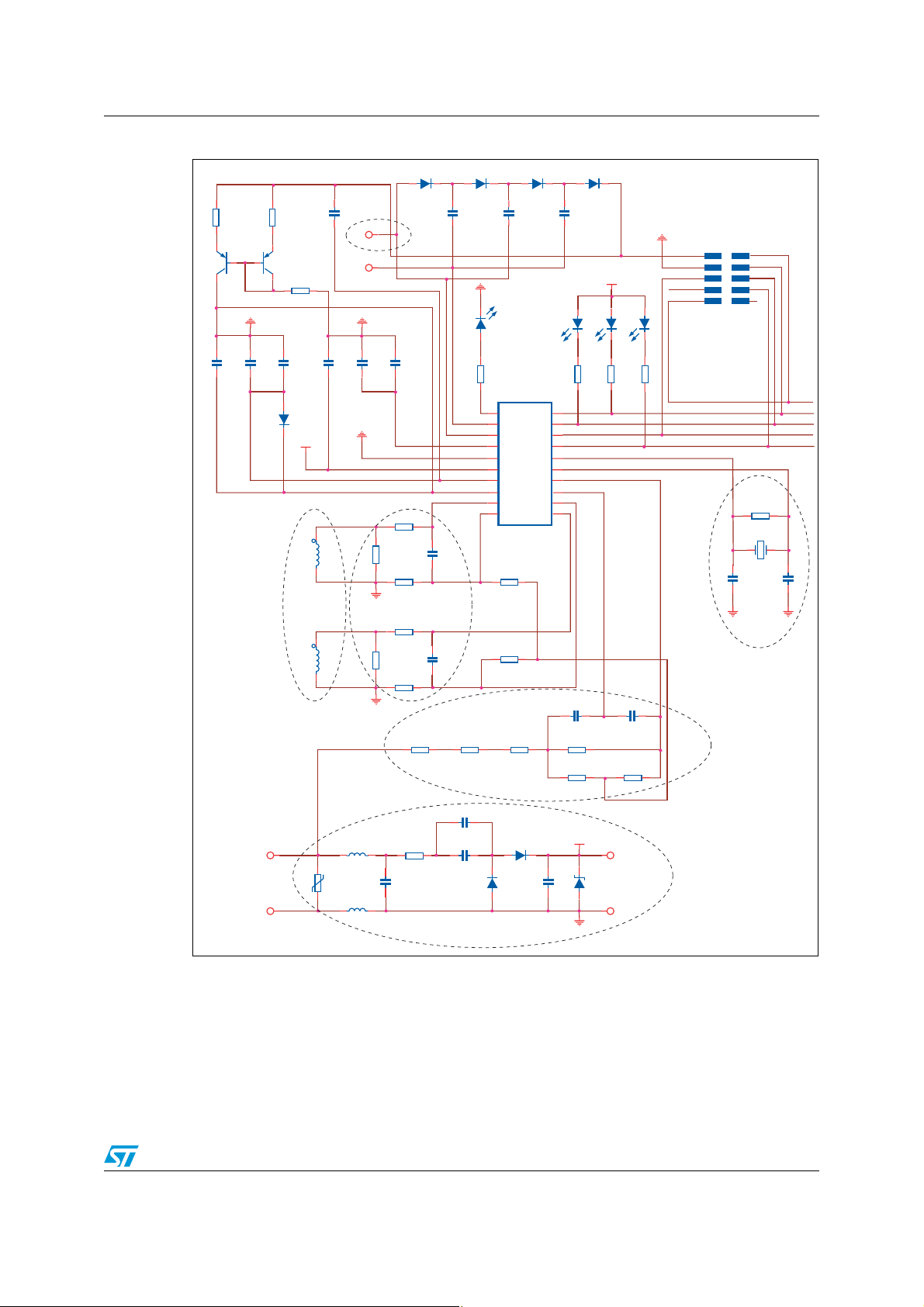
Figure 1. STPM01 External Circuit Schematics. . . . . . . . . . . . . . . . . . . . . . . . . . . . . . . . . . . . . . . . . . 5
Figure 2. Primary Current Sensing Circuit . . . . . . . . . . . . . . . . . . . . . . . . . . . . . . . . . . . . . . . . . . . . . . 6
Figure 3. Current Sense Transformer-to-Power Line Connections . . . . . . . . . . . . . . . . . . . . . . . . . . . 8
Figure 4. Shunt Module-to-Power Line Connections . . . . . . . . . . . . . . . . . . . . . . . . . . . . . . . . . . . . . 10
Figure 5. Anti-aliasing Filter. . . . . . . . . . . . . . . . . . . . . . . . . . . . . . . . . . . . . . . . . . . . . . . . . . . . . . . . 11
Figure 6. Anti-aliasing Effect . . . . . . . . . . . . . . . . . . . . . . . . . . . . . . . . . . . . . . . . . . . . . . . . . . . . . . . 11
Figure 7. Anti-aliasing Filter Magnitude Response . . . . . . . . . . . . . . . . . . . . . . . . . . . . . . . . . . . . . . 14
Figure 8. Anti-aliasing Filter Phase Response. . . . . . . . . . . . . . . . . . . . . . . . . . . . . . . . . . . . . . . . . . 14
Figure 9. Voltage Sensing Circuit . . . . . . . . . . . . . . . . . . . . . . . . . . . . . . . . . . . . . . . . . . . . . . . . . . . 15
Figure 10. Crosstalk Network. . . . . . . . . . . . . . . . . . . . . . . . . . . . . . . . . . . . . . . . . . . . . . . . . . . . . . . . 17
Figure 11. Capacitive power supply (with EMC Filter). . . . . . . . . . . . . . . . . . . . . . . . . . . . . . . . . . . . . 18
Figure 12. Capacitive Power Supply . . . . . . . . . . . . . . . . . . . . . . . . . . . . . . . . . . . . . . . . . . . . . . . . . . 19
Figure 13. Internal RC Recommended Connections . . . . . . . . . . . . . . . . . . . . . . . . . . . . . . . . . . . . . . 24
Figure 14. Quartz Recommended Connections. . . . . . . . . . . . . . . . . . . . . . . . . . . . . . . . . . . . . . . . . . 24
Figure 15. External Clock Source Recommended Connections . . . . . . . . . . . . . . . . . . . . . . . . . . . . . 25
3/27
Page 4

External Circuit Design AN2317 - Application
1 External Circuit Design
Figure 1 on page 5
shows an implementation example of the STPM01 in a simple Stepper
Counter Connector design. The main external circuits include:
● a
Current Sensing Circuit
● an
● a
● a
● a
Anti-aliasing Filter on page 11
Voltage Sensing Circuit on page 15
Capacitive Power Supply Circuit on page 18
Clock Generation on page 24
,
,
,
, and
(RC oscillator, quartz, or external clock).
4/27
Page 5
AN2317 - Application External Circuit Design
Figure 1. ST PM01 External Circuit Sc hema t ic s
D2
12121212
1
33.0R
R22
R21
2
22
Q3
3
BC8578
112
C3
C2
1.0N
1.0N
221
CURRENT SENSING
W3
VODNIK
W4
VODNIK
1
1K
2
11
Q4
BC8578
3
12
1
C16
2
R23
47K
21
C6
1MYC71MY
12
2
D1
1N4148
1
VDD
4121
TR1
12
E4622/X503
4121
TR2
12
E4622/X503
1
1
F
1
V4
510V
2
12
N
1
W6
1MY
VODNIK
1
W5
VODNIK
1
2
C5
C4
1.0N
1
R2
12
1.0k
R5
30.1R
R1
12 12
1.0k
ANTI-ALIASING FILTER
R3
12
1.0k
R6
30.1R
R4
12
1.0k
12
L6
220MYH
L3
220MYH
R24
21 21 2
82R
1
C14
1.0N
2
1
1N4148D31N4148D41N4148D51N4148
C17
2
D6
1MY
VDDA
C8
10N
10N
1
SRD 200mcd
2
1
R20
2.4K
2
20
1
2
4
5
6
8
7
9
10
1
C18
2
U1
STPM01E
LED
MON
MOP
VDD
VSS
VCC
VDDA
VOIP
IIP1
IIN1
10N
SDA
SCL
SCS
SYN
CLKOUT
CLKIN
VIN
IIN2
IIP2
1
C19
2
D7 SRD 200mcd
19
18
3
15
17
16
14
13
VIP
12
11
10N
2
1
12121
R19
2.4K
R13
2M
10N
12
2M
C11
1
2
C9
R14
4.7my
R8
261K
12
12
261K
R10
261K
R7
12
475R
R11
12
R9
150K
C20
12
220N
C1
470N
D11
21
1
DIF60
D10
DIF60
2
C15
+
VDD
121
D12
1000M
2
VDD
2
1
D8 SRD 200mcd
D9 SRD 200mcd
R18
R17
2.4K
C10
1
10N
R12
12
2.21k
W1
VODNIK
1
W2
5.6V
VODNIK
1
PI
G08 10-2V
1
3
5
VDDA
7
2
9
1
2.4K
2
12
2
1
4194.304kHz
C12
2
CRYSTAL OR RTC
OSCILLATOR
2
VOLTAGE SENSING
CAPACITIVE POWER SUPPLY
15P
2
4
6
8
10
R15
1M
Y1
1
1
C13
2
AI12296
SBG
SDA
SCL
SCS
SYN
15P
5/27
Page 6
External Circuit Design AN2317 - Application
1.1 Current Sensing Circuit
The STPM01 has two external current sensing circuits (see
1. Primar y channe l, and
2. Secondary channel.
1.1.1 Primary Current Sensing
The primary channel uses a current transformer to couple the mains current (see
The Burden resistor is used to produce a voltage between V
filter (LPF) is used to filter out the high frequency interference and has little influence on the
voltage drop between V
Figure 2. Pr imary Curr ent S ens i ng Ci rcui t
I1
IN1
I2
and V
.
IP1
Burden Resistor LPF
R2
12
1.0k
6.8R
R1
12
1.0k
R23
1R
1
R25
2
1
2
Figure 1 on page 5
IN1
and V
1
C9
2
. The Low-pass
IP1
VIN1
+
U0
10N
–
VIP1
AI12297
):
Figure 2
).
6/27
Page 7

AN2317 - Application External Circuit Design
Primary current sensing is calculated as follows:
Equation 1
N
1
------ -
I
2
⋅=
I
1
N
2
Equation 2
U
0UAI2
R23R25⋅
------- ----------- ----------- ---
⋅
+
R
23R25
N
------ --
N
1
2
I
⋅⋅==≈
1
R23R25⋅
------ ----------- ----------- ----
+
R
23R25
Assuming I
, the calculation will proceed as:
1PEAK
Equation 3
I
1PEAK
-----------------I
2PEAK
N
2000
2
=
=
------ -
------------ -
N
1
1
Equation 4
I
I
2PEAK
1PEAK
------------------ 3 m A==
2000
Equation 5
R23R25⋅
U
0PEAKUAPEAKI2PEAK
The maximum differential input voltage between V
------------------------- -
⋅ 2.6mV===
+
R
23R25
and V
IN1
is dependent on the
IP1
Programmable Gain Amplifier (PGA) selection. For the purposes of this application, use 8x
as the gain value, then U
0PEAK
= 0.15V.
Equation 6
U
APEAK
U
0PEAK
0.15V==
Equation 7
Equation 8
Equation 9
I
2PEAK
I
1PEAK
I
1RMS
R
+
23R25
2000I
I
1PEAK
------------------
------------------------- -
⋅ 172mA==
⋅
R
23R25
2PEAK
344A==
243A==
U
APEAK
2
7/27
Page 8
External Circuit Design AN2317 - Application
The primary current sensing circuit can be connected to mains as follows (see
Figure 3
):
1. The hot line voltage wire must be connected to pin F of the module.
Normally, this wire is also connected to the hot line current wire. However, during
production or to verify phases, this wire may be connected to some other line voltage
source.
2. The neutral line voltage wire must be connected to pin N of the module.
This wire is also connected to the neutral line current wire.
3. The hot line current wire must be placed through the current transformer TR1 hole
(becoming the hot load wire).
2
Use insulated 4mm
copper wire.
4. The neutral line current wire must be placed through the current transformer TR2 hole.
2
Use insulated 4mm
copper wire.
Figure 3. Current Sense Transformer-to-Power Line Connections
Neutral Line
Hot Line
FN
TR2 TR1
Neutral Load
Hot Load
W6
W5
Comp side
*
P1
AI12298
8/27
Page 9

AN2317 - Application External Circuit Design
1.1.2 Secondary current sens ing
The secondary channel uses shunt resistor structure (see
Figure 4
). The 420µW shunt
resistor is used to maximize the use of the dynamic range of the current sensing circuit.
However, there are some important conside rations when selecting a shunt structure for
energy metering applications.
● The power dissipation in the shunt must be minimized.
The maximum rated current for this design element is 20A, so the maximum power
dissipated in the shunt is calculated as follows:
2
20A()
● The higher power dissipation may make it difficult to manage the thermal issues.
420μΩ 168mW=×
Although the shunt is manufactured from manganin material, which is an alloy with a
low thermal resistance, an apparent error may occur when it reaches a high
temperature.
● The shunt should be able to resist the shortage of the phase circuit.
This reduces the shunt resistance is much as possible.
The design values used are:
– Mains voltage = 220V
RMS
,
– Ib = 2A, and
– Shunt resistance = 420µΩ.
The remaining design elements calculated from these values are as follows:
– Voltage across shunt:
2A 420μΩ 0. 00084 V=×
– Mains power dissipation:
– Error:
1.68 10
3–
× 0.44 103–× 100percent 0.0004percent=×⁄
220V 2A 0.44kW=×
9/27
Page 10

External Circuit Design AN2317 - Application
The secondary current sensing circuit can be connected to the mains as shown in
Figure 4
1. The hot line voltage wire must be connected to pin N of the module.
Normally, this wire is also connected to the hot line current wire. However, during
production or to verify phases, this wire may be connected to some other line voltage
source.
2. The neutral line voltage wire must be connected to pin F of the module.
This wire is also connected to the neutral line current wire, which passes by the
module.
3. The hot line current wire must be connected to the Shunt pole which is close to pin N of
the module.
2
Use insulated 4mm
copper wire.
4. The hot load current wire must be connected to the Shunt pole which is close to the
edge of the module.
2
Use insulated 4mm
copper wire.
Figure 4. Shunt Module-to-Power Line Connections
Neutral
Hot Line
FN
Comp side
Shunt
*
P1
Hot Load
W6
W5
LED
NLC
TPR
DIR
AI12299
:
10/27
Page 11

AN2317 - Application External Circuit Design
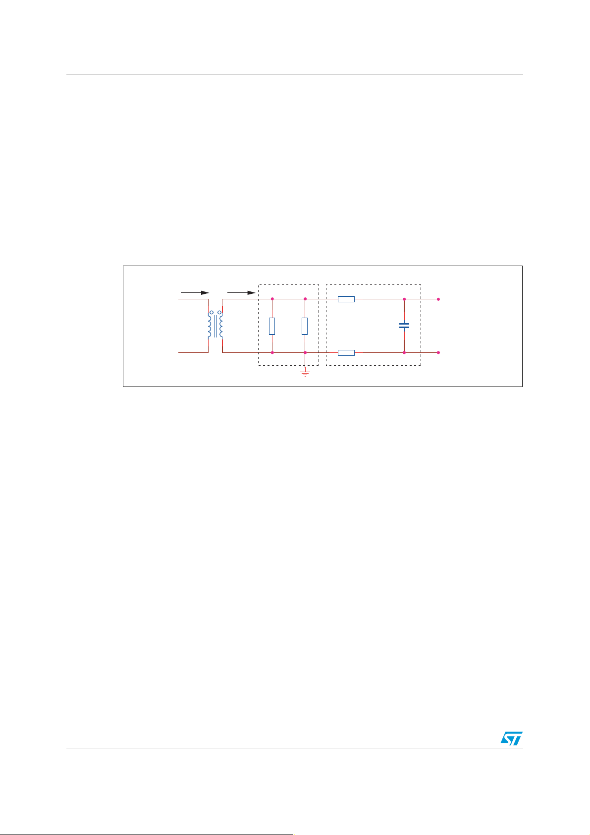
1.2 Anti-aliasing Filter
The anti-aliasing filter (
Figure 5
) is a low-pass filter. It reduces high frequency levels which
may cause distortion due to the sampling (aliasing) that occurs before the analog inputs of
an analog-to-digital converter (ADC) are introduced into the application (see
Figure 6
).
Filtering is easily implemented with a resistor-capacitor (RC) single-pole circuit which
obtains an attenuation of –20dB/dec.
Figure 5. Anti-aliasing Filter
R
U
C
U
I
R
C
O
AI12900
Figure 6. Anti-aliasing Effect
0
Image
Frequencies
2
450
Frequency - kHz
900
AI12901
11/27
Page 12

External Circuit Design AN2317 - Application
The anti-aliasing filter magnitude and phase response can be calculated as follows:
Equation 10
1
U
A
O
------- -
u
U
I
-------- jωc
------------------- 1
R
-------- -+
jωc
------------------------ -== =
1jωRC+
1
Note: The cutoff frequency is expressed as:
So
Equation 10
f
p
can be changed to:
1
--------2πτ
1
--------------- -==
2πRC
Equation 11
u
1j
f
--- -
⋅+
f
p
1
------------------- -
==
A
1
------------------- -
1j
⋅+
f
--- f
p
Equation 12
1
----------------------
A
=
u
1
+
f
⎛⎞
----
⎝⎠
f
p
2
The phase is expressed as:
Equation 13
In the module:
3
R = 2 • 10
KΩ and
C = 10nF, so then
ϕ arc–
1
--------------- - 7961.8Hz==
f
p
2πRC
f
----tan=
f
p
12/27
Page 13

AN2317 - Application External Circuit Design
According to
Equation 12
response can be seen in
● When f = 50Hz:
Equation 14
and
Equation 15
● When f = 60Hz:
Equation 16
and
Equation 17
and
Equation 13 on page 12
Figure 7
and
Figure 8 on page 14
ϕ 0.35
ϕ 0.43
, the filter’s magnitude and phase
.
°
–=
A
1≈
u
°
–=
1≈
A
u
Assume that the current lags the voltage by a phase angle, δ. After an anti-aliasing filter, a
phase error (ϕ) is introduced into the STPM01. The power factor (PF) error is calculated as:
Equation 18
δcos δϕ+()cos–
error
-----------------------------------------------
PF
δcos
100percent⋅=
When,
δ = –60° (PF = –0.5), and
f = 50Hz,
according to
Equation 14
, a phase error, ϕ = –0.35° has occurred:
Equation 19
°
–()cos–
100percent 1percent=⋅=
error
60–°()cos 60°– 0.35
----------------------------------------------------------------------------------
PF
60–°()cos
This indicates that even a small phase error will translate into a significant measurement
error at a low power factor. Thus correct phase matc hing is required in this situation.
13/27
Page 14

External Circuit Design AN2317 - Application
Figure 7. Anti-aliasing Filter Magnitude Response
0
–20
–40
Decibels (dB)
–60
1000 10000 100000 100000010010
Frequency (Hz)
Figure 8. Anti-aliasing Filter Phase Response
0
–20
–40
–60
Degrees (°)
–80
–100
1000 10000 100000 100000010010
Frequency (Hz)
AI12902
AI12903
14/27
Page 15

AN2317 - Application External Circuit Design
1.3 Voltage Sensing Circuit
The STPM01 normally uses a resistor divider as voltage input channel (see
783kΩ resistor is separated into three 261kΩ, in-series resistors (see
Figure 9
). The
Figure 1 on page 5
),
which ensure that a high voltage transient will not bypass the resistor. These three resistors
also reduce the potential across the resistors, thereby decreasing the possibility of arcing.
The following resistors are used as the resistor divider when the mains voltage is present:
● R‘ = 783KΩ, and
● R
C11 and (R
created by the circuit from migrating onto the Line or Neutral busses (see
through
=475Ω.
5
+ R15) create a filter which prevents Electromagnetic Interference (EMI)
19
Equation 24 on page 16
Equation 20
).
Figure 9. Voltage Sensin g Circui t
L2
1m
R'
783k
Z2
R'
783k
R5
475
R6
475
Z1
R19
42.2k
C11
22n
R15
100
V1
V2
AI12904
15/27
Page 16

External Circuit Design AN2317 - Application
Equation 20
Z
R
1
+()42.3KΩ==
19R15
Equation 21
Z
R5R6+()Z1⋅
------------------------------------ 930Ω==
2
++
R
5R6Z1
Equation 22
Z
2
-----2
U
1
U2–
----------------------
2R′ Z
+
V
mains
2
⎧
V
⎪
mains
=⋅==
⎨
⎪
V
mains
⎩
110 2V U10.046V=,=
220 2V U10.092V=,=
Equation 23
Z
2
----- 2
U
U1U2–
0
------------------ -
Z
-------
+
R′
2
V
mains
2
⎧
V
⎪
mains
=⋅==
⎨
⎪
V
mains
⎩
110 2V U00.092V=,=
220 2V U00.185V=,=
Z1 has little influence on the U
, thus:
0
Equation 24
R
5
-------------------
U
≈
0
R′ R5+
Note: For a specific U0, choose an appropriate combination of resistors (R5 and R’) to get that
particular U
value.
0
16/27
Page 17

AN2317 - Application External Circuit Design
1.4 Crosstalk Cancellation Network
The voltage front end handles voltages of considerable amplitude, which makes it a
potential source of noise. Disturbances are readily emitted into current measurement
circuitry where it will interfere with the actual signal to be measured. Typically, this shows as
a non-linear error at small signal amplitudes and non-unity power factors.
At unity power factor, voltage and current signals are in phase and crosstalk between
voltage and current channels merely appears as a gain error, which can be calibrated.
When voltage and current are not in phase, crosstalk will have a non-linear effect on the
measurements, which cannot be calibrated.
Crosstalk is minimized by means of good PCB planning and the proper use of filter
components in the crosstalk network. Recommended filter components are shown in
Figure 10
input. This prevents crosstalking within the STPM01. The signal subtraction is calculated in
Equation 25
Equation 25
. The network subtracts a signal proportional to the voltage input from the current
and
Equation 26
V
.
R15
R15
---------------------------- R19 R15+
V
VCI
R15
---------- R19
⋅≅⋅=
V
VCI
Equation 26
R1
V
CCI
R1
------------------------R21 R1+
V
R15
R1
---------- R21
⋅≅⋅
V
R15
---------- R21
R15
---------- R19
V
≅⋅⋅==
VCI
1.18e6–V
VCI
Note: This network must be applied to every STPM 01 design, from the voltage channel to each
current channel.
Figure 10. Crosstalk Network
+
R19
42.2k
R21
2M
R1
1k
V
CCI
Current
Channel
Input
AI12908
–
+
Voltage
Channel
–
V
VCI
Input
R15
100
17/27
Page 18

External Circuit Design AN2317 - Application
1.5 Capacitive Power Supply Circuit
The capacitive power supply circuit is shown in
● a varistor,
● the capacitive power supply , and
● the Electromagnetic Compatibility (EMC) filter.
Figure 11. Capacitive power supply (with EMC Filter)
LINE
NEUTRAL
1.5.1 Varistor
The varistor is a surge protection device that is connected directly across the AC input.
When a power surge or voltage spike exceeding a specified voltage (varistor voltage) is
sensed, the varistor's resistance rapidly decreases, creating an instant shunt path for the
overvoltage, thereby saving the sensitive control panel components. The varistor and the
line fuse are subject to damage or weakened because the shunt path creates a short circuit.
Transient
Protection
RV1
510V
Figure 10
Filter 1 Filter 2
L1
220m
C1
1n
L2
220m
Current
Limiter
82R
R1
Voltage
Divider
C2
470n
DIF60
and includes:
D1
DIF60
D2
C3
1000m
VDD
2
D3
5.1V
1
GND
AI12909
An essential point of varistor selection is t hat t he varistor can handle the peak pulse current,
which is 110% of the maximum current at which the varistor voltage does not change. If the
peak pulse current rating is insufficient, then the varistor may be damaged. The main
voltage is 220V
, and sometimes the maximum will r eac h 265V
RMS
K10*300V varistor is chosen for this application.
18/27
.Thus, an MOKS
RMS
Page 19

AN2317 - Application External Circuit Design
1.5.2 Capacitive Power Supply
There are several ways to convert AC voltage into the DC voltage required by STPM01.
Traditionally, this is done with a transformer and rectifier circuit. There is also switching
power supply solution. However , these two solutions are expensive and take up a
considerable amount of PCB space.
To provide a low-cost, alternative solution, a transformerless power supply can be used (see
Figure 12
Figure 12. Capacitive Power Supply
).
LINE
UIN
R1
82R
C2
470n
IIN
D2
DIF60
D1
DIF60
C3
1000m
VDD
2
D3
5.1V
1
NEUTRAL
GND
AI12914
19/27
Page 20

External Circuit Design AN2317 - Application
The input current (IIN) is limited by R1 and the capacitive reactance of C2 (see
and
Equation 29
), and is expressed as:
Equation 27
V
I
IN
IN R MS()
------------------------ -=
X
+
C2R1
where,
X
= C2 reactance.
C2
Note: R1 is used to limit inrush current, but it dissipates power.
By adding a low-cost half-wave rectifier, current is allowed to be supplied by the source
during the positive half, where,
● V
= RMS voltage of the half-wave AC wav eform, and is expressed as follows:
INRMS
Equation 28
V
1
PEAKVZ
-- -
V
IN RMS()
------------------------------ -
⋅=
2
2
where,
= mains peak voltage (i.e. United States = 115V/60Hz and
V
PEAK
Europe = 220V /50Hz ), and
= the voltage drop across D1 and D3.
V
Z
● X
= Capacitor reactance, and is expressed as:
C2
Equation 28
–
Equation 29
1
----------------=
2πfC
2
with those in
Equation 28
and
Equation
By substituting the values expressed in
29
, the results are as follows:
X
C2
Equation 27
Equation 30
I
----------------------------------------
IN
22X
V
PEAKVZ
C2R1
–
+()
2V
----------------------------------------==
22X
–
mainsVZ
+()
C2R1
Assuming that the voltage drop across each diode is 0.7V, then the total voltage drop is
expressed as:
Equation 31
V
Z
V
D1VD3
5 0.7 2 6.4V=⋅+=+=
20/27
Page 21

AN2317 - Application External Circuit Design
When these application parameters are considered:
= 220VAC,
V
mains
f = 50Hz, and
= 6.4V (see
V
Z
Equation 31
), the calculated IIN would be:
Equation 32
I
15.7mA=
IN
Selecting components in the circuit is a critical consideration. As a general rule, components
should be sized at twice the maximum power calculated for each device.
For example, by using the I
value in
IN
Equation 32
and VDD = 5V to choose an appropriate
Zener diode, the results required to make the selection are expressed as follows:
Equation 33
2
V
DDIIN
R10.02W=⋅=
and
Equation 34
P
D3
VD3I
IN
5.1 0.0157 0.08W=⋅=⋅=
Thus, a ZMM SOD 80*5.1V G Zener Diode is used.
21/27
Page 22

External Circuit Design AN2317 - Application
1.5.3 EMC Filter
EMC has become an important power supply parameter. In order to deal with common and
differential mode noise, a two-part AC filter is added (see
● Differential filter (Filter 1)
Inductors L
, and C1 represent a differential filter for DM (differential mode) noise
1/L2
trying to enter the power supply. DM noise is produced by current flowing along either
the Line or Neutral conductor, and returning by the respective other. This produces a
noise voltage between the Line and Neutral conductors.
The filter will be designed for at least 10 times the line frequency, thereby resulting in a
frequency of 600Hz. The indication is then, that the cutoff frequency (f
below 600Hz.
Capacitor C
is X Class capacitor, used to reduce differential noise. To ensure that C1
1
does not fail because of the surge or short circuit current, it must be able to withstand
twice the mains voltage value. Keeping this requirement in mind, f
follows:
Equation 35
f
C
---------------------------------------------- -7.59Hz=≈
2π L
1
+()C1⋅
1L2
Figure 11 on page 18
) must not be
C
is calculated as
C
).
Note: Generally, a specific fC value is chosen, then the inductors are tuned to that value.
22/27
Page 23

AN2317 - Application External Circuit Design
● Capacitor filter (C
Capacitor C
requirements expressed in
, Filter 2)
3
is used as a filter. Considering load RL, the size of C3 must satisfy the
3
Equation 36
:
Equation 36
RLC1525∼()T=
In fact, considering that the charge stored in the capacitor is:
Equation 37
TQ=
I
L
where,
I
= the load current, and
L
T = the AC sine wave period, and
the output ripple voltage is expressed as:
Equation 38
Q
ΔV
----=
C
then the capacitor C value can be calculated by using a fixed voltage ripple value:
Equation 39
I
T
L
ΔV
--------=
C
then, fixing our ripple to ΔV=200mV we can calculate C value accordingly.
For the purposes of this application, C is calculated as follows:
Equation 40
10mA
-------------------------------------- 1000μF==
C
200m V 50Hz
The STPM01 power supply (V
CC
seems to be enough to change the D3 diode (see
⋅
) configuration range is from 3.3V to 6V. While it
Equation 34
selected ZMM SOD 80*5.1V G Zener Diode, if the output current is too high, then the
C
value must be reduced.
2
Note: Usually it is not necessary to use resistor R1 in the circuit.
) from the previously
23/27
Page 24

External Circuit Design AN2317 - Application
1.6 Clock Generation
All of the STPM01 internal timing is based on the CLKOUT oscillation signal. This signal can
be generated in three different ways:
● RC (see
This oscillator mode can be selected using the RC configuration bit. If RC = 1, then the
STPM01 will r un usi ng the RC os cillat or. A resistor connected between CLKIN and
Ground will set the RC current.
Note: For 4MHz operation, the suggested settling resistor is 12k.
● Quartz (see
The oscillator will work with an external crystal.
Figure 13. Internal RC Recommended Connections
Figure 13
Figure 14
)
)
V
CLKINCLK
SS
OUT
12k
Figure 14. Quartz Recommended Connections
V
CLKINCLK
SS
1M
4194MHz
AI12915
OUT
15pF15pF
AI12916
24/27
Page 25

AN2317 - Application External Circuit Design
● External Clock (see
Figure 15
)
The clock generator is powered from analog supply, and is responsible for two tasks:
a) to retard the turning on of some of the function blocks after Po wer-on Reset (POR)
in order to help smooth start the external power supply circuitry and keep all major
loads off of the circuit, and
b) to provide all necessary clocks for the analog and digital parts. Two nominal
frequency ranges are expected,(1) from 4.000MHz to 4.194MHz, or (2) from
8.000MHz to 8.192MHz.
Figure 15. External Clock Source Recommended Connections
V
CLKINCLK
SS
OUT
–
AI12917
25/27
Page 26

Revision History AN2317 - Application
2 Revision History
Table 1. Document revision history
Date Revision Changes
14-Apr-2006 1 Initial release.
26/27
Page 27

AN2317 - Application
y
y
Please Read Caref u ll y:
Information in this document is provided solely in connection with ST products. STMicroelectronics NV and its subsidiaries (“ST”) reserve the
right to make changes, corrections, modifications or improvements, to this document, and the products and services described herein at an
time, with out notice.
All ST products are sold pursuant t o ST’s terms and conditio ns of sale.
Purchase rs are solely responsible f or the ch oi ce, selec tion and us e of the ST products and services des cribed he rei n, and S T assumes no
liability whatsoever relating to the choice, selection or use of the ST products and services described herein.
No license, express or implied, by estoppel or otherwise, to any intellectual property rights is granted under this document. If any part of this
document refers to any third party produ ct s or servic es it shall n ot be deeme d a license grant by ST for the use of such thir d party pro ducts
or services , or any intel lec tual pro per ty cont aine d ther ein or con sidere d as a warra nty c overi ng th e use i n any mann er w hats oever of such
third party products or services or any intellec tual prope rt y contained t herein.
UNLESS OTHERWISE SET FORTH IN ST’S TERMS AND CONDITIONS OF SALE ST DISCLAIMS ANY EXPRESS OR IMPLIED
WARRANTY WITH RESPECT TO THE USE AND/OR SALE OF ST PRODUCTS INCLUDING WITHOUT LIMITATION IMPLIED
WARRANTIES OF MERCHANTABILITY, FITNESS FOR A PARTICULAR PURPOSE (AND THEIR EQUIVALENTS UNDER THE LAWS
OF ANY JURISDICTION), OR INFRINGEMENT OF ANY PATENT, COPYRIGHT OR OTHER INTELLECTUAL PROPERTY RIGHT.
UNLESS EXPRESSLY APPRO VED IN W RITING B Y AN AUTHORIZE REPRESE NTATIVE O F ST, ST PRODU CTS ARE N OT DESI GNED,
AUTHOR I Z ED OR WARRANTED F OR USE IN MILITARY, AIR CRAFT, SPACE, LIFE SAVING, OR L IF E SUSTAINING APP L ICATIONS,
NOR IN PRODUCTS OR SYSTEMS, WHERE FAILURE OR MALFUNCTION MAY RESULT IN PERSONAL INJURY, DEATH, OR
SEVERE PROPERTY O R ENVIRONMENTAL DAMAGE.
Resale of ST products with provisions different from the statements and/or technical features set forth in this document shall immediately void
any warran ty gr anted by ST fo r the ST produc t or se rvice d es cribed he rein and shall not c reat e o r extend in a ny mann er wha tsoe ver, an
liability of ST.
ST and the ST logo are trademarks or registered trademarks of ST in various c ountries.
Information in this do cument super sedes and replaces all inf ormation pr eviously supplied.
The ST logo is a registered trademark of STMicroelectronics. All other names are the property of their respective owners.
© 2006 STMi croelectronics - All ri ghts reserved
STMicroelectron ics group of co m panies
Austra l i a - Be l gi um - Brazil - Canada - Chi na - Czech Republic - Finl and - Franc e - Germany - Ho ng Kong - India - Israel - It al y - Japan -
Malaysi a - M al ta - Morocco - Singapore - Spain - Sweden - Swit zerland - Un i ted Kingdom - Uni ted States of America
www.st.com
27/27
 Loading...