

Page 1
AN2316
Application Note
Improved ST7LITE05 AC Chopper Driver Solution
Introduction
This application note presents an AC motor or load circuital solution improvement of
efficiency over the one discussed in a previously published application note, AN1255.
Above all, this solution does not have limits on where it may be applied, embracing all types
of AC asynchronous monophase motor applications (e.g. refrigerators, hydraulic pumps,
fans, and lamps).
Due to the increasing electric pollution of the environment, European standards impose
restrictions on Electromagnetic Compatibility (EMC). The proliferation of non-linear loads
and the consequential increase in harmonics pollution in power distribution lines have
induced various technical committees to establish maximum limits on the harmonic content
produced by all industrial and domestic devices. Manufacturers of these devices are
required to conform to this new standard and develop products which function with new
operational characteristics.
The most common method used to vary the AC monophase motor voltage is a TRIACbased phase angle partialization technique. Although this is a simple, low-cost solution that
has been used for several years, it is problematic because of the excessive harmonic
distortion which reduces the efficiency of the entire system. These systems typically include
a complex inverter drive which is quite expensive, and, while they can solve the load’s
harmonic content problems, they do not address those same problems in the electric lines.
March 2006 Rev 1 1/24
www.st.com
Page 2

Contents AN2316 - Application Note
Contents
1 STEVAL-IHM006V1 Circuit Description . . . . . . . . . . . . . . . . . . . . . . . . . . 4
2 EMC Precompliance Measurement . . . . . . . . . . . . . . . . . . . . . . . . . . . . 10
2.1 Electrical Conditions . . . . . . . . . . . . . . . . . . . . . . . . . . . . . . . . . . . . . . . . . 11
2.2 EM C D ouble-Filter Bill of Mater ials . . . . . . . . . . . . . . . . . . . . . . . . . . . . . 11
3 Safety and Operating Instructions . . . . . . . . . . . . . . . . . . . . . . . . . . . . . 13
3.1 STEVAL-IHM006V1 Board Installation . . . . . . . . . . . . . . . . . . . . . . . . . . . 13
3.2 Environmental Considerations . . . . . . . . . . . . . . . . . . . . . . . . . . . . . . . . . 14
3.3 Mandatory Checks Before Operation . . . . . . . . . . . . . . . . . . . . . . . . . . . . 14
3.4 Start-up Procedure . . . . . . . . . . . . . . . . . . . . . . . . . . . . . . . . . . . . . . . . . . 15
4 ST7FLITE05 Software Description . . . . . . . . . . . . . . . . . . . . . . . . . . . . . 16
4.1 Peripheral Initialization . . . . . . . . . . . . . . . . . . . . . . . . . . . . . . . . . . . . . . . 17
4.2 Firmware Configuration . . . . . . . . . . . . . . . . . . . . . . . . . . . . . . . . . . . . . . 18
4.3 Development Tools . . . . . . . . . . . . . . . . . . . . . . . . . . . . . . . . . . . . . . . . . . 19
5 Library Source Cod e . . . . . . . . . . . . . . . . . . . . . . . . . . . . . . . . . . . . . . . . 22
5.1 Software downloa ds . . . . . . . . . . . . . . . . . . . . . . . . . . . . . . . . . . . . . . . . . 22
5.2 File Structure . . . . . . . . . . . . . . . . . . . . . . . . . . . . . . . . . . . . . . . . . . . . . . 22
6 Revision history . . . . . . . . . . . . . . . . . . . . . . . . . . . . . . . . . . . . . . . . . . . 23
2/24
Page 3

AN2316 - Application Note List of Figures
List of Figures
Figure 1. Two-Switch Drive Motor Schematic (ST patented). . . . . . . . . . . . . . . . . . . . . . . . . . . . . . . . 6
Figure 2. Basic Working Principal Illustration. . . . . . . . . . . . . . . . . . . . . . . . . . . . . . . . . . . . . . . . . . . . 8
Figure 3. System Waveforms. . . . . . . . . . . . . . . . . . . . . . . . . . . . . . . . . . . . . . . . . . . . . . . . . . . . . . . . 9
Figure 4. EMC Measure ment Schematic. . . . . . . . . . . . . . . . . . . . . . . . . . . . . . . . . . . . . . . . . . . . . . 10
Figure 5. EM C Double -Filter Stage Schem atic . . . . . . . . . . . . . . . . . . . . . . . . . . . . . . . . . . . . . . . . . 11
Figu r e 6 . 20kH z Switc h in g F r e quen c y EMC An a lysi s . . . . . . . . . . . . . . . . . . . . . . . . . . . . . . . . . . . . 12
Figu r e 7 . 35kH z Switc h in g F r e quen c y EMC An a lysi s . . . . . . . . . . . . . . . . . . . . . . . . . . . . . . . . . . . . 12
Figure 8. STEVAL-IHM0 06V1 Board Layout . . . . . . . . . . . . . . . . . . . . . . . . . . . . . . . . . . . . . . . . . . . 15
Figure 9. ST7FLITE05 Flow Diagram . . . . . . . . . . . . . . . . . . . . . . . . . . . . . . . . . . . . . . . . . . . . . . . . 16
Figure 10. Softec STVD7 v3.10 . . . . . . . . . . . . . . . . . . . . . . . . . . . . . . . . . . . . . . . . . . . . . . . . . . . . . . 19
Figure 11. ST7 Visual Programm er . . . . . . . . . . . . . . . . . . . . . . . . . . . . . . . . . . . . . . . . . . . . . . . . . . . 21
3/24
Page 4

STEVAL-IHM006V1 Circuit Description AN2316 - Application Note
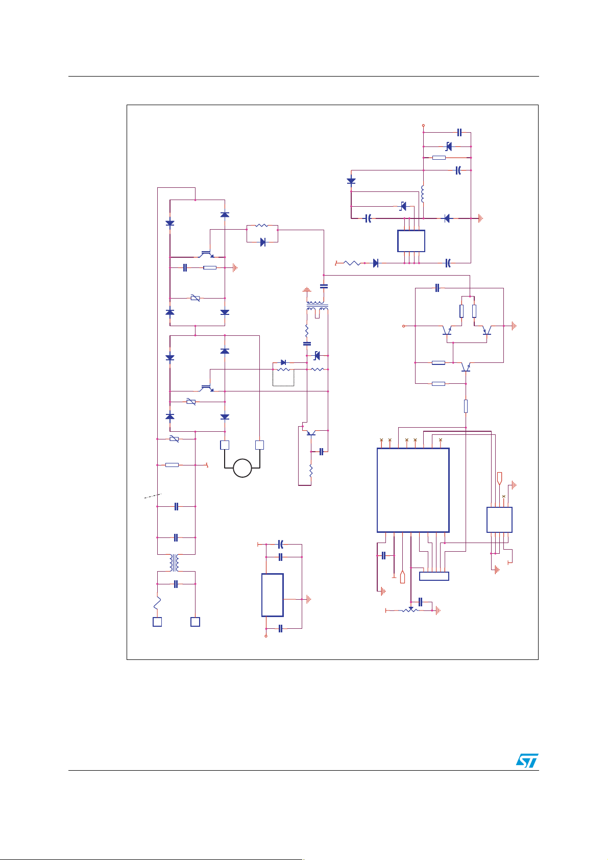
1 STEVAL-IHM006 V1 Circuit Description
This ST-patented solution uses a working switch mode to solve third harmonic problems.
The base circuit can be viewed as a mains vol tage double-chopper without any preliminar y
AC/DC conversion type (see
Note: The AC chopper STEVAL-IHM006V 1 provides customers with a demo that regulates the
voltage in AC motors or loads of up to 300W. This allows the user to demonstrate smooth,
silent, and efficient regulation with respect to TRIAC solutions.
The double-chopper is a device which energizes the load beginning from any level of the
sinusoidal voltage wave and demagne tizes the load with a freewheeling current system,
thereby obtaining voltage and current regulation of the load.
Starting from a perfect sinusoidal-shaped mains curve, the regulated current is also
sinusoidal for all the power levels that the user desires to transfer to the load. By neglecting
the electronic device losses, the circuit incoming power S is equa l to the outgoing power:
Equation 1
SV
Figure 1 on page 6
AC RMS()IAC RMS()
⋅
=
V
).
⋅=
LOAD RMS()
I
LOAD RMS()
where,
V
AC(RMS)
I
AC(RMS)
V
LOAD(RMS)
I
LOAD(RMS)
The I
= Root Mean Squared (RMS) Mains Volt age,
= RMS Input Current,
= RMS Load Voltage, and
= RMS Output Current.
AC(RMS)
and I
LOAD(RMS)
currents are related as follows:
Equation 2
I
LOAD RMS()
------ ----------- ----------- ---------- -
I
AC RMS()
V
AC RMS()
=
------ ------------ ----------- ----------- --
V
LOAD RMS()
The circuit operates as a converter, particularly as an AC/AC converter or transformer. It has
no limitation in terms of load impedance since it works with both, inductive and ohmic loads,
with notable angles between the current and the vol tag e.
4/24
Page 5

AN2316 - Application Note STEVAL-IHM006V1 Circuit Description
The circuit is based on the fo llowing parts (see
● IGBT Z1
Figure 1
):
Together with diodes D1, D2, D5, and D6, it performs current freewheeling (only for
inductive load).
● IGBT Z2
Together with diodes D3, D4, D7, and D8, it is the main switch through which the load is
energized.
● Pulse Transformer T1
It allows the signal derived from the PWM generator to be transferred to the Z1 gate.
This component electrically insulates the input from the output’s entry signal and phase
inversion.
● PWM generator
This is provided by the ST7Lite05 microcontroller.
5/24
Page 6
STEVAL-IHM006V1 Circuit Description AN2316 - Application Note
Figure 1. Two-Switch Dri ve Mo t or S che m at i c (S T patented )
+15V
C15
0.1µF
D15
18V
R10
12K 1/4W
D11
STTH108
D13
15V
R7
NTC22
12
CONTROL
V
+
C10
10µF 25V
t°
D12
STTH108
U3
123
+15V
45
S
S
FB
VDD
DDD
D
678
D4
D8
STTH306
R3
470-1/4W
STTH306
1
Z2
STGP7NB60HD
2
3
R2
C2
3.3nF
5.6-1/4W
D3
D2
250V10L
STTH306
RV3
D7
D6
STTH306
1
Z1
STGP7NB60HD
2
3
STTH306
STTH306
D9
1N4148
NOT ASSEMBLED
pulse transformer
C3
0.1µF-100V
D16 1N4148
R15
1.2k
C4
0.1µF-100V
T1
17
294
5
0
R4
D10
18V
R5
270K
PHASE
RS-196-375
L1 1mH
D14
STTH108
VIPer12A DIP
+
C12
0.1µF
Q1
BC547
R9
2.2K
R8
470K
+
C14
C13
1µF-450V
R11 15
Q2
10µF 25V
R13 0
BC547
Q3
BC557
S 1
1
Line filter
F1
1
J1
D1
R1
4
T2
3
5 A
STTH306
250V14L
220K 1/2W
C1
C17
1
2
C16
MAINS
320VAC
RV2
250V10L
RV1
1µF 250VAC
100nF x 2
phase
100nF x 2
1
J2
PHASE
D5
J3
PHASE
STTH306
1
M
AC
ASYNCHRONOUS
1
J4
MOTOR
+5V
1
OUT
IN
U1
L78L05A/TO92
3
+15V
NOT ASSEMBLED
C5
47µF-25V
+
C7
0.1µF
GND
2
C6
0.1µF
BC557
321
Q5
C18
100pF
R14 R
NOT ASSEMBLED
NOT ASSEMBLED
16151413121110
PA1
PA3
PA4
PA0/LTIC
PA2/ATPWM0
VSS
VDD
RESET
U4
SS/AIN0/PB0
1234567
AIN0
C25
100nF
+5V
RESET
+5V
R6
22K
9
PA7
PA5/ICCDATA
PA6/MCO/ICCCLK
MISO/AIN2/PB2
MOSI/AIN3/PB3
SCK/AIN1/PB1
8
1
C8
0.1µF
R12 10K
CLKIN/AIN4/PB4
ST7LITE09
65432
J10
CON6_0
246
13579
JP1
AI12268
RESET
8
10
+5V
CON10A
6/24
Page 7

AN2316 - Application Note STEVAL-IHM006V1 Circuit Description
In order to avoid short-circuiting the mains through switches Z1 and Z2, they must work in a
complementary manner. When Z1 is ON, Z2 must be OFF and vice-versa.
For example, if the line vol tage at J1 i s posi tiv e wi th respect to J2, and the PWM signal goes
from high-to-low, Z2 switches ON with a delay inserted by its own gate capacitance and by
resistor R3 so the load is energized. In the meantime, Z1 swit ches OFF instant aneously.
Note: In this condition, if the current is positive (i.e. it goes into J1 and comes out from J2), it will
flow through D4, Z2, D7, and the load. Conversely, if the current is negative, it will be going
out from J1 and closing through the load, D3, Z2, and D8.
As is the case with the current, when the PWM goes from low-to-high, Z2 is turned OFF
instantaneously , while Z1 is switched ON with a delay. This enables a freewheeling current
to flow through Z1.
Given these relationships, if “δ” is the duty cycle (see
is may be expressed as:
Equation 3
V
t() δ VACt()⋅δV
LOAD
where,
= Load voltage,
V
LOAD
= Mains voltage, and
V
AC
= Maximum sinusoida l vo l t age.
V
MAX
The load current may be expressed as:
Equation 4
I
LOAD
t()
1
-- -
δ
IAC⋅ t()
1
-- -
I
MAX
δ
where,
I
= Load current,
LOAD
= Input current,
I
AC
= Maximum current value, and
I
MAX
ϕ = the angle between the current and voltage.
Figure 2 on page 8
MAX
ωt()sin⋅⋅==
ωt ϕ+()sin⋅⋅==
), the load voltage
7/24
Page 8
STEVAL-IHM006V1 Circuit Description AN2316 - Application Note
The relationships expressed in
Equation 3
and
Equation 4
, and
Figure 2
show that it is
possible to control power fed to the load by changing the PWM signal duty cycle.
Note: The load is assumed to be inductive so the high frequency harmonics are filtered in the
current waveform (see Figure 3 on page 9 for system wavefor m deta ils).
Figure 2. Basic Working Principal Illustration
Bi-directional PWM Chopping
V
line
Load Current
t
duty cycle
Duty Cycle Increase
t
AI12267
8/24
Page 9

AN2316 - Application Note STEVAL-IHM006V1 Circuit Description
Figure 3. System Waveforms
VAC, I
LOAD
V
CONTROL
V
G1
VAC
I
LOAD
t
a
t
b
tON
tOFF
V
G2
tS
Current in
point i1
Current in
Z1 switch
Legend:
a = line voltage and load cur rent
b = PWM control signal generated by the ST7Lite05 microcontroller
c, d = Z1 and Z2 gate signals
e = section S1 current (see
Figure 1 on page 6
)
c
t
t
d
t
e
t
f
AI12269
f = current through switch Z2
9/24
Page 10

EMC Precompliance Measurement AN2316 - Application Note
2 EMC Precompliance Measurement
Electromagnetic Compatibility (EMC) measurement requires us e of the Line Impedance
Stabilization Network (LISN).The LISN operates as a filter between the line and test board,
providing clean energy to the syst em under test. It collects al l the emissions coming from the
systems under test (>9kHz) and sends the noise to the EMC analyzer (see
Figure 4. EMC Measurement Schematic
AC-Chopper Board
Load
Figure 4
).
Insulation
Transformer
LISN
EMC Analyzer
AI12289
Caution: For safety reasons, an insulated 1:1 transformer is used to avoid a possible ground current
loop.
Table 1. AC Chopper EMC Limits
Description
(1)
Limit Line Frequency Range
EN55014 Conducted <700W, Motors, Quasi-pe ak 150kHz to 30MHz
EN55014 Conducted <700W, Motors, Average 150kHz to 30MHz
1. EMC AC chopper measurem ent at 20kHz switching frequency (CISPR-14), per EN55014 standard.
2. Instrument used: E7400 Agilent Technology
(2)
10/24
Page 11
AN2316 - Application Note EMC Precompliance Measurement
2.1 Electrical Conditions
● V
●
● Motor voltage = 230V
●
= 230V
INPUT
AC
Motor type = Asynchronous with capacitor
AC
Motor current =1.5A
The on-board EMC filter is not optimized for every kind of load, so users need to consider
that the included filter might be inadequate for certain applications.
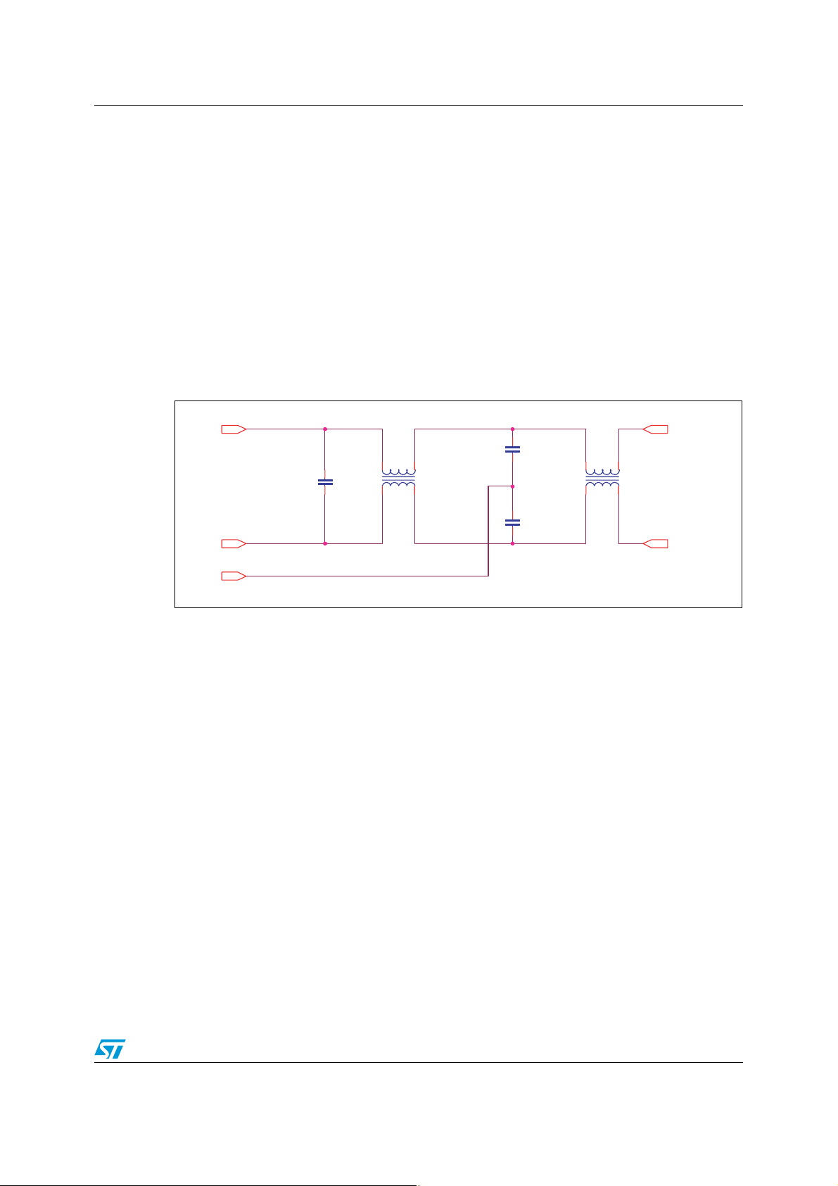
A double-filter stage ( see
Figure 5
) is required to obtain good EMC results (acceptable EMC
level) without the included filter (T2, C16, and C17), use the recommended filter mentioned
in
Figure 5
. The measured results are shown in
Figure 6
and
Figure 7 on page 12
.
Note: In order for the f ilter to be effective, the motor case must be connected to the earth-ground.
Figure 5. EMC Double-Filter Stage Schematic
Mains
Mains
0.47µF 230VAC
Common mode filter 10mH
X2
C1
2.2nF 400VAC
T1
5
1
8
4
2.2nF 400VAC
Y2
Y2
Common mode filter 111µH
C2
5
1
C3
P
T2
8
To the AC-Chopper
4
Circuit
N
EARTH GROUND
2.2 EMC Double-Filter Bill of Materials
C1 = 0.47µF 230VAC X2
C2 = C3 = 2.2nF 230V
T1 = 10mH common mode filter (to be designed in terms of current, depending on the final
load to be driven). For this application, the type used is TDK 103Y1R2X3X.
T2 = 111µH common mode filter (to be designed in terms of current, depending on the final
load to be driven).
AC
Y2
AI12290
11/24
Page 12

EMC Precompliance Measurement AN2316 - Application Note
Figure 6. 20kHz Switching Frequency EMC Analysis
Mkr1 15.08MHz
21.44dBµV
1
Ref 75dBµV
Peak
Log
10
dB/
W1 S2
S3 FC
AA
#Atten 10dB
Start 150kHz
Res BW 9kHz
VBW 30kHz
Figure 7. 35kHz Switching Frequency EMC Analysis
Ref 75dBµV #Atten 10dB
Peak
Log
10
dB/
W1 S2
S3 FC
AA
Start 150kHz
Res BW 9kHz VBW 30kHz
Sweep 881.3ms (1515pts)
Stop 30MHz
AI12291
Mkr1 15.08MHz
25.42dBµV
1
Stop 30MHz
Sweep 881.3ms (1515pts)
AI12292
12/24
Page 13

AN2316 - Application Note Safety and Operating Instructions
3 Safety and Operating Instructions
Note: Please read this section before attempting any operation with this manual.
The AC chopper board is designed for demonstration purpos es only, and shall not be used
for electrical installation or machinery. The technical data, as well as information concerning
the power supply conditions shall be taken from the documentation and strictly observed.
The AC chopper driver poses several inherent hazards dur ing installation and operation,
including bare wires and hot surfaces. All operations involving transportation, installation
and use, as well as maintenance are to be carried out by skilled technical personnel
(national accident prevention rules must be observed). For the purposes of these basic
safety instructions, “skilled technical personnel” are defined as suitably qualified people who
are familiar with the installa ti o n, use , and maint e nance of po we r electro n i c syste m s.
Danger: There is danger of serious personal injury and damage to
property, if the Kit or its components are improperly used or
installed incorrectly.
3.1 STEVAL-IHM006V1 Board Installation
The installation and cooling of the demo board shall be in accordance with the specifications
and the targeted application.
● The motor drive converters shall be protected against excessive strain. In particular, no
components are to be bent, or isolating distances altered during the course of
transportation or handling.
● No physical contact shall be made with electronic components and contacts.
● The boards contain electrostatically sensitive components that are prone to damage
through improper use. Electrical components must not be mechanically damaged or
destroyed (to avoid potential health risks).
Warning: Applicable national accident prevention rules must be
followed when working on the main power supply with a
motor or AC load.
Note: Do NOT expose the kit to ambient temperatures of over 35°C, as this may harm the
components or reduce their lifetimes.
13/24
Page 14

Safety and Operating Instructions AN2316 - Application Note
3.2 Environmental Considerations
The STEVAL-I HM0 06V 1 AC chopper demo board must only be used in a power laboratory.
The high voltage used in any AC drive system presents a se rious shock hazard. A complete
laboratory setup consists of:
● an isolated AC power supply,
● the STEVAL-IHM 006V1 demo board,
● an AC Induction motor, and
● an isolated (laboratory) power supply for +15V (as needed).
The Kit is not electrically isolated from the AC input. The microprocessor is grounded
without insulation with respect to the mains so that it and the associated circuitry are hot.
They MUST therefore be isolated from user controls and serial interfaces.
Note: Any measurement equipment must be isolated from the main power supply before powering
up the motor drive. To use an oscilloscope with the Kit, it is safer to isolate the AC supply
AND the oscilloscope. This prevent s a shock occurring as a result of touching any SINGLE
point in the circuit, but does NOT prevent shocks when touching TWO or MORE points in
the circuit.
An isolated AC power supply can be constructed using an isolation transformer and a
variable transformer. A schematic of this AC power supply may be found in the Application
Note, “AN438, TRIAC + M icroc ontrolle r: Safety Precautions for Development Tools”.
(Although this Application Note was written for TRIACs, the isolation constraints still apply
for fast -switching semiconductor devices such as IGBTs).
Note: Isolating the application rather than the oscilloscope is highly recommended in any case.
3.3 Mandatory Checks Before Operation
The following ver ificat ions must be performed before operating the demo board:
● The motor load is connected and earth-grounded,
● there is no metal part on, below , or around the PC boards, and there are no unintended
earth/ground loops caused by peripheral (e.g. test) equipment (e.g. PC or
oscilloscope), and
● the motor and mechanical load are safely housed so that rotating parts cannot be
inadvertently accessed and cause injury (e.g., loose clothing, long hair).
Warning: The high voltage levels used to operate the motor drive could
present a serious electrical shock hazard. This demo board
must be used only in a power laboratory only by engineers
and technicians who are experienced in power electronics
technology.
14/24
Page 15

AN2316 - Application Note Safety and Operating Instructions
3.4 Start-up Procedure
1. Connect the AC m otor or AC load on the board to connectors J3 and J4 (see
Sequencing is arbitrary.
2. Connect the current probe on one motor line in order to monitor motor current on the
oscilloscope.
3. Apply the heat sink spreader (not included in the STEVAL-IHM006V1) on the two
IGBTs using the appropriate insulation foil.
4. Set the potentiometer R6 in arbitrary position. This changes the main switch Z2 duty
cycle.
5. Apply the main voltage supply to connectors 230V
6. Rotate potentiometer P2 Clockwise (CW) to begin increasing the motor load voltage.
The resulting current wavefor m should remain fairly sinusoidal.
Warning: The entire circuit board and motor output terminals are
always “hot” with respect to earth ground, even when the
drive is in a stopped condition.
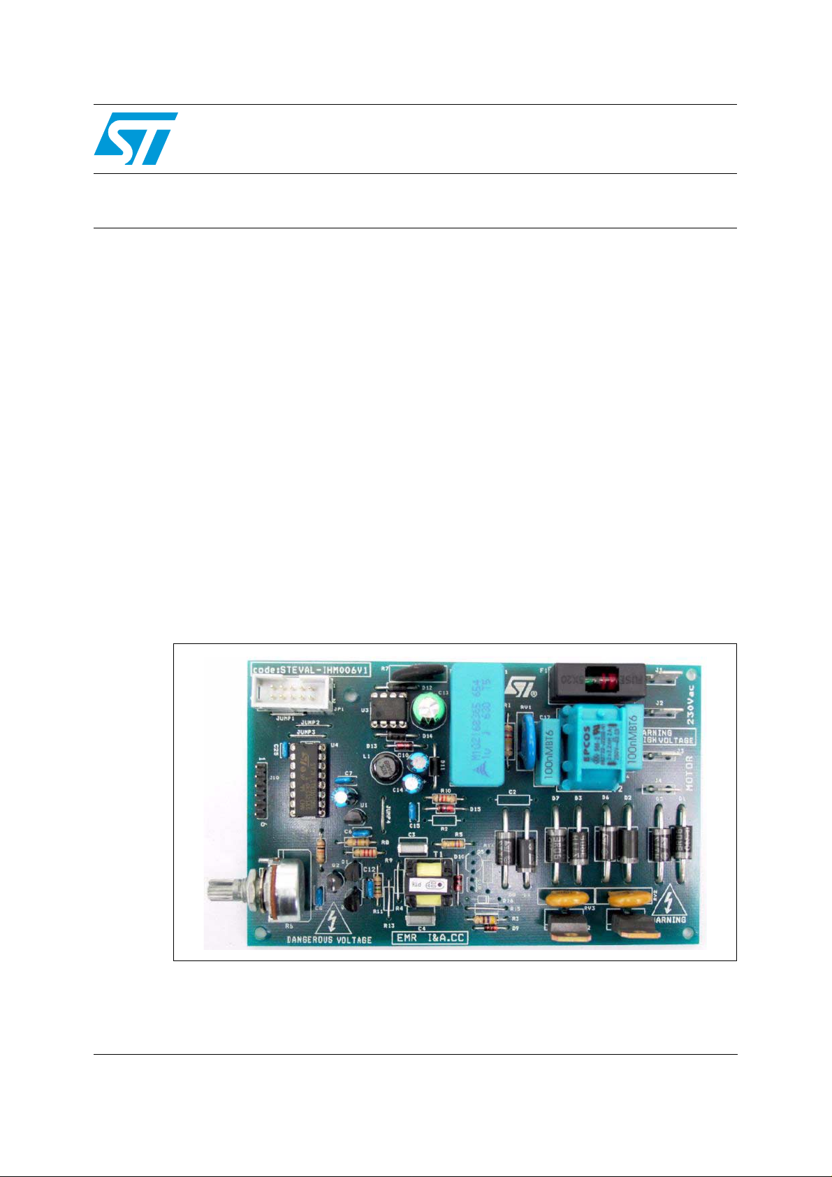
Figure 8. STEVAL-IHM006V1 Boa rd Layout
J1 and J2.
AC
Figure 8
).
15/24
Page 16

ST7FLITE05 Software Description AN2316 - Application Note
4 ST7FLITE05 Software Description
The ST7FLITE05 firmware allows designers to generate the PWM signal required to drive
the STEVAL-IHM006V1 AC chopper Z1 and Z2 IGBTs (see
the Softec STVD7 Toolset v3.10 and 16K limited free version of Cosmic Compiler v4.5c.
The system may be customized by setting parameters in the “Param.h” header file,
including:
● switching frequencies,
● maximum and minimum applicable duty cycle, and
● related hysteresis.
Figure 9. ST7 F LI TE 0 5 Fl ow D iagram
Begin
Peripherals
Initialization
Wait for hardware
start-up
Figure 9
). It was de v e l oped wi th
Output_status =
PWMOutput_L
Output_status =
PWMOutput_H
A/D conversion
for potentiometer
reading
Output_status = PWM_ON Output_status = PWMOutput_L Output_status = PWMOutput_H
Covered
value ≤ higher limit +
hysteresis?
YesYes
Output_status =
PWM_ON
Yes
Converted
value ≤ lower
limit?
No
Converted
value ≥ upper
limit?
No
Covered
value ≥ lower limit –
hysteresis?
Output_status =
From_L_to_ON
NoNoYes
AI12294
16/24
Page 17

AN2316 - Application Note ST7FLITE05 Software Description
4.1 Peripheral Initialization
The peripherals are initialized. After initialization, the firmware waits 255ms for the hardware
to be start up. The potentiometer is read, and the digital values are used to compute those
to be loaded into the successive DCR registers. Initialization activities include the following:
4.1.1 Auto-reload Timer (AT) Configuration
The 12-bit AT is configured in PWM mode so that the ATR registers contain the auto-reload
value used to set the PWM frequency.
4.1.2 PWM Duty Cycle, Overflow and Compare Interrupts
The PWM frequency and the DCR registers contain the val ue which sets the PWM duty
cycle.
Furtherm ore, the PWM output on the AT PW 0 pin is enabled by setting the OE0 Bit in the
PWMCR register, and both, the overflow and compare interrupts have been enabled.
Note: In order to guarantee the proper operation of the overall system, using very high and very
low duty cycle values are di scouraged.
If the duty cycle exceeds a higher threshold, the PWM must be sw itched of f and the
microcontroller pin must be kept continuously in logic high state. The PWM output is
enabled again only if the user turns the potentiometer so the corresponding duty cycle is
below the higher threshold minus hysteresis (see Figure 9 on page 16).
If the duty cycle goes below a lower th reshold, the PWM must be switched off and the
microcontroller pin must kept continuously in logic low state. The PWM output is enabled
again only if the duty cycle related to the potentiometer position goes above the lower
threshold plus hysteresis (see Figure 9).
4.1.3 ST7LITE Timer
The 8-bit LITE Timer is configured so that an ove rflow event (and the related interrupt)
occurs every millisecond. This allows users to have a time base at their disposal to
implement, for example, the soft variation of the PWM duty cycle.
4.1.4 Channel 0 A/D Conversion
The 8-bit A/D conversion of Channel 0 is enabled at the f
/2 frequency.
cpu
17/24
Page 18

ST7FLITE05 Software Description AN2316 - Application Note
4.2 Firmware Configuration
The user-modifiable parameters are defined in “Param.h” header file, part icular ly:
4.2.1 Switching Frequency
#define PWM_FREQUENCY Fx0kHz
Use F20kHz, or F40kHz to set the respective 20kHz or 40kHz frequencies (see
Section 4.1.1 on page 17
4.2.2 Maximum Duty Cycle
#define MAX_DUTY 90 //in percentage
Use the PWM frequency and the DCR register values to set the duty cycle (see
Section 4.1.2
).
4.2.3 Minimum Duty Cycle
#define MIN_DUTY 10 //in percentage
Use the PWM frequency and the DCR register values to set the duty cycle (see
Section 4.1.2
).
).
4.2.4 Hysteresis
#define HYSTERESIS 5 //in percentage
Use the PWM frequency and the DCR register values to set hysteresis (see
Section 4.1.2
).
18/24
Page 19

AN2316 - Application Note ST7FLITE05 Software Description
4.3 Development Tools
This section presents the available materi al that is required to start working with the
ST7FLITE05 and the AC chopper software library.
4.3.1 Integrated Development Environments (IDE)
Different (free) IDE interfaces are available:
● ST’s proprietary STVD7 (free download available at www.st.com), or
● a third party IDE (e.g. Softec Microsys tems' STVD7 for InDART-STX).
The software library presented in this document has been compiled using Cosmic C
compiler (v4.5c), launched with Softec STVD7 v3.10 (see
Figure 10
Note: The 16K limited free version of Cosmic compiler permits users to compile all of the objects
in the software library.
Figure 10. Softec STVD7 v3.10
).
19/24
Page 20

ST7FLITE05 Software Description AN2316 - Application Note
4.3.2 Real-Time Emulators
Two types of real-time development tools are available for debugging applications using
ST7FLITE05:
● Softec In-circuit Debugger (STXF-INDART/USB)
The inDART-STX from Softec Microsystems is both an emulator and a program ming
tool. This is achieved using the in-circuit debugging module embedded on the MCU.
The inDART real-time features include access to working registers and 2 breakpoint
settings. However, trace is not available.
● ST7MDT10-EMU3 Emulator
This fully-featured emulator includes:
– real-time with trace capability,
– performance anal ysis, advanced breakpoints, and
– light logical analyzer capabilities.
It can also be a programming tool when it is used with the ICC ADDON module
(included) which allows users to do STVD7 in-circuit debugging.
20/24
Page 21

AN2316 - Application Note ST7FLITE05 Software Description
4.3.3 Programming Software
In order to program an MCU with the generated .S 19 f ile (compiled output), the ST Visual
Programming software should also be installed (available at www.st.com), and a dedicated
hardware programming interface (e.g. in-circuit programming stick programmer) should be
used. The Visual Programming tool provides an easy way t o erase, program, and verify the
MCU content (see
Note: The inDART-STX from Softec Microsystems is also a programming tool (installation of
DataBlaze Programmer software is required).
Figure 11. ST7 Visual Progra m m er
Figure 11
).
21/24
Page 22

Library Source Code AN2316 - Application Note
5 Library Source Code
5.1 Software downloads
The complete source files are available on t he ST website (www.st.com) as a “zip” file.
Note: Checking for and verify ing the latest library releases as well as release notes before
starting any new development is highly recommended. This helps users stay informed
as to new features which might affect the project.
5.2 File Structure
The unzipped library files produce the following structure:
..\sources
..\Debug
..\Release
5.2.1 .S19 File
To produce the target .S19 file:
1. Open the ST7VD work space “ac-ac20K. stw”.
2. Compile the project by pressing the “Rebuild All” button in the ST7VD development
tool.
5.2.2 Compiler and Linker
Two different sets of compiler and linker options (Debug and Release) can be handled by
the tool, depending on the development stage.
22/24
Page 23

AN2316 - Application Note Revision history
6 Revision history
Table 2. Docu m ent revision histor y
Date Revision Changes
27-Mar-2006 1 Initial release.
23/24
Page 24

AN2316 - Application Note
y
y
Please Read Caref u ll y:
Information in this document is provided solely in connection with ST products. STMicroelectronics NV and its subsidiaries (“ST”) reserve the
right to make changes, corrections, modifications or improvements, to this document, and the products and services described herein at an
time, with out notice.
All ST products are sold pursuant t o ST’s terms and conditio ns of sale.
Purchase rs are solely responsible f or the ch oi ce, selec tion and us e of the ST products and services des cribed he rei n, and S T assumes no
liability whatsoever relating to the c ho ice, selection or use of the ST products and services described herein.
No license, express or implied, by estoppel or otherwise, to any intellectual property rights is granted under this document. If any part of this
document refers to any third party produ ct s or servic es it shall n ot be deeme d a license grant by ST for the use of such thir d party pro ducts
or services , or any intel lec tual pro per ty cont aine d ther ein or con sidere d as a warra nty c overi ng th e use i n any mann er w hats oever of such
third party products or services or any intellec tual prope rt y contained t herein.
UNLESS OTHERWISE SET FORTH IN ST’S TERMS AND CONDITIONS OF SALE ST DISCLAIMS ANY EXPRESS OR IMPLIED
WARRANTY WITH RESPECT TO THE USE AND/OR SALE OF ST PRODUCTS INCLUDING WITHOUT LIMITATION IMPLIED
WARRANTIES OF MERCHANTABILITY, FITNESS FOR A PARTICULAR PURPOSE (AND THEIR EQUIVALENTS UNDER THE LAWS
OF ANY JURISDICTION), OR INFRINGEMENT OF ANY PATENT, COPYRIGHT O R OTHER INTELLECTUAL PROPERTY RIGHT.
UNLESS EXPRESSLY APPRO VED IN W RITING B Y AN AUTHORIZE REPRESE NTATIVE O F ST, ST PRODU CTS ARE N OT DESI GNED,
AUTHOR I Z ED OR WARRANTED F OR USE IN MILITARY, AIR CRAF T , SPACE, LIFE SAV ING, OR LIFE SUSTAINING AP P L ICATIONS,
NOR IN PRODUCTS OR SYSTEMS, WHERE FAILURE OR MALFUNCTION MAY RESULT IN PERSONAL INJURY, DEATH, OR
SEVERE PROPERTY OR ENVIRONMENTAL DAMAGE.
Resale of ST products with provisions different from the statements and/or technical features set forth in this document shall immediately void
any warran ty gr anted by ST fo r the ST produc t or se rvice d es cribed he rein and shall not c reat e o r extend in a ny mann er wha tsoe ver, an
liability of ST.
ST and the ST logo are trademarks or registered trademarks of ST in various c ountries.
Information in this do cument super sedes and replaces all inf ormation pr eviously supplied.
The ST logo is a registered trademark of STMicroelectronics. All other names are the property of their respective owners.
© 2006 STMi croelectronics - All ri ghts reserved
STMicroelectron ics group of co m panies
Austra l i a - Be l gi um - Brazil - Canada - Chi na - Czech Republic - Finl and - Franc e - Germany - Ho ng Kong - India - Israel - It al y - Japan -
Malaysi a - M al ta - Morocco - Singapore - Spain - Sweden - Swit zerland - Un i ted Kingdom - Uni ted States of America
www.st.com
24/24
 Loading...