

Page 1

AN2267
Application note
Implementation of current regulator for BLDC
motor control with ST7FMC
Introduction
A conventional method of controlling BLDC motors is to implement an inner current loop for
torque / current control. Reference to this inner loop is provided either by an outer speed
loop or by some other means based on application requirement. The linearity of inner
current / torque loop is greatly affected by the faithfulness of current feedback. In the first
section, an outline to various approaches for obtaining current feedback is presented and
analyzed with the limitations of each. In the subsequent sections, a presentation is given of
a simple, linear and cost effective approach of implementing the inner current loop by
sampling the DC link current at the mid-point of PWM “on time” with ST7FMC. Experimental
results are also discussed.
An accompanying software file is available with this application note and can be downloaded
from www.st.com/mcu
June 2006 Rev 1 1/19
www.st.com
Page 2

Contents AN2267
Contents
1 Outline to various approaches . . . . . . . . . . . . . . . . . . . . . . . . . . . . . . . . . 3
2 Obtaining the average current . . . . . . . . . . . . . . . . . . . . . . . . . . . . . . . . . 4
3 BLDC motor control using ST7FMC . . . . . . . . . . . . . . . . . . . . . . . . . . . . 5
4 Implementation using ST7FMC . . . . . . . . . . . . . . . . . . . . . . . . . . . . . . . . 7
5 Results . . . . . . . . . . . . . . . . . . . . . . . . . . . . . . . . . . . . . . . . . . . . . . . . . . . 10
6 Conclusion . . . . . . . . . . . . . . . . . . . . . . . . . . . . . . . . . . . . . . . . . . . . . . . . 12
7 References . . . . . . . . . . . . . . . . . . . . . . . . . . . . . . . . . . . . . . . . . . . . . . . . 13
Appendix A Sampling inner current loop procedure . . . . . . . . . . . . . . . . . . . . . 14
Appendix B Event U interrupt service routine . . . . . . . . . . . . . . . . . . . . . . . . . . . 15
Appendix C ST7MC 3-phase motor control schematics . . . . . . . . . . . . . . . . . . . 16
2/19
Page 3
AN2267 Outline to various approaches
1 Outline to various approaches
A BLDC motor driven in a conventional 6-step method greatly resembles a brushed DC
motor. Hence, one may choose to regulate the average DC link current. But this actually
results in constant power operation for the motor because at constant DC link voltage, if the
average link current is regulated at a certain value, it effectively regulates the power at that
point for any variation in motor load, and the average load current / motor torque varies
inversely with speed depending on the load. Any effort to compensate the average DC link
current data with the duty cycle to obtain average phase current will be impaired by a filter
time constant, rendering this option ineffective.
Since the DC link current does not reveal winding currents during PWM “off time”, one may
choose to monitor all 3 winding currents and build a regulator. But this requires two current
sensors to monitor any two phase currents, while the third phase current can be
reconstructed from these two. However, the cost of these sensors makes this option
expensive.
A third option would then be to regulate the peak current per PWM period. Though it is
inexpensive and easy to implement, it is not exactly linear. During PWM on time, at lower
duty cycles, when both speed and BEMF are small, the phase current rises much faster
than at higher duty cycles when the speed and BEMF are large. The same peak currents
per PWM period represent different average currents at different duty cycles. An intuitive
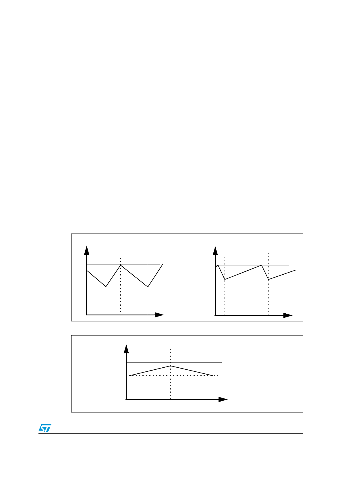
geometric approach will reveal this as shown in Figure 1. A typical variation in average
current vs duty cycle at a given peak current reference is shown in Figure 2.
Figure 1. Peak current regulation at different duty cycles with BEMF load
I
phase
I
peak
I
phase
I
peak
tt
Figure 2. I
vs duty cycle at a given I
ave
I
ave
I
peak
peak
dutycycle
00.51.0
3/19
Page 4
Obtaining the average current AN2267
2 Obtaining the average current
For linear torque control, it is important that we sample the average phase current as
feedback to the current regulator. It is best to get this information from the DC link current
using only a shunt resistor because of its low cost and simplicity. However, the DC link
current is not continuous and is present only during PWM on time. As a simple model for
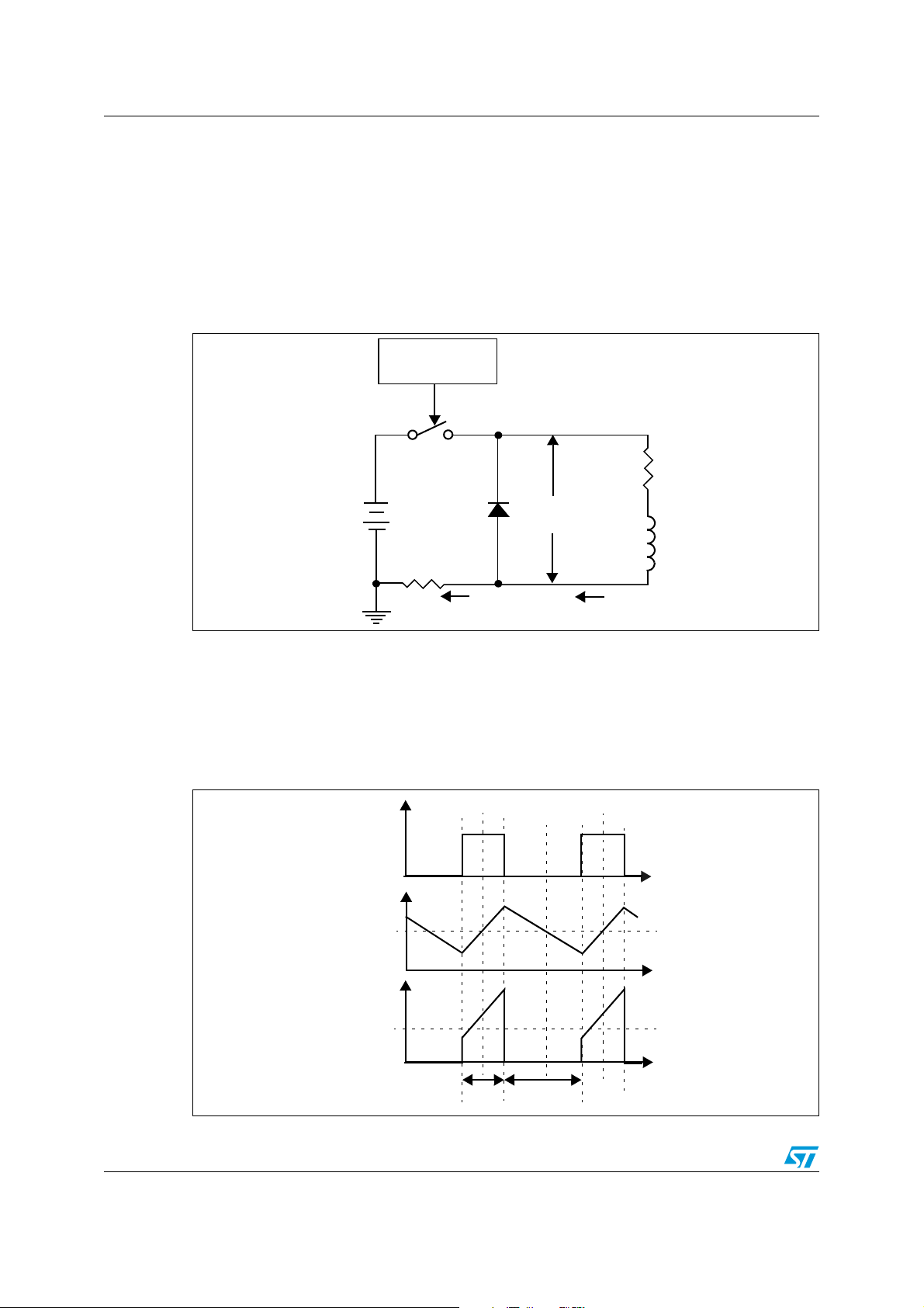
current control, assume a simple buck converter feeding an RL load as shown in Figure 3.
Figure 3. Buck converter feeding an RL load
PWM
CONTROL
SW1
1
BT1
2
R1
D1
V
L
R
sh
I
sh
I
L
L1
The switching frequency, PWM on time and load inductance are such that the load current is
continuous. Figure 4 shows the load voltage, load current and DC link current waveforms. A
close look at the load current waveform reveals that its average value is equal to its
instantaneous value during the middle of PWM on time or off time. Since the load current
flows through the DC link during PWM on time, sampling the DC link current during the
middle of PWM on time gives the average load current.
Figure 4. Buck Converter - Waveforms
V
I
L
I
L(ave
I
S
4/19
T
o
T
off
Page 5
AN2267 BLDC motor control using ST7FMC
(
g
C
g
d
3 BLDC motor control using ST7FMC
The main feature of ST7FMC is its powerful motor control macro cell, capable of generating
control signals to drive a sensorless or sensored 3 phase BLDC or AC motor.
STMicroelectronics application notes AN1946 [1] and AN2030 [2] explain, in detail, the
procedure to control a 3 phase BLDC motor using ST7FMC.
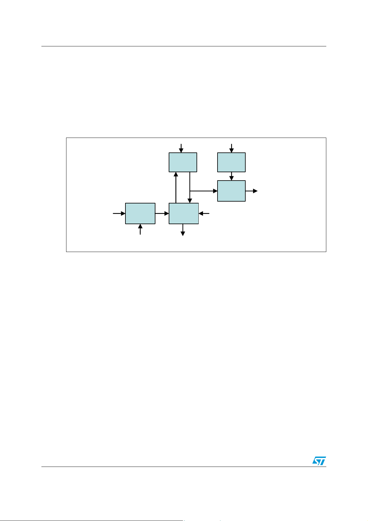
Figure 5 shows the simplified block diagram of the hardware motor control macro cell. The
macrocell has multiple timers performing various functions in parallel to generate control
pulses for the motor. An auto scalable 8-bit timer (MTIM) monitors the time difference
between successive phase back EMF zero crossings (Z events) of the motor. When a Z
event occurs, the timer value is captured into MZREG and the timer restarts counting from
zero, and, the previous content of MZREG is transferred to MZPRV. This timer is a part of
what is called DELAY MANAGER that, based on this time difference and a delay coefficient
(MWGHT), identifies the timing for next phase commutation instant (C events). All in
parallel, a 12-bit free running counter generates the PWM carrier for inverter switching.
Figure 5. Simplified block diagram of Motor control Macro cell for BLDC motors
or SPEED MEASURE UNIT (not
WEIGH
DELAY = WEIGHT x
MEASUREMENT
WINDOW
GENERATOR
PWM
12-bit
Phase
Phase V
Phase W
[Z] : Back EMF Zero-crossin
: Time elapsed between two consecutive Z
Z
n
[C] : Commutation
: Time delayed after Z event to generate C
n
(I): Current
e
(V): Volta
DELAY
(I
CAPTURE
(V
Phase
CURRENT
VOLTAGE
MOD
(V
MTI
TIME
=
COMMUTE
PCN
BEMF ZERO-CROSSING
BEMF=
[Z
TACH
Encoder
INPUT DETECTION
P
H
A
U, V,
Phase
CFAV
CHANNEL
12-bit THREE-PHASE
PWM GENERATOR
Vre
OAON
MCI
MCI
MCI
Ex
In
+
-
AD
MCO
MCO
MCO
MCO
MCO
MCO
NMCE
MCAO
MCAO
MCCRE
C
MCPWM
MCPWM
MCPWM
MCVRE
MCAOZ/
MCCFI
(V
Vd
I
R
3
5/19
Page 6
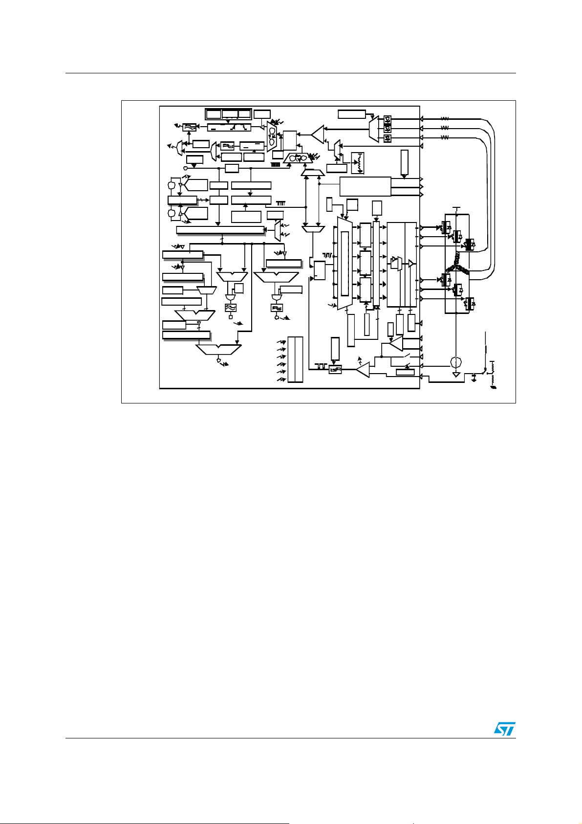
BLDC motor control using ST7FMC AN2267
Figure 6. Motor Control Macro cell - BLDC motor control configuration
HV
C
C
ext
Board + Motor
MCPWMU / V/ W
V
DD
(I)
R
(V)
R
1ext
2ext
Microcontroll er
Z
H
D
H
Fcpu
+1
ST3-0 bits
-1
Z
H
MZREG Reg [ Zn]
Z
S,H
MZP RV Reg [Z
DCB bit
MWGHT R eg [a
SWA bi t
MCOMP Reg [C
EF[2: 0]
Filte r / D
SR bit
X T16 bi t
+
R
MTIM
= FFh?
MZREG
< 55h?
-
R
MTIM [8-bit Up Counter]
]
n-1
]
n+1
A x B / 256
n+1
+
-
S,H
D
S,H
D
V
REF
VR2- 0
SR b it
S,H
Filt er / PWM
Reg
MPHST
CFF[2:0] bit
ISn bit
12- bit P WM ge nera tor
n
bits
OS
MREF
3
n
6 6
Reg
Ch0Ch1Ch2Ch3Ch4
Dead
Time
Dead
Time
High Frequency Chopper
Dead
Time
Ch5
8
2
6
PCN bi t =0
DTG register
MPAR Reg
+
CL
-
x6 x6
AO bit
+
-
CFA V bi t
MCIA
MCIB
MCIC
MCVREF
MPWME Reg
MCPWMU
MCPWMV
MCPWMW
MCO0
MCO2
MCO4
MCO1
MCO3
MCO5
1
NM CE S
MOE bi t
MPOL Reg
MCAOP
MCAON
MCAOZ
MCCFI
MCCREF
B
A
A
CP Bn bit
1 / 2
1 / 2
nn-1
88
Compare
EF[2:0]
Filter / C
Rat i o
ck
C
HDMn bit
1 / 4
8
Compare
S,H
ororor
SA3- 0 &
OT1-0 bits
SZn
bit
Z
S
PZ bit
1 ¾ 1/128
Filter / C
EF[2 :0]
or
CP Bn bit
1 /20
REO bi t
cl r
D
S,H
C
2
1
SPLG
SWA bi t
1
0
D
H
MDREG Reg [ Dn]
Com p a re
SDMn bit
EF[2:0 ]
F ilter / C
CL
-/+
R
E
Z
S,H
D
S,H
C
S,H
S,H
DQ
CP
C
2
1
V
I
Com p ar e U
Z
V
I
C
H
SQ
R
D
S
MISR R eg
MI MR Reg
ZVD bit
4
8
]
A PWM output is generated as a result of comparison between this carrier and a compare
register (MCPUH:MCPUL) that carries pulse width (duty cycle) information. This PWM
signal is directed to one of the six inverter switches by a CHANNEL MANAGER that acts as
a traffic diverter on the PWM output. The channel manager also selects a complementary
switch, as programmed by the user, which together with the switch receiving PWM will force
current into the motor windings. Based on the motor terminal voltages or Hall sensor
outputs, an analog block identifies the motor phase BEMF Z events and captures the
contents of MTIM timer into MZREG and the previous value of MZREG into MZPRV and this
cycle repeats all over again.
6/19
Page 7

AN2267 Implementation using ST7FMC
4 Implementation using ST7FMC
A typical schematic block diagram of ST7FMC based sensorless control of BLDC motor [2]
is shown in Figure 7. Refer to Appendix C on page 16 for a complete schematic of the
experimental hardware. This schematic resembles the motor control starter kit schematic
from Softec Microsystems, with matching I/O assignments wherever possible.
Figure 7. Schematic block diagram of ST7FMC based sensorless control of BLDC
motor
V
V
CC
Speed Ref
AINy
MCO0
MCO1
MCO2
MCO3
MCO4
MCO5
Shut Down
dclink
BLDC
AINx
PE0
PE1
PE2
MCIA
MCIB
MCIC
V
CC
Max Current
ST7FMC
Limit
Figure 8a shows the PWM carrier configured in center aligned mode, where the counter
counts up to a maximum value (as defined by MCP0) and starts counting down to zero and
repeats this cycle again. (See Appendix A for information on setting the PWM frequency).
The PWM generator is set to generate a duty cycle update interrupt (U event) upon
completion of every N carrier cycles as specified by MREP register. (See Appendix A for
information on setting the periodicity of this interrupt). The timing of the U event or interrupt
is positioned as shown in Figure 8a. The carrier is compared with MCPU and PWM pulses
are generated as shown in Figure 8b. Due to the application of PWM voltage on motor
windings, a current flows in its windings as shown in Figure 8c.
7/19
Page 8

Implementation using ST7FMC AN2267
Figure 8. PWM on time midpoint identification and control
MCP0
U event
Carrier
U event
Ref
Fig 8a
t
Fig 8b
PWM
t
Fig 8c
Current
t
Fig 8d
U ISR
t
T
From Figure 8a and Figure 8b, it is clear that the U event takes place at the center of PWM
on time. Based on the previous discussions, this is the right instant to read the
instantaneous DC link current in order to get the average phase current value. Hence the
interrupt associated with U event should be set to the highest priority and the very first
instruction in this Interrupt Service Routine (ISR) should read the DC link current value. In
any case, there is an interrupt latency time of approximately 3-4µs, which is also the typical
conversion time of on-chip Analog to Digital Converter (ADC). If the current feedback analog
input channel was previously selected and set for sampling continuously, then, when the first
instruction in U event interrupt subroutine reads the ADC data register, it will aptly hold the
DC link current value fairly close to that during the middle of PWM on time.
8/19
Page 9

AN2267 Implementation using ST7FMC
Figure 9. Update (U) event interrupt subroutine flow chart
Start U
Read current feedback
Set U ISR priority lower if required
Read other Analog inputs
Current loop PI regulator
Dutycycle update
Set ADC Channel back to Sample current feedback
Restore ISR priority to the highest
End U
The flowchart in Figure 9 shows the actions within the U event interrupt service routine. To
coordinate the reading of any other analog inputs to the ADC, it is recommended that they
are all read within this U event subroutine after the DC link current read. However, before
returning from the interrupt, it is important to restore the ADC to sample the DC link current
channel again so that on re-entry in the next U event, the DC link current value can be read
from ADC right away. If required, interrupt priority of this routine can be lowered after
reading the current value upon entry, but should be restored to the highest value before
returning for obvious reasons.
Refer to the accompanying file for a complete listing of the code and experimental
workspace.
9/19
Page 10

Results AN2267
ω
ω
5 Results
Experimental implementation of this scheme yielded satisfactory results. A closed loop
regulator for BLDC motor control with inner current and outer speed loops as shown in
Figure 10 was implemented. Current loop sampling time of 500µs and speed loop sampling
time of 2ms was chosen. The amount of computing time required within a 2ms time window
to execute through a full cycle of control loop and all motor control ISRs at an electrical
frequency of 200Hz is less than 1ms. The important waveforms obtained are shown in
figures 11 and 12. Figure 11 shows the convergence of reference and actual phase current
values at the instant of occurrence of U event which is the feedback sampling instant. Notice
that the U event occurs during the middle of PWM ON time. Figure 12 shows the tight
control of motor average phase current for a given current reference.
Figure 10. Closed loop current and speed control - block diagram
ST7FMC controller
PI reg
+
-
I*
+
-
Vdclink
PI reg
duty
BLDC
Speed
estimator
10/19
Page 11

AN2267 Results
Figure 11. DC link current sampling at U event and closed loop convergence
Figure 12. Tight control of average phase current vs reference
11/19
Page 12

Conclusion AN2267
6 Conclusion
The experiments performed based on the described method gave fairly linear current
control. One limitation of this sampling method is when the motor current becomes
discontinuous, in which case the actual average current is less than the instantaneous value
at the mid point of PWM on time, and correcting this error is quite cumbersome.
12/19
Page 13

AN2267 References
7 References
[1]. STMicroelectronics AN1946 - Sensorless BLDC motor control and BEMF sampling
methods with ST7MC
[2]. STMicroelectronics AN2030 - Back EMF detection during PWM on time by ST7MC
13/19
Page 14
Sampling inner current loop procedure AN2267
p
Appendix A Sampling inner current loop procedure
Procedure to set carrier frequency (Fpwm) and periodicity of U event (TU) for sampling inner
current loop:
Chosen F
where,
F
pwm
pwm
= F
= 16KHz
/ (Prescaler . 2 . MCP0)
mtc
F
mtc
Prescaler Up/ Down
MPCR
PCP[2:0]
Given F
and choosing Prescaler = 1,
then,
Choosing TU = 500µS
where,
= 16MHz,
mtc
MCP0 = 500
TU = Tpwm . (MREP + 1) / 2
UU
MCP0 MREP
counter
F
wm
Repeat
Counter
MPCR
CMS = 1
U
Substituting for TU and T
pwm
,
MREP = 15
14/19
Page 15

AN2267 Event U interrupt service routine
Appendix B Event U interrupt service routine
/***************************************************
Motor control - Event U interrupt service routine
***************************************************/
@interrupt @nosvf void mtcU_CL_SO_ISR(void)
{
if (bitTest_TRUE(MISR, PUI) ) // check for U event presence
{
/* === Current loop PI Controller begins here === */
currentFb = (ADCDRMSB << 2) + ADCDRLSB; // get new value of currentFb
piconCur(); // call current loop PI regulator
to get new dutycycle
MCPUL = PIconCur.byte.b2; // update MCPUH :MCPUL with new dutycycle
MCPUH = PIconCur.byte.b3;
/* === Current Loop PI controller ends here === */
// Read potentiometer to get latest speed reference
getADC_10bit (speedRef , SPEED_REF_CHNL);
if (speedRef > SPEED_REF_MAX)
speedRef = SPEED_REF_MAX;
// Current Feedback measurement setup for next cycle
ADCCSR = ADON + CURRENT_FDBK_CHNL;
ADCDRMSB; // to clear EOC of prev conv
MISR = 0xff - PUI; //reset IT flag
}
return;
}
15/19
Page 16

ST7MC 3-phase motor control schematics AN2267
Appendix C ST7MC 3-phase motor control schematics
Figure 13. Schematic 1 of 3
of
33Tuesday, January 03, 2006
33Tuesday, January 03, 2006
33Tuesday, January 03, 2006
1
C28
0.1uF
C28
SW DIP-2
SW DIP-2
R52
10K
R52
10K
TP1TP1
1
29
30
32
39
40
MCCREF / PC4
MCPWMV / PC6
PF1 / MCZEM / AIN9
PF0 / MCDEM / AIN8
AIN6 / MCCFI1 / OAZ
OSC15OSC2
6
Y1
16.00MHzY116.00MHz
Ceramic
resonator
PB2PB2
12
C360.1uF C360.1uF
12
R68
R68
470K
470K
+5V
0.1uF
SW6
SW6
+5V
5K
RV45KRV4
Idc1
VcVbVa
Vref
26
20
17
18
19
MCIB / PB2
MCIC / PB3
MCVREF / PB0
AIN5 / MCCFI0 / PC1
(HS) PC025ARTIC2 / PA615ARTCLK / (HS)PA4
13
60
SW1
SW4
SW2
SW3
+5V
2
1
P8P8
R80
10K
R80
10K
C470.1uF C470.1uF
CHBLSHUTDOWN
CL
(HS)MCO53(HS)MCO42(HS)MCO31(HS)MCO264(HS)MCO163(HS)MCO0
MCIA / PB1
AIN0 / PWM0 / PA3
AIN1 / ARTIC1 / PA5
PE5 /
12
14
Temprtr
C38
0.1uF
C38
0.1uF
Vdclink
RV3
RV1
RV2
12
R75
R75
100E
100E
C C
+5V
0.1uF
0.1uF
62
16
Idc
2
3
4
5
R54
10K
R54
10K
R64
R64
12
SIG20
SIG21
J3
ICC Interface
D D
R50
R50
10K
10K
12
10K
10K
R72
R72
CON10AJ3CON10A
1 2
U2
U2
J1J1
1 2
10K
10K
C32
C32
Vpp/
50
61
12
10K
10K
R73
R73
3 4
5 6
7 8
9 10
+5V
R51
R51
22pF
22pF
27
PD5/AIN15 / ICCDATA
49
51K
51K
28
OAP / PC2
OAN / PC3
PD4 / EXTCLK_A / AIN14 / ICCCLK
RESET
38
U4
+5V
AHBHAL
4
MCES
AIN2 / PA7
MISO / PB421AIN3 / MOSI / PB5
SIG5
SIG17
GREEN
GREEN
R60
R60
0.1uF
0.1uF
RV3 5KRV3 5K
0.1uF
0.1uF
RV2 5KRV2 5K
0.1uF
0.1uF
RV1 5KRV1 5K
C41
C41
P5
30V
30V
D33
D33
43
NEC2501U4NEC2501
12
R69
200E
R69
200E
RV3
SIG19
+5V
33
52
51
31
PD6(HS) / RDI
PD7(HS) / TDO
MCPWMU / PC5
PC7 / MCPWMW / AIN7
SCK / (HS) PB623AIN4 / SS/(HS)PB7
Vdd_254Vss_253Vss_1
VAREF
22
34
24
+5V
SIG7
SIG6
D26
RED
D26
RED
D27
D27
470E
470E
R61
680E
R61
680E
C44
C44
C43
C43
C42
C42
594837261
D32D32
R57
R57
1K5
1K5
R58
R58
1K5
1K5
D28D28
12
U3
43
R59
R59
2K2
2K2
C34
C34
680pF
680pF
Vdd_18Vdd_037Vss_036Vss_A
7
35
R83
20K
R83
20K
12
R81
20K
R81
20K
12
+5V
R82
20K
R82
20K
12
R74
20K
R74
20K
12
DB9P5DB9
D29D29
8K2
8K2
R62
R62
8K2
8K2
R63
R63
NEC2501U3NEC2501
st72mc_qfp64
st72mc_qfp64
PE0(HS) / OCMP2_B
55
PE1 / OCMP1_B
56
PE2 / ICAP2_B
57
PE3 / ICAP1_B
58
PE4 / EXTCLK_B
59
PD3 / ICAP1_A / AIN13
48
PD2 / ICAP2_A / AIN12
47
PD1(HS) / OCMP1_A
46
PD0 / OCMP2_A / AIN11
45
PF5 (HS)
44
PF4 (HS)
43
PF3 (HS) / BEEP
42
PF2 / MCO / AIN10
41
PWM1 / PA2
11
PWM2 / (HS) PA1
10
PWM3 / PA0
9
SW2
SW3
SW1
B B
PE0
PE1
PE2
SIG13
SIG12
RV1
OVER_temp
SIG18
RV2
2
1
P7P7
OVER_volt
OVER_cur
SIG4
SIG3
C460.1uF C460.1uF
SIG2
R7910K R7910K
SIG1
SIG20
SIG12
SIG4
SIG19
PE2
+5V
+5V
1 2
P9
SW4
0.01uF
0.01uF
C50
C50
1 2
SW9SW9
0.01uF
0.01uF
C48
C48
1 2
SW8SW8
0.01uF
0.01uF
C49
C49
1 2
SW10SW10
0.01uF
0.01uF
C45
C45
1 2
PB3PB3
PE0
3 4
5 6
7 8
9 10
11 12
13 14
15 16
17 18
19 20
21 22
23 24
25 26
27 28
SIG7
SIG21
SIG18
SIG13
PE1
CD4
CD4
CD2
CD2
CD1
CD1
+5V
CD3
CD3
A A
1
ST7MC control of 3 phase motor
ST7MC control of 3 phase motor
ST7MC control of 3 phase motor
<Doc> 3.0
<Doc> 3.0
<Doc> 3.0
B
B
B
Title
Size Document Number Rev
Date: Sheet of
Title
Size Document Number Rev
Date: Sheet of
Title
Size Document Number Rev
Date: Sheet
2
3
SIG3
SIG1
SIG6
4
29 30
31 32
33 34
HEADER34P9HEADER34
SIG2
SIG5
SIG17
0.1uF
0.1uF
0.1uF
0.1uF
5
0.1uF
0.1uF
0.1uF
0.1uF
16/19
Page 17

AN2267 ST7MC 3-phase motor control schematics
Figure 14. Schematic 2 of 3
of
23Tuesday, January 03, 2006
23Tuesday, January 03, 2006
23Tuesday, January 03, 2006
1
2
1
+15V
P3P3
CP3
CP3
1uF/25V
1uF/25V
CP2
CP2
1uF/25V
1uF/25V
CP1
CP1
1uF/25V
1uF/25V
VA_OUT
VB_OUT
P1P1
VC_OUT
213
+15V
Vdc
+15V
+5V
C27 10uF/25VC27 10uF/25V
3
Vo
GND
L7805U1L7805
2
U1
Vi
1
D215VD21
5V
1
<Doc> 3.0
ST7MC control of 3 phase motor
<Doc> 3.0
ST7MC control of 3 phase motor
<Doc> 3.0
ST7MC control of 3 phase motor
B
B
B
Title
Size Document Number Rev
Date: Sheet
Title
Size Document Number Rev
Date: Sheet of
Title
Size Document Number Rev
Date: Sheet of
2
15v REGULATED SUPPLY
3
D23
D23
4
MAIN
RECTIFIER
5
IC4
IC4
STTA106U
STTA106U
1N4148WS
1N4148WS
D22
D22
680uF/200VC1680uF/200V
4
D7
D7
IR8GBU06
IR8GBU06
F1
2
1
P2
L1
AC POWER IN
SW NEU
D25
D25
18V
18V
100uF/25V
100uF/25V
C31
C31
L1
5
6
7
8
DRAIN
DRAIN
SET
RES
SET
RES
-
+
-
+
VIPER12AS
VIPER12AS
4
VDD
VDD
0.23V
0.23V
FB
FB
3
C26
C26
22uF/25V
22uF/25V
D24
D24
15V
15V
C29
C29
22uF/25V
22uF/25V
0.1uF/400VC20.1uF/400V
C2
R1
R19
R19
100K/2WR1100K/2W
13
C1
W1
W1
POWER_JUMPER
POWER_JUMPER
1
-+
-+
3 2
C20
C20
0.1uF/400V
0.1uF/400V
FUSEF1FUSE
HEADER 2P2HEADER 2
1mHL11mH
SOURCE
SOURCE
C30
C30
C9
0.1uF/400VC90.1uF/400V
100K/2W
100K/2W
22nF
22nF
C13
C13
2
1
LINE
D20
D20
STTA106U
STTA106U
R20
R20
0.015E/2W
0.015E/2W
680uF/200V
680uF/200V
FILTER
N
R8
12
1K
AH
22ER822E
OUT
R45
R45
T2
R9
D2 1N4148WSD2 1N4148WS
10
NC11NC
+15V
D11
1N4148WS
D11
1N4148WS
27K
27K
1K
R271KR27
47ER947E
9
LVG
Vprot
OVER_volt
STGP7NB60HDT2STGP7NB60HD
C4
0.01uFC40.01uF
R10
R10
8
GND
7
C15
C15
1K
R301KR30
OVER_cur
22E
22E
0.1uF
0.1uF
Vdc
T3
R11
47E
R11
47E
D3 1N4148WSD3 1N4148WS
0.47uF/50V
0.47uF/50V
C11
C11
Tantalum
14
D9
STTA106UD9STTA106U
VBOOT
LIN1SD2HIN3VCC4DIAG5CIN6GND
IC2 L6386IC2 L6386
+15V
1K
R281KR28
BL
+5V
C25
C25
+5V
Idc1
13
HVG
STGP7NB60HDT3STGP7NB60HD
C5
0.01uFC50.01uF
R291KR29
J2J2
0.01uF
0.01uF
C33
C33
R12
R12
1K
0.1uF
0.1uF
12
OUT
BH
1 2
T4
D4 1N4148WSD4 1N4148WS
22E
22E
R37
R37
Q1
2N4403Q12N4403
7
-
-
6
NC11NC
+15V
R13
47E
R13
47E
9
10
LVG
D12
1N4148WS
D12
1N4148WS
8K2
8K2
R39
10K
R39
10K
1
R46
51K
R46
51K
84
-
-
2
R40
R40
IC5B
IC5B
TS272
TS272
+
+
5
22E
22E
12
OUT
CH
R47
R47
T6
D6 1N4148WSD6 1N4148WS
NC11NC
+15V
D13
D13
27K
27K
NTC
R2
+5V
Temprtr
R17
47E
R17
47E
10
1N4148WS
1N4148WS
1K
R331KR33
C19
C19
10KR210K
STGP7NB60HDT6STGP7NB60HD
2
C8
0.01uFC80.01uF
R18
22E
R18
22E
9
8
LVG
GND
3
7
4
0.1uF
0.1uF
R341KR34
1K
5
STGP7NB60HDT4STGP7NB60HD
C6
0.01uFC60.01uF
R14
22E
R14
22E
8
GND
7
+5V
R482KR48
2K
PB1PB1
12
1K
R381KR38
C17
0.1uF
C17
0.1uF
IC5A
IC5A
TS272
TS272
+
+
3
1K5
1K5
Vdc
T5
R15
47E
R15
47E
C7
D5 1N4148WSD5 1N4148WS
0.47uF/50V
0.47uF/50V
C12
C12
Tantalum
14
13
D10
STTA106U
D10
STTA106U
HVG
VBOOT
LIN1SD2HIN3VCC4DIAG5CIN6GND
IC3 L6386IC3 L6386
+15V
1K
R311KR31
CL
+5V
C18
1nF
C18
1nF
C16
1nF
C16
1nF
C14
1nF
C14
1nF
R491KR49
1K
SHUTDOWN
STGP7NB60HDT5STGP7NB60HD
0.01uFC70.01uF
R16
R16
1K
R321KR32
OVER_temp
STGP7NB60HDT1STGP7NB60HD
Vdc
T1
R7
47ER747E
C3
0.01uFC30.01uF
D1 1N4148WSD1 1N4148WS
C10
C10
0.47uF/50V
0.47uF/50V
Tantalum
14
13
D8
STTA106UD8STTA106U
HVG
VBOOT
LIN1SD2HIN3VCC4DIAG5CIN6GND
IC1 L6386IC1 L6386
+15V
1K
R251KR25
R261KR26
AL
1%
1%
Idc
+5V
D D
C C
B B
A A
17/19
Page 18

ST7MC 3-phase motor control schematics AN2267
Figure 15. Schematic 3 of 3
of
13Tuesday, January 03, 2006
13Tuesday, January 03, 2006
13Tuesday, January 03, 2006
1
P4
2
R56
R56
4K7
4K7
+5V
R55
R55
4K7
4K7
R53
R53
4K7
VA_OUT
VB_OUT
VC_OUT
4K7
HEADER 5P4HEADER 5
12345
0.01uF
0.01uF
C35
C35
+5V
SW4
SW DIP-3
SW4
SW DIP-3
** SW3 and SW5 are fully CLOSED
1
<Doc> 3.0
ST7MC control of 3 phase motor
<Doc> 3.0
ST7MC control of 3 phase motor
<Doc> 3.0
ST7MC control of 3 phase motor
B
B
B
Title
Size Document Number Rev
Date: Sheet of
Title
Size Document Number Rev
Date: Sheet of
Title
Size Document Number Rev
Date: Sheet
2
R35
470E
R35
R5
180K/2WR5180K/2W
R71
47K
R71
SW5
SW DIP-4
SW5
SW3
SW DIP-3
SW3
1N4148WS
1N4148WS
D17
D17
1N4148WS
1N4148WS
D19
D19
1N4148WS
1N4148WS
1N4148WS
1N4148WS
SW2
SW2
SW DIP-3
SW DIP-4
SW DIP-4
D16
D16
D14
1N4148WS
D14
R22
R22
100K/2W
100K/2W
+5V
1N4148WS
D15
1N4148WS
D15
1N4148WS
R441KR44
1K
R431KR43
1K
R421KR42
1K
R411KR41
1K
D18
D18
R4
180K/2WR4180K/2W
3
R3
180K/2WR3180K/2W
4
R61KR6
1K
R241KR24
1K
R231KR23
1K
5
SW DIP-4
SW1
SW1
Vc
47K
R70
47K
R70
47K
R65
47K
R65
47K
VrefVbVa
SW DIP-4
SW DIP-4
C21
C21
0.1uF
0.1uF
C22
C22
0.1uF
0.1uF
C23
C23
0.1uF
0.1uF
C24
C24
0.1uF
0.1uF
SW7
SW7
+5V
SW DIP-2
SW DIP-2
+5V
PE0PE1PE2
R66
R66
470E
VprotVdclink
R36
39K
R36
39K
R21
R21
330K/2W
330K/2W
Vdc
5K
RV55KRV5
+5V
C39
C39
2.2nF
2.2nF
Q2
2N2222Q22N2222
R76
100E
R76
0(NC)
0(NC)
100E
C40
0.1uF
C40
0.1uF
1N4148WS
1N4148WS
D31
R78
R78
2
D31
10K
10K
D30
D30
1N4148WS
1N4148WS
C37
C37
0.1uF
0.1uF
1
10K
10K
R77
R77
10K
10K
R67
R67
P6P6
3
4
5
D D
C C
18/19
B B
A A
Page 19

AN2267
Please Read Carefully:
Information in this document is provided solely in connection with ST products. STMicroelectronics NV and its subsidiaries (“ST”) reserve the
right to make changes, corrections, modifications or improvements, to this document, and the products and services described herein at any
time, without notice.
All ST products are sold pursuant to ST’s terms and conditions of sale.
Purchasers are solely responsible for the choice, selection and use of the ST products and services described herein, and ST assumes no
liability whatsoever relating to the choice, selection or use of the ST products and services described herein.
No license, express or implied, by estoppel or otherwise, to any intellectual property rights is granted under this document. If any part of this
document refers to any third party products or services it shall not be deemed a license grant by ST for the use of such third party products
or services, or any intellectual property contained therein or considered as a warranty covering the use in any manner whatsoever of such
third party products or services or any intellectual property contained therein.
UNLESS OTHERWISE SET FORTH IN ST’S TERMS AND CONDITIONS OF SALE ST DISCLAIMS ANY EXPRESS OR IMPLIED
WARRANTY WITH RESPECT TO THE USE AND/OR SALE OF ST PRODUCTS INCLUDING WITHOUT LIMITATION IMPLIED
WARRANTIES OF MERCHANTABILITY, FITNESS FOR A PARTICULAR PURPOSE (AND THEIR EQUIVALENTS UNDER THE LAWS
OF ANY JURISDICTION), OR INFRINGEMENT OF ANY PATENT, COPYRIGHT OR OTHER INTELLECTUAL PROPERTY RIGHT.
UNLESS EXPRESSLY APPROVED IN WRITING BY AN AUTHORIZE REPRESENTATIVE OF ST, ST PRODUCTS ARE NOT DESIGNED,
AUTHORIZED OR WARRANTED FOR USE IN MILITARY, AIR CRAFT, SPACE, LIFE SAVING, OR LIFE SUSTAINING APPLICATIONS,
NOR IN PRODUCTS OR SYSTEMS, WHERE FAILURE OR MALFUNCTION MAY RESULT IN PERSONAL INJURY, DEATH, OR
SEVERE PROPERTY OR ENVIRONMENTAL DAMAGE.
Resale of ST products with provisions different from the statements and/or technical features set forth in this document shall immediately void
any warranty granted by ST for the ST product or service described herein and shall not create or extend in any manner whatsoever, any
liability of ST.
ST and the ST logo are trademarks or registered trademarks of ST in various countries.
Information in this document supersedes and replaces all information previously supplied.
The ST logo is a registered trademark of STMicroelectronics. All other names are the property of their respective owners.
© 2006 STMicroelectronics - All rights reserved
STMicroelectronics group of companies
Australia - Belgium - Brazil - Canada - China - Czech Republic - Finland - France - Germany - Hong Kong - India - Israel - Italy - Japan -
Malaysia - Malta - Morocco - Singapore - Spain - Sweden - Switzerland - United Kingdom - United States of America
www.st.com
19/19
 Loading...