Page 1
Introduction
Some industrial applications require a so called 'ultra-wide' input voltage range (between 90
and 450Vac). Due to the variations of the main, input voltages up to 450V ac are typical in threephase applications. A maximum input voltage of 450Vac requires the use of very high voltage
components, increasing cost, size, the weight and the overall complexity of the power supply .
Hence, the market is looking for solutions with low cost and good performance.
Thi document introduces a cost effective solution for low power high voltage power supplies.
The proposed solution consists of in an off-line SMPS and a low cost front-end regulation circuit
for input voltage limiting. Such a circuit allows proper operation of the power converter avoiding
the use of voltage over-rated components, both passive and active. The circuit is suitable for
any off-line SMPS topology since it includes a switching transistor connected between the input
rectifier and the DC bulk capacitor (STMicroelectronics patent pending). The series switch
limits the DC input voltage of the power converter by means of a suitable driving circuit; thus
the SMPS primary transistor can be selected as a standard part as well as a smart power
primary IC.
AN2264
APPLICATION NOT E
Three-Phase SMPS for low power applications
with VIPer12A
Typical end applications of this solution can be found in the industrial market in the range below
5W, such as three-phase and single phase power meter, industrial bias power supply and
auxiliary S MPS for high vo ltage stree t-lighti ng, where the input voltage can range between
90Vac and 450Vac and 1000V power MOSFETs are currently used.
As an example of industrial applications, a flyback converter for supplying an electronic power
meter is considered. The use of the proposed approach in a power converter designed for
265Vac maximum input voltage allows the operating input voltage to be extended up to 450Vac
or higher with no damages to the converter components. Thus, the major benefit of such
solution is a significant cost saving thanks to the reduction of components voltage rating.
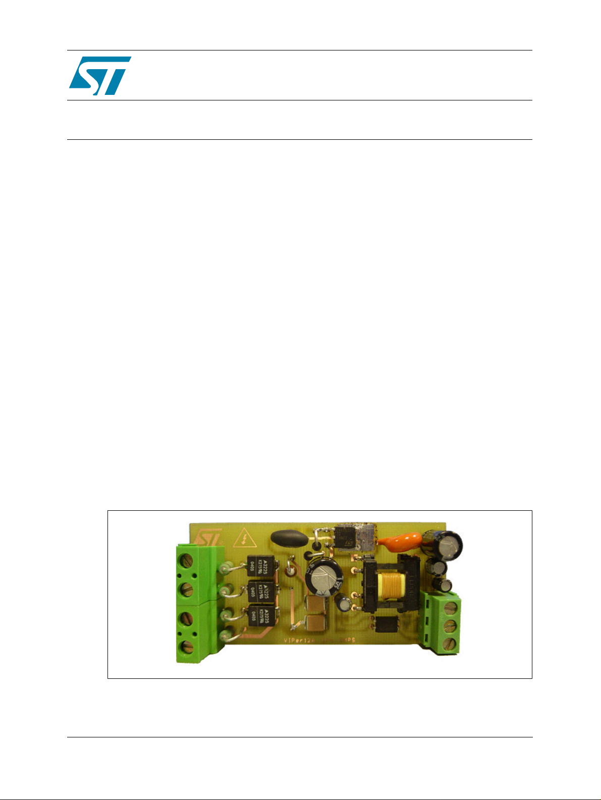
Figure 1. Board Prototype
Rev 1.0
AN2264/1105 1/42
www.st.com
42
Page 2

AN2264
Contents
1 Application Description . . . . . . . . . . . . . . . . . . . . . . . . . . . . . . . . . . . . . . . . 5
2 Circuit Description . . . . . . . . . . . . . . . . . . . . . . . . . . . . . . . . . . . . . . . . . . . . 7
3 Experimental Results . . . . . . . . . . . . . . . . . . . . . . . . . . . . . . . . . . . . . . . . . 13
3.1 Input Voltage Limiting Circuit . . . . . . . . . . . . . . . . . . . . . . . . . . . . . . . . . . . . 13
3.2 Steady State Behaviour . . . . . . . . . . . . . . . . . . . . . . . . . . . . . . . . . . . . . . . . . 14
3.3 Line And Load Regulations . . . . . . . . . . . . . . . . . . . . . . . . . . . . . . . . . . . . . . 28
3.4 Hold-up Time Capability . . . . . . . . . . . . . . . . . . . . . . . . . . . . . . . . . . . . . . . . 29
3.5 Additional Considerations . . . . . . . . . . . . . . . . . . . . . . . . . . . . . . . . . . . . . . . 30
3.6 Measurements At The Start-Up . . . . . . . . . . . . . . . . . . . . . . . . . . . . . . . . . . 31
4 Conducted Emissions Test . . . . . . . . . . . . . . . . . . . . . . . . . . . . . . . . . . . . . 34
5 Thermal Measurements . . . . . . . . . . . . . . . . . . . . . . . . . . . . . . . . . . . . . . . 36
6 Conclusions . . . . . . . . . . . . . . . . . . . . . . . . . . . . . . . . . . . . . . . . . . . . . . . . . 39
7 Revision History . . . . . . . . . . . . . . . . . . . . . . . . . . . . . . . . . . . . . . . . . . . . . 40
2/42
Page 3

AN2264
Figures
Figure 1. Board Prototype . . . . . . . . . . . . . . . . . . . . . . . . . . . . . . . . . . . . . . . . . . . . . 1
Figure 2. Circuit Schematic . . . . . . . . . . . . . . . . . . . . . . . . . . . . . . . . . . . . . . . . . . . . 8
Figure 3. PCB Layout. . . . . . . . . . . . . . . . . . . . . . . . . . . . . . . . . . . . . . . . . . . . . . . . . 9
Figure 4. Flyback Transformer . . . . . . . . . . . . . . . . . . . . . . . . . . . . . . . . . . . . . . . . . 10
Figure 5. MOSFET STD3NK50Z Operation at FULL LOA D and Vin = 450 Vrms . . 13
Figure 6. VIPer12AS Vds & Id at FULL LOAD . . . . . . . . . . . . . . . . . . . . . . . . . . . . . 14
Figure 7. VIPer12AS Vds & Id at HALF LOAD. . . . . . . . . . . . . . . . . . . . . . . . . . . . . 18
Figure 8. VIPer12AS Vds & Id at MINIMUM LOAD . . . . . . . . . . . . . . . . . . . . . . . . . 22
Figure 9. STD3NK50Z Vds & Id at FULL LOAD . . . . . . . . . . . . . . . . . . . . . . . . . . . . 26
Figure 10. Line Regulation . . . . . . . . . . . . . . . . . . . . . . . . . . . . . . . . . . . . . . . . . . . . . 28
Figure 11. Load Regulation . . . . . . . . . . . . . . . . . . . . . . . . . . . . . . . . . . . . . . . . . . . . 28
Figure 12. Hold-up Time Capability at FULL LOAD. . . . . . . . . . . . . . . . . . . . . . . . . . 29
Figure 13. Waveforms . . . . . . . . . . . . . . . . . . . . . . . . . . . . . . . . . . . . . . . . . . . . . . . . 30
Figure 14. VIPer12AS and Outputs-Start-up at FULL LOAD . . . . . . . . . . . . . . . . . . . 31
Figu r e 1 5 . STD3N K 5 0 Z-1 St a r t-up at FULL LOAD . . . . . . . . . . . . . . . . . . . . . . . . . . 32
Figure 16. Start-up at MINIMUM LOAD . . . . . . . . . . . . . . . . . . . . . . . . . . . . . . . . . . . 33
Figure 17. Conducted Emissions - at Vin=230Vac - FULL LOAD . . . . . . . . . . . . . . . 34
Figure 18. Conducted Emissions - at Vin=380Vac - FULL LOAD . . . . . . . . . . . . . . . 35
Figure 19. Thermal Measurements . . . . . . . . . . . . . . . . . . . . . . . . . . . . . . . . . . . . . . 37
3/42
Page 4

AN2264
Tables
Table 1. Operating conditions . . . . . . . . . . . . . . . . . . . . . . . . . . . . . . . . . . . . . . . . . . 5
Table 2. Three-Phase Electricity Meter Voltage Marking . . . . . . . . . . . . . . . . . . . . . 5
Table 3. B ill of Materials . . . . . . . . . . . . . . . . . . . . . . . . . . . . . . . . . . . . . . . . . . . . . 11
Table 4. Full Load (Iout ≈100mA) . . . . . . . . . . . . . . . . . . . . . . . . . . . . . . . . . . . . . . 16
Table 5. Half Load (Iout≈50mA) . . . . . . . . . . . . . . . . . . . . . . . . . . . . . . . . . . . . . . . 20
Table 6. Minimum Load (Iout=10mA). . . . . . . . . . . . . . . . . . . . . . . . . . . . . . . . . . . 24
4/42
Page 5
AN2264 1 Application Description
1 Application Description
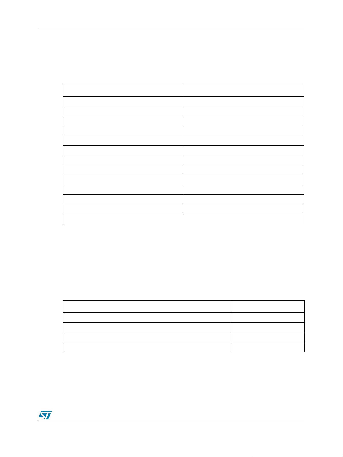
The present SMPS has been designed according to the following specifications:
Table 1. Operating conditions
Parameter Value
Input Voltage Range 90 to 450 V ac
Input Frequency Range 50/60 Hz
Output Voltage 1 V1=5V
Output Voltage 2 V2=3.3V
Output Current 1 I1=10mA
Output Current 2 I2=100mA
Output Power (peak) 550mW
Line Regulation +/- 1%
Load Regulation +/- 1%
Output Ripple Voltage 1 50mV
Hold-up capability > 40 ms (*)
Safety EN60950
EMI EN55022 class B
(*) Considering the STPM01 roll over time (31ms) and the Memory M95040 write time per data
(5ms).
In addition to the previous specs, the power supply has to be compliant also with the standards
of electricity meters, i.e. IEC 62052-11 and IEC 62053-21, since it has been specifically
developed for such an application. The main prescriptions are listed here below:
● Input connection and voltage marking (EN62052-11):
Table 2. Three-Phase Electricity Meter Voltage Marking
Meter Rated System Voltage (V)
Single-phase 2 wire 120V 120
Single-phase 3 wire 120V (120V to t he mid-wire) 240
Three-Phase 3 wire 2-element (230 V between phases) 400
Three-Phase 4 wire 3-element (230 V phase to neutral) 400
● Pulse Voltage Test (EN62052-11):
- Pulse waveform: according IEC 60060-1
- Voltage rise time: ±30%
- Voltage fall time: ±20%
5/42
Page 6

1 Application Description AN2264
- Source impedance: 500Ω ± 50Ω
- Source Energy: 0.5J ±0.05J
- Rated Pulse Voltage: 4000V
- Test Voltage Tolerance: +0 -10%
● Mean input power : 2W according to EN62053-21 (Switching power supplies with peak
power values exceeding the specified value are also permitted)
● Temperature Range: -25°C ± 3°C ÷ +70°C ± 2°C (EN 62052-11)
6/42
Page 7

AN2264 2 Circuit Description
2 Circuit Description
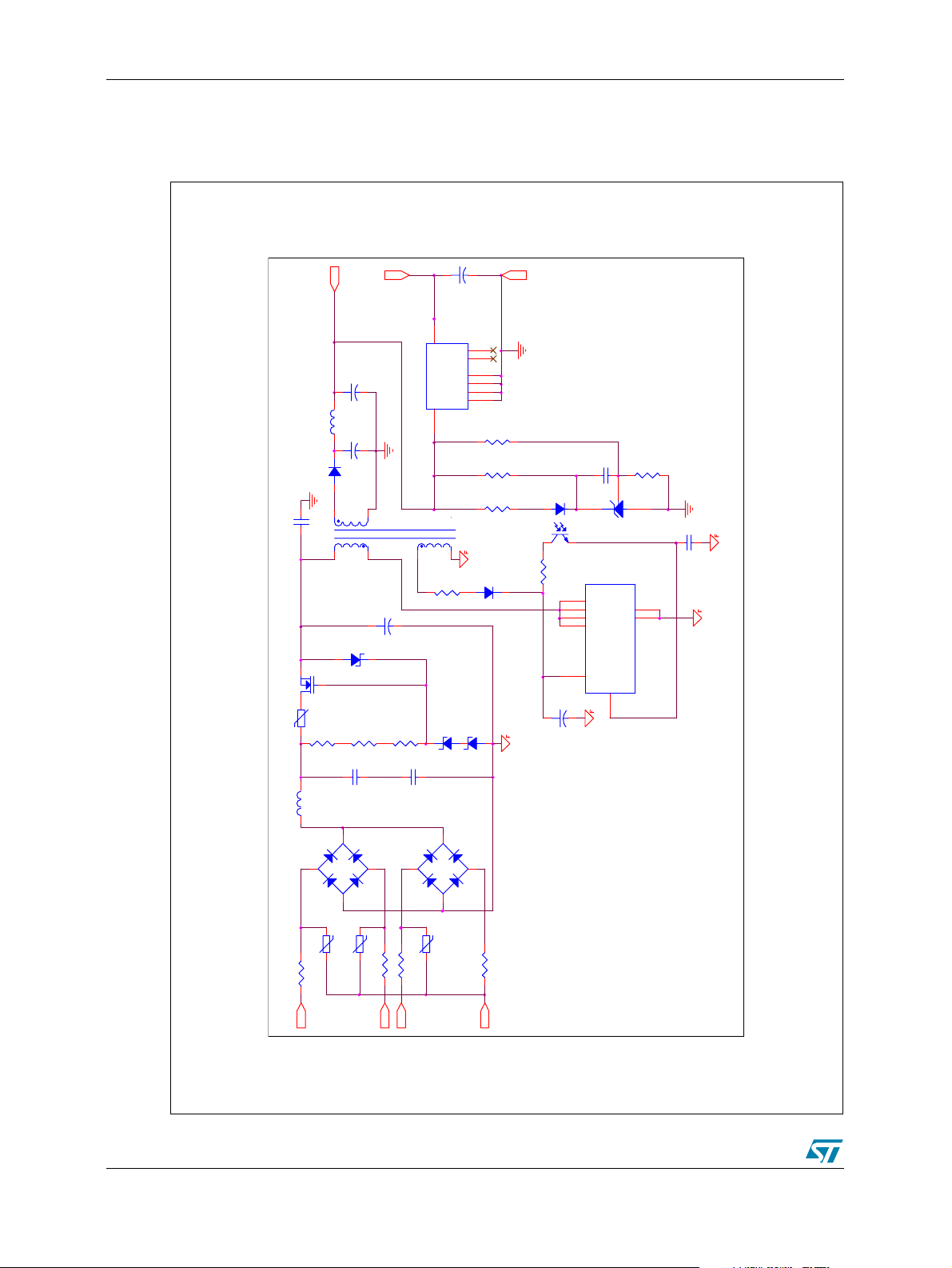
The schematic of the board is shown in Figure 2.
A 3-phase 4-wire bridge is used for mains rectification because the neutral rectification is
needed to ensure proper operation in case of missing neutral connection or neutral mis-wiring.
A varistor is connected between each line and neutral to guarantee pulse voltage test immunity
according to the EN62052-11 standard.
The input EMI filter is a simple undamped LC-filter for both differential and common mode noise
suppression.
The circuit for input voltage limiting is connected between the input EMI filter and the bulk
capacitor C4. Such a circuitry includes a Power MOSFET and a self driven control section.
The MOSFET Q1 is a standard N-Channel 500V 3.3Ω in D-PAK package, mounted on a small
copper area to improve thermal performance. The self driven control section consists of a
voltage divider and zener diodes. The resistors R1, R2 and R3 ensure the gate-source charge
for the switch, while the zener diodes D3 and D4 set t he maximum voltage val ue (360V) ac ross
the bulk capacitor.
An NTC limits the inrush current and ensures Q1 operation inside its safe operating area.
The flyback converter is based on VIPer12AS, a member of the VIPerX2A family, which
combines a dedicated current mode off-line PWM controller with a high voltage power
MOSFET on the same silicon chip. The switching frequency is fixed at 60kHz by the IC internal
oscillator allowing, to optimize the transformer size and cost. The transformer reflected voltage
has been set to 60V, providing enough margin for the leakage inductance voltage spike and no
snubber circuit is needed with a consequent cost saving.
As soon as the voltage is applied on the input of the converter the high voltage start-up current
source connected to the drain pin is activated and starts to charge the V
a constant current of 1mA. When the voltage across this capacitor reaches the V
(about 14V) the VIPer12AS starts to switch. During normal operation the smart power IC is
powered by the auxiliary win ding of the transforme r via the diode D7. No spike killer fo r the
auxiliary vo ltage fluctu ations is needed thanks to the wide range of the V
primary current is measured using the integrated current sensing for current mode operation.
The output rectifier D6 has been chosen in accordance with the maximum reverse voltage and
power dissipation; in particular a 0.5A-80V Schottky diode, type TMBAT49, has been selected.
The output voltage regulation is performed by secondary feedback on the 5V output dedicated
to the display, while the 3.3V output, dedicated to the logic part and the microcontroller, is
linearly post-regulated from the 5V output. This operation is performed by a very low drop
voltage regulator, L4931ABD33, in SO-8 package. The voltage regulator delivers up to 100mA,
ensuring good reliability with no heat sink. The feedback netw ork ensures the requir ed
insulation between the primary and secondary sections. The optotransistor directly drives the
VIPer12AS feedback pin which controls the IC operation.
A small LC filter has been added to the 5V output in order reduce the high frequency ripple with
reasonable output capacitors value.
capacitor C8 through
dd
pin (9-38V). The
dd
threshold
ddon
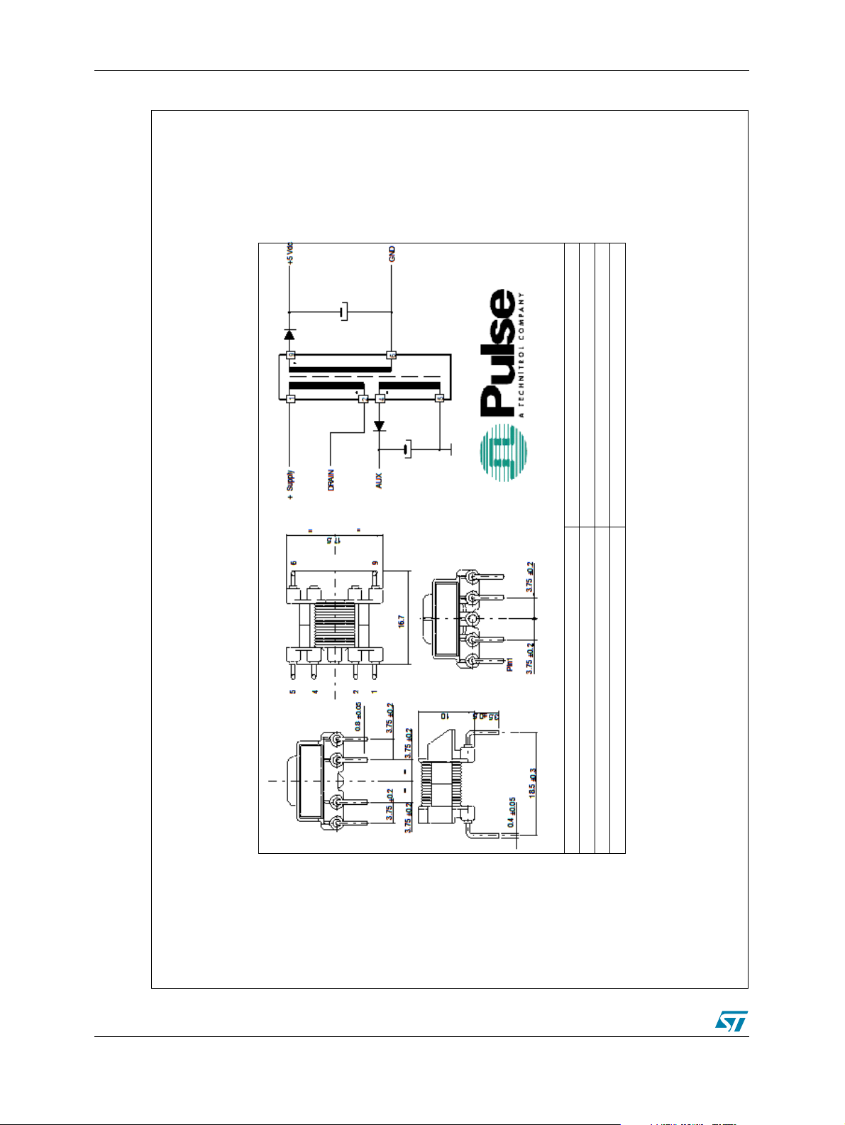
The flyback transformer is a layer type based on E13 core and N27 ferrite, manufactured by
Pulse Eldor, and ensures safety insulation in accordance with the EN60950. Figure 4. shows
the main features of the transformer.
7/42
Page 8
2 Circuit Description AN2264
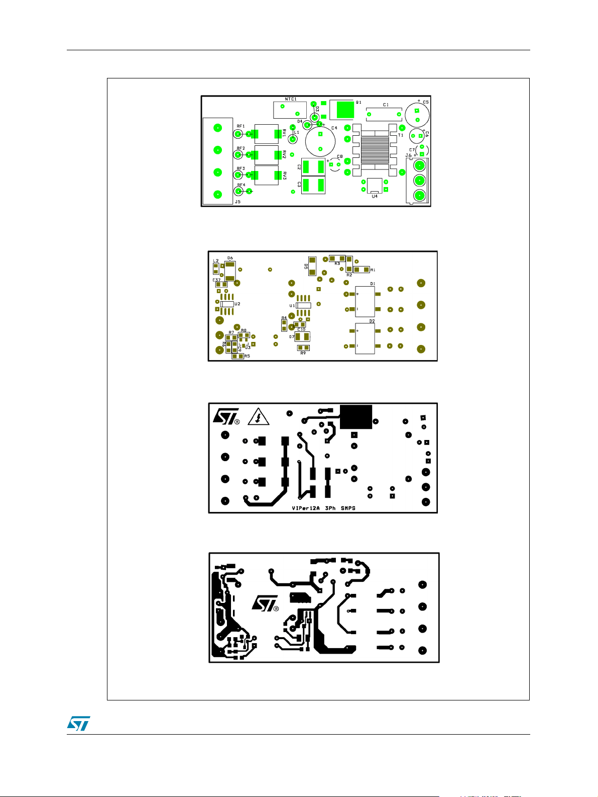
The whole power supply has been realized on a double side 35um PCB in FR-4, measuring 78
x 38 mm.
Figure 2. Circuit Sc hemati c
3.3V@100mA
1
U2 L4931ABD33
8
4
+
R7
R6
R5
LL4148
GND
4.7K
SMD
1K
SMD
12
U4
PC817
43
220E SMD
R9
C8
50V
SMD
R8
C9
100nF
U3
5.6K SMD
D
8
D
7
D
6
D
5
U1
4
+
10uF 50V
4.7K SMD
3
TS2431
2 1
C10
47nF
50V
SMD
S
1
S
2
VIPer12AS
Vdd
FB
3
C7
2.2uF 25V
INH
5
NC
4
VOUT
GND
7
GND
6
GND
3
GND
2
VIN
5
D7
R4
10E
SMD
D4
180V
D3
180V
VDD
5V@10mA
L2
10uH 100mA SMD
D6
TMBAT 49
C1
Q1
NTC1
10
2.2nF/ 2k V (Y1)
T1
1
D5
1
STD3NK50Z
2 3
50E
R1
3.3V
+
C6
22uF 25V
+
C5
330uF 25V
6
2
2.2uF450V
+
C4
SOD-80
ZMM 1 5
R3
330K SMD
330K SMD
R2
330K SMD
D1
2
RV1
SO5K275/275V
P1
C2
220nF
3
-+
4
RV2
SO5K275/275V
L1
1mH
RF1
22E 0.75W
630V
SMD
BRIDGE
RF2
1
22E 0.75W
P2NP3
C3
630V
SMD
220nF
3
D2
2
-+
4
RV3
SO5K275/275V
RF3
22E 0.75W
8/42
BRIDGE
1
RF4
22E 0.75W
Layout Hin ts: Q1 mounted on 1cm x 0.8cm copper
area. C8&C 10 have to be c losed to the VI Per12AS.
GND Pins f or U2 have to b e soldered to a unique
Note:
copper are a.
Page 9
AN2264 2 Circuit Description
Figure 3. PCB La yout
Top side-silk screen (in scale)
Bottom side- silk screen (in scale)
Top side-copper tracks (in scale)
Bottom side-copper tracks (in scale)
9/42
Page 10
2 Circuit Description AN2264
Figure 4. Flyback Tran sformer
< 2%
11
3
):
p
Primary Inductance: 2.2mH ±20%
Primary Leakage Inductance (%L
Primary to secondary turn ratio:
Auxiliary to secondary turn ratio:
10/42
Page 11

AN2264 2 Circuit Description
Table 3. Bill of Materials
Reference Value Description
CON1, CON2
CON3
Hartmann/ptr, 2 poles, type PK 7402, 380V
Hartmann/ptr, 3 poles, type PK 3503, 380V
AC
AC
16A
16A
C1 2.2nF/2kV Cera-Mite Corporation 44LD 22 Y1 Ceramic Capacitor 20%
C2, C3 220nF 630V TDK C5750X7R2J224M SMD Ceramic Capacitor 20%
C4 2.2uF450V
C5 330uF 25V
C6 22uF 16V
C7 2 .2uF 50V
C8 10uF 50V
Rubycon Aluminium Radial Lead El ectrolytic Capacitor YK
Series 29mA 20%
Rubycon Aluminium Radial Lead El ectrolytic Capacitor ZL
Series 56mR 995mA 20%
Rubycon Aluminium Radial Lead El ectrolytic Capacitor ZA
Series 270mR 350mA 20%
Panasonic ECA1HHG2R2 NHG-A Radial Lead Electrolytic
Capacitor 18mA 20%
Panasonic ECA1HHG100 NHG-A Radial Lead Electrolytic
Capacitor 39mA 20%
C9 100nF 50V muRata GRM40X7R104Z50 SMD Ceramic Capacitor 20%
C10 47nF 50V muRata GRM40X7R473Z50 SMD Ceramic Capacitor 20%
D1, D2 BRIDGE General Instrument s DF 10S SMT Diode Bridge 1000V 1A
D3, D4 ZY180V DO-41 Zener Diode 180V 2W 5%
D5 ZMM 15/SOD-80 Mini-Melf Zener Diode 15V 0.5W 5%
D6
TMBAT49 STMicroelectronics Small Signal Schottky Diode 80V 0.5A
D7 LL4148/SOD-80 SOD-80 General Purpose Rectifier 75V 200mA
L1 1mH Epcos B78108-S1105J , Bobbin Core BC 130mA 13R 10%
L2 10uH
TDK GLF2012T100M SMD Signal-Use SMD Inductor 125mA
20%
NTC1 50E UEI 10SP050L Inrush Current Suppr essor 50R 2A 10%
Q1
RF1, RF2, RF3,
RF4
RV1, RV2, R V 3 SO5K275/275V
STD3NK50Z STMicroelectronics N -Channel Mosfet 500V 2.3A 3.3R
22E 0.75W Ya geo R esi stor, wire wound, fusible, 22R 0.75W 5%
Epcos B72650M271K72 SMD Varistor 275V
AC
8.6J
R1, R2, R3 330K SMD Resistor, Metal Film 0.25W 5%
R4 10E SMD Resistor, Metal Film 0.25W 5%
R5 220E SMD Resistor, Metal Fil m 0.25W 5%
R6 1K SMD Resistor, Metal Film 0.25W 5%
R7 4.7K SMD Resistor, Metal Fil m 0.25W 5%
R8 4.7K SMD Resistor, Metal Film 0.25W 5%
R9 5.6K SMD Resistor, Metal Film 0.25W 5%
11/42
Page 12

2 Circuit Description AN2264
Table3. Bill of Materials (Continued)
Reference Value Description
T1 2432.0015C E13 TIW Pulse Eldor Switch Mode Transformer
U1
U2
U3
U4 PC817 Sharp Optocoupler 5kV
VIPer12AS
L4931ABD33
TS2431
STMicroelectronics
27R
STMicroelectronics
3.3V 300mA 1%
STMicroelectronics
Reference 1%
Off Line SMPS Primary IC 730V 0.4A
Very Low Drop Voltage Regulator
Programmable Shunt V ol tage
12/42
Page 13
AN2264 3 Experimental Results
3 Experimental Results
3.1 Input Voltage Limiting Circuit
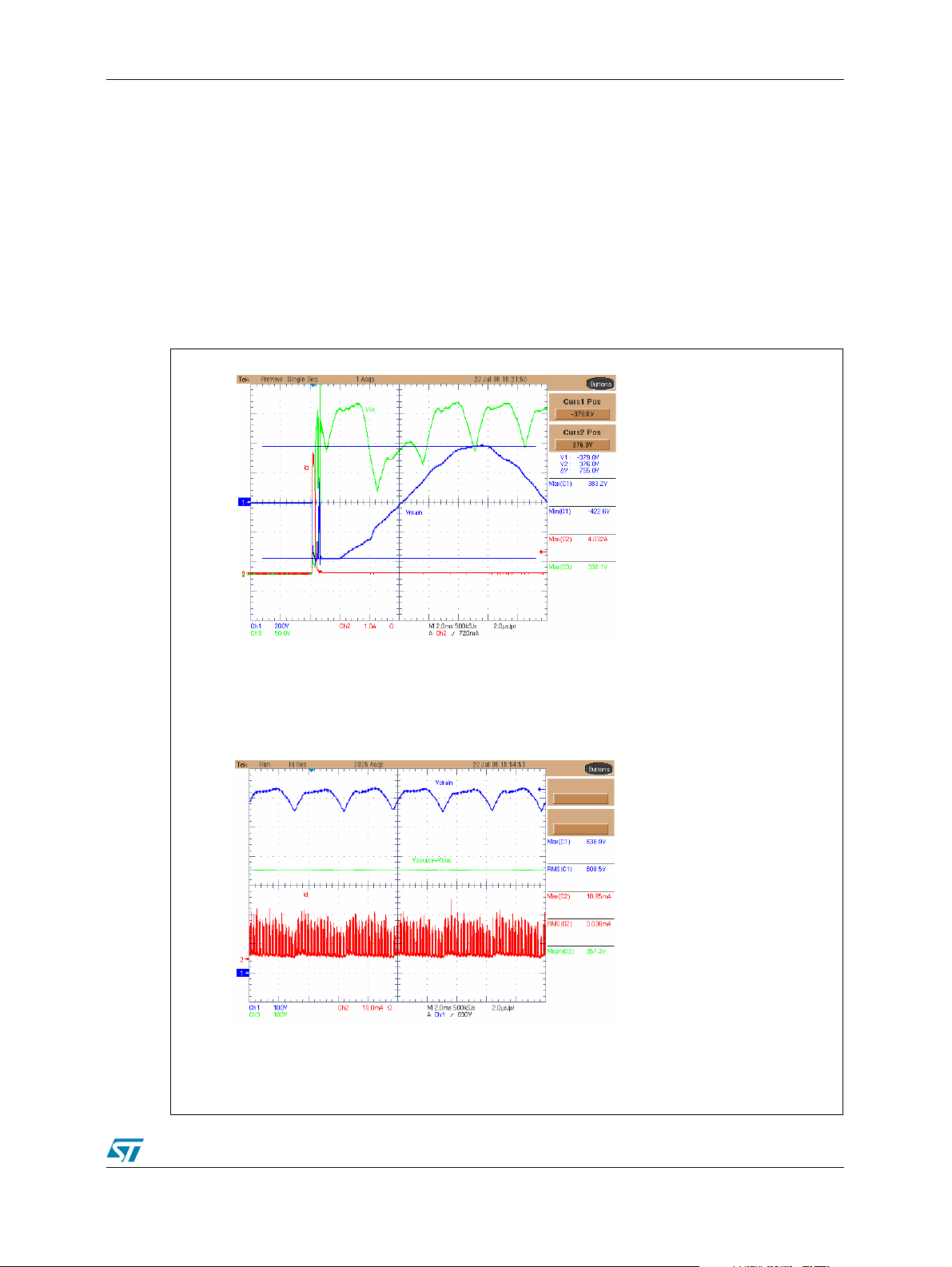
The main waveforms of the input voltage limiting circuit are shown in Figure 5. In particular the
waveforms refer to the start-up and the steady-state operations at 450Vac and full load ,which
are the worst conditions for the device. The advantages of this solution are evident. It limits the
DC voltage at the given reference value, in this case 360V, and avoides the use of over-rated
components compared to the standard off-line power supply.
Figure 5. MOSFET STD3NK50Z Operati on at FULL LOAD and Vin = 450 Vrms
Start-Up
CH1: INPUT VOLTAGE (Blue)
CH2: DRAIN CURRENT (Red)
CH3: DRAIN-SOURCE VOLTAGE (Green)
CH1: DRAIN VOLTAGE (Blue)
CH2: DRAIN CURRENT (Red)
CH3: SOURCE VOLTAGE (Green)
Steady State
13/42
Page 14

3 Experimental Results AN2264
3.2 Steady State Behaviour
Several measurements have been performed on the SMP S in steady state operation, for
different values of the main voltage and load condition. The measured values are:
- The peak Drain Current through the VIPer12A
- The peak Drain Voltage across the VIPer12A
- The Peak Drain Voltage across the input MOS
- The Peak Drain Current through the input MOS
- The Reverse Voltage across the output Diode
- The Output Voltage
- The input power consumption
Figure 6. shows some waveforms during the normal operation at full load:
Figure 6. VIPer12AS Vds & Id at FULL LOAD
Vin=90 Vrms - 50Hz
Vin = 110 Vrms - 50Hz
14/42
Page 15

AN2264 3 Experimental Results
f
t
t
n
s
e
d
Figure 6. VIPer12AS Vds & Id at FULL LOAD (continued)
Vin = 230 Vrms - 50Hz
Vin = 450 Vrms - 50Hz
CH1: DRAIN VOLTAGE (Blue)
CH2: DRAIN CURRENT (Red)
Vin = 380 Vrms - 50Hz
Vin
Vdsmax(V) Idpk(mA)
(Vac)
90 210 122
110 236 120
230 398 138
380 438 152
450 444 148
The table lists the measured values o
the drain peak voltage and current a
minimum, nominal and maximum inpu
mains voltage, during normal operatio
at full load. The voltage peak, which i
444V, assures a reli able opera tion of th
VIPer12AS power switch with a goo
margin against the maximum B
VDSS
.
15/42
Page 16

3 Experimental Results AN2264
Table 4. Full Load (Iout ≈100mA)
Input
Vin [Vrm s]= 90
Iin [mArms ] = 10.7
Pin [W] = 0.93
Output
Vout [V] = 3.303 4.989
Iout [mA] = 100 1
Pout [W] = 0.5
EFF.=54%
Input
Vin [Vrm s]= 110
Iin [mArms ] = 9.2
Pin [W] = 0.93
Output
Vout [V] = 3.303 4.989
Iout [mA] = 100 1
Pout [W] = 0.5
EFF.=54%
Input
Vin [Vrms]= 230
Iin [mArms ] = 6.5
Pin [W] = 1.1 2
Output
Vout [V] = 3.303 4.989
Iout [mA] = 100 1
Pout [W] = 0.5
EFF.=45%
16/42
Page 17

AN2264 3 Experimental Results
Table 4. Full Load (Iout ≈100mA) (continued)
Input
Vin [Vrms]= 380
Iin [mArms ] = 4.4
Pin [W] = 1.6
Output
Vout [V] = 3.303 4.989
Iout [mA] = 100 1
Pout [W] = 0.5
EFF.=31%
Input
Vin [Vrms]= 450
Iin [mArms ] = 4.5
Pin [W] = 2.0
Output
Vout [V] = 3.303 4.989
Iout [mA] = 100 1
Pout [W] = 0.5
EFF.=25%
The same test has been performed on the board in half load condition, for the different values
of the input voltage. In Figure 7. some typical waveforms are shown.
17/42
Page 18

3 Experimental Results AN2264
Figure 7. VIPer12AS Vds & Id at HALF LOAD
Vin = 90 Vrms - 50Hz
Vin = 110 Vrms - 50Hz
Vin = 230 Vrms - 50Hz
18/42
Page 19

AN2264 3 Experimental Results
Figure 7. VIPer12AS Vds & Id at HALF LOAD (Continued)
Vin = 380 Vrms - 50Hz
Vin = 450 Vrms - 50Hz
CH1: DRAIN VOLTAGE (Blue)
CH2: DRAIN CURRENT (Red)
Vin (Vac) Vdsmax(V) Idpk(mA)
90 198 100
110 226 92
230 396 128
380 436 142
450 438 136
The table lists the measured values of the drain peak voltage and current
at minimum, nominal and maximum input mains voltage, during normal
operation at full load. The voltage peak, which is 438V, assures a reliable
operation of the VIPer12AS power switch with a good margin against the
maximum BV
DSS
.
19/42
Page 20

3 Experimental Results AN2264
Table 5. Half Load (Iout≈50mA)
Input
Vin [Vrm s]= 90
Iin [mArms ] = 6.9
Pin [W] = 0.58
Output
Vout [V] = 3.303 4.989
Iout [mA] = 50 1
Pout [W] = 0.25
EFF.=43%
Input
Vin [Vrm s]= 110
Iin [mArms ] = 6.6
Pin [W] = 0.62
Output
Vout [V] = 3.303 4.989
Iout [mA] = 50 1
Pout [W] = 0.25
EFF.=40%
Input
Vin [Vrms]= 230
Iin [mArms ] = 4.8
Pin [W] = 0.7 7
Output
Vout [V] = 3.303 4.989
Iout [mA] = 50 1
Pout [W] = 0.25
EFF.=32%
20/42
Page 21

AN2264 3 Experimental Results
Table 5. Half Load (Iout≈50mA) (Continued)
Input
Vin [Vrms]= 380
Iin [mArms ] = 3.5
Pin [W] = 1.22
Output
Vout [V] = 3.303 4.989
Iout [mA] = 50 1
Pout [W] = 0.5
EFF.=20%
Input
Vin [Vrms]= 450
Iin [mArms ] = 3.5
Pin [W] = 1.5
Output
Vout [V] = 3.303 4.989
Iout [mA] = 50 1
Pout [W] = 0.25
EFF.=17%
21/42
Page 22

3 Experimental Results AN2264
Figure 8. shows the waveforms and the results of the steady state in minimum load condition.
Figure 8. VIPer12AS Vds & Id at MINIMUM LOAD
Vin = 90 Vrms - 50Hz
Vin = 110 Vrms - 50Hz
Vin = 230 Vrms - 50Hz
22/42
Page 23

AN2264 3 Experimental Results
Figure 8.VI Per12AS Vds & Id at MINIMUM LOAD (continued )
Vin = 380 Vrms - 50Hz
CH1: DRAIN VOLTAGE (Blue)
CH2: DRAIN CURRENT (Red)
Also at minimum load condition, the drain
voltage peak (426V) ensures a good margin
against the maximum BV
burst mode operation is ensured, saving the
input power consumption.
Vin
(Vac)
90 189.2 80
110 217.2 78.4
230 396 128
380 424 115
. The VIPer12A
DSS
Vdsmax(V) Idpk(mA)
Vin = 450 Vrms - 50Hz
450 426 116
23/42
Page 24

3 Experimental Results AN2264
Table 6. Minimum Load (Iout=10mA)
Input
Vin [Vrm s]= 90
Iin [mArms ] = 4.1
Pin [W] = 0.29
Output
Vout [V] = 3.302 4.989
Iout [mA] = 10 1
Pout [W] = 0.05
EFF.=17%
Input
Vin [Vrm s]= 110
Iin [mArms ] = 3.8
Pin [W] = 0.31
Output
Vout [V] = 3.303 4.989
Iout [mA] = 10 1
Pout [W] = 0.05
EFF.=16%
Input
Vin [Vrms]= 230
Iin [mArms ] = 3.1
Pin [W] = 0.4 3
Output
Vout [V] = 3.3023 4.989
Iout [mA] = 10 1
Pout [W] = 0.05
EFF.=12%
24/42
Page 25

AN2264 3 Experimental Results
Table 6. Minimum Load (Iout=10mA) (Continued)
Input
Vin [Vrms]= 380
Iin [mArms ] = 2.9
Pin [W] = 0.7
Output
Vout [V] = 3.302 4.989
Iout [mA] = 10 1
Pout [W] = 0.05
EFF.=7%
Input
Vin [Vrms]= 450
Iin [mArms ] = 2.9
Pin [W] = 0.8 5
Output
Vout [V] = 3.302 4.989
Iout [mA] = 10 1
Pout [W] = 0.05
EFF.=6%
25/42
Page 26

3 Experimental Results AN2264
The steady state characterization has been made also for the input MOSFET, in terms of drainsource voltage and drain current, as shown in Figure 9.
Figure 9. STD3NK5 0Z Vds & Id at FULL LOAD
In the voltage range below the given reference voltage, the MOSFET is fully on.
Vin = 110 Vrms - 50Hz
CH1: DRAIN-SOURCE VOLTAGE (Blue)
CH2: DRAIN CURRENT (Red)
Vin = 230 Vrms - 50Hz
26/42
Page 27

AN2264 3 Experimental Results
Figure 9. STD3NK50Z Vds & Id at FULL LOAD (continued)
Vin = 380 Vrms - 50Hz
CH1: DRAIN VOLTAGE (Blue)
CH2: DRAIN CURRENT (Red)
CH3: SOURCE VOLTAGE (Green)
Vin = 450 Vrms - 50Hz
As soon as the input rectified voltage is higher than the reference
voltage, the input MOSFET is accommodating the voltage drop
between the input and the regulated voltage. The peak of the drainsource voltage (around 280V) ensures a good margin against the Vds
of the device.
27/42
Page 28

3 Experimental Results AN2264
c
c
c
3.3 Line And Load Regulations
In this section the line and load regulations for 5V output are given, as shown in Figure 10. and
Figure 11. For the line regulation the input voltage is slowly increased from 90Vac to 450Vac;
For the load regulation the output current is slowly increased from the minimum load 10mA to
the maximum load100mA .
Figure 10. Line Re gulati on
5.5
5.375
5.25
5.125
5
4.875
5V O u tput [V dc]
4.75
4.625
4.5
70 90 110 130 150 180 230 280 300 330 350 380 400 430 450 470
Figure 11. Load Regulati on
5.5
5.375
5.25
5.125
5
4.875
5V Output [Vdc]
4.75
Full Load
Half Load
Minim um Load
Input Voltage [Vac]
Input Voltage 110Va
Input Voltage 230Va
Input Voltage 380Va
4.625
4.5
0 102030405060708090100
Output Current [mA]
As shown in the previous pictures, the board has a line and a load regulation of +/- 0.1%.
28/42
Page 29

AN2264 3 Experimental Results
t
t
3.4 Hold-up Time Capability
As listed in the specification table, the power supply has to guarantee at least 40mS of hold-up
in any line and load condition, in order to allow the STPM01 to safely store data in the memory.
As shown in Figure 12. the SMPS is compliant with the given specification.
Figure 12. Hold-up Time Capability at FULL LOAD
Vin = 90 Vrms - 50Hz
CH1: INPUT VOLTAGE (Blue)
CH3: 3.3V OUTPUT (Green)
Vin = 110 Vrms - 50Hz
Vin = 300 Vrms - 50Hz
The hold-up time capability is
shown. At the minimum inpu
voltage, which is the wors
condition, the measured time is
43ms.
29/42
Page 30

3 Experimental Results AN2264
E
D
3.5 Additional Considerations
Thanks to the voltage limiting circuit, the maximum voltage on the drain of the VIPer is well
below its maximum absolute rating, getting rid of the clamper circuit. Also the reverse voltage
across the output diode is kept low allowing the use of a low voltage diode, i.e. 80V .
Figure 13. Waveforms
CH1: OUTPUT DIODE VOLTAGE (Blue)
The peak reverse voltage of the diode has been
measured during the worst operat ing condition and
it is indicated on the right of the picture. The margin
against the maximum value is good enough to
ensure the diode reliability.
Vin = 300 Vrms - 50Hz at
OUTPUT DIODE REVERSE VOLTAG
Vin = 300 Vrms - 50Hz at FULL LOAD
VIPer12AS Vd s at St a rt-up
FULL LOA
CH1: VIPer12AS DRAIN VOLTAGE (Blue)
The picture gives the measurement of the peak drain voltage (540V) at the
start up with 300Vac input voltage in full load condition. Thanks to the
good coupling of the transformer, the measured value has a good margin
against the maximum BVDSS, avoiding the clamping circuit and improving
the cost effectiveness of the solution.
30/42
Page 31

AN2264 3 Experimental Results
3.6 Measurements At The Start-Up
In this section the typical waveforms during the start-up of the power supply are given. In
particular, the full load condition is considered since it represents the heaviest case in terms of
voltage and current stress, as well as the minimum load condit ion for loop stability and voltage
stress.
Figure 14. VIPer12AS and Outputs-Start-up at FULL LOAD
Vin = 90 Vrms - 50Hz
CH1: VIPer12AS DRAIN VOLTAGE (Blue)
CH2: VIPer12AS DRAIN CURRENT (Red)
CH3: 3.3V OUTPUT (Green);
CH4: 5V OUTPUT (Magenta)
Vin = 110 Vrms - 50Hz
Vin = 230 Vrms - 50Hz
Vin (Vac) Vdsmax(V) Idpk(mA)
90 193.5 343.9
110 218.8 344.6
230 391 360.5
31/42
Page 32

3 Experimental Results AN2264
Figure 15. STD3NK50Z-1 Start-up at FULL LOAD
CH2: STD3NK50Z DRAIN CURRENT (Red)
CH3: STD3NK50Z DRAIN VOLTAGE (Green)
The picture gives the measurement of the input MOSFET
peak drain current at the worst condition. (45 0Vac-full load).
The cross point between the drain voltage and the drain
current (120V-2.4A) is inside the safe operating area of the
device.
32/42
Page 33

AN2264 3 Experimental Results
Figure 16. Start-u p at MINIMUM LOAD
Vin = 90 Vrms - 50Hz
CH1: VIPer12AS DRAIN VOLTAGE (Blue)
CH2: VIPer12AS DRAIN CURRENT (Red)
CH3: 3.3V OUTPUT (Green)
CH4: 5V OUTPUT (Magenta)
Vin = 110 Vrms - 50Hz
Vin = 230 Vrms - 50Hz
Vin (Vac) Vdsmax(V) Idpk(mA)
90 184.3 342.7
110 218 346.3
230 407.9 468.7
33/42
Page 34

4 Conducted Emissions Test AN2264
R
P
L
1
d
S
S
S
R
R
P
L
1
d
S
S
S
R
R
P
L
1
d
S
S
S
R
R
P
L
1
d
S
S
S
R
4 Conducted Emissions Test
Conducted emissions have been measured in neutral and lines wires, using peak detector and
considering the EN55022 limits. The measurements have been performed at nominal values of
the input voltage, i.e. 230Vac and 380Vac, and fully loaded outputs. The results are shown in
Figure 17. Since the emission level is below both the Quasi-Peak and Average limits with
acceptable margin, the power supply passes the pre-compliance test.
Figure 17. Conducted Emiss ions - at Vin=230Vac - FULL LOAD
02:03:21 Jul 29, 2005
ef 75 dBµV#Atten 10 dB
eak
og
0
B/
1W2
3FC
AA
tart 150 kHz
es BW 9 kHz VBW 30 kHz
Phase L1-Peak Detector
02:07:36 Jul 29, 2005
ef 75 dBµV#Atten 10 dB
eak
og
0
B/
1W2
3FC
AA
tart 150 kHz
es BW 9 kHz VBW 30 kHz
S w ee p 88 1.3 ms (1905 pts)
Sweep 881.3 ms (1905 pts)
Sto p 30 MH z
Stop 30 MHz
2:04:1 3 Jul 29, 2005
0
ef 75 dBµV
eak
og
0
B/
1W2
3FC
A
A
tart 150 kHz
es BW 9 kHz VBW 30 kHz
Att e n 10 dB
#
Phase L2- Peak Detector
02:06:13 Ju l 29, 2005
ef 75 d BµV#Atten 10 dB
eak
og
0
B/
1W2
3FC
AA
tart 150 kHz
es BW 9 kHz VBW 30 kHz
Sweep 881.3 ms (1905 pts)
Sweep 88 1.3 ms (1905 p ts)
Stop 30 MHz
Stop 30 MHz
Phase L3- Peak Detector
Phase N- Peak Detector
UPPER LIMIT: EN5 5022BCQP LOWER LIMIT: EN55022BCAV
34/42
Page 35

AN2264 4 Conducted Emissions Test
R
P
L
1
d
W
S
S
R
R
P
L
1
d
W
S
S
R
R
P
L
1
d
W
S
S
R
R
P
L
1
d
W
S
S
R
Figure 18. Conducted Emiss ions - at Vin=380Vac - FULL LOAD
02:12:47 Jul 29, 2005
ef 75 dBµV#Atten 10 dB
eak
og
0
B/
1S2
3FC
AA
tart 150 kHz
es BW 9 kHz VBW 30 kHz
Phase L1 - Peak Detector
02:14:33 Jul 29, 2005
ef 75 dBµV#A tten 10 dB
eak
og
0
B/
1S2
3FC
AA
tart 150 kHz
es BW 9 kH z VBW 30 kH z
Sweep 881.3 ms (1905 pts)
Sweep 881.3 ms (1905 pts)
Stop 30 MHz
Stop 30 M Hz
2:13:19 Jul 29, 2005
0
ef 75 dBµV
eak
og
0
B/
1S2
3FC
A
A
tart 150 kHz
es BW 9 kH z VBW 30 kH z
Atten 10 dB
#
Phase L2- Peak Detector
02:13:43 Jul 29, 2005
ef 75 dBµV#A tten 10 dB
eak
og
0
B/
1S2
3FC
AA
tart 150 kHz
es BW 9 kH z VBW 30 kH z
Sweep 881.3 ms (1905 pts)
Sweep 881.3 ms (1905 pts)
Stop 30 M Hz
Stop 30 M Hz
Phase L3 - Peak Detector
UPPER LIMIT: EN5 5022BCQP
Phase N - Peak Detector
LOWER LIMIT: EN55022BCAV
35/42
Page 36

5 Thermal Measurements AN2264
5 Thermal Measurements
In order to check the reliability of the design, a thermal mapping by means of an IR camera has
been done. Here below the thermal measurements on both sides of the board, at minimum,
nominal, and maximum input voltage, at ambient temperature (27 °C) are shown.
Pointers 1-3 have been placed across some key components, which could affect the reliability
of the circ uit, which are:
● TOP SIDE
- PowerMOS - Q1
- Transformer- T1
● SMD COMPONENTS SIDE
- VIPer12AS - U1
- +5V diode - D6
- +3.3V regulator - U2
As shown in the thermal maps, all the other points of the board are within the temperature
limits, assuring reliable operation of the devices.
In fact, the highest temperature values have been measured on the MOSFET Q1, the
VIPer12A and the 3.3V regulator, while for the transformer the maximum temperature rise is
around 15° C.
36/42
Page 37

AN2264 5 Thermal Measurements
Figure 19. Thermal Measurements
TOP SIDE
BOTTOM SIDE
at 90VAC - FULL LOAD
at 110VAC - FULL LOAD
37/42
Page 38

5 Thermal Measurements AN2264
Figure 19. Thermal Measurement (continued)
at 230VAC - FULL LOAD
at 380VAC - FULL LOAD
at 450VAC - FULL LOAD
38/42
Page 39

AN2264 6 Conclusions
6 Conclusions
In this document an innovative power supply has been introduced and described in order to
overcome the very high voltage issue, with an optimum cost-performance trade-off.
In fact, despite the three-phase input voltage up to 450Vac, the design of the power supply has
been done using standard components for off-line single-phase applications.
This has been made possible thanks to a simple voltage limiting circuit (STMicroelectronics
patent pending) which always ensures no more than 400V on the DC bus. The proposed
solution has been specifically developed for electronic metering applica tions and can be used
in any low power (<5W) application where the input voltage can be as high as 450Vac or higher.
39/42
Page 40

7 Revision History AN2264
7 Revision History
Date Revision Changes
16-Nov-2005 1. 0 First edit io n
40/42
Page 41

AN2264 7 Revision History
41/42
Page 42

7 Revision History AN2264
I
s
o
d
b
ct
t
ot
a
nformation furnished is believed to be accurate and reliable. However, STMicroelectronics assumes no responsibility for the consequence
f use of such information nor for any infringement of patents or other rights of third parties which may result from its use. No license is grante
y implic ation or oth erwise under any patent or patent rights of STMicro el ectronics. Specifications mentioned in this publication are s ubje
o change without notice. This publication supersedes and replaces all information previously supplied. STMicroelectronics products are n
uthoriz ed for use as crit ical components in life support devices or s ys tems without express wri tt en approval of STM i croelectronics.
The ST logo is a registered trademark of STMicroelec tronics.
All other nam es are the property of their respective owners
Austra l i a - Be l gi um - Brazil - C anada - China - Czech Republic - Finland - France - Germany - Hong Kon g - India - Israel - Italy - Japan -
Malaysi a - M al ta - Morocco - Singapore - Sp ai n - Sweden - Swi t zerland - Uni ted Kingdom - Uni ted States of America
© 2005 STMi croelectro ni cs - All rights res e rv ed
STMicroelectronics group of com panies
www.st.com
42/42
 Loading...