

AN2260
APPLICATION NOTE
STR73x SystemMemory Boot Mode
Introduction
This application note describes the features of the SystemMemory boot mode developed for STR73x
Flash microcontrollers to provide all the basic functionality to support programming of the embedded
Flash. It will describe its general features, and then move on to specific features of the UART boot mode.
Rev 1
November 2005 1/10
www.st.com
10
AN2260
Contents
1 General description . . . . . . . . . . . . . . . . . . . . . . . . . . . . . . . . . . . . . . . . . . . . 3
1.1 Entering SystemMemory boot mode . . . . . . . . . . . . . . . . . . . . . . . . . . . . . . . 3
1.2 Hardware requirements . . . . . . . . . . . . . . . . . . . . . . . . . . . . . . . . . . . . . . . . . 3
1.3 Loading code in SystemMemory boot mode . . . . . . . . . . . . . . . . . . . . . . . . . 4
1.4 Exiting SystemMemory boot mode . . . . . . . . . . . . . . . . . . . . . . . . . . . . . . . . . 4
1.5 SystemMemory code program flow . . . . . . . . . . . . . . . . . . . . . . . . . . . . . . . . 5
2 UART SystemMemory boot mode . . . . . . . . . . . . . . . . . . . . . . . . . . . . . . . . 6
2.1 UART SystemMemory code sequence . . . . . . . . . . . . . . . . . . . . . . . . . . . . . . 6
2.2 Choosing the UART baud rate . . . . . . . . . . . . . . . . . . . . . . . . . . . . . . . . . . . . 7
2.2.1 Minimum baud rate . . . . . . . . . . . . . . . . . . . . . . . . . . . . . . . . . . . . . . . . . . . . . 7
2.2.2 Maximum baud rate . . . . . . . . . . . . . . . . . . . . . . . . . . . . . . . . . . . . . . . . . . . . . 7
2.2.3 Higher baud rate deviations . . . . . . . . . . . . . . . . . . . . . . . . . . . . . . . . . . . . . . . 7
3 Conclusion . . . . . . . . . . . . . . . . . . . . . . . . . . . . . . . . . . . . . . . . . . . . . . . . . . . 8
4 Revision history . . . . . . . . . . . . . . . . . . . . . . . . . . . . . . . . . . . . . . . . . . . . . . . 9
2/10
AN2260 1 General description
1 General description
The STR73x is normally woken up in SystemMemory boot Mode when the Flash is still not
programmed in the manufacturing line environment. In this case the system boot is performed
from SystemMemory sector in the Flash bank0. This mode allows initializing the Flash
programming via a serial interface. The SystemMemory code is going to load a Flash
programming code (called “loader” from now on) into internal RAM via the UART0 serial
interface.
1.1 Entering SystemMemory boot mode
The STR73x enters the SystemMemory Boot Mode if the mode pins are configured with M0=0,
M1=1 as the hardware reset pin (RSTIN) transitions High at the end of a hardware reset. The
M1 signal is used to stretch the internal clock. M1 must be forced back to Low (0) after the
RSTIN pin has stabilized. Forcing M1 Low is required in order to enable propagation of the
system clock throughout the device.
As the M1 pin is forced Low the STR73x CPU begins executing the SystemMemory code which
resides in the SystemMemory Sector now mapped at address 0x00000000.
Note: The normal Flash boot sector will not be available at address 0x00000000 until the
SystemMemory sector is re-mapped to 0x8010C000 by clearing the SMBM bit in the Flash
Control Register 0. The SystemMemory code does not perform this re-mapping operation.
Table 1. STR73x device configuration in SystemMemory Boot Mode
Feature/Peripheral State Comment
Instruction Set THUMB Save code space with 16-bit instructions
CPU Mode Supervisor Full access with IRQ/FIQs disabled
Input Clock External Quartz allow a Frequency in a range of 4 to 8MHz
CLK2 Div2 Enabled -
Free running
PLL
UART0_RX Pin Input UART0 receive
UART0_TX Pin Default Only configured for UART Boot
UART0 Registers Default Only configured for UART Boot
MX=12
DX=2
System Clock in a range of 12 to 24MHz to enable
higher serial link baudrates
1.2 Hardware requirements
The hardware required for putting the STR73x into SystemMemory boot mode would consist of
any circuitry, switch, or jumper capable of holding the M1 pin High during Reset, and then
forcing M1 Low after the reset is complete. For more details refer to the application note
STR73x Hardware Getting Started (AN2156), Boot Management section.
To connect to the STR73x during SystemMemory boot mode, a RS232 serial interface must be
directly linked to UART0 pins, for more details refer to the AN2156 document.
3/10
1 General description AN2260
Note: The serial link receive interface pin (UART0_RX) must be held HIGH during the
SystemMemory code initialization phase.
1.3 Loading code in SystemMemory boot mode
As previously described, the STR73x enters SystemMemory boot mode by controlling the state
of the M1 pin during the Reset Sequence.
Following the serial link initialization sequence (see the following chapters) the SystemMemory
code enters a loop to receive a specified number of bytes, and store them sequentially to RAM
starting at address 0xA0000000. The receive byte count depends on the serial interface and is
currently defined as 128 bytes for UART.
When the proper number of bytes is received, the STR73x then jumps to address 0xA0000000
and begins to execute the downloaded code.
Generally, this small piece of code (called loader or monitor) will contain another receive loop
which may then continue to load code and data at a user specified location. The pre-initialized
serial link may be used accomplish this without modifications.
The second level of downloaded code may contain the final user application. It may also
contain another, more sophisticated, loader routine which adds a transmission protocol to
enhance data integrity. The secondary loader may even change to a different download
method, baud rate, system operating frequency, etc.
1.4 Exiting SystemMemory boot mode
SystemMemory boot mode must be terminated in order to execute a program in a normal
USER mode. The STR73x may exit this mode by applying a hardware Reset on the RSTIN pin.
At the time of the reset, the mode pins (M0 & M1) must be set at the proper levels to enter the
desired user mode. Following the reset, the STR73x CPU will begin executing code from
location 0x00000000 of the embedded Flash.
Table 2. Mode Pin vs Memory Mapping
M1 M0 Boot Mode Memory Mapping Note
0 0 User Boot mode 1 FLASH sector B0F0 mapped at 0h
0 1 User Boot mode 2 FLASH sector B0F0 mapped at 0h
1 0 SystemMemory SystemMemory mapped at 0h -
11 Reserved - -
All FLASH sectors accessible
except SystemMemory sector
FLASH B0F1 sector and
SystemMemory sector not
accessible
4/10
AN2260 1 General description
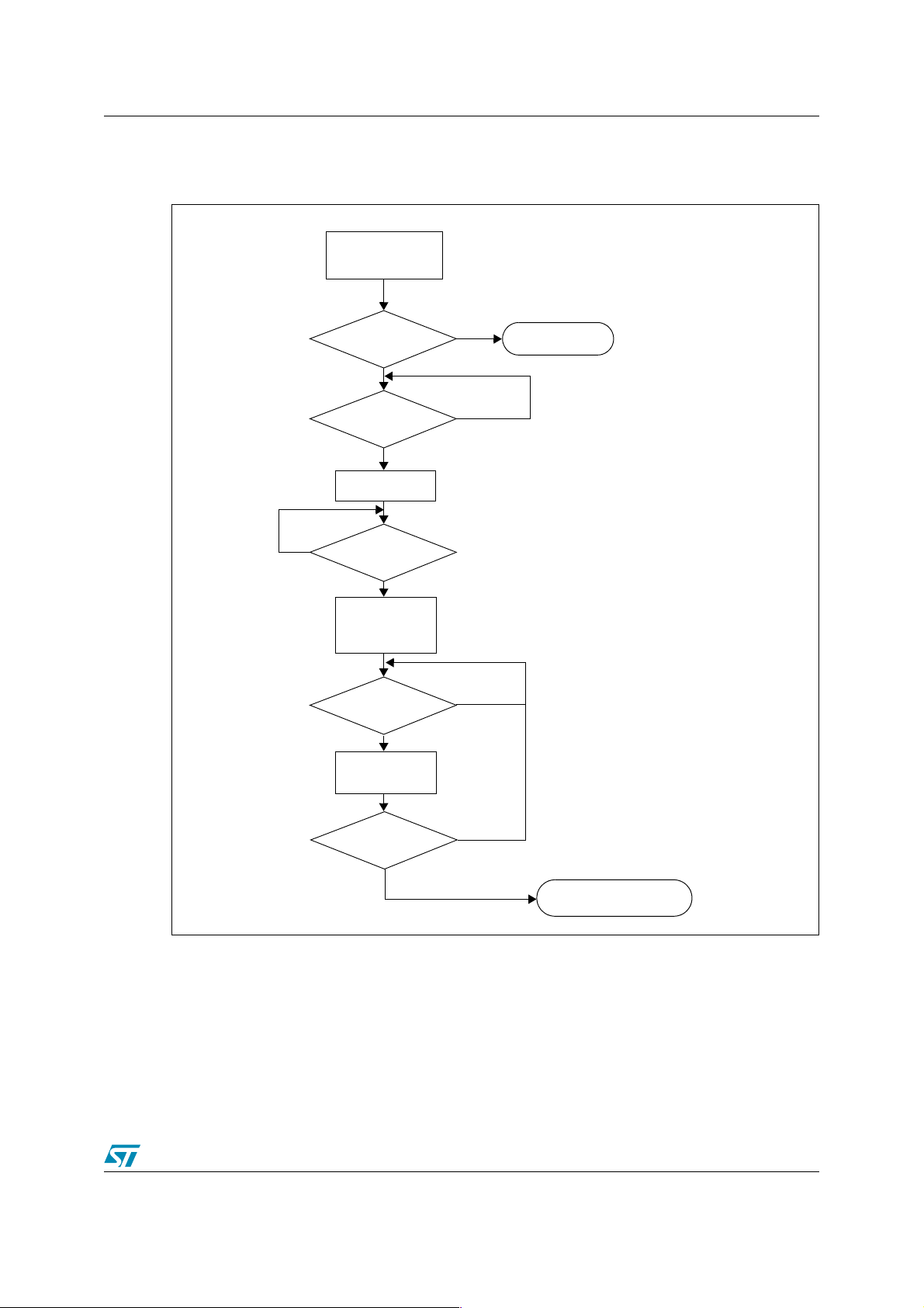
1.5 SystemMemory code program flow
Figure 1. SystemMemory code program flow
Start
Init PLL & IO ports
No
Debug Protection
Disabled ?
Falling Edge on
UART0 Rx ?
Start Timer Base 0
UART0 Rx == 1?
Stop Timer Base 0
Initialize UART0
Send Acknowledge
UART0 Byte
received?
Store Byte in RAM
Increment Address
No
No
EndLess Loop
No
All Bytes
received?
Done
No
Jump To Downloaded Code
at Address = 0xA0000000
Figure 1 shows the program flow of the SystemMemory code software. A few points worth
noting are:
● The boot process will not start if debug protection is active.
● The UART interface is only initialized if UART boot mode is detected.
Note: STR73x Timer Base 0 (TB0) is used to automatically detect the serial baud rate.
Once initialized the UART configuration is 8-bits, No Parity, and 1 Stop bit.
5/10
2 UART SystemMemory boot mode AN2260
2 UART SystemMemory boot mode
2.1 UART SystemMemory code sequence
After SystemMemory mode is entered and the STR73x is configured as described above, the
SystemMemory code begins to scan the RXD0 line, waiting to receive a zero byte (one start bit,
eight '0' data bits, and one stop bit).
The duration of this zero byte is measured using the Timer Base 0. The count value of the timer
is then used to calculate the corresponding baud rate factor with respect to the current system
clock.
Next, the code initializes the serial interface accordingly, and sets up pin TXD0 to an alternate
function, push-pull output. Using this calculated baud rate, an acknowledge byte is returned to
the host which signals that the STR73x is ready to receive the 128 bytes of download data.
Note: The watchdog timer is disabled during SystemMemory Mode, so the boot loading sequence is
not time limited.
Note: The acknowledge byte is 0x95 for the STR73x devices.
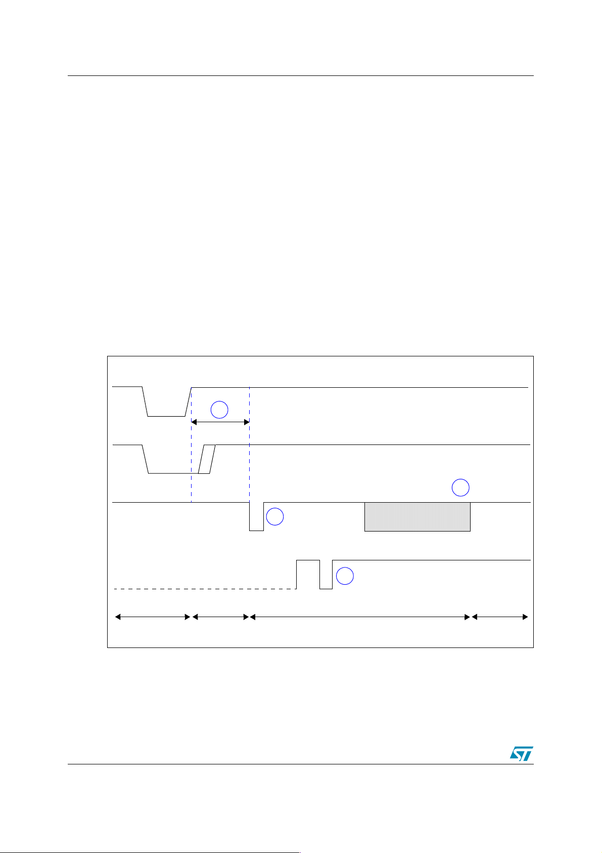
Figure 2. UART0 SystemMemory boot sequence
RSTIN
M1
RX
TX
Code
Reset
1
SysMemory
Code
2
3
SystemMemory UART branch
(1) Reset Stabilization & Code Initialization Time ( > 2ms)
(2) Zero Byte Reception
128 Byte transfer
4
Downloaded
Code
(3) Acknowledge Byte Transmission
(4) 128 Byte Loader Download
6/10
AN2260 2 UART SystemMemory boot mode
2.2 Choosing the UART baud rate
The calculation of the serial baud rate for UART0, from the length of the first zero byte that is
received, allows the operation of the STR73x SystemMemory boot loader within a wide range
of baud rates. However, the upper and lower limits have to be kept, in order to insure proper
data transfer.
STR73x Baud Rate = F
The STR73x uses Timer Base 0 to measure the length of the initial zero byte. The quantization
uncertainty of this measurement implies the first deviation from the theoretical baud rate. The
next deviation is implied by the computation of the UART0_BAUDRATE reload value from the
timer contents. The formula below shows the association:
TB0_CNT / 9 = 1 Bit Time in F
UART0_BAUDRATE = TB0_CNT / 9 / 16 = TB0_CNT / 144
For a correct data transfer from the host to the STR73x, the maximum deviation between the
internal initialized baud rate for UART0 and the real baud rate of the host should be below
2.5%. The deviation (f
, in percent) between the host baud rate and STR73x baud rate can be
B
calculated via the formula below:
f
= abs( (STR73x Baud Rate - Host Baud Rate) / STR73x Baud Rate) * 100%
B
<= 2.5%
f
B
/ 16 * UART0_BAUDRATE
cpu
(9 Bit Times the first ZERO Byte)
cpu
Note: Function (f
) does not consider the tolerances of oscillators and other devices supporting the
B
serial communication.
This baud rate deviation is a nonlinear function depending on the CPU clock and the baud rate
of the host. The maximum of the function (f
the smaller baud rate pre-scale factors, and the implied higher quantization error.
2.2.1 Minimum baud rate
B
is the minimum baud rate determined by the maximum count capacity of Timer Base 0
Low
when measuring the zero byte. This will be directly related to system clock frequency. Using the
maximum TB0_CNT value of 65535 in the equations above we end up with a minimum Baud
Rate of 1648 at F
Baud rates below B
= 12MHz. The lowest standard Baud Rate for this case would be 2400.
cpu
would cause TB0 to overflow. If this occurs, it would not be possible to
Low
properly initialize the UART0.
2.2.2 Maximum baud rate
B
is the highest baud rate in which the deviation still does not exceed the limit. All baud
High
rates between B
Low
and B
are below the deviation limit.
High
2.2.3 Higher baud rate deviations
A baud rate may be used as long as the actual deviation does not exceed the limit. Certain
lower baud rates may violate the deviation limit, while an even higher baud rate stays very well
below it. This relationship depends on the host interface.
) increases with the host baud rate. This is due to
B
7/10

3 Conclusion AN2260
3 Conclusion
The STR73x SystemMemory loader provides a convenient method for downloading user code
into on chip RAM for a variety of applications, such as programming of the embedded Flash.
The UART interface provides an easy and inexpensive, readily available serial link for desktop
users.
8/10

AN2260 4 Revision history
4 Revision history
Date Revision Changes
31-Oct-2005 1 First revision.
9/10
4 Revision history AN2260
“THE PRESENT NOTE WHICH IS FOR GUIDANCE ONLY AIMS AT PROVIDING CUSTOMERS WITH
INFORMATION REGARDING THEIR PRODUCTS IN ORDER FOR THEM TO SAVE TIME. AS A
RESULT, STMICROELECTRONICS SHALL NOT BE HELD LIABLE FOR ANY DIRECT, INDIRECT OR
CONSEQUENTIAL DAMAGES WITH RESPECT TO ANY CLAIMS ARISING FROM THE CONTENT OF
SUCH A NOTE AND/OR THE USE MADE BY CUSTOMERS OF THE INFORMATION CONTAINED
HEREIN IN CONNECTION WITH THEIR PRODUCTS.”
Information furnished is believed to be accurate and reliable. However, STMicroelectronics assumes no responsibility for the consequences
of use of such information nor for any infringement of patents or other rights of third parties which may result from its use. No license is granted
by implication or otherwise under any patent or patent rights of STMicroelectronics. Specifications mentioned in this publication are subject
to change without notice. This publication supersedes and replaces all information previously supplied. STMicroelectronics products are not
authorized for use as critical components in life support devices or systems without express written approval of STMicroelectronics.
The ST logo is a registered trademark of STMicroelectronics.
All other names are the property of their respective owners
© 2005 STMicroelectronics - All rights reserved
STMicroelectronics group of companies
Australia - Belgium - Brazil - Canada - China - Czech Republic - Finland - France - Germany - Hong Kong - India - Israel - Italy - Japan -
Malaysia - Malta - Morocco - Singapore - Spain - Sweden - Switzerland - United Kingdom - United States of America
www.st.com
10/10
 Loading...