

Page 1

AN2229
APPLICATION NOTE
Startup Behavior L9903/L9904
Introduction
Purpose of the Application Note is to detail the startup behaviour of L9903 and L9904 devices and to
explain a correct initialization sequence, possibly being necessary when application configuration is
different from the one suggested inside datasheet.
In fact, in case an additional, external diagnostic structure is used, it may happen that after a first
connection of the supply voltage, and before first enabling of the device, the measurement results of
these diagnostic structure is not precise.
AN2229/10-05 1/8
www.st.com
8
Page 2

AN2229
Contents
1 Explanation of 2 possible Startup Behaviors . . . . . . . . . . . . . . . . . . . . . . . 3
2 Application example using standby voltage monitoring . . . . . . . . . . . . . . 4
3 Proposed initialization sequences for L9903: . . . . . . . . . . . . . . . . . . . . . . . 5
4 Proposed initialization sequences L9904: . . . . . . . . . . . . . . . . . . . . . . . . . 6
5 Revision history . . . . . . . . . . . . . . . . . . . . . . . . . . . . . . . . . . . . . . . . . . . . . . . 7
2/8
Page 3
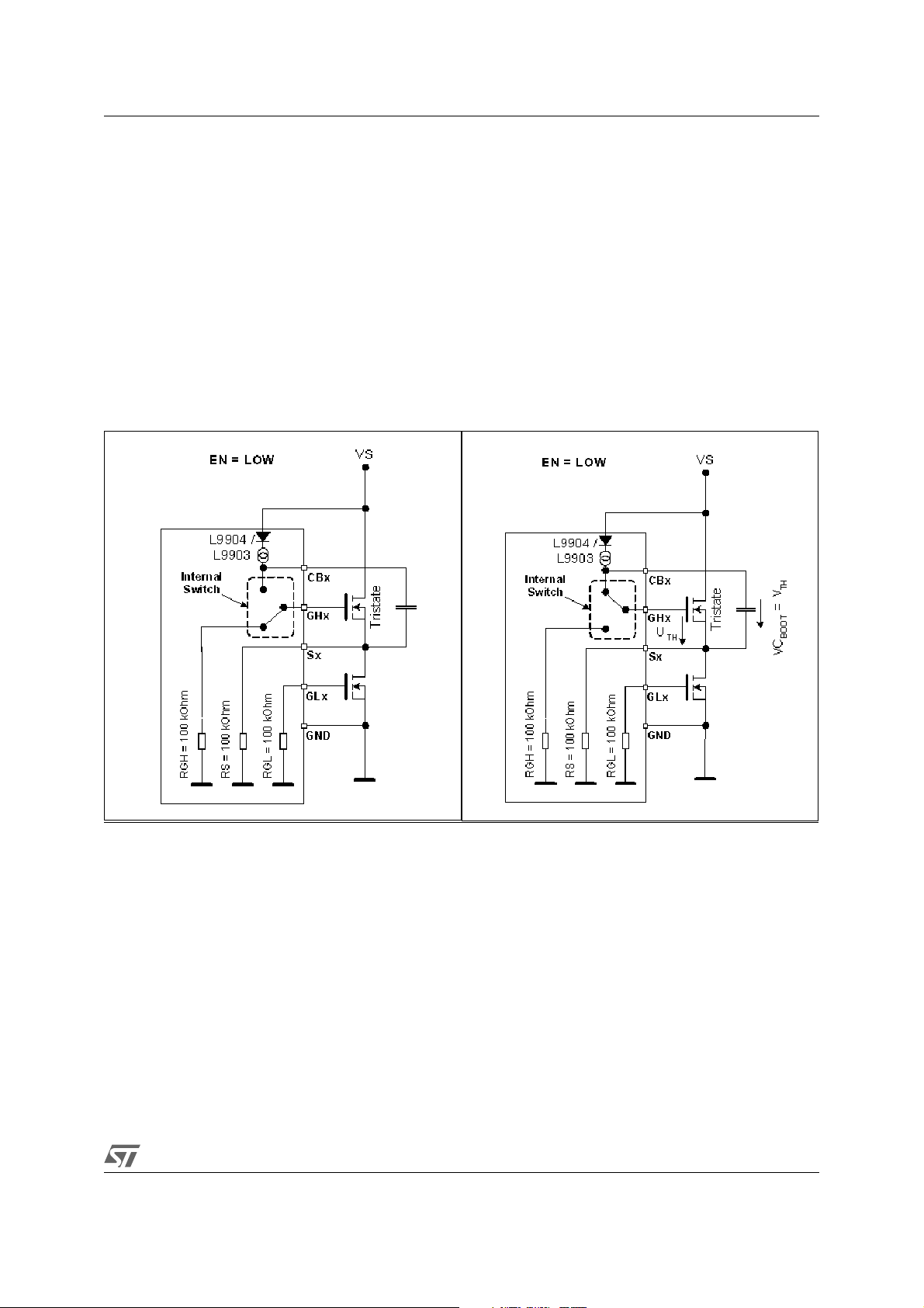
AN2229 1 Explanation of 2 possible Startup Behaviors
1 Explanation of 2 possible Startup Behaviors
Starting condition: the device is disconnected from the battery.
After switching on V
startup states:
a) Gate of high side driver is internally switched to ground (Fig. 1).
b) Gate of high side driver is internally switched to CBx (Fig. 2).
If the voltage (C
Figure 1. Startup behavior internal switched
to ground (state 1)
) exceeds 3.5V the device switches always like shown in figure 1
Boot
, as long as the voltage over C
S
is below 3.5V, the device can have 2
Boot
Figure 2. Startup behavior internal switch to
CBx (state 2.
After the first VS ramp up the outputs will enter one of the explained states.
If the device enters state 2 and the threshold of the external MOSFET is below 3.5V, the Sx pin will raise
and the charging of the bootstrap capacitor will be stopped. This state will persist until the L9903/04 will
be enabled by the EN pin. The only consequence of entering state 2 is an increased leakage current.
There is no influence on the standard application suggested inside datasheet. There is no influence on
operating condition (EN=HIGH). If the application requires a startup behavior like in figure 1, an
initialization is needed (see sections
3
and 4).
3/8
Page 4
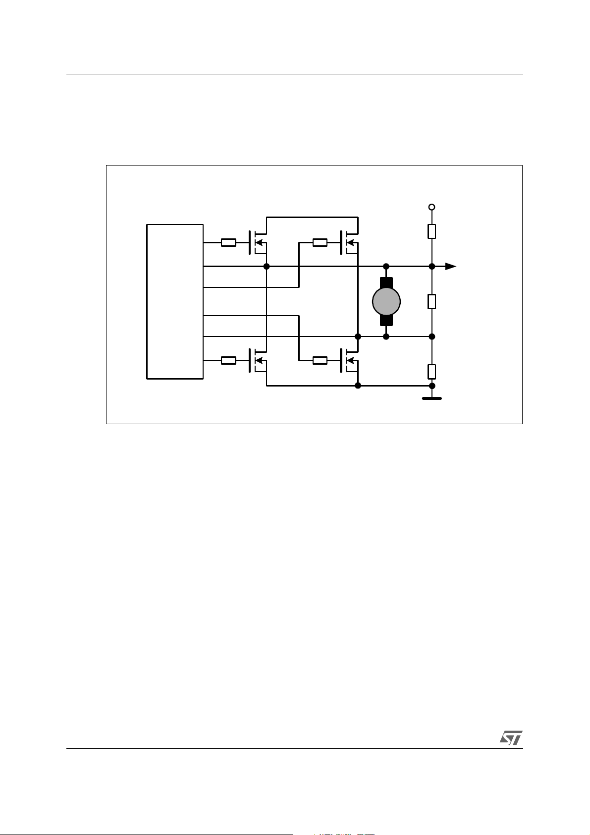
2 Application example using standby voltage monitoring AN2229
2 Application example using standby voltage
monitoring
Figure 3. DC motor driving with additional diagnostic (RD1, RD2, RD3)
Vcc
R
GH2
D1
R
R
ADC
D2
D3
S2
GH1
M
GL1
L9903/04
S1
GL2
Some applications may use external circuitry, for instance for advanced diagnosis in standby
mode. In figure 3 for example, an additional external resistive network is implemented, to
measure a potential short circuit or open load condition.
A short circuit or an open load condition can be detected by the ADC of a microcontroller, by
monitoring voltage levels of the resistive network.
If L9903/04 is not initialized correctly upon first V
entered. The voltage levels of the external circuitry could be influenced, eventually leading to a
temporary wrong diagnosis.
Hence it is mandatory to initialize the device if the application requires monitoring of voltage
levels in standby mode (EN=LOW) after the first V
not influenced. Later standby modes are also not influenced.
ramp up, the described state 2 could be
S
ramp up. Normal operation (EN=HIGH) is
S
Once the device is initialized properly, the resistive output versus ground is always present
(figure 1) in standby mode.
4/8
Page 5
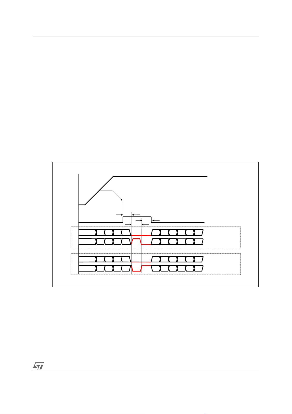
AN2229 3 Proposed initialization sequences for L9903:
3 Proposed initialization sequences for L9903:
Alternative 1: Vs > 7V
EN = High for >50
PWM = Low after 50
DIR = High for >10
DIR = Low for >10
Alternative 2: Vs > 7V
EN = High after 50
PWM = Low positive Edge after min 50
DIR = Low for >10
DIR = High for >10
Figure 4. Proposed Sequence to Initialize L9903 after VS is applied
VS
EN
PWM
DIR
µs
µs of EN
µs after min 50µs of EN
µs after min 10µs DIR = High after min 50µs of EN
µs of EN
µs of EN
µs after min 50µs of EN
µs after min 10µs DIR = Low after min 50µs of EN
VS should be >7V before EN=HI
>50us
>10us
>10us
Alternative 1:
pos. Pulse at DIR
with PWM=0
PWM
DIR
Alternative 2:
neg. Pulse at DIR
with PWM=0
Two possible solutions. Important is that after enabling the L9903 both LS transistors willb be switched-on
(Sx forced o GND) for at least 10
realized by changing the DIR-input while PWM is low. The min 50
circuit to setup. A signal change within the 50
µs (C
=100nF) to allow boostrap capacitor to be charged. This is
boot
µs delay are needed for the internal
µs may not be detected.
5/8
Page 6
4 Proposed initialization sequences L9904: AN2229
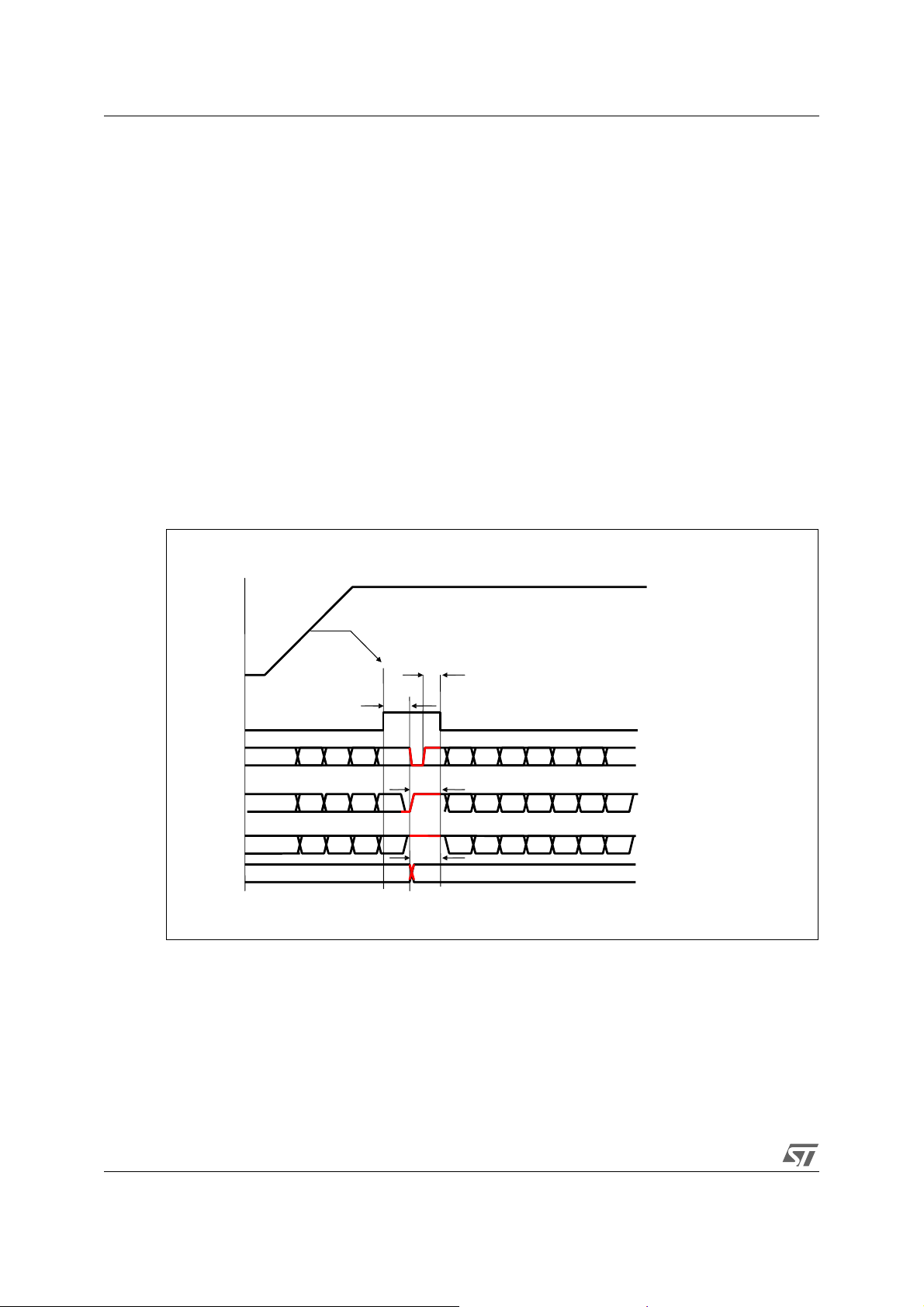
4 Proposed initialization sequences L9904:
Alternative 1: Vs > 7V
EN = High for >50
PWM = Low Pulse after 50
PWM = 1 for >10
Alternative 2: Vs > 7V
EN = High for >50
PWM = Edge positive Edge after min 50
PWM = 1 for >10
Alternative 3: Vs > 7V
EN = High for >50
PWM = 1 for >10
DIR=Edge after 50
Figure 5. Proposed Sequence to Initialize L9904 after VS is applied
VS
EN
µs
µs of EN
µs
µs
µs
µs
µs after Edge of DIR 50µs of EN
µs of EN
VS should be >7V before EN=HI
>10us
>50us
EN
µs of EN
PWM
PWM
PWM
DIR
>10us
>10us
Alternativ 1:
Pulse at PWM
Alternative 2:
pos. Edge PWM
Alternative 3:
Edge at DIR
with PWM=1
Three possible solutions. Important is that PWM=1 will be detected after enabling the L9904 to switch on
both LS transistors (break mode). Therefore an edge at PWM or DIR input has to be present 50
more) after EN was set HI. The 50
within the 50
µs may not be detected. After this edge the PWM should be HI for at least 10µs (C
µs delay are needed for the internal circuit to setup. A signal change
µs (or
Boot
100nF) to charge the CBx bootsstrap capacitors (depending on value of capacitor)
6/8
=
Page 7
AN2229
5 Revision history
Date Revision Changes
October 2005 1 Initial release.
7/8
Page 8

5 Revision history AN2229
Information furnished is believed to be accurate and reliable. However, STMicroelectronics assumes no responsibility for the consequences
of use of such information nor for any infringement of patents or other rights of third parties which may result from its use. No license is granted
by implication or otherwise under any patent or patent rights of STMicroelectronics. Specifications mentioned in this publication are subject
to change without notice. This publication supersedes and replaces all information previously supplied. STMicroelectronics products are not
authorized for use as critical components in life support devices or systems without express written approval of STMicroelectronics.
The ST logo is a registered trademark of STMicroelectronics.
All other names are the property of their respective owners
© 2005 STMicroelectronics - All rights reserved
STMicroelectronics group of companies
Australia - Belgium - Brazil - Canada - China - Czech Republic - Finland - France - Germany - Hong Kong - India - Israel - Italy - Japan -
Malaysia - Malta - Morocco - Singapore - Spain - Sweden - Switzerland - United Kingdom - United States of America
www.st.com
8/8
 Loading...