

查询74V2T384供应商
74V2T384
DUAL HIGH SPEED BUS SWITCH
■ HIGH SPEED: t
■ COMPATIBLE WITH TTL LEVEL
■ LOW POWER DISSIPATION:
I
=1µA(MAX.) atTA=25°C
CC
■ LOW "ON" RESISTANCE at V
R
=7Ω (TYP.) VIN=0VI
ON
R
=20Ω (TYP.) VIN=2.4VI
ON
■ OPERATING VOLTAGE RANGE:
V
(OPR) = 4.0V TO 5.5V
CC
■ 5V TOLERANT ON CONTROL PIN
■ IMPROVED LATCH-UP IMMUNITY
= 0.5ns (TYP.) at VCC=5V
PD
=5.0V:
CC
= 30mA
I/O
= 10mA
I/O
DESCRIPTION
The 74V2T384 is an advanced high-speed CMOS
DUAL HIGH SPEED BUS SWITCH fabricated in
silicon gate C
2
MOS technology. It’s designed to
operate from 4.5V to 5.5V, m aking this device
ideal for portable applications. It’s offers 7Ω
Resistance typical value at V
key feature are fast switching speed (t
=4.5V. Additional
CC
=3.8ns,
ON
SOT23-8L
ORDER CODES
PACKAGE T & R
SOT23-8L 74V2T384STR
t
=3.3ns Typical) and Low Power
OFF
Consumption.
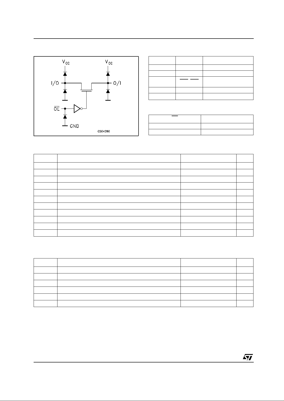
TheOE
switch is ON when the OE
OFF when OE
input is provided to control the s w itch; the
input is held low and
is held high.
It’s available in the c ommercial and extended
temperature range in SOT23-8L pa ckage.
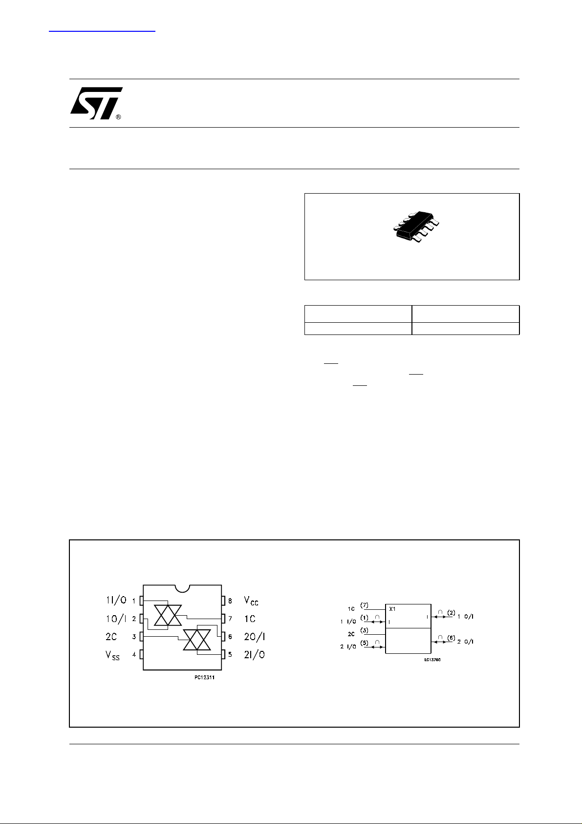
PIN CONNECTION AND IEC LOGIC SYMBOLS
1/7June 2003
74V2T384
INPUT EQUIVALENT CIRCUIT PIN DESCRIPTION
PIN No SYMBOL NAME AND FUNCTION
1, 5 1I/O, 2I/O Independent Input/Output
2, 6 1O/I, 2O/I Independent Output/Input
7, 3 1OE
4 GND Ground (0V)
8
TRUTH TABLE
V
, 2OE
CC
Enable Input (Active
HIGH)
Positive Supply Voltage
OE
SWITCH FUNCTION
LON
H OFF *
* High Impedance State
ABSOLUTE MAXIMUM RATINGS
Symbol Parameter Value Unit
V
V
V
V
I
I
I
OK
I
or I
I
CC
T
T
Absolute Maximum Ratings are those values beyond which damage to the device may occur. Functional operation under these conditions is
not implied
Supply Voltage
CC
DC Input Voltage -0.5 to VCC+ 0.5
I
DC Control Input Voltage
IC
DC Output Voltage -0.5 to VCC+ 0.5
O
DC Input Diode Current
IK
DC Control Input Diode Current
IK
DC Output Diode Current
DC Output Current
O
DC VCCor Ground Current
GND
Storage Temperature
stg
Lead Temperature (10 sec)
L
-0.5 to +7.0 V
V
-0.5 to +7.0 V
V
± 20 mA
-20 mA
± 20 mA
± 50 mA
± 50 mA
-65 to +150 °C
300 °C
RECOMMENDED OPERATING CONDITIONS
Symbol Parameter Value Unit
V
V
V
V
T
dt/dv
1) VINfrom0.8V to 2Von control pin
Supply Voltage
CC
Input Voltage 0 to V
I
Control Input Voltage
IC
Output Voltage 0 to V
O
Operating Temperature
op
Input Rise and Fall Time (note 1) V
CC
= 5.0V
4.0 to 5.5 V
CC
0 to 5.5 V
CC
-55 to 125 °C
0 to 20 ns/V
2/7
V
V

DC SPECIFICATIONS
Symbol Parameter
V
V
R
R
I
∆I
High Level Input
IH
Voltage
V
Low Level Input
IL
Voltage
High Level Input
IH
Voltage
Low Level Input
V
IL
Voltage
ON Resistance
ON
ON Resistance
ON
Input/Output
OFF
Leakage Current
(SWITCH OFF)
Control Input
I
IN
Leakage Current
Quiescent Supply
I
CC
Current
Increase Quiescent
CC
Supply Current per
Control Input
74V2T384
Test Condition Value
= 25°C
T
V
(V)
5.0
5.0
CC
(*)
(*)
A
Min. Typ. Max. Min. Max. Min. Max.
222V
4.0 2 2 2 V
4.0 0.8 0.8 0.8 V
4.5
4.5
VIC=V
V
I/O
I
≤ 30mA
I/O
VIC=V
V
I/O
I
≤ 10mA
I/O
IL
=GND
IL
= 2.4V
71015V
20 40 60 V
5.5 VOS=VCCto GND
V
IS=VCC
0to
VIC= 5.5V or GND
5.5
V
5.5
I=VCC
V
other V
5.5
V
IC=VIH
IC=VCC
IC=VCC
to GND
or GND
-2.1V
or
GND
-40 to 85°C -55 to 125°C
0.8 0.8 0.8 V
±0.1 ± 1 ± 10 µA
± 0.1 ± 1.0 ± 1.0 µA
11020µA
1.35 2.5 3.5 mA
Unit
AC ELECTRICAL CHARACTERISTICS (C
Test Condition Value
Symbol Parameter
t
t
PLZ
t
PHZ
t
PZL
t
PZH
(*) Voltage range is5.0V ± 0.5V
PD
Delay Time
Output Disable
Time
Output Enable
Time
V
(V)
5.0
5.0
5.0
CC
(*)
(*)
(*)
tr=tr=6ns
RL=500Ω
VIN= 2.4V
RL=1KΩ
VIN= 2.4V
= 50pF, Input tr=tf= 3ns)
L
= 25°C
T
A
Min. Typ. Max. Min. Max. Min. Max.
0.5 0.8 1.0 1.5 ns
3.8 6.5 9.0 10.0 ns
3.3 5.0 7.5 8.5 ns
-40 to 85°C -55 to 125°C
Unit
3/7

74V2T384
CAPACITIVE CH ARACTERISTICS
Test Condition Value
= 25°C
Symbol Parameter
T
A
Min. Typ. Max. Min. Max. Min. Max.
C
C
C
Input Capacitance
IN
Output
I/O
Capacitance
Power Dissipation
PD
Capacitance
410 10 10pF
7pF
3pF
(note 1)
1) CPDis defined as the value of the IC’s internal equivalent capacitance which is calculated from the operating current consumption without
load. (Refer to Test Circuit). Average operating currentcanbeobtained by the following equation. I
-40 to 85°C -55 to 125°C
CC(opr)=CPDxVCCxfIN+ICC
Unit
/2(per switch)
4/7

74V2T384
SOT23-8L MECHANICAL DATA
mm. mils
DIM.
MIN. TYP MAX. MIN. TYP. MAX.
A 0.90 1.45 35.4 57.1
A1 0.00 0.15 0.0 5.9
A2 0.90 1.30 35.4 51.2
b 0.22 0.38 8.6 14.9
C 0.09 0.20 3.5 7.8
D 2.80 3.00 110.2 118.1
E 2.60 3.00 102.3 118.1
E1 1.50 1.75 59.0 68.8
e0.65 25.6
e1 1.95 76.7
L 0.35 0.55 13.7 21.6
5/7

74V2T384
Tape & Reel SOT23-xL MECHANICAL DATA
DIM.
MIN. TYP MAX. MIN. TYP. MAX.
A 180 7.086
C 12.8 13.0 13.2 0.504 0.512 0.519
D 20.2 0.795
N 60 2.362
T 14.4 0.567
Ao 3.13 3.23 3.33 0.123 0.127 0.131
Bo 3.07 3.17 3.27 0.120 0.124 0.128
Ko 1.27 1.37 1.47 0.050 0.054 0.0.58
Po 3.9 4.0 4.1 0.153 0.157 0.161
P 3.9 4.0 4.1 0.153 0.157 0.161
mm. inch
6/7

74V2T384
Information furnished is believed to be accurate and reliable. However, STMicroelectronics assumes no responsibility for the
consequences of use o f suc h inf ormat ion n or f or an y infr ingeme nt of paten ts or oth er ri gh ts of third part ies whic h may resul t f rom
its use. No license is granted by implication or otherwise under any patent or patent rights of STMicroelectronics. Specifications
mentioned in this publication are subject to change without notice. This publication supersedes and replaces all information
previously supplied. STMicroelectronics products are not authorized for use as critical components in life support devices or
systems without express written approval of STMicroelectronics.
Australia - Brazil - Canada - China - Finland - France - Germany - Hong Kong - India - Israel - Italy - Japan - Malaysia - Malta - Morocco
© The ST logo is a registered trademark of STMicroelectronics
© 2003 STMicroelectronics - Printed in Italy - All Rights Reserved
STMicroelectronics GROUP OF COMPANIES
Singapore - Spain - Sweden - Switzerland - United Kingdom - United States.
© http://www.st.com
7/7

WWW.ALLDATASHEET.COM
Copyright © Each Manufacturing Company.
All Datasheets cannot be modified without permission.
This datasheet has been download from :
www.AllDataSheet.com
100% Free DataSheet Search Site.
Free Download.
No Register.
Fast Search System.
www.AllDataSheet.com
 Loading...