

Features
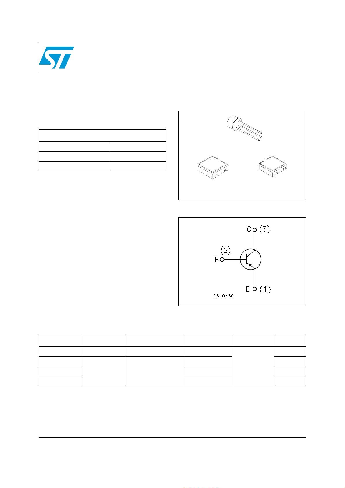
TO-18
LCC-3
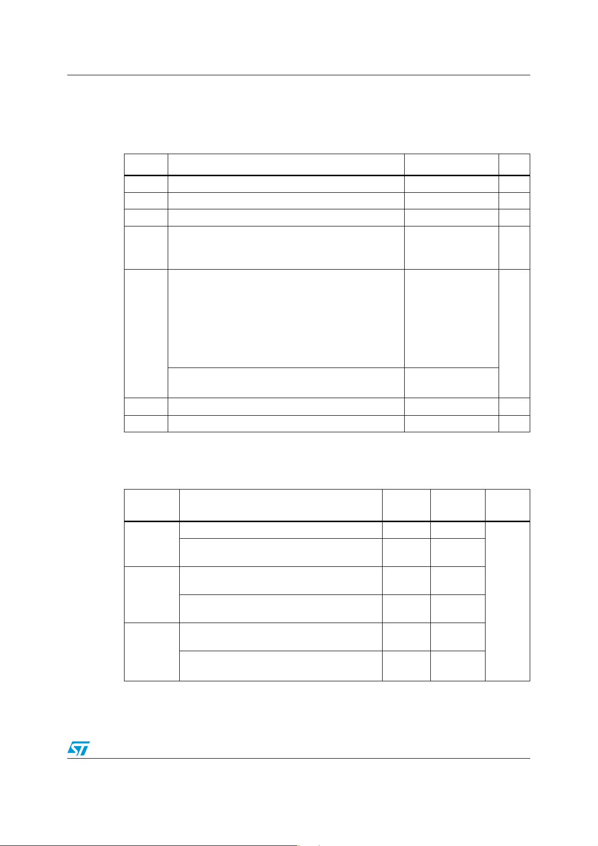
3
1
2
3
1
2
LCC-3UB
Pin 4 in LCC-3UB is connected to the metallic lid.
Parameter Value
2N2907AHR
Hi-Rel 60 V - 0.6 A PNP transistor
Datasheet — production data
BV
CEO
(max) 0.6 A
I
C
H
at 10 V - 150 mA > 100
FE
■ Linear gain characteristics
■ Hermetic packages
■ ESCC and JANS qualified
■ European preferred part list EPPL
60 V
Description
The 2N2907AHR is a silicon planar PNP
transistor specifically designed and housed in
hermetic packages for aerospace and Hi-Rel
applications. It is available in the JAN qualification
system (MIL-PRF19500 compliance) and in the
ESCC qualification system (ESCC 5000
compliance). In case of discrepancies between
this datasheet and the relevant agency
specification, the latter takes precedence.
3
4
1
2
Figure 1. Internal schematic diagram
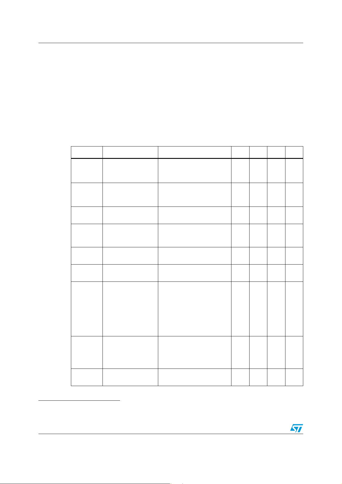
Table 1. Device summary
Order codes Qualification Agency spec. Package Radiation level EPPL
JANS2N2907A JANS MIL-PRF-19500/291 LCC-3UB
2N2907AUB
SOC2907A LCC-3 Yes
2N2907AHR TO-18 -
1. Contact ST sales office for information about the specific conditions for products in die form and other JAN quality levels.
May 2012 Doc ID 15382 Rev 3 1/16
This is information on a product in full production.
ESCC 5201/001
(1)
-
LCC-3UB Yes
-
www.st.com
16

Contents 2N2907AHR
Contents
1 Electrical ratings . . . . . . . . . . . . . . . . . . . . . . . . . . . . . . . . . . . . . . . . . . . . 3
2 Electrical characteristics . . . . . . . . . . . . . . . . . . . . . . . . . . . . . . . . . . . . . 4
2.1 JANS electrical characteristics . . . . . . . . . . . . . . . . . . . . . . . . . . . . . . . . . . 4
2.2 ESCC electrical characteristics . . . . . . . . . . . . . . . . . . . . . . . . . . . . . . . . . 5
2.3 Electrical characteristics (curves) . . . . . . . . . . . . . . . . . . . . . . . . . . . . . . . . 6
2.4 Test circuits . . . . . . . . . . . . . . . . . . . . . . . . . . . . . . . . . . . . . . . . . . . . . . . . . 7
3 Package mechanical data . . . . . . . . . . . . . . . . . . . . . . . . . . . . . . . . . . . . . 9
4 Order codes . . . . . . . . . . . . . . . . . . . . . . . . . . . . . . . . . . . . . . . . . . . . . . . 14
5 Shipping details . . . . . . . . . . . . . . . . . . . . . . . . . . . . . . . . . . . . . . . . . . . . 14
5.1 Data code . . . . . . . . . . . . . . . . . . . . . . . . . . . . . . . . . . . . . . . . . . . . . . . . . 14
5.2 Documentation . . . . . . . . . . . . . . . . . . . . . . . . . . . . . . . . . . . . . . . . . . . . . 15
6 Revision history . . . . . . . . . . . . . . . . . . . . . . . . . . . . . . . . . . . . . . . . . . . 16
2/16 Doc ID 15382 Rev 3
2N2907AHR Electrical ratings
1 Electrical ratings
Table 2. Absolute maximum ratings
Symbol Parameter Value Unit
V
V
V
Collector-base voltage (IE = 0) -60 V
CBO
Collector-emitter voltage (IB = 0) -60 V
CEO
Emitter-base voltage (IC = 0) -5 V
EBO
Collector current
I
for TO-18
C
for LCC-3 and LCC-3UB
Total dissipation at T
amb
≤ 25 °C
ESCC: TO-18
LCC-3 and LCC-3UB
LCC-3 and LCC-3UB
P
JANS: LCC-3UB
TOT
Total dissipation at T
case
≤ 25 °C
(1)
ESCC: TO-18
Total dissipation at T
sp(IS)
= 25 °C
JANS: LCC-3UB
T
1. When mounted on a 15 x 15 x 0.6 mm ceramic substrate.
Storage temperature -65 to 200 °C
stg
T
Max. operating junction temperature 200 °C
J
-0.6
-0.5
0.4
0.4
0.73
0.5
1.8
1
A
A
W
Table 3. Thermal data
Symbol Parameter
Thermal resistance junction-case (max) for JANS - -
R
thJC
Rt
hJSP(IS)
R
thJA
1. When mounted on a 15 x 15 x 0.6 mm ceramic substrate.
Thermal resistance junction-case (max) for
ESCC
Thermal resistance junction-solder pad (infinite
sink) (max) for JANS
Thermal resistance junction-solder pad (infinite
sink) (max) for ESCC
Thermal resistance junction-ambient (max) for
JANS
Thermal resistance junction-ambient (max) for
ESCC
Doc ID 15382 Rev 3 3/16
LCC-3
LCC-3UB
TO-18 Unit
-97
90 -
--
325 -
437
240
(1)
437
°C/W
Electrical characteristics 2N2907AHR
2 Electrical characteristics
(a)
JANS and ESCC version of the products are assembled and tested in compliance with the
agency specification it is qualified in. The electrical characteristics of each version are
provided in dedicated tables.
T
= 25 °C unless otherwise specified.
case
2.1 JANS electrical characteristics
Table 4. JANS electrical characteristics
Symbol Parameter Test conditions Min. Typ. Max. Unit
= 60 V
V
CB
V
= 50 V
CB
VCB= 50 V T
= 50 V - 50 nA
V
CE
= 5 V
V
EB
V
= 4 V
EB
= 10 mA 60 - V
I
C
= 150 mA IB = 15 mA
I
C
IC = 500 mA IB = 50 mA
I
CBO
I
CES
I
EBO
V
(BR)CEO
V
CE(sat)
Collector cut-off
current (I
= 0)
E
Collector cut-off
current
(I
= 0)
E
Emitter cut-off current
(I
= 0)
C
Collector-emitter
(1)
breakdown voltage
= 0)
(I
B
Collector-emitter
(1)
saturation voltage
= 150 °C
amb
10
-
10
10
10
50
0.4
-
1.6
µA
nA
µA
µA
nA
V
V
= 150 mA IB = 15 mA
V
BE(sat)
Base-emitter
(1)
saturation voltage
I
C
IC=500mA IB =50mA
= 0.1 mA V
I
C
IC = 1 mA V
I
= 10 mA V
(1)
h
FE
DC current gain
C
= 150 mA V
I
C
IC = 500 mA V
I
= 10 mA V
C
T
= -55 °C
amb
= 20 V IC = 20 mA
V
CE
h
fe
Small signal current
gain
f = 100 MHz
V
= 10 V IC =1 mA
CE
f = 1 kHz
C
obo
a. For PNP type, voltage and current values are negative.
Output capacitance
(I
= 0)
E
= 10 V
V
CB
100 kHz ≤ f ≤ 1 MHz
4/16 Doc ID 15382 Rev 3
CE
CE
CE
CE
CE
CE
= 10 V
= 10 V
= 10 V
= 10 V
= 10 V
= 10 V
0.6 1.3
2.6
75
100
450
100
100
-
300
50
50
2
100
-
-8pF
V
2N2907AHR Electrical characteristics
Table 4. JANS electrical characteristics (continued)
Symbol Parameter Test conditions Min. Typ. Max. Unit
C
ibo
t
on
t
off
1. Pulsed duration = 300 µs, duty cycle ≤ 2 %
Output capacitance
(IE = 0)
Tu r n - on t i m e
Turn-off time
V
= 2 V
EB
100 kHz ≤ f ≤ 1 MHz
V
= 30 V IC = 150 mA
CC
I
= 15 mA
B1
V
= 30 V IC = 150 mA
CC
I
= -I
B1
= 15 mA
B2
2.2 ESCC electrical characteristics
Table 5. ESCC electrical characteristics
Symbol Parameter Test conditions Min. Typ. Max. Unit
= 50 V
I
CBO
V
(BR)CBO
V
(BR)CEO
V
(BR)EBO
V
CE(sat)
Collector cut-off
current (I
Collector-base
breakdown voltage
= 0)
(I
E
Collector-emitter
(1)
breakdown voltage
= 0)
(I
B
Emitter-base
breakdown voltage
(I
= 0)
C
Collector-emitter
(1)
saturation voltage
= 0)
E
V
CB
V
= 50 V T
CB
= 10 µA 60 - V
I
C
= 10 mA 60 - V
I
C
= 10 µA 5 - V
I
E
= 150 mA IB = 15 mA - 0.4 V
I
C
= 150 °C
amb
-30pF
-45ns
- 300 ns
10
10
nA
µA
V
BE(sat)
(1)
saturation voltage
I
C
Base-emitter
IC = 0.1 mA V
(1)
h
FE
h
fe
C
obo
t
on
t
off
1. Pulsed duration = 300 µs, duty cycle ≤ 2 %
DC current gain
Small signal current
gain
Output capacitance
(IE = 0)
Tu r n - on t i m e
Turn-off time
IC = 10 mA V
I
C
I
C
V
f = 100 MHz
V
100 kHz ≤ f ≤ 1 MHz
V
I
B1
V
I
B1
Doc ID 15382 Rev 3 5/16
= 150 mA IB = 15 mA 0.87 1.3 V
= 10 V
CE
= 10 V
CE
= 150 mA V
= 500 mA V
= 20 V IC = 20 mA
CE
= 10 V
CB
= 30 V IC = 150 mA
CC
CE
CE
= 10 V
= 10 V
= 15 mA
= 30 V IC = 150 mA
CC
= -I
= 15 mA
B2
75
100
100
-
50
2-
-8pF
-45ns
- 300 ns
300

Electrical characteristics 2N2907AHR
!-V
!-V
!-V
!-V
2.3 Electrical characteristics (curves)
Figure 2. DC current gain (V
=1 V) Figure 3. DC current gain (VCE=10 V)
CE
Figure 4. Collector emitter saturation
voltage
Figure 5. Base emitter saturation
voltage (h
FE
=10)
6/16 Doc ID 15382 Rev 3

2N2907AHR Electrical characteristics
NOTES:
1. The rise time (t
r
) of the applied pulse shall be ≤ 2.0 ns, duty cycle ≤ 2 percent and the generator
source impedance shall be 50 ohms.
2. Sampling oscilloscope: Z
in
≥ 100 K ohms, Cin≤ 12 pF, rise time ≤ 5 ns.
NOTES:
1. The rise time (t
r
) of the applied pulse shall be ≤ 2.0 ns, duty cycle ≤ 2 percent and the generator
source impedance shall be 50 ohms.
2. Sampling oscilloscope: Z
in
≥ 100 K ohms, Cin≤ 12 pF, rise time ≤ 5 ns.
2.4 Test circuits
Figure 6. JANS saturated turn-on switching time test circuit
Figure 7. JANS saturated turn-off switching time test circuit
Doc ID 15382 Rev 3 7/16

Electrical characteristics 2N2907AHR
Figure 8. ESCC resistive load switching test circuit
1. Fast electronic switch
2. Non-inductive resistor
8/16 Doc ID 15382 Rev 3

2N2907AHR Package mechanical data
3 Package mechanical data
In order to meet environmental requirements, ST offers these devices in different grades of
®
ECOPACK
specifications, grade definitions and product status are available at: www.st.com.
ECOPACK
packages, depending on their level of environmental compliance. ECOPACK®
®
is an ST trademark.
Table 6. Product mass summary
Package Mass (g)
LCC-3UB 0.06
LCC-3 0.06
TO-18 0.40
Doc ID 15382 Rev 3 9/16

Package mechanical data 2N2907AHR
Table 7. LCC-3UB mechanical data
mm.
Dim.
Min. Typ. Max.
A 1.16 1.42
C 0.46 0.51 0.56
D 0.56 0.76 0.96
E 0.92 1.02 1.12
F 1.95 2.03 2.11
G 2.92 3.05 3.18
I 2.41 2.54 2.67
J 0.42 0.57 0.72
K 1.37 1.52 1.67
L 0.41 0.51 0.61
M 2.46 2.54 2.62
N 1.81 1.91 2.01
r 0.20
r1 0.30
r2 0.56
Figure 9. LCC-3UB drawings
10/16 Doc ID 15382 Rev 3

2N2907AHR Package mechanical data
Table 8. LCC-3 mechanical data
mm.
Dim.
Min. Typ. Max.
A 1.16 1.42
C 0.45 0.50 0.56
D 0.60 0.76 0.91
E 0.91 1.01 1.12
F 1.95 2.03 2.11
G 2.92 3.05 3.17
I 2.41 2.54 2.66
J 0.42 0.57 0.72
K 1.37 1.52 1.67
L 0.40 0.50 0.60
M 2.46 2.54 2.62
N 1.80 1.90 2.00
R 0.30
Figure 10. LCC-3 drawings
2
3
1
Doc ID 15382 Rev 3 11/16

Package mechanical data 2N2907AHR
Table 9. TO-18 mechanical data
mm.
Dim.
Min. Typ. Max.
A 12.7
B 0.49
D 5.3
E 4.9
F 5.8
G 2.54
H 1.2
I 1.16
L 45°
Figure 11. TO-18 drawings
12/16 Doc ID 15382 Rev 3

13/16 Doc ID 15382 Rev 3
4 Order codes
Order codes 2N2907AHR
Table 10. Order codes
Part number Agency specification EPPL Quality level
J2N2907AUB1
2N2907AUB1 -
SOC2907A -
JANS2N2907AUBG MIL-PRF-19500/291 -
JANS2N2907AUBT MIL-PRF-19500/291 - LCC-3UB Solder Dip JS2907 Waffle pack
2N2907AUB06 5202/001/06 Yes
Radiation
level
-
-
Engineering model
JANS
Engineering model
ESCC
Engineering model
ESCC
Package Lead Finish Marking
LCC-3UB Gold J2N2907A Waffle pack
LCC-3UB Gold U03 Waffle pack
LCC-3 Gold P03 Waffle pack
(1)
Packing
LCC-3UB Gold JS2907 Waffle pack
JANS flight
-
LCC-3UB Gold 520200106 Waffle pack
2N2907AUB07 5202/001/07 Yes LCC-3UB Solder Dip 520200107 Waffle pack
SOC2907AHRB 5202/001/04 or 05
2N2907AHR 5202/001/01 or 02
1. Specific marking only. The full marking includes in addition:
For the engineering models : ST logo, date code, country of origin (FR).
For ESCC flight parts : ST logo, date code, country of origin (FR), ESA logo, serial number of the part within the assembly lot.
For JANS flight parts : ST logo, date code, country of origin (FR), manufacturer code (CSTM), serial number of the part within the assembly lot.
2. Depending ESCC part number mentioned on the purchase order.
(2)
(2)
Yes LCC-3
-TO-18
ESCC flight
Gold or
Solder Dip
Gold or
Solder Dip
(2)
(2)
520200104
(2)
or 05
520200101
(2)
or 02
Waffle pack
Strip pack
Contact ST sales office for information about the specific conditions for:
– Products in die form
– Other JANS quality levels
– Tape and reel packing

Shipping details 2N2907AHR
5 Shipping details
5.1 Data code
Data code is structured as described below:
– EM (ESCC and JANS) xyywwz
– ESCC Flight yywwz
– JANS Flight xyywwz
where:
xyywwz
3: EM
W: flight part/ diffused
in
Singapore
Last two digits year
Week digits
Lot index in the week
5.2 Documentation
Table 11. Documentation provided for each type of product
Quality level Radiation level Documentation
Engineering model - -
JANS Flight - Certificate of conformance
ESCC Flight - Certificate of conformance
14/16 Doc ID 15382 Rev 3

2N2907AHR Revision history
6 Revision history
Table 12. Document revision history
Date Revision Changes
09-Feb-2009 1 Initial release
– Modified Table 1 on page 1
30-Nov-2011 2
14-May-2012 3
– Minor text changes in the document title and description on the
coverpage
New package inserted (LCC-3UB).
Updated:
– Table 1: Device summary, Table 2: Absolute maximum ratings and
Table 3: Thermal data.
– Section 2: Electrical characteristics and Section 3: Package
mechanical data.
Added:
– Section 4: Order codes and Section 5: Shipping details.
Doc ID 15382 Rev 3 15/16

2N2907AHR
Please Read Carefully:
Information in this document is provided solely in connection with ST products. STMicroelectronics NV and its subsidiaries (“ST”) reserve the
right to make changes, corrections, modifications or improvements, to this document, and the products and services described herein at any
time, without notice.
All ST products are sold pursuant to ST’s terms and conditions of sale.
Purchasers are solely responsible for the choice, selection and use of the ST products and services described herein, and ST assumes no
liability whatsoever relating to the choice, selection or use of the ST products and services described herein.
No license, express or implied, by estoppel or otherwise, to any intellectual property rights is granted under this document. If any part of this
document refers to any third party products or services it shall not be deemed a license grant by ST for the use of such third party products
or services, or any intellectual property contained therein or considered as a warranty covering the use in any manner whatsoever of such
third party products or services or any intellectual property contained therein.
UNLESS OTHERWISE SET FORTH IN ST’S TERMS AND CONDITIONS OF SALE ST DISCLAIMS ANY EXPRESS OR IMPLIED
WARRANTY WITH RESPECT TO THE USE AND/OR SALE OF ST PRODUCTS INCLUDING WITHOUT LIMITATION IMPLIED
WARRANTIES OF MERCHANTABILITY, FITNESS FOR A PARTICULAR PURPOSE (AND THEIR EQUIVALENTS UNDER THE LAWS
OF ANY JURISDICTION), OR INFRINGEMENT OF ANY PATENT, COPYRIGHT OR OTHER INTELLECTUAL PROPERTY RIGHT.
UNLESS EXPRESSLY APPROVED IN WRITING BY TWO AUTHORIZED ST REPRESENTATIVES, ST PRODUCTS ARE NOT
RECOMMENDED, AUTHORIZED OR WARRANTED FOR USE IN MILITARY, AIR CRAFT, SPACE, LIFE SAVING, OR LIFE SUSTAINING
APPLICATIONS, NOR IN PRODUCTS OR SYSTEMS WHERE FAILURE OR MALFUNCTION MAY RESULT IN PERSONAL INJURY,
DEATH, OR SEVERE PROPERTY OR ENVIRONMENTAL DAMAGE. ST PRODUCTS WHICH ARE NOT SPECIFIED AS "AUTOMOTIVE
GRADE" MAY ONLY BE USED IN AUTOMOTIVE APPLICATIONS AT USER’S OWN RISK.
Resale of ST products with provisions different from the statements and/or technical features set forth in this document shall immediately void
any warranty granted by ST for the ST product or service described herein and shall not create or extend in any manner whatsoever, any
liability of ST.
ST and the ST logo are trademarks or registered trademarks of ST in various countries.
Information in this document supersedes and replaces all information previously supplied.
The ST logo is a registered trademark of STMicroelectronics. All other names are the property of their respective owners.
© 2012 STMicroelectronics - All rights reserved
STMicroelectronics group of companies
Australia - Belgium - Brazil - Canada - China - Czech Republic - Finland - France - Germany - Hong Kong - India - Israel - Italy - Japan -
Malaysia - Malta - Morocco - Philippines - Singapore - Spain - Sweden - Switzerland - United Kingdom - United States of America
www.st.com
16/16 Doc ID 15382 Rev 3
 Loading...