

Page 1

Monaco
Quad 'C6x VME64 Board
Technical Reference
Document Number 500-00191
Revision 2.00
September 1999
Page 2

Copyright © 1999 Spectrum Signal Processing Inc.
All rights reserved, including those to reproduce this document or parts thereof in any form without permission in writing from
Spectrum Signal Processing Inc.
All trademarks are registered trademarks of their respective owners.
Spectrum Signal Processing reserves the right to change any of the information contained herein without notice.
ii
Part Number 500-00191
Revision 2.00
Page 3

Spectrum Signal Processing Monaco Technical Reference
Preface
Preface
About
Spectrum
Contacting
Spectrum
Spectrum Signal Processing offers a complete line of DSP hardware, software and I/O
products for the DSP Systems market based on the latest DSP microprocessors, bus
interface standards, I/O standards and software development environments. By delivering
quality products, and DSP expertise tailored to specific application requirements,
Spectrum can consistently exceed the expectations of our customers. We pride ourselves
in providing unrivaled pre- and post-sales support from our team of application
engineers. Spectrum’s excellent relationships with third party vendors provide customers
with a diverse and top quality product offering.
In 1994, Spectrum achieved ISO 9001 quality certification.
Spectrum’s Applications Engineers are available to provide technical support Monday to
Friday, 8:00 AM to 5:00 PM, Pacific Standard Time.
Telephone 1-800-663-8986 or (604) 421-5422
Fax (604) 421-1764
Email support@spectrumsignal.com
Internet http://www.spectrumsignal.com
To help us assist you better and faster, please have the following information ready:
• A concise description of the problem
• The names of all Spectrum hardware components
Customer
Feedback
• The names and version numbers of all Spectrum software components
• The minimum amount of code that demonstrates the problem
• The versions of all software packages, including compilers and operating systems
At Spectrum, we know that accurate and easy to use manuals are important to help you
develop your applications and products. If you wish to comment on this manual, please
e-mail us at documentation@spectrumsignal.com or fax us at (604) 421-1764. Please
include the following information:
• The full name, document number, and version of the manual
• A description of any inaccuracies you may have found
• Comments about what you liked or did not like about the manual
It may be helpful for us to call you to discuss your comments. If this would be acceptable
please include your name, organization, and telephone number with your comments.
Note: Spectrum board products are static sensitive and can be damaged by electrostatic
discharges if not properly handled. Use proper electrostatic precautions whenever
handling Spectrum board products.
Part Number 500-00191
Revision 2.00
iii
Page 4

Monaco Technical Reference Spectrum Signal Processing
Preface
Document
Change
History
Rev. Date Changes Section
2.00 Sept 1999 Updated for TMS320C6201B and TMS320C6701
n.a.
DSPs
iv
Part Number 500-00191
Revision 2.00
Page 5

Spectrum Signal Processing Monaco Technical Reference
Table of Contents
Table of Contents
1 Introduction..............................................................................................................................1
1.1. Features....................................................................................................................................1
1.2. Interfaces ..................................................................................................................................2
1.2.1. VME.............................................................................................................................2
1.2.2. PMC ............................................................................................................................2
1.2.3. PEM.............................................................................................................................2
1.2.4. Serial Ports..................................................................................................................2
1.2.5. JTAG...........................................................................................................................2
1.3. Reference Documents..............................................................................................................3
1.4. General Bus Architecture..........................................................................................................4
1.5. On-Board Power Supply ...........................................................................................................4
1.6. Reset Conditions.......................................................................................................................5
1.6.1. VME SYSRESET ........................................................................................................5
1.6.2. VME A24 Slave Interface Reset..................................................................................5
1.6.3. JTAG Reset.................................................................................................................5
1.7. Board Layout.............................................................................................................................6
1.8. Jumper settings.........................................................................................................................7
2 Processor Nodes.....................................................................................................................9
2.1. Processor Memory Configuration ...........................................................................................11
2.1.1. Internal Memory ........................................................................................................11
2.1.2. External Memory.......................................................................................................11
2.2. Synchronous Burst SRAM......................................................................................................15
2.3. Synchronous DRAM ...............................................................................................................15
2.4. Processor Expansion Module.................................................................................................15
2.5. Host Port.................................................................................................................................15
2.6. Interrupt Lines.........................................................................................................................15
2.7. Processor Booting...................................................................................................................16
2.8. Serial Port Routing..................................................................................................................17
3 Global Shared Bus................................................................................................................19
3.1. Memory...................................................................................................................................19
3.2. Arbitration................................................................................................................................19
3.2.1. Single Cycle Bus Access ..........................................................................................20
3.2.2. Burst Cycle Bus Access............................................................................................20
Part Number 500-00191
Revision 2.00
v
Page 6

Monaco Technical Reference Spectrum Signal Processing
Table of Contents
3.2.3. Locked Cycles...........................................................................................................21
4 VME64 Bus Interface............................................................................................................23
4.1. VME Operation........................................................................................................................23
4.2. SCV64 Primary Slave A32/A24 Interface................................................................................23
4.3. A24 Secondary Slave Interface...............................................................................................24
4.4. Master A32/A24/A16 SCV64 Interface....................................................................................27
5 DSP~LINK3 Interface............................................................................................................29
5.1. DSP~LINK3 Data Transfer Operating Modes.........................................................................29
5.2. Address Strobe Control Mode.................................................................................................30
5.3. Interface Signals .....................................................................................................................31
5.4. DSP~LINK3 Reset ..................................................................................................................31
6 PCI Interface.........................................................................................................................33
6.1. Hurricane Configuration..........................................................................................................33
6.2. Hurricane Implementation.......................................................................................................36
7 JTAG Debugging...................................................................................................................37
8 Interrupt Handling..................................................................................................................39
8.1. Overview.................................................................................................................................39
8.2. DSP~LINK3 Interrupts to Node A ...........................................................................................40
8.3. PEM Interrupts........................................................................................................................41
8.4. PCI Bus Interrupts...................................................................................................................41
8.5. Hurricane Interrupt..................................................................................................................41
8.6. SCV64 Interrupt ......................................................................................................................41
8.7. Bus Error Interrupts.................................................................................................................43
8.8. Inter-processor Interrupts........................................................................................................44
8.9. VME Host Interrupts To Any Node..........................................................................................44
9 Registers...............................................................................................................................45
VPAGE Register..................................................................................................................46
VSTATUS Register .............................................................................................................47
VINTA Register ...................................................................................................................49
VINTB Register ...................................................................................................................50
VINTC Register...................................................................................................................51
VINTD Register...................................................................................................................52
KIPL Enable Register.........................................................................................................53
vi
Part Number 500-00191
Revision 2.00
Page 7

Spectrum Signal Processing Monaco Technical Reference
Table of Contents
DSP~LINK3 Register ..........................................................................................................54
ID Register ..........................................................................................................................55
VME A24 Status Register....................................................................................................56
VME A24 Control Register..................................................................................................57
10 Specifications......................................................................................................................59
10.1. Board Identification ...............................................................................................................59
10.2. General .................................................................................................................................60
10.3. Performance and Data Throughput ......................................................................................61
11 Connector Pinouts...............................................................................................................63
11.1. VME Connectors...................................................................................................................64
11.2. PMC Connectors...................................................................................................................67
11.3. PEM Connectors...................................................................................................................71
11.4. JTAG Connectors .................................................................................................................73
Part Number 500-00191
Revision 2.00
vii
Page 8

Monaco Technical Reference Spectrum Signal Processing
Table of Contents
viii
Part Number 500-00191
Revision 2.00
Page 9

Spectrum Signal Processing Monaco Technical Reference
Table of Contents
List of Figures
Figure 1 Block Diagram...................................................................................................................4
Figure 2 Board Layout.....................................................................................................................6
Figure 3 Processor Node Block Diagram......................................................................................10
Figure 4 DSP Memory Map...........................................................................................................13
Figure 5 DSP Memory Map for External-Memory Space CE1......................................................14
Figure 6 Serial Port Routing ..........................................................................................................17
Figure 7 Global Bus Arbitration .....................................................................................................20
Figure 8 Primary VME A24/A32 Memory Map ..............................................................................24
Figure 9 A24 Secondary Interface Memory Map...........................................................................25
Figure 10 PCI Memory Map ..........................................................................................................33
Figure 11 JTAG Chain...................................................................................................................37
Figure 12 Interrupt Routing............................................................................................................40
Figure 13 Connector Layout..........................................................................................................63
Part Number 500-00191
Revision 2.00
ix
Page 10

Monaco Technical Reference Spectrum Signal Processing
Table of Contents
x
Part Number 500-00191
Revision 2.00
Page 11

Spectrum Signal Processing Monaco Technical Reference
Table of Contents
List of Tables
Table 1 Reset Summary..................................................................................................................5
Table 2 Jumper Settings..................................................................................................................7
Table 3 Processor Configurations...................................................................................................9
Table 4 'C6x Internal Peripheral Register Values..........................................................................12
Table 5 Processor Boot Source Jumpers......................................................................................16
Table 6 PEM Connections for Serial Port 0 and 1.........................................................................18
Table 7 VME and PMC Connections for Serial Port 1....................................................................18
Table 8 Global Shared Bus Access...............................................................................................19
Table 9 HPI Register Addresses...................................................................................................26
Table 10 DSP~LINK3 Data Transfer Operating Modes ................................................................30
Table 11 Hurricane Register Set...................................................................................................34
Table 12 KIPL Status Bits and the IACK Cycle.............................................................................42
Table 13 Register Address Summary............................................................................................45
Table 14 Specifications .................................................................................................................60
Table 15 Data Access/Transfer Performance...............................................................................61
Table 16 VME P1 Connector Pinout..............................................................................................64
Table 17 VME P2 Connector Pinout (PMC to VME P2)................................................................65
Table 18 VME P2 Connector (DSP~LINK3 to VME P2)................................................................66
Table 19 PMC Connector JN1 Pinout ...........................................................................................67
Table 20 PMC Connector JN2.......................................................................................................68
Table 21 PMC Connector JN4.......................................................................................................69
Table 22 Non-standard PMC Connector JN5................................................................................70
Table 23 PEM 1 Connector Pinout................................................................................................71
Table 24 PEM 2 Connector Pinout................................................................................................72
Table 25 JTAG IN Connector Pinout.............................................................................................73
Table 26 JTAG OUT Connector....................................................................................................73
Table 27 SCV64 Register Initialization..........................................................................................75
Part Number 500-00191
Revision 2.00
xi
Page 12

Monaco Technical Reference Spectrum Signal Processing
Table of Contents
xii
Part Number 500-00191
Revision 2.00
Page 13

Spectrum Signal Processing Monaco Technical Reference
Introduction
1 Introduction
This manual describes the features, architecture, and specifications of the Monaco Quad
'C6x VME64 Board. You can use this information to program the board at a driver level,
extend the standard hardware functionality, or develop custom configurations.
1.1. Features
Spectrum’s Monaco VME64 board consists of four TMS320C6x processing nodes. It is
available with either fixed-point or floating-point TMS320C6x processors.
Product Operation Processors Processor Clock Speed
Monaco Fixed-point TMS320C6201 200 MHz
Monaco67 Floating-point TMS320C6701 167 MHz
Both the Monaco and the Monaco67 are referred to as “Monaco” in this manual unless
otherwise noted.
Monaco has the following features:
• Up to four TMS320C6201 or TMS320C6701 processing nodes
• 128K x 32-bit of SBSRAM per processing node
• 4M x 32-bit of SDRAM per processing node
• Shared access to a 132 MBytes/s PMC module site via the Spectrum Hurricane chip
• 512K x 32-bit of fast, globally shared SRAM accessible to the processor nodes, PCI
interface, and VME64 interface.
• VME64 master/slave interface provided by Tundra Semiconductor’s SCV64 chip
• VME A24 slave interface access to the ‘C6x Host Port Interfaces (HPIs)
• JTAG debugging support
• Two PEM (Processor Expansion Module) sites
• DSP~LINK3 I/O interface supporting IndustryPack™ modules
Part Number 500-00191
Revision 2.00
1
Page 14

Monaco Technical Reference Spectrum Signal Processing
Introduction
1.2. Interfaces
In addition to the VME bus which provides the primary interface to the host computer,
the Monaco board features PMC, PEM, serial port, DSP~LINK3 and JTAG interfaces.
1.2.1. VME
Two VMEbus interfaces are provided on the Monaco board. The primary dataflow
interface supports VME64 master and slave modes for fast data transfer through the
SCV64 interface chip.
A secondary interface gives the VME A24 bus direct access to the Host Port Interface
(HPI) of each ‘C6x. This provides direct control and data transfer to and from the DSP
without interfering with dataflow on the Monaco’s Global Shared Bus.
1.2.2. PMC
The Spectrum Hurricane PCI bridge chip supports high-speed data transfer from an onboard PMC site to the shared memory. The industry-standard IEEE-1386 PMC module
site allows developers to select from a wide variety of third-party modules.
1.2.3. PEM
Four independent high-speed, full-bandwidth, bi-directional, dataflow channels between
standard mezzanine boards (Processor Expansion Modules, or PEMs) and the ‘C6x
processors are supported. Application-specific interfaces, mounted to the PEM, are
available for computer telephony, digital radio as well as customer-specified interfaces.
1.2.4. Serial Ports
Two serial ports from each ‘C6x are available at each PEM site for on-board I/O
expansion. For each ‘C6x, one of the serial ports is always routed to the PEM site, the
second can be routed to either the PEM site or the VME P2 connector.
1.2.5. JTAG
The secondary VME interface allows access to the on-board JTAG Test Bus Controller
(TBC) from a host single-board computer for diagnostic purposes.
2
Part Number 500-00191
Revision 2.00
Page 15

Spectrum Signal Processing Monaco Technical Reference
Introduction
1.3. Reference Documents
Monaco Installation Guide from Spectrum
Monaco Programming Guide from Spectrum
DSP~LINK3 Specification from Spectrum
PEM Specification from Spectrum
TMS320C6000 Peripherals Reference Guide from Texas Instruments
SCV64 User Manual from Tundra Semiconductor Corporation
Hurricane Data Sheet from Spectrum
Draft Standard Physical and Environmental Layers for PCI Mezzanine Cards: PMC
IEEE P1386.1/Draft 2.0 available from IEEE
VME64 ANSI/VITA 1-1994 available from ANSI
Part Number 500-00191
Revision 2.00
3
Page 16
Monaco Technical Reference Spectrum Signal Processing
Introduction
1.4. General Bus Architecture
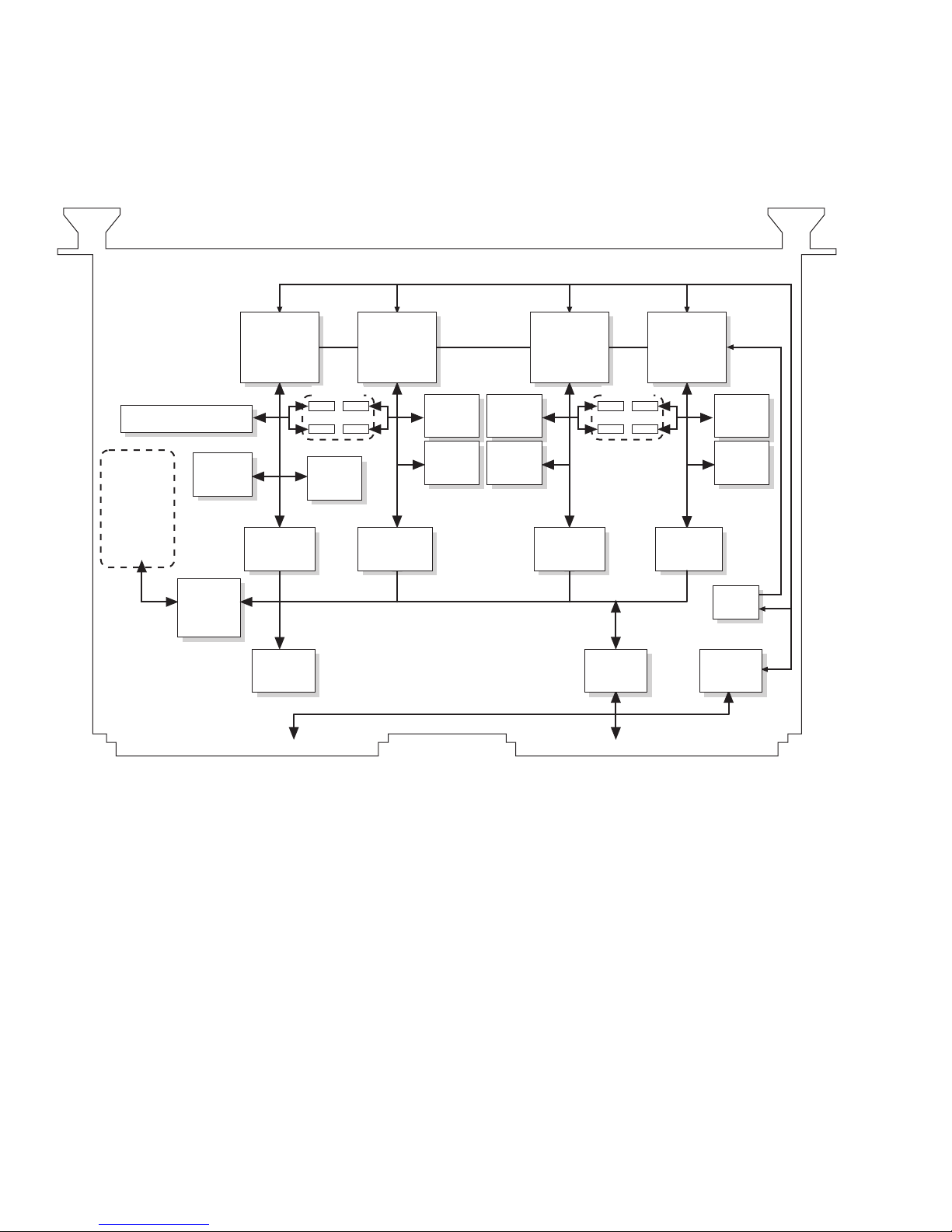
The following block diagram shows the main components of the Monaco board.
'C6x Host Port Inteface (HPI)
DSP~LINK3 Interface
SBSRAM
128K x 32
PMC
Site
PCI
Bus
Hurricane
Node A
'C6x
PEM Site
Address Buffer
and
Data Latches
Global Shared
SRAM
512K x 32
VME P2 Connector
SDRAM
4M x 32
Node B
'C6x
Address Buffer
and
Data Latches
SBSRAM
128K x 32
SDRAM
4M x 32
SBSRAM
128K x 32
SDRAM
4M x 32
Global Shared Bus
Node C
'C6x
Address Buffer
and
Data Latches
Node D
PEM Site
Address Buffer
Data Latches
SCV64
VME64
Interface
VME P1 Connector
'C6x
and
JT A G
SBSRAM
128K x 32
SDRAM
4M x 32
Test Bus
Controller
A24 VME
Slave
Interface
Figure 1 Block Diagram
1.5. On-Board Power Supply
There is an on-board high-efficiency DC-DC power converter that supplies +2.5V and
+3.3V power to the board from the VME 5V supply. The circuit efficiency is
approximately 90%. The +3.3V supply is available to the PEM and PMC sites, as well as
+5V and ±12V. Up to 16.5 Watts is available from the +3.3V supply for the PEM and
PMC sites. The combined +3.3V current consumption of modules on these sites must not
exceed 5 Amps.
When adding modules to the Monaco board, ensure that the power requirements for the
modules are within the specified limits, and that the system power supply and cooling are
sufficient to meet the added requirements.
4
Part Number 500-00191
Revision 2.00
Page 17
Spectrum Signal Processing Monaco Technical Reference
Introduction
1.6. Reset Conditions
The Monaco board responds to three types of reset conditions:
• VME SYSRESET (VME bus /SYSRESET line)
• VME A24 Slave Interface Reset (VME A24 Control Register bit D0)
• JTAG reset (JTAG chain /TRST line)
The following table indicates which hardware components are reset by the specific reset
condition.
Table 1 Reset Summary
Reset Condition (Y = Component is Reset)
Hardware SYSRESET Slave Interface Reset JTAG Reset
Processor Nodes Y Y
SCV64 VME Interface chip Y
HPI registers Y Y
Global Shared Bus registers Y Y
VME A24 slave interface registers Y Y
JTAG (within DSPs) Y Y Y
PEM interface Y Y
PMC interface Y Y
DSP~LINK3 interface Y Y
Part Number 500-00191
Revision 2.00
1.6.1. VME SYSRESET
A VME SYSRESET is initiated when the /SYSRESET line on the VME bus is driven
low. All devices and registers on the Monaco board are reset to their default conditions.
1.6.2. VME A24 Slave Interface Reset
The VME A24 slave interface reset is initiated from the VME bus by setting bit D0 of
the VME A24 Control Register to “0”. All devices and registers on the Monaco board
are reset to their default conditions except for the SCV64 VME interface chip. The
VME A24 Control Register is located at VME A24 Base Address + 1004h. The base
address for the VME A24 slave interface is set by jumper block JP1.
1.6.3. JTAG Reset
The JTAG path can be reset by asserting the /TRST line of the JTAG chain by an
EMURST from the XDS or TBC. Only the JTAG path of the DSPs is reset by this
action; no other devices or registers on the board are affected.
5
Page 18
Monaco Technical Reference Spectrum Signal Processing
Introduction
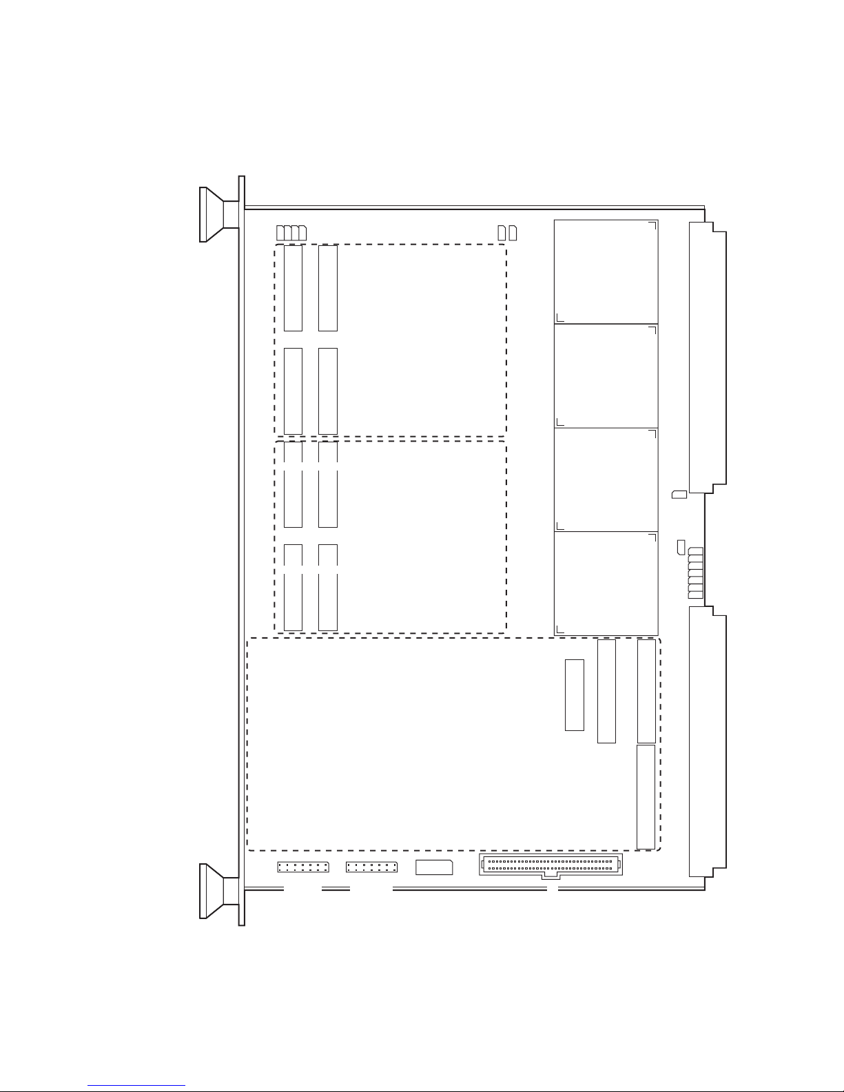
1.7. Board Layout
The following diagram shows the board layout of the Monaco board.
JP10 JP8JP9 JP7
JN6
JN8 JN9
JN10 JN11
JN12
JN7
JN13
PEM Site
Nodes C and D
PEM Site
Nodes A and B
JP4 JP5
Node D
‘C6x
Node C
‘C6x
Node B
‘C6x
Node A
‘C6x
JP3
JP2
JP1
12
34
56
78
89
10 11
12 13
VME
P1
JN1 JN2
JN5
VME
P2
J1
JTAG IN
Connector
J2
JTAG OUT
Connector
PMC Site
J3
DSP~LINK3 Ribbon Cable Connector
J8
JN4
Figure 2 Board Layout
6
Part Number 500-00191
Revision 2.00
Page 19
Spectrum Signal Processing Monaco Technical Reference
Introduction
1.8. Jumper settings
Table 2 Jumper Settings
Jumper Description IN OUT
JP1 Pins 1-2 VME A24 slave interface base address bit A23 0 1*
JP1 Pins 3-4 VME A24 slave interface base address bit A22 0* 1
JP1 Pins 5-6 VME A24 slave interface base address bit A21 0* 1
JP1 Pins 7-8 VME A24 slave interface base address bit A20 0* 1
JP1 Pins 9-10 VME A24 slave interface base address bit A19 0* 1
JP1 Pins 11-12 VME A24 slave interface base address bit A18 0* 1
JP1 Pins 13-14 VME A24 slave interface base address bit A17 0* 1
JP2 Node A boot mode PEM HPI*
JP3 Node B boot mode PEM HPI*
JP4 Node C boot mode PEM HPI*
JP5 Node D boot mode PEM HPI*
JP7 Node A Serial Port 1 Routing VME P2 PEM*
JP8 Node B Serial Port 1 Routing VME P2 PEM*
JP9 Node C Serial Port 1 Routing VME P2 PEM*
JP10 Node D Serial Port 1 Routing VME P2 PEM*
* Default position
Note:
The default VME A24 slave interface base address is set to 80 0000h.
Part Number 500-00191
Revision 2.00
7
Page 20

Monaco Technical Reference Spectrum Signal Processing
Introduction
8
Part Number 500-00191
Revision 2.00
Page 21
Spectrum Signal Processing Monaco Technical Reference
Processor Nodes
2 Processor Nodes
The Monaco board supports one, two or four embedded ‘C6X processor nodes shared
across the Global Shared Bus. The three possible processor configurations are described
in the following figure.
Table 3 Processor Configurations
Populated
Configuration Node A Node B Node C Node D
One Node Y
Two Nodes Y Y
Four Nodes YYYY
Each DSP node consists of:
• One TMS320C6201 DSP operating at 200 MHz for Monaco, or one TMS320C6701
DSP operating at 167 MHz for Monaco67
• 128K of 32-bit Synchronous burst SRAM (SBSRAM)
• 4M of 32-bit Synchronous DRAM (SDRAM)
• Processor Expansion Module (PEM) interface
• A slave Host Port Interface to VME A24 bus
• Two serial ports
• A DSP~LINK3 interface (DSP node A only)
Part Number 500-00191
Revision 2.00
9
Page 22
Monaco Technical Reference Spectrum Signal Processing
Processor Nodes
JT A G Test Bus
‘C6x Host Port
Interface (HPI) Bus
Node Local
Resources
Serial
Port 0
Serial
Port 1
DSP-LINK3
Interface
Node A
Only
PEM Site
Shared with
Node Pair
DSP
DSP
Local
Bus
‘C6x
128K x 32
SBSRAM
4M x 32
SDRAM
Address Buffer
and
Data Latches
Global Shared Bus
Figure 3 Processor Node Block Diagram
10
Part Number 500-00191
Revision 2.00
Page 23

Spectrum Signal Processing Monaco Technical Reference
Processor Nodes
2.1. Processor Memory Configurati on
Each ‘C6X DSP processor implements a 4 Gigabyte (full 32-bit) address space. This
address space is partitioned into internal memory space and external memory space.
External memory space is accessed through four memory select lines (CE0, CE1, CE2
and CE3).
2.1.1. Internal Memory
Internal memory space is further separated into three distinct regions:
• internal program RAM (64Kbytes)
• internal peripheral registers (2 Mbytes)
• internal data RAM (64 Kbytes)
These three regions define memory space which is implemented in the DSP processor.
2.1.2. External Memory
External memory is segmented into 4 regions:
• external memory interface CE0 (16 Mbytes)
• external memory interface CE1 (4 Mbytes)
• external memory interface CE2 (16 Mbytes)
• external memory interface CE3 (16 Mbytes)
External memory (CE0, CE1, CE2 and CE3) consists of node local memory resources
which are accessed on the DSP Local Bus, but are external to the DSP processor. The
type of memory in each of the four CE regions is determined by settings in the internal
peripheral registers. All remaining memory in the 4 GB address space is reserved.
The internal peripheral registers for Monaco must be initialized to the values in the
following table upon reset for the board to operate.
Part Number 500-00191
Revision 2.00
11
Page 24

Monaco Technical Reference Spectrum Signal Processing
Processor Nodes
Table 4 'C6x Internal Peripheral Register Values
Register
Global Control Register
Address
0x0180 0000
EMIF CE0 Control Register
0x0180 0008
EMIF CE1 Control Register
0x0180 0004
EMIF CE2 Control Register
0x0180 0010
EMIF CE3 Control Register
(Used for PEM. Must be
reconfigured for individual
PEM)
0x0180 0014
EMIF SDRAM Control
0x0180 0018
EMIF SDRAM Timing
0x0180 001C
Value Comments
0x0000 3078 NOHOLD (External HOLD disable) off
SDCEN (SDRAM clock enable) on
SSCEN (SBSRAM clock enable) on
CLK1EN (CLKOUT1 enable) on
CLK2EN (CLKOUT2 enable) on
SSCRT (SBSRAM clock rate select) 1/2x CPU clock
RBTR8 off (requester controls EMIF until a high priority request
occurs..
0xFFFF 3F43 MTYPE = 32 bit wide SBSRAM
No other bits are used.
0x30E4 0421 MTYPE = 32 bit wide asynchronous interface
write setup = 3 cycles
write strobe = 3 cycles
write hold = 2 cycles
read setup = 4 cycles
read strobe = 4 cycles
read hold = 1 cycle
all cycles are clockout1 cycles
0xFFFF 3F33 MTYPE = 32 bit wide SDRAM
No other bits are used.
0x72B7 0A23 MTYPE = 32 bit wide asynchronous interface
address = 0x01800004
value = 0x30E40421
MTYPE = 32 bit wide asynchronous interface
write setup = 7 cycles
write strobe = 10 cycles
write hold = 3 cycles
read setup = 7 cycles
read strobe = 10 cycles
read hold = 3 cycle
all cycles are clockout1 cycles
0x0544 A000 RFEN = 0 internal refresh enable OFF. Only external SDRAM
refresh can be used.
SDWID = 1 (SDRAM width select) two 16 bit SDRAMs
Other timing parameters are SDRAM specific and should not be
modified by the user.
0x0000 061A Refresh timer implemented in external hardware. This register is
not used.
12
Part Number 500-00191
Revision 2.00
Page 25
Spectrum Signal Processing Monaco Technical Reference
Processor Nodes
‘C6x Addr Memory Contents Memory Size
0000 0000 Internal-Program RAM 64 KB
0000 1000
Reserved 4 MB - 64KB
0040 0000 Local SBSRAM 512 KB
0048 0000
0140 0000
0180 0000
01A0 0000
0200 0000
0300 0000
External-Memory Space
Upon Reset
PEM EEPROM
Boot Mode
Internal-Peripheral Space 2 MB
Local SDRAM
Processor Expansion Module (PEM)
Reserved
CE1
CE0
External-Memory Space
After TOUT0 is toggled
DSP~LINK3
Shared SRAM
SCV64 Registers
(see the following CE1
memory map)
Reserved 6 MB
CE2
CE3
CE1
16 M - 512 KB
4 MB
16 MB
16 MB
Part Number 500-00191
Revision 2.00
0400 0000
Reserved 2 GB - 64 MB
8000 0000 Internal-Data RAM 64 KB
8001 0000
Reserved 2GB -
(2GB - 64 KB)
FFFF FFFF
Figure 4 DSP Memory Map
13
Page 26
Monaco Technical Reference Spectrum Signal Processing
Processor Nodes
External Memory Space CE1 is dedicated to accessing registers, global shared RAM and
DSP~LINK3 (Node A only). Node A differs from nodes B, C and D since it is the only
node with access to the DSP~LINK3. The following figure shows the memory map for
this region.
Address Node A Nodes B, C, and D
0140 0000
Global Shared SRAM
512K x 32
015F FFFC
0160 0000
DSP~LINK3 Standard Access
0163 FFFC
0164 0000
DSP~LINK3 Standard Fast Access Reserved
0167 FFFC
0168 0000
DSP~LINK3 RDY Controlled Access
016B FFFC
016C 0000
Hurricane Registers Hurricane Registers
016C 1FFC
016D 0000
Global Shared SRAM
512K x 32
016D 7FFC
016D 8000
016D FFFC
016E 0000
016E 7FFC
016E 8000
016E FFFC
016F 0000
016F FFFC
0170 0000
017F FFFC
Node A VPAGE Register Node B, C, or D VPAGE Register
Shared Bus Registers Shared Bus Registers
SCV64 Register Set (R/W) SCV64 Register Set (R/W)
Reserved Reserved
IACK Cycle Space (Read Only) IACK Cycle Space (Read Only)
One Mbyte window to the
VME Address Space
VME base address set by VPAGE register
DSP as VME Master (R/W)
VME base address set by VPAGE register
One Mbyte window to the
VME Address Space
DSP as VME Master (R/W)
Figure 5 DSP Memory Map for External-Memory Space CE1
14
Part Number 500-00191
Revision 2.00
Page 27

Spectrum Signal Processing Monaco Technical Reference
Processor Nodes
2.2. Synchronous Burst SRAM
The board provides 128K of 32-bit synchronous burst SRAM (SBSRAM) on each ‘C6x
local bus. The Monaco board supports 1 wait state operation.
2.3. Synchronous DRAM
The board provides 4M of 32-bit synchronous DRAM on each ‘C6x bus. The Monaco
board supports 1 wait state operation. An additional 4M of 32-bit synchronous DRAM
per DSP can also be supported on a PEM module.
Burst data transfer rates from CPU to SDRAM are 400 Mbytes/s on a Monaco with
200 MHz TMS320C6201 chips.
2.4. Processor Expansion Module
The Processor Expansion Module (PEM) provides a simple and flexible interface from
the DSP to I/O. It is similar to a PMC module, although physically narrower.
The Monaco board is designed to support two DSPs per PEM site, with a pair of
connectors for each DSP. While both DSP devices share the same PEM, the two DSP
buses are kept separate to allow very fast PEM data transfer rates.
The PEM is capable of booting the DSPs from local ROM, with up to 4 MBytes of
addressable boot space available to each DSP.
Refer to the PEM Specification for mechanical and functional details of the PEM
interface.
2.5. Host Port
A separate A24 VMEbus Slave interface is used for direct access to the DSP’s Host Port
Interface. This interface can be used for downloading code and as a control path from the
host to the DSP. Data transfer rates depend upon both the code executing in the DSP and
the VMEbus Master performing the transfers, but can be as high as 30 Mbytes/second.
Jumper block JP1 selects the VME A24 base address for this slave interface.
2.6. Interrupt Lines
There are four external interrupt inputs on each ‘C6x. They are INT4, INT5, INT6, and
INT7. All four must be configured as rising-edge triggered interrupts upon initialization.
See the Interrupt Handling chapter for further information.
Part Number 500-00191
Revision 2.00
15
Page 28

Monaco Technical Reference Spectrum Signal Processing
Processor Nodes
2.7. Processor Booting
The ‘C6x can boot from either the VME bus (via its Host Port Interface (HPI) port) or
from an 8-bit EEPROM on an installed PEM module. The jumpers listed in the following
table select the booting method for each node.
Table 5 Processor Boot Source Jumpers
Jumper Node PEM Boot HPI Boot
JP2 Node A IN OUT
JP3 Node B IN OUT
JP4 Node C IN OUT
JP5 Node D IN OUT
The Monaco board uses the CE1 memory space of the ‘C6x memory map 1 for the boot
space upon power up or reset. Immediately after booting, the ‘C6x cannot access the
resources in its CE1 space such as the Hurricane registers, Global Shared SRAM, and
SCV64 Registers. In order to access these CE1 resources, the ‘C6x must toggle the state
of its Timer 0 pin (TOUT0). The state of this pin is controlled by the DataOut bit of the
‘C6x Timer 0 Control Register. Once TOUT has been toggled, the CE1 resources are
available to the ‘C6x until the ‘C6x is reset.
16
Part Number 500-00191
Revision 2.00
Page 29

Spectrum Signal Processing Monaco Technical Reference
Processor Nodes
2.8. Serial Port Routing
Each ‘C6x has two serial ports. Serial Port 0 of each DSP is routed to the PEM connector
associated with the DSP node.
Routing for Serial Port 1 on nodes A, B, C and D is determined by jumpers J7 to J10 as
shown in the figure and following tables. The jumper setting selects routing either to the
PMC JN5 and VME P2 connectors, or to the PEM connector associated with the DSP
node.
Serial Port routing for the Monaco board is shown the figure. Complete pinouts for the
connectors are given in the Connector Pinouts chapter.
Serial
Port 0
Serial
Port 1
Serial
Port 0
Serial
Port 1
Serial
Port 0
Serial
Port 1
Serial
Port 0
Serial
Port 1
Node D
C6x
Node C
C6x
Node B
C6x
Node A
C6x
VME
P1
Node
D
PEM
1
Node
C
PEM
1
Node
B
PEM
1
Node
A
PEM
1
Node
D
PEM
2
Node
C
PEM
2
Node
B
PEM
2
Node
A
PEM
2
OUT
OUT
JP7
IN
OUT
JP8
IN
OUT
JP9
IN
JP10
IN
Figure 6 Serial Port Routing
Part Number 500-00191
Revision 2.00
Node D Serial Port 0
Node C Serial Port 0
Node B Serial Port 0
Node A Serial Port 0
PMC
Connector
JN5
Node D
Node C
Node B
Node A
VME
P2
17
Page 30

Monaco Technical Reference Spectrum Signal Processing
Processor Nodes
Pin assignments for the serial ports are given in the following tables.
Table 6 PEM Connections for Serial Port 0 and 1
Signal PEM 1 Port 0 PEM 2 Port 1*
CLKS External clock 56 17
CLKR Receive clock 52 13
CLKX Transmit clock 42 3
DR Received serial data 48 9
DX Transmitted serial data 46 7
FSR Receive frame synchronization 50 11
FSX Transmit frame synchronization 44 5
*The serial port routing jumper corresponding to the node (J7, J8, J9, or J10) must be
OUT for port 1 to be routed to the node’s PEM 2 connector.
Table 7 VME and PMC Connections for Serial Port 1
Node A (J7 IN) Node B (J8 IN) Node C (J9 IN) Node D (J10 IN)
Signal PMC JN5 VME-P2 PMC JN5 VME-P2 PMC JN5 VME-P2 PMC JN5 VME-P2
CLKS External clock 1 D-4 21 D-18 2 Z-3 22 Z-17
CLKR Receive clock 5 D-6 25 D-20 6 Z-5 26 Z-19
CLKX Transmit clock 9 D-8 29 D-22 10 Z-7 30 Z-21
DR Received serial data 11 D-10 31 D-24 12 Z-9 32 Z-23
DX Transmitted serial data 13 D-12 33 D-26 14 Z-11 34 Z-25
FSR Receive frame synchronization 15 D-14 35 D-28 16 Z-13 36 Z-27
FSX Transmit frame synchronization 17 D-16 37 D-30 18 Z-15 38 Z-29
18
Part Number 500-00191
Revision 2.00
Page 31

Spectrum Signal Processing Monaco Technical Reference
Global Shared Bus
3 Global Shared Bus
The Global Shared Bus provides access between devices on the Monaco board as shown
in the following table.
Table 8 Global Shared Bus Access
Source
3.1. Memory
Target ‘C6x
Nodes
Internal program & data RAM R/W own node No Access No Access
Local SDRAM R/W own node No Access No Access
Local SBSRAM R/W own node No Access No Access
Global Shared RAM R/W (32-bit only) R/W R/W
Hurricane Registers R/W R/W R/W
PMC Site Hurricane DMA
access only
SCV64 Registers R/W No Access No Access
Global Shared Bus Registers R/W No Access No Access
VMEbus as master R/W No Access -
PMC
Site
- No Access
VME Bus
via SCV64
512K of 32-bit Asynchronous RAM, implemented in four 512K x 8-bit Asynchronous
RAM devices, is provided on the Global Shared Bus. The ‘C6x DSPs can only perform
32-bit accesses to the Global Shared RAM. Byte accesses are not supported.
3.2. Arbitration
Arbitration of the Global Shared Bus is implemented using a next bus owner token that is
passed serially from one device to the next. Token passing follows a strict hierarchical
sequence, ordered by bus servicing priority. There are six devices participating in the
process. These are, in decreasing priority:
• SCV64
• Hurricane
• DSP Node A
• DSP Node B
• DSP Node C
• DSP Node D
Part Number 500-00191
Revision 2.00
19
Page 32

Monaco Technical Reference Spectrum Signal Processing
Global Shared Bus
Bus ownership is cycled between the two highest priority devices (SCV64 and
Hurricane) until neither device requires the bus. Then the DSP Nodes are processed
round robin. After one pass through the DSP chain, the cycle loops back to include the
SCV64 and Hurricane. This eliminates any arbitration latency as bus ownership is
transferred between devices, and grants the highest priority to those devices interfacing
to external buses (VME and PCI), which require the fastest response. The arbitration
cycle is shown in the following figure.
Note:
Because there is no ownership timer for either Hurricane or SCV64 chip
the system designer must ensure that processors are not held off from the shared
resources for unreasonable lengths of time.
Highest Priority Lowest priority
Node AHurricaneSCV64 Node DNode CNode B
Round Robin
DSPVME & PCI Bus
Round Robin
Figure 7 Global Bus Arbitration
Access to the Global Shared Bus can use single, burst, or locked cycles.
20
3.2.1. Single Cycle Bus Access
For single cycle accesses a device requests the global shared bus by simply initiating a
read or write access to the bus. When the bus is free, the device acquires it and performs
the single cycle access. The bus is then released.
3.2.2. Burst Cycle Bus Access
Burst cycles are used during DMA transfers from a ‘C6x processor to the Global Shared
Bus. A 6-bit bus ownership timer on each node prevents a ‘C6x from owning the bus for
more than 640 ns when another device is requesting the bus. When the burst cycles are
begun, the timer is started. If another device requests the bus when the timer expires, the
bus is released; otherwise ownership is maintained and the timer is reset and started
again.
If multiple DSPs request the bus, this scheme allocates time to them fairly so that none
are locked out.
Part Number 500-00191
Revision 2.00
Page 33

Spectrum Signal Processing Monaco Technical Reference
Global Shared Bus
Although this is a non-prioritized scheme, the back-off function of the SCV64 interface
resolves collisions between a bus master and the VMEbus if there is contention for the
VMEbus.
Note:
There are no ownership timers for the Hurricane or SCV64. If the
Hurricane holds the bus too long the VME bus could timeout.
3.2.3. Locked Cycles
A ‘C6x can lock the Global Shared Bus in order to perform Read-Modify-Write (RMW)
or other atomic accesses to it, by driving its Timer 0 (TOUT0) low. After the TOUT0 is
driven low, the next access to the Global Shared Bus acquires the bus. The bus is not
released until the ‘C6x drives the Timer 0 (TOUT0) pin high.
Caution:
be used carefully because other devices will not acquire the bus once it is locked.
This capability is intended for read-modify-write accesses to the Global Shared
RAM and registers. It is highly recommended that Bus locking not be used. It
can lead to a deadlock condition, and in particular, result in debugger timeouts.
The following precautions should be observed when locking the Global Shared Bus:
1. VME bus timeouts can occur because the SCV64 cannot access the board while a
‘C6x has locked the bus.
The capability of locking the Global Shared Bus from a ‘C6x should
2. If node A accesses the DSP~LINK3 interface while it has locked the Global Shared
Bus by asserting TOUT0, the bus will be released. Node A’s next access to the bus
will re-lock it to node A, providing that TOUT0 is still asserted.
3. Some SCV64 inbound cycles can occur while the bus is locked. If a ‘C6x has locked
the bus and is performing a VME outbound cycle while a VME inbound cycle is in
progress, the ‘C6x will be temporarily backed off and the SCV64 cycle will proceed.
The Global Shared Bus will be returned to that ‘C6x node after the SCV64 cycle
finishes. No other ‘C6x will get ownership of the bus.
4. If a debugger is being used when one processor has the bus locked for an extended
time while another processor is trying to get the bus, the debugger may timeout.
Part Number 500-00191
Revision 2.00
21
Page 34

Monaco Technical Reference Spectrum Signal Processing
Global Shared Bus
22
Part Number 500-00191
Revision 2.00
Page 35

Spectrum Signal Processing Monaco Technical Reference
VME64 Bus Interface
4 VME64 Bus Interface
There are two separate VMEbus slave interfaces on the Monaco board. One is
implemented by the SCV64 and provides A32 and A24 VMEbus masters access to the
global shared bus. The second slave interface provides direct access to the Test Bus
Controller for debugging, and to the Host Port Interfaces (HPIs) of each ‘C6x. The HPI
provides support for code download, control, and data transfers from the VME64 bus.
4.1. VME Operation
The Monaco board requires a VME chassis (6U) with power supply. The board
automatically becomes VMEbus system controller (Syscon) if it resides at the top of the
VMEbus grant daisy chain. This capability is provided by the Tundra SCV64 interface
chip. Refer to the SCV64 User Manual for details.
The Monaco board has two VME backplane connectors: a 3 row P1 connector and a 5
row P2 connector.
The board may be installed in either a 5 row VME backplane or a 3 row backplane. The
two additional rows on the VME P2 connector (Z and D) only serve to route serial port
signals from DSP processor nodes A, B, C and D to the VME backplane, if the board is
configured for that option.
Note:
routing will be restricted to the PEM and PMC sites only.
If the Monaco board is installed in a 3 row VME chassis, serial port
4.2. SCV64 Primary Slave A32/A24 Interface
The primary interface to the VME64 bus is based on Tundra Semiconductor
Corporation’s SCV64 VME64 Interface chip. This chip enables the Monaco board to act
as a master or a slave on the VME64 bus, and also provides VME interrupt capabilities.
Transfer rates of 40 MBytes/sec are supported between the SCV64 and the Global
Shared Bus SRAM once the bus has been acquired. The SCV64 cannot be pre-empted
from the Global Shared Bus and it does not have a bus ownership timer.
A host on the VME64 bus can access both the lower half (1 Mbyte) of Global SRAM
and the Hurricane control registers on a Monaco board in either A24 or A32 addressing
modes as shown in the following memory map.
Part Number 500-00191
Revision 2.00
23
Page 36

Monaco Technical Reference Spectrum Signal Processing
VME64 Bus Interface
VME Offset Address Access
0000 0000h
Global Shared SRAM
(lower 1Mbyte)
000F FFFFh
0010 0000h
Global Shared SRAM
(Upper 1 Mbyte)
001F FFFFh
0020 0000h
Hurricane Control Registers
002F FFFFh
0030 0000h
Reserved
003F FFFFh
Host
VME DSP
accessible and
Figure 8 Primary VME A24/A32 Memory Map
Note:
The full A24 memory map occupies one-quarter of the available A24
space. This can be reduced to the standard 512K (16M ÷ 32) of the available
A24 space by mapping only the lower 512 Kbytes (128k x 32) of the global
shared SRAM. This is entirely programmable in the SCV64 base address
registers. Only SCV64 A21 and A20 are used for decode on SCV64 VME slave
accesses to the board. D16 and D08E0 writes are not supported on the primary
A32/A24 interface.
Hurricane
accessible
4.3. A24 Secondary Slave Interface
Jumper block JP1 sets address bits A23..A17 of the VME A24 slave interface. This base
address defines a 128K byte addressed memory space accessed by the VME bus. Access
to this space from the VME bus bypasses the SCV64 VME bus interface chip.
All A24 VME transfer types are accepted except for LOCK, and MBLT types.
As shown in the following memory map, the A24 slave interface provides the VME bus
direct access to:
• The Host Port Interface (HPI) registers of each ‘C6x processor
• The Test Bus Controller (TBC) for JTAG debugging operation
• Control and Status registers of the Monaco board
D16 and D08E0 accesses are not supported on the slave A24 secondary interface.
24
Part Number 500-00191
Revision 2.00
Page 37

Spectrum Signal Processing Monaco Technical Reference
VME64 Bus Interface
VME Offset Address
00 0000h
Test Bus Controller Registers (JTAG)
00 0FFFh
00 1000h
FPGA
‘C6x
‘C6x
00 1003h
00 1004h
00 1007h
00 1008h
00 1FFFh
00 2000h
00 2FFFh
00 3000h
00 3FFFh
00 4000h
00 4FFFh
00 5000h
00 5FFFh
00 6000h
00 FFFFh
01 0000h
01 3FFCh
01 4000h
01 3FFCh
01 B000h
01 3FFCh
01 C000h
01 FFFCh
VME A24 Status Register (Read Only)
VME A24 Control Register (Read/Write)
Reserved
Node A HPI Registers
Node B HPI Registers
Node C HPI Registers
Node D HPI Registers
Reserved
Node A HPID DMA Space (HPIA incremented)
all addresses mapped to 00 2008h
Node B HPID DMA Space (HPIA incremented)
all addresses mapped to 00 3008h
Node C HPID DMA Space (HPIA incremented)
all addresses mapped to 00 4008h
Node D HPID DMA Space (HPIA incremented)
all addresses mapped to 00 5008h
16 KB
16 KB
16 KB
16 KB
Figure 9 A24 Secondary Interface Memory Map
Refer to the JTAG Debugging chapter for information on using the Test Bus Controller
for JTAG operation. The VME A24 Status Register and the
VME A24 Control Register are described in the Registers chapter.
Part Number 500-00191
Revision 2.00
25
Page 38

Monaco Technical Reference Spectrum Signal Processing
VME64 Bus Interface
The Host Port Interface (HPI) allows a VME host to access the memory map of any
‘C6X. The board transfers 32-bit VME accesses automatically through the 16-bit Host
Port Interface as two 16-bit words. The interface consists of three read/write, 32-bit
registers that are accessed through the VME A24 slave interface:
• HPI Address register (HPIA)
• HPI Control register (HPIC). A ‘C6x can also read and write to its HPI Control
register (HPIC) at address 0188 0000h.
• HPI Data register (HPID)
VME address bits A[3:2] select which register is being accessed in each node’s HPI
register address space. These bits are mapped to the HCNTRL[1:0] control pins of the
‘C6x. The following table shows how the HPI interface is addressed.
Table 9 HPI Register Addresses
VME address
‘C6x
Register
HPIC 00 2000h 00 3000h 00 4000h 00 5000h State for reading/setting the Control Register value.
HPIA 00 2004h 00 3004h 00 4004h 00 5004h Used to read/set the HPI address pointer. The HPIA
HPID 00 2008h 00 3008h 00 4008h 00 5008h A VME host reads and writes data to this address for
HPID 00 200Ch 00 300Ch 00 400Ch 00 500Ch A VME host reads and writes data to this address for
HPID
DMA
Space
Node
A
01 0000h 01 4000h 01 8000h 01 C0000h VME hosts which increment their target address can use
Node
B
Node
C
Node
D Description
points into the C6x memory space.
DMA transfers to the HPID register. The HPIA register
automatically increments by 4 bytes as each word is
transferred through the HPID register.
single cycle transfers to the HPID register. The HPIA is
not incremented for this HPI access mode.
this address space for DMA transfers to the HPID
register. Up to 4K of 32-bit data can be transferred in this
space. Data written to this space is automatically
transferred to the HPID register, and the HPIA register
automatically increments by 4 bytes as each word is
transferred.
26
Part Number 500-00191
Revision 2.00
Page 39

Spectrum Signal Processing Monaco Technical Reference
VME64 Bus Interface
Before a host can transfer data through a node’s HPI, the VME host must set the HWOB
bit of the node’s HPIC register to “1”. This only has to be done once after the Monaco
board is reset. To access an address within a ‘C6x’s memory space, the VME host loads
the address into the HPIA register. Data is then transferred through the HPID register.
• The HPID at offset “8h” auto-increments four bytes after every cycle, allowing it to
be used for burst DMA data transfers.
• The HPID at offset “Ch” does not auto-increment, and is therefore intended for
single cycle accesses only.
• The HPID DMA Space offers a 16K address space to VME hosts which increment
their target address during DMA transfers. This allows them to transfer data in
blocks of 16K 32-bit words to the HPID register used for DMA transfers.
4.4. Master A32/A24/A16 SCV64 Interface
As a VME master, the Monaco board supports A16, A24, or A32 transactions from any
node to the VME64 bus through the SCV64 chip. Any node can program the SCV64’s
DMA Controller for VME Master Accesses, and can directly master the VMEbus. Each
node has its own VPAGE Register to support the KFC, KSIZE, and upper 12 and
lower 2 address bits to the SCV64. The upper 11 bits extend the 20-bit address space of
the ‘C6x to the full 32-bit address space of the VME bus. Any node can monitor the
status of the /KIPL interrupt lines, BUSERRORs for each node, and KAVEC line by
reading the VSTATUS Register.
The Monaco board supports Auto-Syscon capabilities allowing it to become the System
Controller board when placed in the leftmost slot of the VME backplane. If it is to be the
System Controller it should typically be booted from a PEM module equipped with a
boot PROM.
Upon reset, the SCV64 is in Bus-Isolation Mode (BI-Mode) which isolates the SCV64
from the VME64 bus. The SCV64 is released from BI-Mode by a write to the SCV64
Location Monitor from any node of the Monaco board.
Part Number 500-00191
Revision 2.00
27
Page 40

Monaco Technical Reference Spectrum Signal Processing
VME64 Bus Interface
28
Part Number 500-00191
Revision 2.00
Page 41

Spectrum Signal Processing Monaco Technical Reference
DSP~LINK3 Interface
5 DSP~LINK3 Interface
The Monaco board provides a DSP~LINK3 interface through a ribbon cable connector.
The interface supports up to 4 slave DSP~LINK3 devices. The ribbon cable can be up to
12 inches (30 cm) long.
The DSP~LINK3 interface is accessed from node A’s local bus only; it is not accessible
from any other node nor from the VME bus. Accesses to the DSP~LINK3 interface do
not require the Global Shared Bus. As a result, DSP~LINK3 accesses can happen
concurrently with Global Shared Bus access by other devices (such as the other
processors or the SCV64 chip).
If a DSP~LINK3 access is interleaved within global shared SRAM accesses, node A
acquires the Global Shared Bus, performs the SRAM access, releases the Global Shared
Bus, performs the DSP~LINK3 access, acquires the Global Shared Bus, and then
performs the next Global Shared Bus SRAM access using a control register.
5.1. DSP~LINK3 Data Transfer Operating Modes
The Monaco board supports four data transfer operating modes.
• Standard Access
• Standard Fast Access
• Address Strobe Control
• Ready Control Access
The three “access” data transfer operating modes (Standard, Standard Fast and Ready
Control) of the DSP~LINK3 interface use three 64K address spaces accessed from node
A. Each of the three “access” modes is assigned its own 64K memory space. Address
Strobe Control cycles are multiplexed with the Standard Fast Access mode space.
The following table shows how the DSP~LINK3 data transfer operating modes are
supported.
Part Number 500-00191
Revision 2.00
29
Page 42

Monaco Technical Reference Spectrum Signal Processing
DSP~LINK3 Interface
Table 10 DSP~LINK3 Data Transfer Operating Modes
Mode
Standard
Access
Standard
Fast
Access
Address
Strobe
Control
Ready
Control
Access
Base
Address
0160 0000h
0164 0000h 0 For DSP~LINK3 slave boards that have fast,
0164 0000h 1 For slave boards that require more than the
0168 0000h
ASTRB_EN
Bit Description
x
x
For slave boards that are similar to DSP~LINK1
slave boards and operate with a fixed access
time.
fixed access time. This memory space is
shared with the Address Strobe Control
operating mode.
16 KWords of addressing provided by the
standard DSP~LINK3 address lines. The bus
master uses the /ASTRB cycle to place the
page address onto the DSP~LINK3 data lines.
It determines which address page is accessed
on the slave board. This allows access to up to
14
address pages with each address page
2
having an address depth of 2
Cycle has the same timing as the Standard
Fast transfer cycle.
For DSP~LINK3 slave boards that require
variable length access times. /DSTRB is active
until the slave asserts the DSP~LINK3 ready
signal (/RDY) to end the cycle.
14
. The /ASTRB
5.2. Address Strobe Control Mode
The Address Strobe Control mode uses the same node A 64K address space as the
Standard Fast Access mode. The Address Strobe Control mode is enabled for this space
by setting bit D1, the ASTRB_EN bit, of the DSP~LINK3 register to “1”. This register is
located at address 016D 8018h of node A. Standard Fast Access mode writes will now
generate /ASTRB cycles. The DSP~LINK3 slave attached to the Monaco board should
then latch the lower addresses.
30
Part Number 500-00191
Revision 2.00
Page 43

Spectrum Signal Processing Monaco Technical Reference
DSP~LINK3 Interface
5.3. Interface Signals
The DSP~LINK3 interface consists of two 16-bit bi-directional buffers for data, a 16-bit
address latch, and a control signal buffer. The control signals are terminated via a SCSI
terminator. The DSP~LINK3 interface signals are:
• 32 data I/O lines: D[31..0]
• 16 address outputs: A[15..0] A15 and A14 are used for slave device (board)
selection.
• /DSTRB, /ASTRB, R/W and /RST outputs
• Tri-state ready (/RDY) input
• 4 open-collector interrupt inputs (IRQ0 to IRQ3). These interrupt are logically
OR’ed and routed to the INT7 line of node A’s ‘C6x.
Refer to DSP~LINK3 specification for details (available from Spectrum’s internet web
site at http://www.spectrumsignal.com)
5.4. DSP~LINK3 Reset
Bit D0 of the DSP~LINK3 register controls the DSP~LINK3 reset line. This register is
located at address 016D 8018h of node A. Setting bit D0 to “1” asserts the DSP~LINK3
reset line; setting it to “0” releases the reset. DSP~LINK3 resets must be at least 1 µs
long. This reset is entirely under software control.
The DSP~LINK3 reset line will also be asserted during /SYSRESET or secondary
control register board reset conditions.
Part Number 500-00191
Revision 2.00
31
Page 44

Monaco Technical Reference Spectrum Signal Processing
DSP~LINK3 Interface
32
Part Number 500-00191
Revision 2.00
Page 45

Spectrum Signal Processing Monaco Technical Reference
PCI Interface
6 PCI Interface
The Hurricane chip provides the interface between the Global Shared SRAM on the
Global Shared Bus and the PMC site which supports a 32 bit, 33 MHz PCI bus. Although
the DSPs cannot directly master the PCI bus, the Hurricane’s DMA controller provides
flexible data transfer between the Global Shared Bus SRAM and the PMC.
Embedded PCI buses require Hurricane PCI configuration cycle generation.
Pre-emptive arbitration is not used. If a node requests the Global Shared bus when the
bus is not currently in use, then it will be granted the bus. It is up to the bus ownership
timers of the Hurricane and PMC devices to prevent bus hogging.
PMC modules can directly master the Global Shared SRAM.
The memory map of the Monaco seen by a PMC module is shown in the following
figure.
PCI Offset Address Access
0000 0000h
001F FFFFh
0020 0000h
002F FFFFh
0030 0000h
003F FFFFh
Figure 10 PCI Memory Map
6.1. Hurricane Configuration
Before the PMC site can be accessed, the Monaco initialization software must configure
the Hurricane registers with the values shown in the following table. Only the indicated
values should be initialized, all other values should be left alone. As can be seen, these
registers can be accessed from a ‘C6x, the PMC’s PCI bus, and a host on the VME bus.
Global Shared SRAM
Hurricane Control Registers
Reserved
Part Number 500-00191
Revision 2.00
33
Page 46

Monaco Technical Reference Spectrum Signal Processing
PCI Interface
Table 11 Hurricane Register Set
Hurricane
DSP Offset
0x00 0x016C 0000 0x0020 0000 0x0020 0000 DCSR DMA Control / Status Register 0x0000 0000
0x01 0x016C 0004 0x0020 0004 0x0020 0004 IFSC Interrupt Flag, Set, Clr 0x0000 0000 Y
0x02 0x016C 0008 0x0020 0008 0x0020 0008 IED Interrupt Enable to DSP 0x0000 0000 Y
0x03 0x016C 000C 0x0020 000C 0x0020 000C IEP Interrupt Enable to PCI 0x0000 0000
0x04 0x016C 0010 0x0020 0010 0x0020 0010 IT Interrupt type 0x0000 0006 Y
0x05 0x016C 0014 0x0020 0014 0x0020 0014 GCSR General control and status register 0x1F00 0011
0x06 0x016C 0018 0x0020 0018 0x0020 0018 TTP Timer trigger point 0x0000 0001
0x07 0x016C 001C 0x0020 001C 0x0020 001C TV Timer value 0x0000 0000
0x08 0x016C 0020 0x0020 0020 0x0020 0020 SCR Serial EEPROM control 0x0000 302C
0x09 0x016C 0024 0x0020 0024 0x0020 0024 SEA Serial EEPROM address 0x0000 0000
0x0A 0x016C 0028 0x0020 0028 0x0020 0028 SED Serial EEPROM data 0x0000 0000
0x0B 0x016C 002C 0x0020 002C 0x0020 002C PFR Pin Function Register 0x0000 0000
0x0C 0x016C 0030 0x0020 0030 0x0020 0030 reserved 0x0000 0000
0x0D 0x016C 0034 0x0020 0034 0x0020 0034 reserved 0x0000 0000
0x0E 0x016C 0038 0x0020 0038 0x0020 0038 REV Chip Rev Code 0x0000 0010
0x0F 0x016C 003C 0x0020 003C 0x0020 003C RAC Register access control 0x0000 0100
0x10 0x016C 0040 0x0020 0040 0x0020 0040 DDA DSP Address 0x0000 0000
0x11 0x016C 0044 0x0020 0044 0x0020 0044 DPA PCI Address 0x0000 0000
0x12 0x016C 0048 0x0020 0048 0x0020 0048 DLNGTH Length 0x0000 0000
0x13 0x016C 004C 0x0020 004C 0x0020 004C DINTP Interrupt Point 0x0000 0000 Y
0x14 0x016C 0050 0x0020 0050 0x0020 0050 DSTRD DSP Stride 0x0000 0000
0x15 0x016C 0054 0x0020 0054 0x0020 0054 DPC Packet Control 0x0000 00F6 Y
0x16 0x016C 0058 0x0020 0058 0x0020 0058 DCAR DMA Chain Address Register 0x0000 0000
0x17 0x016C 005C 0x0020 005C 0x0020 005C reserved 0x0000 0000
0x18 0x016C 0060 0x0020 0060 0x0020 0060 DCDA Current DSP Address 0x0000 0000
0x19 0x016C 0064 0x0020 0064 0x0020 0064 DCPA Current PCI Address 0x0000 0000
0x1A 0x016C 0068 0x0020 0068 0x0020 0068 DCLNTGH Current Length 0x0000 0000
0x1B 0x016C 006C 0x0020 006C 0x0020 006C DBC PCI DMA burst control 0x0020 0020
0x1C 0x016C 0070 0x0020 0070 0x0020 0070 DFC DMA FIFO Control 0x0000 0620
0x1D 0x016C 0074 0x0020 0074 0x0020 0074 DBE PCI byte enable and command register 0x0000 0000
0x1E 0x016C 0078 0x0020 0078 0x0020 0078 0x0000 0000
0x1F 0x016C 007C 0x0020 007C 0x0020 007C 0x0000 0000
0x20 0x016C 0080 0x0020 0080 0x0020 0080 BCC0A DSP Cycle control 0A 0x0010 0021 Y
0x21 0x016C 0084 0x0020 0084 0x0020 0084 BCC0B DSP Cycle control 0B 0x0000 0140 Y
0x22 0x016C 0088 0x0020 0088 0x0020 0088 BCC0C DSP Cycle control 0C 0xB401 6820 Y
0x23 0x016C 008C 0x0020 008C 0x0020 008C BCC0D DSP Cycle control 0D 0x2800 2800 Y
0x24 0x016C 0090 0x0020 0090 0x0020 0090 BCC1A DSP Cycle control 1A 0x0000 0000
0x25 0x016C 0094 0x0020 0094 0x0020 0094 BCC1B DSP Cycle control 1B 0x0000 0000
0x26 0x016C 0098 0x0020 0098 0x0020 0098 BCC1C DSP Cycle control 1C 0x0000 0000
0x27 0x016C 009C 0x0020 009C 0x0020 009C BCC1D DSP Cycle control 1D 0x0000 0000
'C6x
Address
PCI Bus
Offset
Slave A32/A24
SCV64 Offset
Register Description Value Initialize
34
Part Number 500-00191
Revision 2.00
Page 47

Spectrum Signal Processing Monaco Technical Reference
PCI Interface
Hurricane
DSP Offset
0x28 0x016C 00A0 0x0020 00A0 0x0020 00A0 BCC2A DSP Cycle control 2A 0x0000 0000
0x29 0x016C 00A4 0x0020 00A4 0x0020 00A4 BCC2B DSP Cycle control 2B 0x0000 0000
0x2A 0x016C 00A8 0x0020 00A8 0x0020 00A8 BCC2C DSP Cycle control 2C 0x0000 0000
0x2B 0x016C 00AC 0x0020 00AC 0x0020 00AC BCC2D DSP Cycle control 2D 0x0000 0000
0x2C 0x016C 00B0 0x0020 00B0 0x0020 00B0 BCC3A DSP Cycle control 3A 0x00D6 1DE0
0x2D 0x016C 00B4 0x0020 00B4 0x0020 00B4 BCC3B DSP Cycle control 3B 0x0000 0000
0x2E 0x016C 00B8 0x0020 00B8 0x0020 00B8 BCC3C DSP Cycle control 3C 0xA9E0 69A0
0x2F 0x016C 00BC 0x0020 00BC 0x0020 00BC BCC3D DSP Cycle control 3D 0x0000 0000
0x30 0x016C 00C0 0x0020 00C0 0x0020 00C0 BMI0 Bank 0 Mapping Information 0x1000 0003 Y
0x31 0x016C 00C4 0x0020 00C4 0x0020 00C4 BMI1 Bank 1 Mapping Information 0x0000 0000
0x32 0x016C 00C8 0x0020 00C8 0x0020 00C8 BMI2 Bank 2 Mapping Information 0x0000 0000
0x33 0x016C 00CC 0x0020 00CC 0x0020 00CC BMI3 Bank 3 Mapping Information 0x0000 0000
0x34 0x016C 00D0 0x0020 00D0 0x0020 00D0 BMI4 Bank 4 Mapping Information 0x0000 0000
0x35 0x016C 00D4 0x0020 00D4 0x0020 00D4 BMI5 Bank 5 Mapping Information 0x0000 0000
0x36 0x016C 00D8 0x0020 00D8 0x0020 00D8 BMI6 Bank 6 Mapping Information 0x0000 0000
0x37 0x016C 00DC 0x0020 00DC 0x0020 00DC BMI7 Bank 7 Mapping Information 0x0000 0000
0x38 0x016C 00E0 0x0020 00E0 0x0020 00E0 BMI8 Bank 8 Mapping Information 0x0000 0000
0x39 0x016C 00E4 0x0020 00E4 0x0020 00E4 CSCR Cycle select (all banks) 0x0000 0000 Y
0x3A 0x016C 00E8 0x0020 00E8 0x0020 00E8 MABE
0x3B 0x016C 00EC 0x0020 00EC 0x0020 00EC IRBAR Internal Register Base Address Register 0x0020 0000 Y
0x3C 0x016C 00F0 0x0020 00F0 0x0020 00F0 PCS Programmable Chip Select 0x0000 0000 Y
0x3D 0x016C 00F4 0x0020 00F4 0x0020 00F4 DSPBT DSP bus timer control register 0x0000 0000
0x3E 0x016C 00F8 0x0020 00F8 0x0020 00F8 DBIC DSP bus interface control 0x0000 0000
0x3F 0x016C 00FC 0x0020 00FC 0x0020 00FC reserved 0x0000 0000
0x40 0x016C 0100 0x0020 0100 0x0020 0100 0xFFFF12FB
0x41 0x016C 0104 0x0020 0104 0x0020 0104 0x0280 0006
0x42 0x016C 0108 0x0020 0108 0x0020 0108 0x0680 0000
0x43 0x016C 010C 0x0020 010C 0x0020 010C 0x0000 0000
0x44 0x016C 0110 0x0020 0110 0x0020 0110 0x0000 0000
0x45 0x016C 0114 0x0020 0114 0x0020 0114 0x0000 0000
0x46 0x016C 0118 0x0020 0118 0x0020 0118 PCI Configuration Registers 0x0000 0000
0x47 0x016C 011C 0x0020 011C 0x0020 011C 0x0000 0000
0x48 0x016C 0120 0x0020 0120 0x0020 0120 0x0000 0000
0x49 0x016C 0124 0x0020 0124 0x0020 0124 0x0000 0000
0x4A 0x016C 0128 0x0020 0128 0x0020 0128 0x0000 0000
0x4B 0x016C 012C 0x0020 012C 0x0020 012C 0xFFFF FFFF
0x4C 0x016C 0130 0x0020 0130 0x0020 0130 0x0000 0000
0x4D 0x016C 0134 0x0020 0134 0x0020 0134 0x0000 0000
0x4E 0x016C 0138 0x0020 0138 0x0020 0138 0x0000 0000
'C6x
Address
PCI Bus
Offset
Slave A32/A24
SCV64 Offset
Register Description Value Initialize
CSER
BER
Map Bank Enable
Chip Select Enable
Mask Broadcast
0x0001 0100 Y
Part Number 500-00191
Revision 2.00
35
Page 48

Monaco Technical Reference Spectrum Signal Processing
PCI Interface
Hurricane
DSP Offset
0x4F 0x016C 013C 0x0020 013C 0x0020 013C 0x0120 0100
0x50 0x016C 0140 0x0020 0140 0x0020 0140 BAR0 Shadow Register 0xFF00 0000 Y
'C6x
Address
PCI Bus
Offset
Slave A32/A24
SCV64 Offset
Register Description Value Initialize
6.2. Hurricane Implementation
The Hurricane PCI-to-DSP Bridge Data Sheet should be read in order to understand
how it is used with the Monaco board.
On the DSP port of the Hurricane, only bank 0 is used to access the Global Shared Bus.
All other Hurricane DSP banks are unused.
There are two devices on the PMC site’s PCI bus: the Hurricane chip and the PMC
device. The IDSEL line from each of the two PCI devices is connected to the following
Address/Data lines:
PCI Device IDSEL Connection
Hurricane AD16
PMC Module AD17
36
Part Number 500-00191
Revision 2.00
Page 49

Spectrum Signal Processing Monaco Technical Reference
r
d
l
o
JTAG Debugging
7 JTAG Debugging
The Monaco board supports JTAG in-circuit emulation from a built in 74ACT8990 Test
Bus Controller. The 74ACT8990 Test Bus Controller permits the VME interface to
operate the JTAG chain. There are also two JTAG connectors for an XDS510 or White
Mountain debugger, JTAG IN (J1) and JTAG OUT (J2), which can route the JTAG
chain off-board.
JTAG in-circuit emulation is fed to the Test Bus Controller from the VME A24
secondary interface. C source debugging using an emulator board running a debug
monitor on an adjacent computer is supported through the JTAG IN connector. If a
JTAG IN connection with a clock signal is present the Test Bus Controller is
automatically disconnected.
JTAG data lines are routed to each available ‘C6x node. The full JTAG chain is shown
in the following diagram. Unpopulated processor nodes are bypassed.
TDO
JTAG OUT
TDI
The Test Bus Controlle
(TBC) is disable
(bypassed) if an externa
debugger is connected t
the JTAG IN connector.
Figure 11 JTAG Chain
Routed back
to JTAG IN if
nothing is
connected to
JTAG OUT
TDO
JTAG IN or TBC
TDO
TDI
Node D
‘C6x
TDI
TDO
Node C
‘C6x
TDI
TDO
Node B
‘C6x
TDI
TDO
Node A
‘C6x
The JTAG IN input is buffered to reduce the load on an external JTAG device. The
JTAG OUT output is buffered to guarantee enough drive to external JTAG loads. Up to
three Monaco boards can be chained together through JTAG.
Part Number 500-00191
Revision 2.00
37
Page 50

Monaco Technical Reference Spectrum Signal Processing
JTAG Debugging
For multiple Monaco boards, the JTAG cable of the external debugger should be
connected to the JTAG IN of the first board. The JTAG OUT of the first board should be
connected to the JTAG IN of second board. The JTAG OUT of the second board should
be connected to the JTAG IN of third board and so on. The JTAG OUT connector of the
last board is not connected to anything.
Note:
All hardware must be powered off before the JTAG cable are connected
and the JTAG chain is set up.
38
Part Number 500-00191
Revision 2.00
Page 51

Spectrum Signal Processing Monaco Technical Reference
Interrupt Handling
8 Interrupt Handling
8.1. Overview
Each ‘C6x has four interrupt pins which are configurable as either leading or falling
edge-triggered interrupts. For the Monaco board, all ‘C6x interrupts are configured as
rising edge-triggered interrupts. The /NMI interrupts for the ‘C6x DSPs are not used;
they are tied high.
The following block diagram shows how interrupts are routed to these pins on the
Monaco board.
Part Number 500-00191
Revision 2.00
39
Page 52

Monaco Technical Reference Spectrum Signal Processing
Interrupt Handling
KIPL D Enable
SCV64 Interrupt
BUSERR_D
VINTD
BUSERR_C
VINTC
BUSERR_B
VINTB
KIPL C Enable
KIPL B Enable
KIPL A Enable
PEM INT1
PEM INT2
PEM INT1
PEM INT2
PEM INT1
PEM INT2
VME Interrupt
PCI Interrupt
Hurricane
VME Interrupt
PCI Interrupt
Hurricane
VME Interrupt
PCI Interrupt
Hurricane
INT 4
INT 5
INT 6
INT 7
INT 4
INT 5
INT 6
INT 7
INT 4
INT 5
INT 6
INT 7
Node D
'C6x
Node C
'C6x
Node B
'C6x
BUSERR_A
VINTA
Hurricane
De-Bounce Logic
PCI Bus
Interrupts
DSP~LINK3
Interface
Interrupts
INTA
INTB
INTC
INTD
INT0
INT1
INT2
INT3
Figure 12 Interrupt Routing
8.2. DSP~LINK3 Interrupts to Node A
The four active-low interrupts from the DSP~LINK3 interface are logically OR’ed and
routed to the INT7 interrupt input of the node A ‘C6x. The open-collector signals are debounced. The interrupts are not latched on the Monaco board and must be cleared on the
DSP~LINK3 board that generated them.
VME Interrupt
PCI Interrupt
Hurricane
PEM INT1
PEM INT2
De-Bounce Logic
INT 4
INT 5
Node A
'C6x
INT 6
INT 7
Note
‘C6x interrupts
are rising edge-
triggered.
40
Part Number 500-00191
Revision 2.00
Page 53

Spectrum Signal Processing Monaco Technical Reference
Interrupt Handling
8.3. PEM Interrupts
There are two active-low, driven interrupts from the PEM connectors for each node.
These interrupts (/PEM INT1 and /PEM INT2) are OR’ed together. Their output is
routed to INT6 of each node’s DSP and inverted to create a rising-edge trigger.
The Monaco board does not latch the PEM interrupts. They must be cleared on the PEM
module that generated them.
8.4. PCI Bus Interrupts
The four active-low interrupt signals from the PCI bus (INTA#, INTB#, INTC#, and
INTD#) are physically tied together and routed to INT5 of each of ‘C6x DSPs. They are
also buffered through a de-bounce circuit because they are open-collector. On node A the
PCI bus interrupt is also shared with the Hurricane interrupt on INT5 of the ‘C6x through
an OR gate.
The interrupt is not latched, and its source must be cleared on the PMC module.
8.5. Hurricane Interrupt
The interrupt signal from the Hurricane chip is routed to each of the board’s ‘C6x
processors. On node A the PCI bus interrupt is also shared with the Hurricane interrupt
on INT5 of the ‘C6x through an OR gate. For nodes B, C, and D, the Hurricane interrupt
is routed to INT7 of the ‘C6x.
8.6. SCV64 Interrupt
An interrupt line from the SCV64 VME interface is routed to the INT4 interrupt input of
all four ‘C6x processors. The interrupt provides VME, SCV64 timers and DMA, and
other local interrupt capability. On-board logic routes VME bus error and the interprocessor VINTx interrupts to INT4 as well.
This interrupt can be individually enabled or disabled for each node using the
KIPL Enable Register (address 016D 8014h). Bits D0..D4 enable the interrupt for each
node when set to “1”. The SCV64 interrupt is disabled from reaching the node when the
corresponding bit is set to “0”.
Bit Interrupted Node
D0 Node A
D1 Node B
D2 Node C
D3 Node D
Part Number 500-00191
Revision 2.00
41
Page 54

Monaco Technical Reference Spectrum Signal Processing
Interrupt Handling
The /KIPL[2..0] status bits, D[2..0], in the VSTATUS Register indicate the priority
level of the SCV64 interrupt. These bits reflect the state of the /KIPL lines from the
SCV64. If all three active-low bits are set to “1” (inactive), then an SCV64 interrupt did
not cause the INT4 interrupt.
If the interrupt was due to an SCV64 interrupt, it is serviced by performing an IACK
cycle to the SCV64. An IACK cycle is a special type of VME read cycle to a specific
location in the IACK cycle space (base address 016F 0000h).
For an IACK read cycle, bits D[0..7] of the VPAGE Register must be initialized in the
following way:
• KADDR0 (bit D0) is set to “0”
• The value of the /KIPL0 bit in the VSTATUS Register is inverted and placed in
the KADDR1 bit (bit D1)
• KSIZE0 (bit D2) is set to “1”
• KSIZE1 (bit D3) is set to “0”
• All three KFC bits (bits D[6..4]) are set to “1”
The /KIPL[2..1] status bits, D[2..1], in the VSTATUS Register determine the offset of
the address to read within the IACK cycle space.
• /KIPL2 is inverted to determine IACK address bit A3
• /KIPL1 is inverted to determine IACK address bit A2
The following table summarizes how the /KIPL[2..1] bits in the VSTATUS Register
initialize the VPAGE Register and set the IACK cycle address.
Table 12 KIPL Status Bits and the IACK Cycle
/KIPL2 /KIPL1 /KIPL0 VPAGE KADDR1 IACK Address
1 1 1 Not Used Not Used
1 1 0 1 016F 0000h
1 0 1 0 016F 0004h
1 0 0 1 016F 0004h
0 1 1 0 016F 0008h
0 1 0 1 016F 0008h
0 0 1 0 016F 000Ch
0 0 0 1 016F 000Ch
42
Part Number 500-00191
Revision 2.00
Page 55

Spectrum Signal Processing Monaco Technical Reference
Interrupt Handling
SCV64 interrupts can be generated from the VMEbus (vectored) or internally by the
SCV64 (auto-vectored).
• If the interrupt was caused by an external VMEbus interrupt the SCV64 initiates an
/IACK cycle on the VMEbus. The /IACK cycle is acknowledged by the interrupter
which puts its interrupt vector on the lower 8 data bits of the DSP’s data bus.
• If the /KIPL lines were set due to an internal (auto-vectored) interrupt source the
SCV64 initiates an /IACK cycle on the VMEbus, but no value is place on the lower
8 data bits. The SCV64 terminates the cycle by asserting the /KAVEC signal.
The KAVEC bit (bit D3) in the VSTATUS Register can be read to determine which
type of interrupt was generated. After an IACK cycle is performed, it is set to “0” if the
value on the lower 8 bits is a valid interrupt vector; or to “1” if the value is not a valid
interrupt vector.
Auto-vectored interrupt sources can be cleared by accessing the SCV64 register set.
Refer to the SCV64 User Manual for more information.
8.7. Bus Error Interrupts
Bus error interrupts (BUSERR_x) are generated whenever an access cycle from a node
or SCV64 DMA to the VME bus causes the SCV64 to generate a bus error.
This interrupt is routed only to INT4 of the ‘C6x responsible for causing the VME bus
error. On-board logic routes enabled SCV64 interrupts and the inter-processor VINTx
interrupts to INT4 as well.
Any node can also determine the status of the bus error interrupts by reading the
VSTATUS Register at address 016D 8000h. A “1” in any of the following bit
positions of the register indicates which nodes have pending bus error interrupts.
Bit Node Whose Access Caused the Bus Error
D4 Node A
D5 Node B
D6 Node C
D7 Node D
To clear the interrupt, the interrupted ‘C6x writes a “1” to the same bit in the
VSTATUS Register. It must also clear the appropriate bits in the SCV64 DCSR
register before the board can access the VME bus again.
Part Number 500-00191
Revision 2.00
43
Page 56

Monaco Technical Reference Spectrum Signal Processing
Interrupt Handling
8.8. Inter-processor Interrupts
The Inter-processor interrupts (VINTx) are shared with the SCV interrupt. They allow
any processor to interrupt any other processor through the VINTx registers. There are
four of these registers; one for each of the processors.
To generate an interrupt to a particular processor, a “1” is written to bit D0 of the VINT
register corresponding to the processor to be interrupted. These registers are accessible
from any of the four processors. Node C, for example, can interrupt node B by writing
“1” to the VINTB Register (address 016D 8008h).
The VSTATUS Register (address 016D 8000h) also indicates that a node has a
pending interrupt whenever any of the following bits is set to “1”:
Bit Interrupted Node
D8 Node A
D9 Node B
D10 Node C
D11 Node D
A processor clears an interrupt by clearing its corresponding bit VINTx register. In the
case where node C interrupts node B, for example, node B would clear the interrupt by
writing “0” to the VINTB Register (address 016D 8008h).
8.9. VME Host Interrupts To Any Node
A VME host can interrupt a particular node on the Monaco board using DSPINT in the
HPIC register of the Host Port Interface (HPI). Refer to the TMS320C6x documentation
for further information on using DSPINT.
44
Part Number 500-00191
Revision 2.00
Page 57

Spectrum Signal Processing Monaco Technical Reference
Registers
9 Registers
This section provides a reference to the registers that are unique to the Monaco board.
Information for the registers within the SCV64 bus interface chip, the ACT8990 Test
Bus Controller (TBC), and the Hurricane PCI interface chip can be found in their
respective data sheets.
Most of the registers described in this section are accessed from the processor nodes. Of
these, most are shared among nodes A, B, C, and D. A few, though, are unique to each
node. The registers that are not accessible from the processor nodes are part of the VME
A24 Host Port Interfaces and to the TBC.
The following table summarizes the registers described in this section.
Table 13 Register Address Summary
Access
Register
Privilege Bus Address
VPAGE Register (for node A) R/W Node A only 016D 0000h
VPAGE Register (for node B) R/W Node B only 016D 0000h
VPAGE Register (for node C) R/W Node C only 016D 0000h
VPAGE Register (for node D) R/W Node D only 016D 0000h
VSTATUS Register R/W All nodes 016D 8000h
VINTA Register R/W All nodes 016D 8004h
VINTB Register R/W All nodes 016D 8008h
VINTC Register R/W All nodes 016D 800Ch
VINTD Register R/W All nodes 016D 8010h
KIPL_EN Register R/W All nodes 016D 8014h
DSP~LINK3 Register R/W Node A only 016D 8018h
ID Register R/W* All nodes 016D 801Ch
VME A24 Status Register Read Only VME A24 slave interface base + 1000h
VME A24 Control Register R/W VME A24 slave interface base + 1004h
*A processor can only write its own bit within this register.
Part Number 500-00191
Revision 2.00
45
Page 58

Monaco Technical Reference Spectrum Signal Processing
Registers
VPAGE Register
Address: 016D 0000h
D31.. ..D24
Reserved
D23.. ..D20 D19 D18 D17 D16
Reserved KADDR31 KADDR30 KADDR29 KADDR28
D15 D14 D13 D12 D11 D10 D9 D8
KADDR27 KADDR26 KADDR25 KADDR24 KADDR23 KADDR22 KADDR21 KADDR20
D7 D6 D5 D4 D3 D2 D1 D0
Reserved KFC2 KFC1 KFC0 KSIZE1 KSIZE0 KADDR1 KADDR0
This register sets certain SCV64 address and control lines in order to extend the address
range of the ‘C6x processors and set up the type of VME cycle to be performed. Each
node has its own register. Except for D7 all other reserved bits are disconnected; D7 will
store what is written to it. These register is undefined upon reset and should be
initialized. Refer to the SCV64 User Manual for complete information on these signals.
KADDR[31..20]
Sets the upper 12 address bits that are latched to the SCV64 when the
‘C6x accesses the VME address space. This extends the 20 address bits
of the ‘C6x to the full 32 bits of the VME address space. This allows a
‘C6x access the entire VME bus as a master by setting these bits to
1 Mbyte region being accessed. A write to this register latches data lines
D19..8 and presents them to the SCV64 upper address lines
KADDR31..20 respectively. For example, a write to the VPAGE register
with data equal to 8 0000h causes the next outbound VME cycle (base
address 0170 0000h) with offset 0x0 to be addressed at VME address
8000 0000h.
KFC[2..0]
Sets the access type as User or Supervisor Program, or Data accesses.
Directly affects the address modifiers used for the VME Master cycle.
KSIZE[1..0]
Sets the number of bytes transferred for VME Master cycles. Directly
affects D32, D16, or D8 access type.
KADDR[1..0]
These bits allow the node, which is little endian in order to access the
PEM and PMCs, to access the SCV64, which is big endian.
Note:
Although access to VPAGE is local to each processor node, any read or
write to the register requires that the Global Shared Bus to be acquired. The
DSP’s cycles are extended until any current Global Shared Bus operations are
complete when accessing the VPAGE Register.
46
Part Number 500-00191
Revision 2.00
Page 59

Spectrum Signal Processing Monaco Technical Reference
Registers
VSTATUS Register
Address: 016D 8000h
D31.. ..D24
Reserved
D23.. ..D16
Reserved
D15 D14 D13 D12 D11 D10 D9 D8
Reserved VINTD VINTC VINTB VINTA
D7 D6 D5 D4 D3 D2 D1 D0
BUSERRD BUSERRC BUSERRB BUSERRA KAVEC /KIPL2 /KIPL1 /KIPL0
This register is used by a processor to identify the source of an INT4 interrupt.
VINTD
Status of the user defined interrupt to node D. Set to “1” when another
processor has set the VINTD interrupt register. Active High.
VINTC
Status of the user defined interrupt to node C. Set to “1” when another
processor has set the VINTC interrupt register. Active High.
VINTB
Status of the user defined interrupt to node B. Set to “1” when another
processor has set the VINTB interrupt register. Active High.
VINTA
Status of the user defined interrupt to node A. Set to “1” when another
processor has set the VINTA interrupt register. Active High.
BUSERRD
Status of the last bus cycle access made to the SCV64 by node D, including
SCV64 register and VME master accesses. Set to “1” if there was an error.
Cleared by writing“80h” to the VSTATUS register. All other interrupts are
cleared when the source of the interrupt is cleared. This interrupt is cleared
on reset.
BUSERRC
Status of the last bus cycle access made to the SCV64 by node C, including
SCV64 register and VME master accesses. Set to “1” if there was an error.
Cleared by writing“40h” to the VSTATUS register. All other interrupts are
cleared when the source of the interrupt is cleared. This interrupt is cleared
on reset.
BUSERRB
Part Number 500-00191
Revision 2.00
Status of the last bus cycle access made to the SCV64 by node B, including
SCV64 register and VME master accesses. Set to “1” if there was an error.
Cleared by writing “20h” to the VSTATUS register. All other interrupts are
cleared when the source of the interrupt is cleared. This interrupt is cleared
47
Page 60

Monaco Technical Reference Spectrum Signal Processing
Registers
on reset.
BUSERRA
KAVEC
/KIPL2..0
Status of the last bus cycle access made to the SCV64 by node A, including
SCV64 register and VME master accesses. Set to “1” if there was an error.
Cleared by writing “10h” to the VSTATUS register. All other interrupts are
cleared when the source of the interrupt is cleared. This interrupt is cleared
on reset.
Status of the interrupt vector last received on the data bus. High if the
vector was not valid. During the IACK cycle, a non-vectored interrupt
source causes this bit to be set, denoting a non-valid vector value on the
bus. This bit is cleared on reset. The next SCV64 register, IACK, or
VMEOUT cycle updates KAVEC. This signal is active high.
The interrupt level of pending interrupts in the SCV64. These signals are
active low. For example, a value of 0x0 indicates that interrupt level 7 is
pending.
48
Part Number 500-00191
Revision 2.00
Page 61

Spectrum Signal Processing Monaco Technical Reference
Registers
VINTA Register
Address: 016D 8004h
D31.. ..D8
Reserved
D7.. ..D1 D0
Reserved Interrupt
This register allows any processor to generate or clear an interrupt to node A. Upon reset
this value is ‘0’.
• To generate an interrupt to node A, set bit D0 of this register to “1”.
• To clear an interrupt to node A, set bit D0 of this register to “0”.
Part Number 500-00191
Revision 2.00
49
Page 62

Monaco Technical Reference Spectrum Signal Processing
Registers
VINTB Register
Address: 016D 8008h
D31.. ..D8
Reserved
D7.. ..D1 D0
Reserved Interrupt
This register allows any processor to generate or clear an interrupt to node B. Upon reset
this value is ‘0’.
• To generate an interrupt to node B, set bit D0 of this register to “1”.
• To clear an interrupt to node B, set bit D0 of this register to “0”.
50
Part Number 500-00191
Revision 2.00
Page 63

Spectrum Signal Processing Monaco Technical Reference
Registers
VINTC Register
Address: 016D 800Ch
D31.. ..D8
Reserved
D7.. ..D1 D0
Reserved Interrupt
This register allows any processor to generate or clear an interrupt to node C. Upon reset
this value is ‘0’.
• To generate an interrupt to node C, set bit D0 of this register to “1”.
• To clear an interrupt to node C, set bit D0 of this register to “0”.
Part Number 500-00191
Revision 2.00
51
Page 64

Monaco Technical Reference Spectrum Signal Processing
Registers
VINTD Register
Address: 016D 8010h
D31.. ..D8
Reserved
D7.. ..D1 D0
Reserved Interrupt
This register allows any processor to generate or clear an interrupt to node D. Upon reset
this value is ‘0’.
• To generate an interrupt to node D, set bit D0 of this register to “1”.
• To clear an interrupt to node D, set bit D0 of this register to “0”.
52
Part Number 500-00191
Revision 2.00
Page 65

Spectrum Signal Processing Monaco Technical Reference
Registers
KIPL Enable Register
Address: 016D 8014h
D31.. ..D8
Reserved
D7.. ..D4 D3 D2 D1 D0
Reserved KIPL_END KIPL_ENC KIPL_ENB KIPL_ENA
The KIPL Enable Register is used to enable interrupts generated from the SCV64 to be
sent to a particular processor node. The /KIPL lines represent VME interrupts, location
monitor interrupt, SCV64 DMA, and SCV64 timer interrupts. These enable bits do not
affect the individual KBERR interrupt bits.
KIPL_END
When set to “1”, interrupts to node D that are generated from the SCV64
/KIPL lines are enabled. Active high.
KIPL_ENC
When set to “1”, interrupts to node C that are generated from the SCV64
/KIPL lines are enabled. Active high.
KIPL_ENB
When set to “1”, interrupts to node B that are generated from the SCV64
/KIPL lines are enabled. Active high.
KIPL_ENA
When set to “1”, interrupts to node A that are generated from the SCV64
/KIPL lines are enabled. Active high.
These bits are set to “0” upon reset.
Note:
/KIPL interrupts must also be enabled by register writes to the SCV64.
Refer to the SCV64 data book for further information.
Part Number 500-00191
Revision 2.00
53
Page 66

Monaco Technical Reference Spectrum Signal Processing
Registers
DSP~LINK3 Register
Address: 016D 8018h
D31.. ..D8
Reserved
D7.. ..D2 D1 D0
Reserved ASTRB_EN DL3_RESET
Processor node A uses this register assert or release reset to the DSP~LINK3 interface its
local bus. It is also used to control the operation of DSP~LINK3 standard fast accesses.
DL3_RESET
• Setting this bit (D0) to “1” asserts reset to the DSP~LINK3.
• Setting this bit (D0) to “0” releases the DSP~LINK3 from reset.
Set to “1” upon reset. Application code must set it to “0” to release the
DSP~LINK3 from reset.
ASTRB_EN
• Setting this bit (D1) to “1” enables ASTRB accesses to DSP~LINK3.
Accesses to the standard fast region when ASTRB_EN is set will be
/ASTRB accesses.
• Setting this bit (D1) to “0” disables ASTRB accesses to
DSP~LINK3. Accesses to the standard fast region when ASTRB_EN
is cleared will be /DSTRB accesses.
Set to “0” upon reset.
This read/write register is not accessible from nodes B, C, or D.
54
Part Number 500-00191
Revision 2.00
Page 67

Spectrum Signal Processing Monaco Technical Reference
Registers
ID Register
Address: 016D 801Ch
D31.. ..D8
Reserved
D7.. ..D4 D3 D2 D1 D0
Reserved Node D Node C Node B Node A
This register allows DSP software to identify which processor it is running on. Each of
the four bits in the register correspond to a particular processor node. A node can read
the status of all four bits but can only write to its own bit.
To identify its processor, the DSP program first locks the Global Shared Bus for its use
by asserting TOUT0. It then reads the value of this register and stores the result. This
value is toggled (inverted) and written back to the register. The register is read once
again and compared to the first reading to determine which bit was changed by the write
operation. Because only the bit corresponding to the node can be changed, this bit will
identify the node that the application is running on. TOUT0 should then be de-asserted to
release the Global Shared Bus.
Part Number 500-00191
Revision 2.00
55
Page 68

Monaco Technical Reference Spectrum Signal Processing
Registers
VME A24 Status Register
VME A24 Secondary Base Address + 1000h
D31.. ..D8
Reserved
D7.. ..D4 D3 D2 D1 D0
Reserved HINT_D HINT_C HINT_B HINT_A
The VME host reads this register to determine the state of the HINT lines from each
processor node. Each bit corresponds to one of the four processor nodes. The state of the
bit is simply a reflection of the HINT bit value in the corresponding ‘C6x HPIC register.
A “1” in the bit position indicates that the corresponding ‘C6x processor has requested
an interrupt.
HINT_A
HINT_B
HINT_C
HINT_D
Bit D0 is set to “1” when node A is requesting a host interrupt.
Bit D1 is set to “1” when node B is requesting a host interrupt.
Bit D2 is set to “1” when node C is requesting a host interrupt.
Bit D3 is set to “1” when node D is requesting a host interrupt.
This read only register is accessed from the VME A24 bus. It is located at offset 1000h
from the base address set by jumper JP1 (A23..A17).
56
Part Number 500-00191
Revision 2.00
Page 69

Spectrum Signal Processing Monaco Technical Reference
Registers
VME A24 Control Register
VME A24 Secondary Base Address + 1004h
D31.. ..D8
Reserved
D7.. ..D1 D0
Reserved /Reset
The VME host uses this register to reset all Monaco board devices except for the SCV64
bus interface chip.
• To reset the board, the VME host writes a “0” to bit D0.
This read/write register is accessed from the VME A24 bus. It is located at offset 1004h
from the base address set by jumper JP1 (A23..A17).
Part Number 500-00191
Revision 2.00
57
Page 70

Monaco Technical Reference Spectrum Signal Processing
Registers
58
Part Number 500-00191
Revision 2.00
Page 71

Spectrum Signal Processing Monaco Technical Reference
Specifications
10 Specifications
10.1. Board Identification
Power, current, and data throughput specifications depend upon the type and version of
processors used on the board.
Monaco
Monaco boards currently use the TMS320C6201B
DSP.
Earlier Monaco versions used the TMS320C6201.
Monaco boards with this processor may have heat
sinks or fans installed over the DSPs due to the
higher power consumption of the earlier DSP.
Monaco67
Monaco67 boards use the TMS320C6701 DSP.
The processor type and version can be identified by examining the DSPs on the board;
earlier DSPs have the marking “C21”, while TMS320C6201B chips are marked “C31”.
Boards equipped with earlier TMS320C6201 revision 2.1 chips may also have heat sinks
or fans attached to the cover of the DSPs.
The board’s 600-level part number may also be used to determine which DSPs are used
on the board. The following table presents a partial list of Monaco part numbers.
200 MHz TMS320C6201 200 MHz TMS320C6201B 167 MHz TMS320C6701
600-00078
600-00112
600-00127
600-00128
600-00129
600-00220
600-02097
600-02100
600-00271
600-00272
600-00273
600-00254
600-00256
Part Number 500-00191
Revision 2.00
59
Page 72

Monaco Technical Reference Spectrum Signal Processing
Specifications
10.2. General
Table 14 Specifications
Parameter Monaco
TMS320C6201B
Current Consumption
+5 Volts 3.6 Amps 8.8 Amps 3.0 Amps
+12 Volts 0 Amps 0 Amps 0 Amps
-12 Volts 0 Amps 0 Amps 0 Amps
Power 18 Watts 44 Watts 15 Watts
Height 6U
Width 1 VME slot
Operating Temperature 0° C to 50° C
Monaco
TMS320C6201
Monaco67
TMS320C6701
60
Part Number 500-00191
Revision 2.00
Page 73

Spectrum Signal Processing Monaco Technical Reference
Specifications
10.3. Performance and Data Throughput
The following table gives the data transfer rates between different memory, processor
and interface resources on the Monaco board. Monaco boards using the TMS320C6201
processor have a clock speed of 200 MHz; Monaco67 boards using the TMS230C6701
processor have a clock speed of 167 MHz.
Table 15 Data Access/Transfer Performance
Clock Speed Units
Source Target 200 167 MHz Comment
‘C6x Local SBSRAM 400 333 MB/s
Local SDRAM 400 333 MB/s
PEM Site 400 333 MB/s
Global SRAM read 88 74 MB/s
Global SRAM write 100 83 MB/s
DSP~LINK3 Standard 15 12.5 MB/s
DSP~LINK3 Standard Fast 28 24 MB/s
Hurricane Registers 115 138 ns
VMEbus (master) read 2 MB/s Coupled read. Typical value for a "real" slave, which is slower
than for an "ideal" VME slave.
VMEbus (master) write 9 MB/s De-coupled write. Typical value for a "real" slave, which is
slower than for an "ideal" VME slave.
VME Host Global SRAM 40 MB/s
Hurricane Registers 150 ns
HPI read 14 MB/s Maximum speed from internal ‘C6x memory when the ‘C6x is
not accessing memory
HPI write 28 MB/s Maximum speed to internal ‘C6x memory when the ‘C6x is not
accessing memory.
SCV64 DMA Global SRAM 40 MB/s
Hurricane Registers 150 ns
VMEbus (master) read 80 MB/s
VMEbus (master) write 80 MB/s
Hurricane DMA Global SRAM R/W 128 MB/s
PMC Site Global SRAM R/W 128 MB/s
Part Number 500-00191
Revision 2.00
61
Page 74

Monaco Technical Reference Spectrum Signal Processing
Specifications
62
Part Number 500-00191
Revision 2.00
Page 75

Spectrum Signal Processing Monaco Technical Reference
Connector Pinouts
11 Connector Pinouts
CBA
1 2
1 2
JN7
JN6
PEM1PEM
2
59 60
59 60
1 2
1 2
JN8 JN9
PEM1PEM
2
59 60 59 60
1 2
1 2
JN10 JN11
PEM1PEM
2
Node
D
Node
C
Node
B
Node D
‘C6x
Node C
‘C6x
Node B
‘C6x
1
VME
P1
CBA
32
59 60
1 2
JN12
PEM1PEM
59 60
13
14
JTAG IN
Connector
59 60
1 2
JN13
Node
A
2
59 60
1
13
2
14
J1
JTAG OUT
Connector
1
J3
2
J2
2
1
DSP~LINK3 Ribbon Cable Connector
J8
1 2
JN5
49 50
Node A
‘C6x
1 2
JN1 JN2
63 64
68
67
1 2
63 64
1 2
JN4
63 64
DCBAZ
1
VME
P2
DCBAZ
32
Figure 13 Connector Layout
Part Number 500-00191
Revision 2.00
63
Page 76

Monaco Technical Reference Spectrum Signal Processing
Connector Pinouts
11.1. VME Connectors
VME connector P1 is a standard 96-pin DIN 3-row connector. VME connector P2 is
standard 160-pin DIN 5-row connector. The Monaco board will be factory configured to
route either the PMC or DSP~LINK3 connector to P2. Refer to the appropriate pinout for
your board for this.
Table 16 VME P1 Connector Pinout
Pin # A Row Signal B Row Signal C Row Signal
1 D00 BBSY* D08
2 D01 BCLR* D09
3 D02 ACFAIL* D10
4 D03 BG0IN* D11
5 D04 BG0OUT* D12
6 D05 BG1IN* D13
7 D06 BG1OUT* D14
8 D07 BG2IN* D15
9 GND BG2OUT* GND
10 SYSCLK BG3IN* SYSFAIL*
11 GND BG3OUT* BERR*
12 DS1* BR0* SYSRESET*
13 DS0* BR1* LWORD*
14 WRITE* BR2* AM5
15 GND BR3* A23
16 DTACK* AM0 A22
17 GND AM1 A21
18 AS* AM2 A20
19 GND AM3 A19
20 IACK* GND A18
21 IACKIN* NC A17
22 IACKOUT* NC A16
23 AM4 GND A15
24 A07 IRQ7* A14
25 A06 IRQ6* A13
26 A05 IRQ5* A12
27 A04 IRQ4* A11
28 A03 IRQ3* A10
29 A02 IRQ2* A09
30 A01 IRQ1* A08
31 -12V NC +12V
32 +5V +5V +5V
64
Part Number 500-00191
Revision 2.00
Page 77

Spectrum Signal Processing Monaco Technical Reference
Connector Pinouts
Table 17 VME P2 Connector Pinout (PMC to VME P2)
Pin # Z Row Signal A Row Signal B Row Signal C Row Signal D Row Signal
1 NC PMC JN4-2 +5V PMC JN4-1 NC
2 GND PMC JN4-4 GND PMC JN4-3 NC
3 CLKS_C1 PMC JN4-6 NC PMC JN4-5 GND
4 GND PMC JN4-8 A24 PMC JN4-7 CLKS_A1
5 CLKR_C1 PMC JN4-10 A25 PMC JN4-9 GND
6 GND PMC JN4-12 A26 PMC JN4-11 CLKR_A1
7 CLKX_C1 PMC JN4-14 A27 PMC JN4-13 GND
8 GND PMC JN4-16 A28 PMC JN4-15 CLKX_A1
9 DR_C1 PMC JN4-18 A29 PMC JN4-17 GND
10 GND PMC JN4-20 A30 PMC JN4-19 DR_A1
11 DX_C1 PMC JN4-22 A31 PMC JN4-21 GND
12 GND PMC JN4-24 GND PMC JN4-23 DX_A1
13 FSR_C1 PMC JN4-26 +5V PMC JN4-25 GND
14 GND PMC JN4-28 D16 PMC JN4-27 FSR_A1
15 FSX_C1 PMC JN4-30 D17 PMC JN4-29 GND
16 GND PMC JN4-32 D18 PMC JN4-31 FSX_A1
17 CLKS_D1 PMC JN4-34 D19 PMC JN4-33 GND
18 GND PMC JN4-36 D20 PMC JN4-35 CLKS_B1
19 CLKR_D1 PMC JN4-38 D21 PMC JN4-37 GND
20 GND PMC JN4-40 D22 PMC JN4-39 CLKR_B1
21 CLKX_D1 PMC JN4-42 D23 PMC JN4-41 GND
22 GND PMC JN4-44 GND PMC JN4-43 CLKX_B1
23 DR_D1 PMC JN4-46 D24 PMC JN4-45 GND
24 GND PMC JN4-48 D25 PMC JN4-47 DR_B1
25 DX_D1 PMC JN4-50 D26 PMC JN4-49 GND
26 GND PMC JN4-52 D27 PMC JN4-51 DX_B1
27 FSR_D1 PMC JN4-54 D28 PMC JN4-53 GND
28 GND PMC JN4-56 D29 PMC JN4-55 FSR_B1
29 FSX_D1 PMC JN4-58 D30 PMC JN4-57 GND
30 GND PMC JN4-60 D31 PMC JN4-59 FSX_B1
31 NC PMC JN4-62 GND PMC JN4-61 NC
32 GND PMC JN4-64 +5V PMC JN4-63 NC
Part Number 500-00191
Revision 2.00
65
Page 78

Monaco Technical Reference Spectrum Signal Processing
Connector Pinouts
Table 18 VME P2 Connector (DSP~LINK3 to VME P2)
Pin # Z Row Signal A Row Signal B Row Signal C Row Signal D Row Signal
1 NC NC +5V DL3_A15 NC
2 GND DL3_A14 GND DL3_A13 NC
3 CLKS_C1 DL3_A12 NC DL3_A11 GND
4 GND DL3_A10 A24 DL3_A9 CLKS_A1
5 CLKR_C1 DL3_A8 A25 DL3_A7 GND
6 GND DL3_A6 A26 DL3_A5 CLKR_A1
7 CLKX_C1 DL3_A4 A27 DL3_A3 GND
8 GND DL3_A2 A28 DL3_A1 CLKX_A1
9 DR_C1 DL3_A0 A29 DL3_R/W GND
10 GND /DL3_RESET A30 NC DR_A1
11 DX_C1 /DL3_DSTRB A31 NC GND
12 GND /DL3_ASTRB GND NC DX_A1
13 FSR_C1 /DL3_RDY +5V NC GND
14 GND /DL3_INT0 D16 /DL3_INT2 FSR_A1
15 FSX_C1 /DL3_INT1 D17 /DL3_INT3 GND
16 GND NC D18 NC FSX_A1
17 CLKS_D1 DL3_D31 D19 DL3_D30 GND
18 GND DL3_D29 D20 DL3_D28 CLKS_B1
19 CLKR_D1 DL3_D27 D21 DL3_D26 GND
20 GND DL3_D25 D22 DL3_D24 CLKR_B1
21 CLKX_D1 DL3_D23 D23 DL3_D22 GND
22 GND DL3_D21 GND DL3_D20 CLKX_B1
23 DR_D1 DL3_D19 D24 DL3_D18 GND
24 GND DL3_D17 D25 DL3_D16 DR_B1
25 DX_D1 DL3_D15 D26 DL3_D14 GND
26 GND DL3_D13 D27 DL3_D12 DX_B1
27 FSR_D1 DL3_D11 D28 DL3_D10 GND
28 GND DL3_D9 D29 DL3_D8 FSR_B1
29 FSX_D1 DL3_D7 D30 DL3_D6 GND
30 GND DL3_D5 D31 DL3_D4 FSX_B1
31 NC DL3_D3 GND DL3_D2 NC
32 GND DL3_D1 +5V DL3_D0 NC
66
Part Number 500-00191
Revision 2.00
Page 79

Spectrum Signal Processing Monaco Technical Reference
Connector Pinouts
11.2. PMC Connectors
The PMC Connectors use a standard CMC style 1mm pitch SMT connector.
Table 19 PMC Connector JN1 Pinout
Pin # Signal Pin # Signal
1 TCK 2 -12V
3 GND 4 INTA#
5 INTB# 6 INTC#
7 BMODE1# 8 +5V
9 INTD# 10 RSVD
11 GND 12 RSVD
13 CLK 14 GND
15 GND 16 GNT#
17 REQ# 18 +5V
19 V(I/O) 20 AD31
21 AD28 22 AD27
23 AD25 24 GND
25 GND 26 BE3#
27 AD22 28 AD21
29 AD19 30 +5V
31 V(I/O) 32 AD17
33 FRAME# 34 GND
35 GND 36 IRDY#
37 DEVSEL# 38 +5V
39 GND 40 LOCK#
41 SDONE# 42 SBO#
43 PAR 44 GND
45 V(I/O) 46 AD15
47 AD12 48 AD11
49 AD9 50 +5V
51 GND 52 BE0#
53 AD6 54 AD5
55 AD4 56 GND
57 V(I/O) 58 AD3
59 AD2 60 AD1
61 AD0 62 +5V
63 GND 64 REQ64#
Part Number 500-00191
Revision 2.00
67
Page 80

Monaco Technical Reference Spectrum Signal Processing
Connector Pinouts
Table 20 PMC Connector JN2
Pin # Signal Pin # Signal
1 +12V 2 TRST#
3 TMS 4 TDO
5 TDI 6 GND
7 GND 8 RSVD
9 RSVD 10 RSVD
11 BMODE2# 12 +3.3V
13 RST# 14 BMODE3#
15 +3.3V 16 BMODE4#
17 RSVD 18 GND
19 AD30 20 AD29
21 GND 22 AD26
23 AD24 24 +3.3V
25 IDSEL 26 AD23
27 +3.3V 28 AD20
29 AD18 30 GND
31 AD16 32 BE2#
33 GND 34 RSVD
35 TRDY# 36 +3.3V
37 GND 38 STOP#
39 PERR# 40 GND
41 +3.3V 42 SERR#
43 BE1# 44 GND
45 AD14 46 AD13
47 GND 48 AD10
49 AD8 50 +3.3V
51 AD7 52 RSVD
53 +3.3V 54 RSVD
55 RSVD 56 GND
57 RSVD 58 RSVD
59 GND 60 RSVD
61 ACK64# 62 +3.3V
63 GND 64 RSVD
68
Part Number 500-00191
Revision 2.00
Page 81

Spectrum Signal Processing Monaco Technical Reference
Connector Pinouts
Table 21 PMC Connector JN4
Pin # Signal Pin # Signal
1 P2C1 2 P2A1
3 P2C2 4 P2A2
5 P2C3 6 P2A3
7 P2C4 8 P2A4
9 P2C5 10 P2A5
11 P2C6 12 P2A6
13 P2C7 14 P2A7
15 P2C8 16 P2A8
17 P2C9 18 P2A9
19 P2C10 20 P2A10
21 P2C11 22 P2A11
23 P2C12 24 P2A12
25 P2C13 26 P2A13
27 P2C14 28 P2A14
29 P2C15 30 P2A15
31 P2C16 32 P2A16
33 P2C17 34 P2A17
35 P2C18 36 P2A18
37 P2C19 38 P2A19
39 P2C20 40 P2A20
41 P2C21 42 P2A21
43 P2C22 44 P2A22
45 P2C23 46 P2A23
47 P2C24 48 P2A24
49 P2C25 50 P2A25
51 P2C26 52 P2A26
53 P2C27 54 P2A27
55 P2C28 56 P2A28
57 P2C29 58 P2A29
59 P2C30 60 P2A30
61 P2C31 62 P2A31
63 P2C32 64 P2A32
Part Number 500-00191
Revision 2.00
69
Page 82

Monaco Technical Reference Spectrum Signal Processing
Connector Pinouts
Table 22 Non-standard PMC Connector JN5
Pin # Signal Pin # Signal
1 CLKS_A1 2 CLKS_C1
3 GND 4 GND
5 CLKR_A1 6 CLKR_C1
7 GND 8 GND
9 CLKX_A1 10 CLKX_C1
11 DR_A1 12 DR_C1
13 DX_A1 14 DX_C1
15 FSR_A1 16 FSR_C1
17 FSX_A1 18 FSX_C1
19 GND 20 GND
21 CLKS_B1 22 CLKS_D1
23 GND 24 GND
25 CLKR_B1 26 CLKR_D1
27 GND 28 GND
29 CLKX_B1 30 CLKX_D1
31 DR_B1 32 DR_D1
33 DX_B1 34 DX_D1
35 FSR_B1 36 FSR_D1
37 FSX_B1 38 FSX_D1
39 GND 40 GND
41 Reserved 42 Reserved
43 Reserved 44 Reserved
45 Reserved 46 Reserved
47 Reserved 48 Reserved
49 Reserved 50 Reserved
70
Part Number 500-00191
Revision 2.00
Page 83

Spectrum Signal Processing Monaco Technical Reference
Connector Pinouts
11.3. PEM Connectors
Both PEM connectors use 60 pin 0.8mm pitch SMT connectors. PEM_CON1 is the
closest to the front panel.
Table 23 PEM 1 Connector Pinout
Pin # Signal Pin # Signal
1 32MHz 2 GND
3 EA2 4 ED16
5 EA3 6 ED17
7 EA4 8 ED18
9 EA5 10 ED19
11 EA6 12 ED20
13 EA7 14 ED21
15 EA8 16 ED22
17 EA9 18 ED23
19 GND 20 GND
21 EA10 22 ED24
23 EA11 24 ED25
25 EA12 26 ED26
27 EA13 28 ED27
29 EA14 30 ED28
31 EA15 32 ED29
33 EA16 34 ED30
35 EA17 36 ED31
37 +3.3V 38 +5V
39 +3.3V 40 +5V
41 EA18 42 CLKX0
43 EA19 44 FSX0
45 /ARE 46 DX0
47 ARDY 48 DR0
49 /PEM_CE1 50 FSR0
51 /AWE 52 CLKR0
53 /AOE 54 GND
55 GND 56 CLKS0
57 SDCLK 58 /RESET
59 GND 60 /PEM_INT1
Part Number 500-00191
Revision 2.00
71
Page 84

Monaco Technical Reference Spectrum Signal Processing
Connector Pinouts
Table 24 PEM 2 Connector Pinout
Pin # Signal Pin # Signal
1 GND 2 GND
3 CLKX1 4 ED0
5 FSX1 6 ED1
7 DX1 8 ED2
9 DR1 10 ED3
11 FSR1 12 ED4
13 CLKR1 14 ED5
15 GND 16 ED6
17 CLKS1 18 ED7
19 RSVD 20 GND
21 /PEM_CE2 22 ED8
23 RSVD 24 ED9
25 /HOLD 26 ED10
27 /HOLDA 28 ED11
29 RSVD 30 ED12
31 EA20 32 ED13
33 EA21 34 ED14
35 RSVD 36 ED15
37 +3.3V 38 +5V
39 +3.3V 40 +5V
41 /BE0 42 DMAC0
43 /BE1 44 DMAC1
45 /BE2 46 DMAC2
47 /BE3 48 +12V
49 /SDRAS 50 -12V
51 /SDCAS 52 /PEM_INT2
53 /SDWE 54 RSVD
55 GND 56 GND
57 PEM_TIMER 58 RSVD
59 GND 60 SDA10
72
Part Number 500-00191
Revision 2.00
Page 85

Spectrum Signal Processing Monaco Technical Reference
Connector Pinouts
11.4. JTAG Connectors
Both JTAG connectors use 2 x 7, 0.1” x 0.1” bare pin headers.
Table 25 JTAG IN Connector Pinout
Pin # Signal Pin # Signal
1 TMS 2 /TRST
3 TDI 4 GND
5 PD 6 key (no pin)
7 TDO 8 GND
9 TCK_RET 10 GND
11 TCK 12 GND
13 EMU0 14 EMU1
Table 26 JTAG OUT Connector
Pin # Signal Pin # Signal
1 TMS 2 /TRST
3 TDO 4 key (no pin)
5 PD 6 GND
7 TDI 8 GND
9 TCK_RET 10 GND
11 TCK 12 GND
13 EMU0 14 EMU1
Part Number 500-00191
Revision 2.00
73
Page 86

Monaco Technical Reference Spectrum Signal Processing
Connector Pinouts
74
Part Number 500-00191
Revision 2.00
Page 87

Spectrum Signal Processing Monaco Technical Reference
SCV64 Register Values
Appendix A: SCV64 Register Values
This appendix briefly describes the default register settings for the SCV64 on the
Monaco board. The following table shows the default values that are programmed into
the registers by the initialization code supplied with the Monaco board.
Table 27 SCV64 Register Initialization
‘C6x Address Register Value
016E 0000h DMA Local Address 00000000h
016E 0004h DMA VMEbus Address 00000000h
016E 0008h DMA Transfer Count 00000000h
016E 000Ch Control and Status 00000000h
016E 0010h VMEbus Slave Base Address See notes
016E 0014h Rx FIFO Data Read only
016E 0018h Rx FIFO Address Register Read only
016E 001Ch Rx FIFO Control Register Read only
016E 0020h VMEbus/VSB Bus Select 00000000h
016E 0024h VMEbus Interrupter Vector 00000000h
016E 0028h Access Protect Boundary 00000000h
016E 002Ch Tx FIFO Data Output Latch Read only
016E 0030h Tx FIFO Address Output Latch Read only
016E 0034h Tx FIFO AM Code and Control Bit Latch Read only
016E 0038h Location Monitor FIFO Read Port Read only
016E 003Ch SCV64 Mode Control 24000005h
016E 0040h Slave A64 Base Address 00000000h
016E 0044h Master A64 Base Address 00000000h
016E 0048h Local Address Generator Read only
016E 004Ch DMA VMEbus Transfer Count Read only
016E 0050h
to Reserved
016E 007Ch
016E 0080h Status Register 0 00000000h
016E 0084h Status Register 1 00000080h
016E 0088h General Control Register 0000001Ch
016E 008Ch VMEbus Interrupter Requester 00000000h
016E 0090h VMEbus Requester Register 000000CFh
016E 0094h VMEbus Arbiter Register 00000034h
016E 0098h ID Register Read only
016E 009Ch Control and Status Register 00000002h
016E 00A0h Level 7 Interrupt Status Register Read only
Part Number 500-00191
Revision 2.00
75
Page 88

Monaco Technical Reference Spectrum Signal Processing
SCV64 Register Values
Table 27 SCV64 Register Initialization
‘C6x Address Register Value
016E 00A4h Local Interrupt Status Register Read only
016E 00A8h Level 7 Interrupt Enable Register 00000001h
016E 00ACh Local Interrupt Enable Register 00000000h
016E 00B0h VMEbus Interrupt Enable Register 00000000h
016E 00B4h Local Interrupts 1 and 0 Control Register 00000089h
016E 00B8h Local Interrupts 3 and 2 Control Register 000000A8h
016E 00BCh Local Interrupts 5 and 4 Control Register 000000CBh
016E 00C0h Miscellaneous control register 00000000h
016E 00C4h Delay line control register Dynamically configured by SCV64 initialization routine
016E 00C8h Delay line status register 1 Dynamically configured by SCV64 initialization routine
016E 00CCh Delay line status register 2 Dynamically configured by SCV64 initialization routine
016E 00D0h Delay line status register 3 Dynamically configured by SCV64 initialization routine
016E 00D4h Mailbox register 0 Not used
016E 00D8h Mailbox register 1 Not used
016E 00DCh Mailbox register 2 Not used
016E 00E0h Mailbox register 3 Not used
016E 00E4h
to Reserved
016E 01FCh
76
Part Number 500-00191
Revision 2.00
Page 89

Spectrum Signal Processing Monaco Technical Reference
SCV64 Register Values
Index
configurations
A
A24 slave interface reset, 5
arbitration
global shared bus, 19
Auto-Syscon capability, 27
B
backplane connectors
VME bus, 23
base address, VME
A24 slave interface
setting via jumpers, 7
block diagram, 4
processor node, 10
board layout diagram, 6
boot mode
setting via jumpers, 7
boot source of DSP, setting, 16
booting
DSP, 16
burst cycle global shared bus access, 20
bus
global shared. See global shared bus
VME
backplane connectors, 23
interface, 23
SCV64 VME64
master, 27
primary slave, 23
secondary slave, 24
operation, 23
bus error interrupts, 43
C
C6x. See DSP
CE1 - external-memory space, 14
chain, JTAG, 37
clear interrupt
to node A, 49
to node B, 50
to node C, 51
to node D, 52
clock speed, 1
DSP processor, 9
configuring
Hurricane, 33
connector, 63
JTAG, 73
IN, 73
OUT, 73
layout, 63
PEM, 71
PEM 1, 71
PEM 2, 72
PMC, 67
JN1, 67
JN2, 68
JN4, 69
JN5, 70
VME
P1, 64
P2
DSP~LINK3 to VME, 66
PMC to VME, 65
D
data throughput specifications, 61
data transfer operating modes
DSP~LINK3, 29
Address Strobe Control, 30
debugging, JTAG, 37
DSP
booting, 16
jumpers to set boot source, 16
identifying which processor the
software is running on, 55
memory configuration, 11
memory map, 13
external-memory space CE1, 14
processor configurations, 9
registers
Host Port Interface register addresses, 26
internal peripheral, 12
DSP~LINK3
connector to VME, 66
data transfer operating modes, 29
Address Strobe Control, 30
interface, 29
signals, 31
Part Number 500-00191
Revision 2.00
77
Page 90

Monaco Technical Reference Spectrum Signal Processing
Index
interrupts to node A, 40
register, 54
reset, 31
assert or release, 54
standard fast accesses, control, 54
E
EEPROM, 16
enable interrupt
from SCV64 to a node, 53
external memory space of DSP, 11
F
features of the board, 1
fixed-point, 1
floating-point, 1
G
generate interrupt
to node A, 49
to node B, 50
to node C, 51
to node D, 52
global shared bus, 19
access
burst cycle, 20
locked cycle, 21
locking, 21
precautions to follow, 21
single cycle, 20
arbitration, 19
memory, 19
H
identifying processor the software is
running on, 55
IDSEL line, 36
INT4 interrupt
identify source, 47
interface
DSP~LINK3, 29
PCI, 33
signals
DSP~LINK3, 31
internal memory space of DSP, 11
internal peripheral register values, C6x,
12
inter-processor interrupts, 44
interrupt
bus error, 43
DSP~LINK3
to node A, 40
enable
from SCV64 to a node, 53
handling, 39
Hurricane, 41
INT4
identify source, 47
inter-processor, 44
lines, 15
node A, to, 49
node B, to, 50
node C, to, 51
node D, to, 52
PCI, 41
PEM, 41
routing, 40
SCV64, 41
enable to a node, 53
VME host to any node, 44
handling interrupts, 39
Host Port Interface, 15, 26
register addresses, 26
HPI. See Host Port Interface
Hurricane, 33
configuring, 33
implementation, 36
interrupts, 41
register set, 34
I
ID register, 55
78
J
JN1 connector, 67
JN2 connector, 68
JN4 connector, 69
JN5 connector, 70
JTAG, 2
connector, 73
IN, 73
OUT, 73
debugging, 37
reset, 5
JTAG chain, 37
JTAG IN connector, 73
Part Number 500-00191
Revision 2.00
Page 91

Spectrum Signal Processing Monaco Technical Reference
SCV64 Register Values
JTAG OUT connector, 73
jumper settings, 7
setting DSP boot source, 16
K
KIPL
enable register, 53
status bits, 42
L
locked cycle (global shared bus access),
21
locking
global shared bus, 21
precautions to follow, 21
M
memory
configuration, DSP, 11
global shared bus, 19
map
DSP, 13
external-memory space CE1, 14
PCI, 33
primary VME A24/A32, 24
secondary VME A24, 25
Monaco67, 1
P
P1 connector, 64
P2 connector, 65
PCI
IDSEL line of device, 36
interface, 33
interrupts, 41
memory map, 33
PEM, 2, 15
connector, 71
PEM 1, 71
PEM 2, 72
interrupts, 41
performance specifications, 61
pinout. See connector
PMC, 2
connector, 67
JN1, 67
JN2, 68
JN4, 69
JN5, 70
power supply, 4
processor. See DSP
Processor Expansion Module. See PEM
R
reference documents, 3
register, 45
address summary, 45
C6x internal peripheral, 12
DSP~LINK3, 54
Host Port Interface
addresses, 26
Hurricane register set, 34
ID, 55
KIPL enable, 53
SCV64 VME64, 75
VINTA, 49
VINTB, 50
VINTC, 51
VINTD, 52
VME A24 control register, 57
VME A24 status register, 56
VPAGE, 27, 46
VSTATUS, 27, 47
reset, 5
DSP~LINK3, 31
assert or release, 54
JTAG, 5
VME A24 slave interface reset, 5
VME SYSRESET, 5
routing
interrupts, 40
serial ports, 17
S
SBSRAM, 15
SCV64 VME64 interface
interrupts, 41
master, 27
memory map
primary, 24
secondary interface, 25
primary slave, 23
register initialization, 75
secondary slave, 24
VPAGE register, 46
SDRAM, 15
serial ports, 2
pin assignments, 18
Part Number 500-00191
Revision 2.00
79
Page 92

Monaco Technical Reference Spectrum Signal Processing
Index
port1
VME and PMC connections, 18
routing, 17
setting via jumpers, 7
single cycle global shared bus access,
20
specifications
data throughput, 61
performance, 61
synchronous burst SRAM, 15
synchronous DRAM, 15
SYSRESET, 5
T
TBC, 37
Test Bus Controller, 37
throughput specifications, 61
TMS320C6201, 1, 9
TMS320C6701, 1, 9
token passing, 19
TOUT0, 16, 21
V
VINTA register, 49
VINTB register, 50
VINTC register, 51
VINTD register, 52
VME, 2
A24 control register, 57
A24 slave interface base address
setting via jumpers, 7
A24 slave interface reset, 5
A24 status register, 56
bus
backplane connectors, 23
interface, 23
SCV64 VME64
master, 27
primary slave, 23
secondary slave, 24
operation, 23
connector
P1, 64
P2
DSP~LINK3 to VME, 66
PMC to VME, 65
interrupts
host to any node, 44
SYSRESET, 5
VME A24 control register, 57
VME A24 status register, 56
VPAGE register, 27, 46
VSTATUS register, 27, 47
80
Part Number 500-00191
Revision 2.00
 Loading...