

Page 1
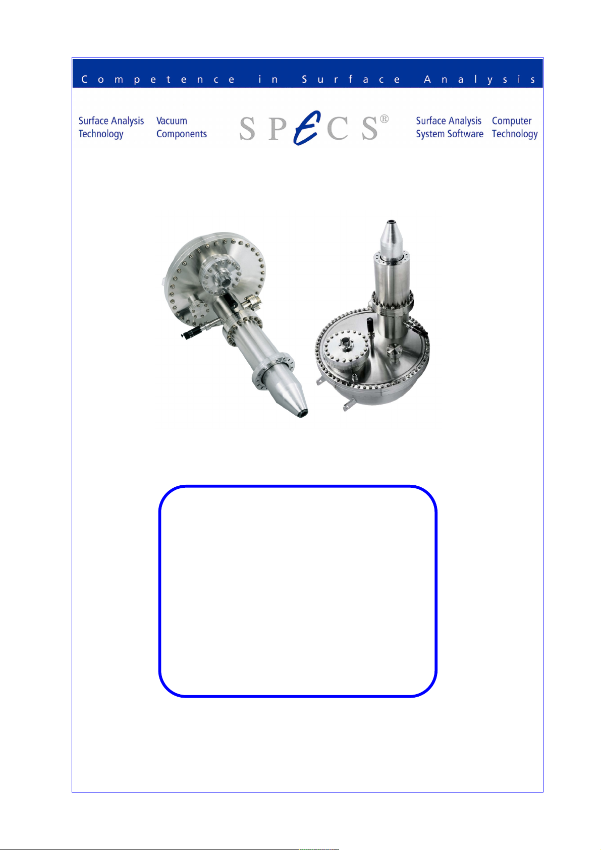
PHOIBOS
Hemispherical Energy
Analyzer Series
PHOIBOS 100 / PHOIBOS 150
3.1
Page 2

All rights reserved. No part of this manual may be reproduced
without the prior permission of SPECS GmbH.
User manual for the Hemispherical Energy Analyzer Series PHOIBOS 100/150.
Version 3.1 revised 19 November 2008.
SPECS order number for this manual: 78 000 101.
SPECS GmbH - Surface Analysis
and Computer Technology
Voltastrasse 5
13355 Berlin
GERMANY
PHONE:+49 (0)30 46 78 24 -0
FAX: +49(0)30 4 64 20 83
http://www.specs.de
PHOIBOS
Page 3

Chapter
T Table of Contents
1 Introduction 1
1.1 Overview .....................................................................................1
2 Components and
Connections 5
2.1 System Description, Package Contents .....................................5
2.2 Electrical Connections ................................................................6
3 Spectrometer 11
3.1 The Lens System ........................................................................12
3.2 Hemispherical Analyzer (HSA) .................................................18
3.3 Magnetic Shielding ...................................................................20
3.3.1 Magnetic Coupling for -Metal Chambersμ ...........................................21
3.3.2 Trim Coil .................................................................................................21
3.4 Slit Orbit Mechanism ................................................................22
3.5 Single and Multichannel Detector (SCD) / (MCD) ...................25
3.5.1 Principles of Detection ..........................................................................25
3.5.2 Coherence of Epass and Step ................................................................26
3.5.3 Electron Multiplication ..........................................................................27
3.5.3.1 Extended CEM ..................................................................................29
3.5.3.2 Linearity of the CEM’s .....................................................................30
3.5.4 Conversion Energy .................................................................................32
3.5.5 Spectrometer Voltage U0 ......................................................................33
3.6 Work Function ..........................................................................34
4 Installation 37
4.1 Unpacking .................................................................................37
4.2 Mounting the Detector ............................................................37
4.3 Achieve the Maximum Lifetime of a Channel Electron Multi -
plier 39
PHOIBOS
Page 4

Table of Contents
4.4 Alignment .................................................................................40
4.4.1 Analyzer Alignment ...............................................................................40
4.5 Vacuum Installation ..................................................................41
4.6 Baking Out ................................................................................43
4.7 Electronic Units Installation .....................................................44
4.8 SpecsLab Hardware and Software Installation .......................44
5 Unit Operation 47
5.1 First Operation ..........................................................................47
5.2 Quick Start .................................................................................47
5.3 Detailed Operation ...................................................................48
5.3.1 Slit Setting ..............................................................................................48
5.3.2 Detector Operation ...............................................................................48
5.3.3 Functional Test .......................................................................................49
5.3.3.1 XPS (AES/UPS) Operation .................................................................49
5.3.3.2 ISS Operation ...................................................................................50
6 Troubleshooting 51
6.1 Short Circuits .............................................................................51
6.2 Possible Problems .....................................................................51
7 Calibration 57
7.1 Complete Calibration Procedure .............................................58
7.2 Recalibrate the DAC Precision .................................................59
7.3 MCD Calibration .......................................................................60
7.4 Work Function Calibration with UPS ......................................61
7.5 Work Function Calibration with XPS .......................................62
7.6 Offset Calibration with UPS .....................................................62
7.7 Gain Calibration with XPS ........................................................64
8 Analyzer Checks 65
8.1 Independence of Peak Position with Pass Energy ..................65
8.2 Energy Scale Tests with XPS .....................................................66
8.2.1 Check Kinetic Energy Scale ....................................................................66
8.2.2 Check Peak Position ...............................................................................66
8.3 Specification Check ...................................................................67
8.3.1 Survey Spectrum of Silver ......................................................................67
8.3.2 Intensity and Resolution ........................................................................68
8.4 Connection Check of the Analyzer Electrodes .......................70
8.4.1 Capacitance Check for Electrodes .........................................................71
8.4.2 Check the Cable Contacts ......................................................................71
8.5 Check all analyzer voltages ......................................................73
PHOIBOS
Page 5

Table of Contents
9 Deflector Settings 75
9.1 Preamplifier ...............................................................................75
9.1.1 Discriminator ..........................................................................................75
9.1.2 Amplifier Check .....................................................................................76
9.2 Detector Voltage ......................................................................76
9.3 Noise ..........................................................................................77
9.3.1 Suppress a Noisy Channel ......................................................................77
9.3.2 Switch off Certain Channels ..................................................................77
9.3.2.1 Mask example for MCD9 .................................................................78
9.3.2.2 Mask example for MCD5 .................................................................79
10 Spare Parts 81
10.1 Cu Gasket ..................................................................................81
10.2 Multiplier ...................................................................................81
10.2.1 Channeltron Handling and Storage ......................................................81
10.2.1.1 Handling of the Multiplier ..............................................................81
10.2.1.2 Operation of the Multiplier ............................................................82
10.2.1.3 Storage of the Multiplier ................................................................82
10.2.2 Change a Channeltron ..........................................................................82
10.2.2.1 Removing the Detector Flange .......................................................82
10.2.2.2 Replacing Channeltrons ..................................................................82
10.2.2.3 Mounting the Detector Flange .......................................................83
PHOIBOS
Page 6

Table of Contents
PHOIBOS
Page 7
Chapter
1 Introduction
1.1 Overview
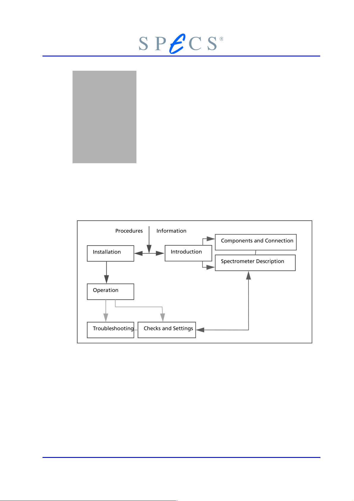
Chapters in this manual:
The SPECS PHOIBOS hemispherical electrostatic energy analyzer allows recording of energy spectra for negative particles (electrons) and positive particles (ions) in the kinetic
energy range from 0 eV to 3.5 keV.
The PHOIBOS series of hemispherical analyzers are hemispherical deflectors available in
two sizes, 100mm or 150 mm mean radii. The input lens is designed to accommodate a
wide range of applications.
The analyzer can be equipped with single-channel and optional multichannel detectors;
a 5-channel detector for the PHOIBOS 100 and a 9-channel detector for the PHOIBOS
150. The detection electronics incorporates a discriminator, preamplifier, counter and
PHOIBOS 1
Page 8

Introduction
bus interface. All parts are integrated into a single, compact RF-shielded aluminum
case. The detection electronics are supplied together with the analyzer control unit.
PHOIBOS analyzers provide the detection of electron and ion energies between 0 and
3500 eV with minimum step widths of 7 meV. For ultra high energy resolution applications the unit can be operated in a 400 V or a 40 V range with extremely low ripple.
Step widths down to 80μV are possible in the lowest voltage range.
A multi-element, two-stage transfer lens can be operated in several different modes for
angular and spatially resolved studies. All lens modes can be set electronically. A Slit-Orbit mechanism and a Multi-Mode Lens make the sampling area of the analyzer and the
acceptance angle area of the lens selectable. Thus the analyzer allows spatially resolved
measurements down to a diameter of 100 μm as well as large area investigations associated with different lens acceptance angles.
All units are completely controlled by SPECS software. Operation of the software will be
described in a separate manual.
Typical uses of the PHOIBOS analyzer include photoelectron spectroscopy (XPS, SSXPS,
UPS), Auger electron spectroscopy (AES, SAM) and ion scattering spectroscopy (ISS). The
PHOIBOS analyzer is bakeable up to 200°C after removal of the detector electronics and
the connection for the lens supply.
2 PHOIBOS
Page 9
Overview
Safety Information
Before any electric or electronic operations please consult
“SPECS Safety Instructions” and follow them strictly.
Some adjustments that have to be performed in this manual are dangerous. At each
point these are indicated by a warning label:
Warning!
Tests to be performed on the electronic unit are with its cover removed. Hazardous
voltages are present. Only trained, qualified personnel are allowed to perform this
task.
PHOIBOS 3
Page 10

Introduction
4 PHOIBOS
Page 11

Chapter
2 Components and
Connections
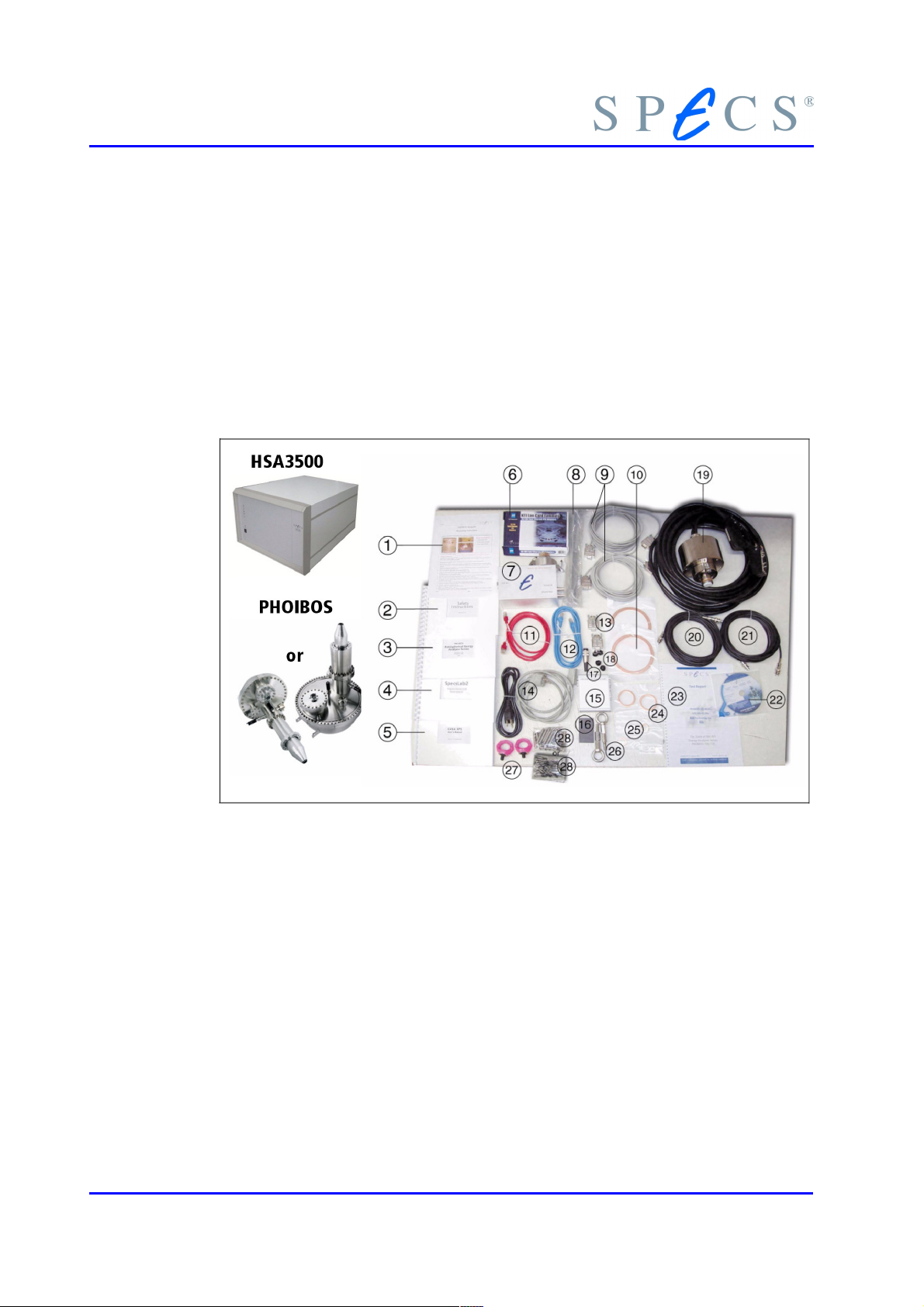
2.1 System Description, Package Contents
The contents of your system should include the components listed below. Please refer
to figure 1 for photos of these.
● PHOIBOS analyzer
The PHOIBOS analyzer consists of the following internal parts:
▪ analyzer housing,
▪ internal μ-metal shielding,
▪ lens system,
▪ hemispherical analyzer,
▪ multichannel (MCD) or single detector (SCD)
▪ Slit Orbit mechanism.
● HSA3500 power supply for PHOIBOS analyzer (fully remote controlled).
● and the following additional parts:
1. Mounting instructions
2. Manual Safety Instructions
3. Manual PHOIBOS
4. Manual SpecsLab2
5. Manual CasaXPS
6. Second network card (Fast Ethernet PCI Adaptor)
7. Detector electronics PCU 300
8. Handle for power supply HSA3500
9. 2 x RS232 cables - CAN bus cable
10. Pair of DN100CF copper gaskets
11. Cross over cable 2m
12. Ethernet cable TP 2m
13. 2 x terminator plugs CAN bus
14. Power line cables
15. EC10 CAN-Ethernet-Adapter (section on page )
16. Magnet holder for EC10 Adapter
17. Vacuum interlock plug (shorten pin1-pin2)
18. HSA3500 cabinet feet
PHOIBOS 5
Page 12
Components and Connections
19. Analyzer box with filter unit (cube or cylinder shape) , fixed cable
20. SHV-cable ChannelBase
21. SHV-cable ChannelHV
22. SpecsLab2 Installation CD
23. Specification (Test Report)
24. Pair of DN40CF copper gaskets
25. Pair of DN16CF copper gaskets
26. Two Lugs for analyzer lift
27. Two Lugs for analyzer support (only PHOIBOS 150
28. Screws for lens flange
(screws and nuts for PHOIBOS 100 and bolts and nuts for PHOIBOS 150)
Figure 1: Package Contents
2.2 Electrical Connections
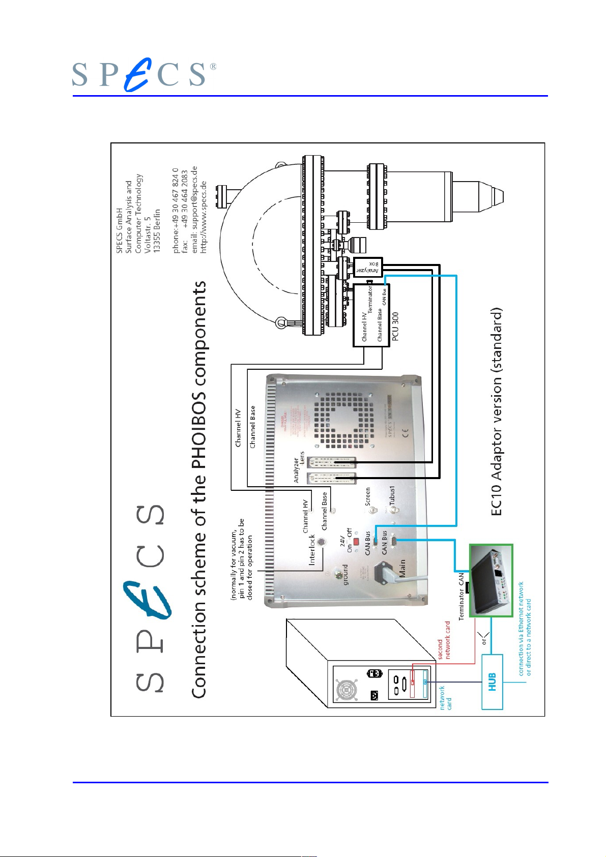
The electrical connection diagram is shown in figure 2, page 7. The connection to the
analyzer and the detector are supplied by two multi-pin vacuum feedthroughs that are
designed for high voltages up to 5 kV. More detailed descriptions are given in section
and section 8.4 .
All devices must be switched off before connecting or removing cables.
6 PHOIBOS
Page 13
Electrical Connections
Figure 2: Connection Scheme
PHOIBOS 7
Page 14
Components and Connections
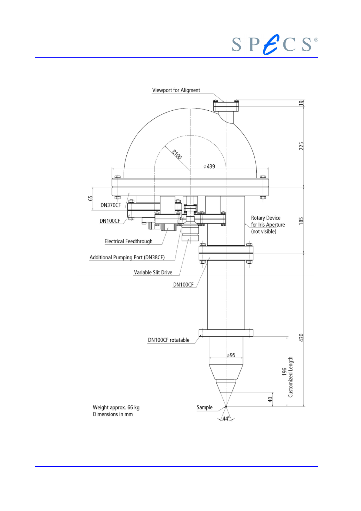
Figure 3: Analyzer Housing (PHOIBOS100)
8 PHOIBOS
Page 15
Electrical Connections
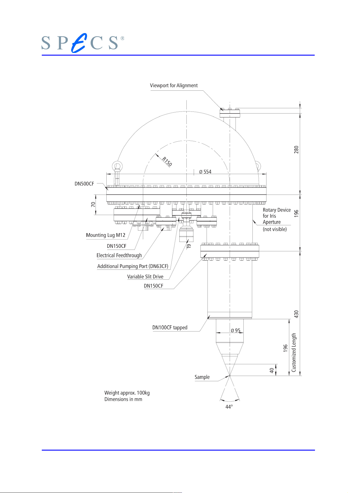
Figure 4: Analyzer Housing (PHOIBOS150)
PHOIBOS 9
Page 16
Components and Connections
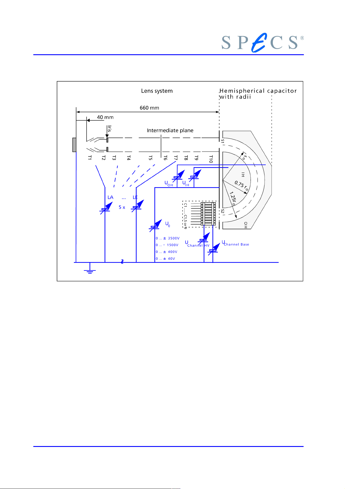
Figure 5: Analyzer Main Components and Voltage Principle
U0 main retardation voltage numerically equal to
- kinetic energy (Ekin) +pass energy (Ep) + workfunction (WF)
UChannel HV / Base anode / cathode potential for the channeltrons
UHV - UBase detector voltage
UChannelBase - U0 conversion voltage
LA..LE lens potentials
IH, OH inner / outer hemisphere
T1 to T10: electrodes of the multi mode transfer lens
S1: hemispherical capacitor entrance slit
S2: hemispherical capacitor exit plane
IH: inner hemisphere
OH: outer hemisphere
ro: nominal capacitor radius (100 or 150 mm)
C1 to C9: discrete collection, single / multichannel detector
(1, 5 or 9 channels)
single channel detection (SCD), multi channel detection (MCD)
10 PHOIBOS
Page 17

Chapter
3 Spectrometer
The PHOIBOS spectrometer consists of a vacuum housing and four major internal components, which are shown in figures 3 - 5. All the parts must be contained within an Ultra High Vacuum (UHV) environment, as particles emitted from the sample surface can
collide with the gas molecules changing their energy and momentum.
The internal components are:
● input lens system for receiving charged particles;
● 180° hemispherical analyzer (HSA) with 100 / 150 mm nominal radius for per-
forming spectroscopic energy measurements;
● detector assembly for single particle detection;
● Slit Orbit mechanism with an external rotary feedthrough.
● Iris aperture with an external rotary feedthrough
The excitation source is dependent upon the technique to be used, but is commonly xrays or other photons, electrons or ions. Before the particles pass into the hemispherical
analyzer, they first pass through an electron lens system and a slit. Both the electron
lens system and the slits sizes (entrance and exit) have an effect on the energy spread
detected by the analyzer.
The input lens system (Figure 5: Analyzer Main Components and Voltage Principle page
10) includes ten lens tubes. For undisturbed image quality, the input lens system is gridfree. The lens stages define the analysis area and angular acceptance by imaging the
emitted particles onto the entrance slit of the analyzer. Particles passing through the
lenses are focused onto the input slit S1 and are retarded in the lens for subsequent energy analysis. In addition the lens stages define the acceptance angles and area for a
given magnification entrance slit (see table 2 on page 16).
The lens system may be operated in several different modes for angular and spatially
resolved studies to adapt the analyzer to different tasks. All lens modes can be set electronically.
For small spot analysis a lateral resolution down to 100 m is available using the Highμ
Magnification Mode and the special Iris aperture. In the various Magnification Modes,
PHOIBOS 11
Page 18

Spectrometer
angle-resolving is accomplished with an Iris aperture in the diffraction plane of the lens
system. using the Iris the angular resolution can be continously adjusted while keeping
the acceptance area on the sample constant.
The transmission modes are optimized for high transmission at different spot sizes of
the source. The lateral resolution is worsened and the acceptance area normally not
defined by the lens.
In the angular dispersive modes, the emission angle distribution is imaged instead of
the real image. All lateral resolution is lost, but instead the emission angle information
is easily available. These modes are intended for UPS band mapping, Fermi surface mapping or similar experiments.
In the hemispherical capacitor, the particles passing through the entrance slit S1 are focused onto the capacitor output plane S2. The radial position of the slit image in plane
S2 depends on the kinetic energy of the particles in the capacitor. Particles on the central trajectory possess the nominal pass energy. They are focused to the central radial
position at the exit plane S2. Particles with higher kinetic energy are focused further
outside, and particles with lower energy are focused further inside in plane S2. This offers the possibility of multichannel detection, with simultaneous recording of an energy
band around the nominal pass energy. Particles passing through the capacitor output
plane S2 are accelerated onto the detector system C. With the multichannel detector,
each channel is connected to a separate preamplifier mounted outside the vacuum. The
preamplifiers are read out by the Multi Channel Detector (MCD) counter interface of
the SPECS data acquisition software.
3.1 The Lens System
The multi-element, two-stage transfer lens was designed to yield ultimate transmission
and well-defined optical properties. It may be operated in several different modes for
angular and spatially resolved studies to adapt the analyzer to different tasks. All lens
modes can be set electronically.
A lens system with the variable Slit Orbit mechanism is necessary to
● image the sample plane on the HSA entrance plane
● define the analyzed sample area and the accepted solid angle on a sample,
● accelerate / decelerate the particles with the observed energy to the pass en-
ergy.
The standard working distance of 40 mm and the 44° conical shape of the front part of
the lens provide optimum access to the sample for all kinds of excitation sources. At the
lens stage, the particles emerging from the sample S are imaged onto the entrance slit
S1, with the sample being in the focal plane of the lens system, i.e. 40 mm in front of
the first lens electrode T1. Inside the lens stage the particles pass through an intermediate image before they are focused onto the input slit S1 of the hemispherical capacitor
(figure 5). At S1 the particles have been retarded by the energy difference between the
nominal particle kinetic energy E
and the nominal pass energy E
kin
pass
.
12 PHOIBOS
Page 19
The Lens System
DS=D1/M
If S1 has the dimension D1, then by theory the imaged area of the sample has the
dimension DS with
(1)
The magnification of the lens stage is selectable (see table 2 on page 16). The magnification is changed electrically by connecting appropriate voltages to the lens electrodes.
The voltages are a function of the spectrometer voltage U0 which is nominally equal to
Ekin - Epass + workfunction. Ekin is negative for electrons and positive for ions.
The PHOIBOS system can operate in a Fixed Retarding Ratio (FRR) or in a Fixed Analyzer
Transmission (FAT) mode. In FAT mode the applied voltage to the hemispheres is
defined by equation 3 on page 18. In the FRR mode, the pass energy is given by Epass =
Ekin /R, with the retardation ratio R.
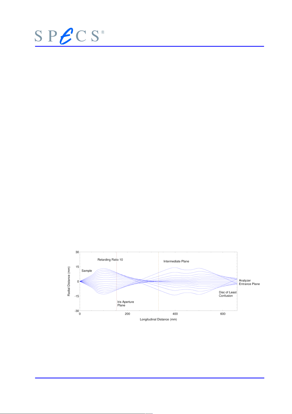
The actual size of the analyzer sampling area DS is, in principle, given by equation 1.
However, due to spherical aberration of the input lens, the image in the plane of the
entrance slit is diffused. The degree of diffusion increases for a fixed magnification with
the input lens acceptance angle. This means that the observed area in the focal planes
of the input lens system is smeared out with increasing angle, resulting in larger
sampling dimensions than given by equation 1. Thus the lens acceptance angle is selectable by the magnification modes, keeping the spherical aberration at a well known, acceptable value.
A second reason for confining lens acceptance angles are angle-resolved measurements,
e.g. in tilt experiments or angle resolved photoemission investigations. Confining the
lens acceptance angle is also essential in ISS, as the kinetic energy in ISS depends on the
scattering angle, and thus peak broadening or double peaks appear when the lens acceptance angles are too large.
Figure 6: High Point Transmission Mode
PHOIBOS 13
Page 20
Spectrometer
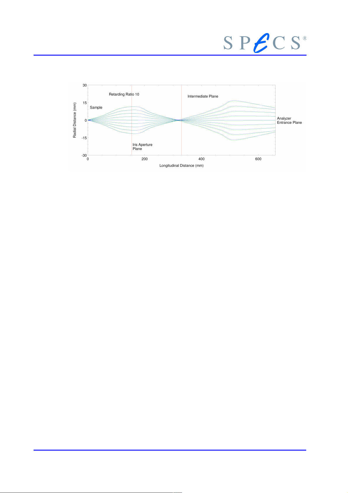
Figure 7: Medium Area Mode
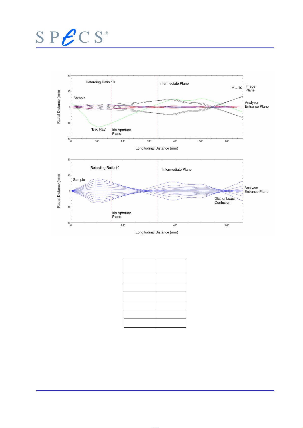
High Magnification is (see Figure 8: High Magnification Mode page 15) particularly suitable for spatially resolved studies. The image plane of the sample is in coincidence with
the entrance plane of the analyzer. The user can define the acceptance area of the analyzer with the entrance slit. As the trajectories of electrons emitted from the sample are
influenced by electrical fields around the sample, T1 has a fixed potential, which is set
to ground, after switching on the power supply. Due to lens aberrations, rays entering
the lens far away of the lens axis at larger angles could find a path to the analyzer entrance. With an Iris aperture these “bad rays” can be eliminated. Furthermore the Iris
Aperture can be used to continuously adjust the angular acceptance of the analyzer.
For small spot analysis a lateral resolution down to 100 μm is available using the High
Magnification Mode and the Iris aperture.
The magnification modes were optimized to allow very large acceptance angles for
high transmission from point sources (Point Transmission Modes). In these modes angular resolution is accomplished with the Iris aperture in the diffraction plane of the lens
system. Using thie Iris, the angular resolution can be continuously adjusted between ±1°
and ±9° while keeping the acceptance area on the sample constant. The rays close to
the lens axis (paraxial rays) are focused at the Gaussian focus. Rays entering the lens at
a larger angle are converged more strongly. The disc of minimum confusion is where
the envelope of emergent rays has its smallest diameter. Slight under-focusing of the
lens displaces the disk of least confusion to the image plane. Thereby a higher angular
acceptance is achieved but the spatial resolution is worsened. This makes the Point
Transmission Modes most suitable for AES, ISS and synchrotron studies. As with the
High Magnification Modes, the Iris Aperture can be used to continuously adjust the angular acceptance.
14 PHOIBOS
Page 21
The Lens System
Figure 8: High Magnification Mode
Acceptance
Angle
±1° 3.5mm
±2° 7mm
±3° 10mm
±4° 13mm
±5° 15.5mm
±6° 17.5mm
Iris
Diameter
Table 1: Acceptance Angle vs. Iris Diameter for a Point Source
In the novel, angle-resolved Medium Area mode, electrons leaving the sample within a
given angular range are focused onto the same location of the analyzer entrance independent of their position on the sample. The angular modes allow the user to optimize
the angular resolution down to ±0.05 ° with the Slit-Orbit mechanism. With a 2-D detection system high angular resolution can be achieved in the dispersion direction of
PHOIBOS 15
Page 22
Spectrometer
the analyzer without restricting the acceptance angle; this mode is the ideal choice for
angular dependent studies.
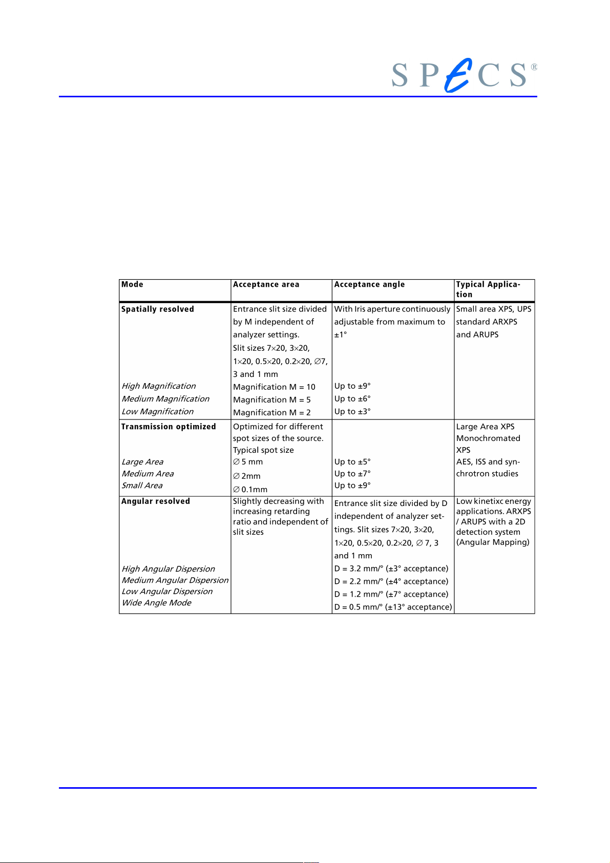
Magnification and angular aperture are selectable with PHOIBOS. There are many different combinations available. The lens settings can be combined with the different
possible slit combinations, resulting in “lens settings” x “number of slits” possible combinations. The analyzer sampling areas and input lens acceptance angles for these combinations is given in table 2. The table shows the standard lens modes of operations.
Additional acceleration modes for low kinetic energy applications are also available
(HighMagnification2 and SmallArea2).
Table 2: Overview of the Lens Modes
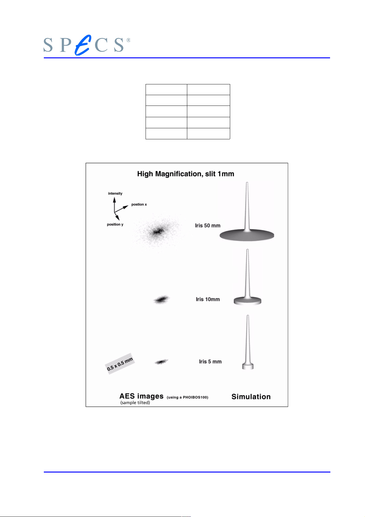
For small spot analysis the iris aperture may be used to sharpen up the analysis area.
The optimum settings for the iris aperture depends on the slit size and the desired quality of the analysis area. The intensity-position function for the analyzer is a Gaussianlike function, but with higher intensities in the tail regions (see figure 9). Using the iris
aperture these intensities can be suppressed. The analysis area was defined to include
typically between 90 - 99% of the total photoelectron signal.
16 PHOIBOS
Page 23
Slit Size Iris Diameter
7 x 20 mm 30 – 40 mm
The Lens System
∅ 7
∅ 3
∅ 1
20 – 30 mm
10 – 20 mm
2.5 – 10 mm
Table 3: Recommended Iris Values for Spatially Resolved Measurements
Figure 9: Typical Intensity-Position Profile with Iris Aperture
The low tail intensity forms a disc. Its integrated intensity can achieve the same order of
magnitude as the intensity in the peak. Using the iris aperture these intensities can be
PHOIBOS 17
Page 24
Spectrometer
R
0
=
R
inner
R
out
2
=150mm
E
pass
=−qk∇
V
k
=
R
innerRout
2R0
R
out
−
R
inner
=0.9375
E
an
E
pass
=
S
2
R
0
2
4
suppressed.
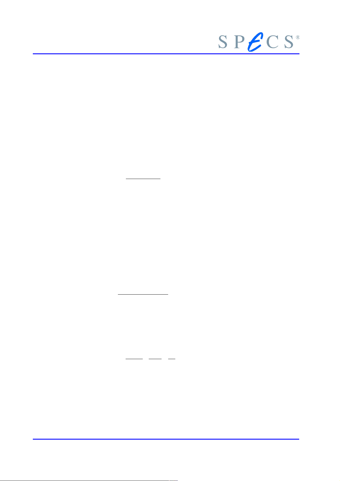
3.2 Hemispherical Analyzer (HSA)
The PHOIBOS Hemispherical Analyzer (HSA) with a mean radius R
measures the energy of charged particles. Charged particles entering the HSA through
the entrance slit S1 are deflected into elliptical trajectories by the radial electrical field
between the inner hemisphere R
PHOIBOS hemispheres are 1.25 R0 and 0.75 R0, respectively. The entrance slit S1 and exit
plane S2, are centered on the mean radius R0:
For a fixed electrical field gradient, only particles with kinetic energies in a certain energy interval are able to pass through the full deflection angle from the entrance slit S1
to the exit plane S2. Particles with higher kinetic energy approach the outer hemisphere, whereas particles with lower kinetic energy are deflected toward the inner
hemisphere. Those particles, which enter the HSA normal to S1 and move through the
hemispheres on the central circular trajectory, have the nominal pass energy Epass:
where q is the charge of the particle, ∆V is the potential difference Vout - Vin applied to
the hemispheres, k is the calibration constant,
and the outer hemisphere R
IN
(2)
(3)
(100mm/150mm)
0
. The radii of the
OUT
(4)
These particles reach S2 at the nominal radial position R0. If the HSA accepts the half
angle α in the dispersion direction, the HSA resolution or FWHM (full width at half maximum) of the transmitted line ∆Ean is given by
(5)
where S=(S1+ S2)/2. This value is a constant of the analyzer.
There are additional contributions to the line width observed in the spectrum. For
photo-emission lines, the main additional contributions are:
● inherent line width of the atomic level ∆Elevel (e.g. O 1s, C 1s),
18 PHOIBOS
Page 25

Hemispherical Analyzer (HSA)
FWHM
total
=
E
an
2
E
level
2
E
photo
2
1/2
=
E
HM
Mg K
=0.8
eV
FWHM
extreme
=0.44
eV
I
~
E
anSAS
=
E
an
0A0
E
pass
E
kin
~
E
pass
2
E
kin
● natural line width of the characteristic radiation used for excitation ∆Ephoto (e.g.
Mg, Kα, Al Kα).
The observed total FWHMtotal is given by the convolution of the single FWHMs, e.g for
gaussian line widths.
(6)
FWHMtotal is usually specified using a sputter-cleaned silver sample and recording the
Ag 3d5/2 level, after linear background subtraction. For Mg Kα excitation, the resolution
at low HSA pass energies for the Ag 3d5/2 level is found to be
(7)
In most practical work, a resolution of 0.9 eV is usually sufficient for high resolution investigations. For higher instrumental resolution, it is possible to use monochromatized
X-radiation for excitation, e.g. mainly monochromatized Al Kα radiation. For monochromatized Al Kα radiation and for the Ag 3d5/2 level, the extreme resolution is found
to be
(8)
To obtain the extreme resolution of 0.44 eV, the FWHM of the X-ray has to be heavily
restricted, by utilizing only a small part of the X-ray monochromator spot area (due to
the energy dispersion across the spot area), at the expense of a strong loss in intensity.
In practice, a resolution of 0.65 eV is usually sufficient for high resolution investigations
with monochromatized Al Kα excitation. For monochromatic radiation, FWHMtotal is
sometimes specified recording the Si 2p
level instead of the Ag 3d
3/2
level, which res-
5/2
ults in smaller values of FWHMextreme. due to the narrower inherent line width of the Si
2p level.
The integral signal intensity I of the measured particles (the area under the peak with a
background subtracted) is proportional to product of the accepted solid angle Ω
accepted sample area A
and the HSA resolution ∆E
S
:
an
, the
S
(9)
where Ω
and A0 are the values of the acceptances for the HSA. They are analyzer con-
0
stants. The equation results from Liouville’s theorem1.
The analyzer can be operated in two different modes:
a) Fixed Retarding Ratio (FRR), the retardation ratio R is defined as
1 For more information there are some excellent publications on analyzers. We recommend two of them:
K. D. Sevier, Low Energy Electron Spectrometry, Wiley-Interscience, 1972
D. Roy and D. Tremblay, Design of Electron Spectrometers, Rep. Prog. Phys. 53, 1621-1674,1990
PHOIBOS 19
Page 26

Spectrometer
R
=
E
kin
E
pass
I~E
kin
I
~
1
E
kin
I~E
pass
2
In this mode all particles are decelerated with this same fixed factor. Therefore the pass
energy is proportional to the kinetic energy. The intensity increases with kinetic energy:
while the energy resolution decreases.
(10)
(11)
b) Fixed Analyzer Transmission (FAT), Epass and ∆Ean in equation 5 are adjustable
constants. The signals of all particles, independent of the kinetic energy, are
measured with the same resolution and the intensity decreases with the kinetic
energy:
(12)
The two modes are generally possible for all kinds of measurements. There are some
applications where one of them is traditionally preferred. The FRR mode is mostly used
in AES, ISS and is convenient for the measurement of a survey spectrum. The FAT mode
is mainly used in XPS and UPS when detailed information is needed and the resolution
should not be dependent on the energy. If E
measured with different pass energies, it follows that
(13)
is kept constant and the same peak is
kin
3.3 Magnetic Shielding
Because charged particles are influenced by stray magnetic fields (including the earth’s
magnetic field), it is essential to cancel these fields within the enclosed volume of the
analyzer. The analyzer, the lens system and the detector are surrounded by one layer of
1.5 mm thick -metal to screen the external μ magnetic fields down to an uncritical level.
The shielding factor for the analyzer region is about 35. For ultimate performance the
analyzer and the lens system are constructed entirley from non-magnetic materials inside the -metal shieldingμ . (see also section 4.4 - Alignment on page 40)
20 PHOIBOS
Page 27
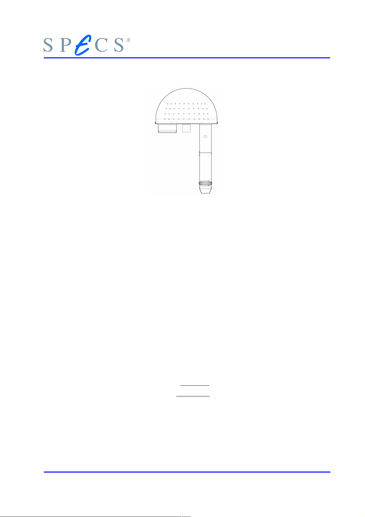
Figure 10: PHOIBOS µ-Metal Shielding
RG[m
]=3.37⋅
E
kin
[eV]
B[T
]
Magnetic Shielding
3.3.1 Magnetic Coupling for μ-Metal Chambers
A proper shielding of the front of the lens and the experiment chamber is also necessary, and to facilitate magnetic coupling to these parts, the PHOIBOS analyzer is delivered with a collar attached to the front of the lens shielding. The chamber shielding
needs good physical connection to the analyzer shielding, especially for slowly charged
particles. The insertion depth of the analyzer shielding has to be modified if the shielding is too far inside the chamber (normally by a non-magnetic lens protection cap added to the lens shielding). Please contact SPECS for advice regarding the -metal shieldμ -
ing.
3.3.2 Trim Coil
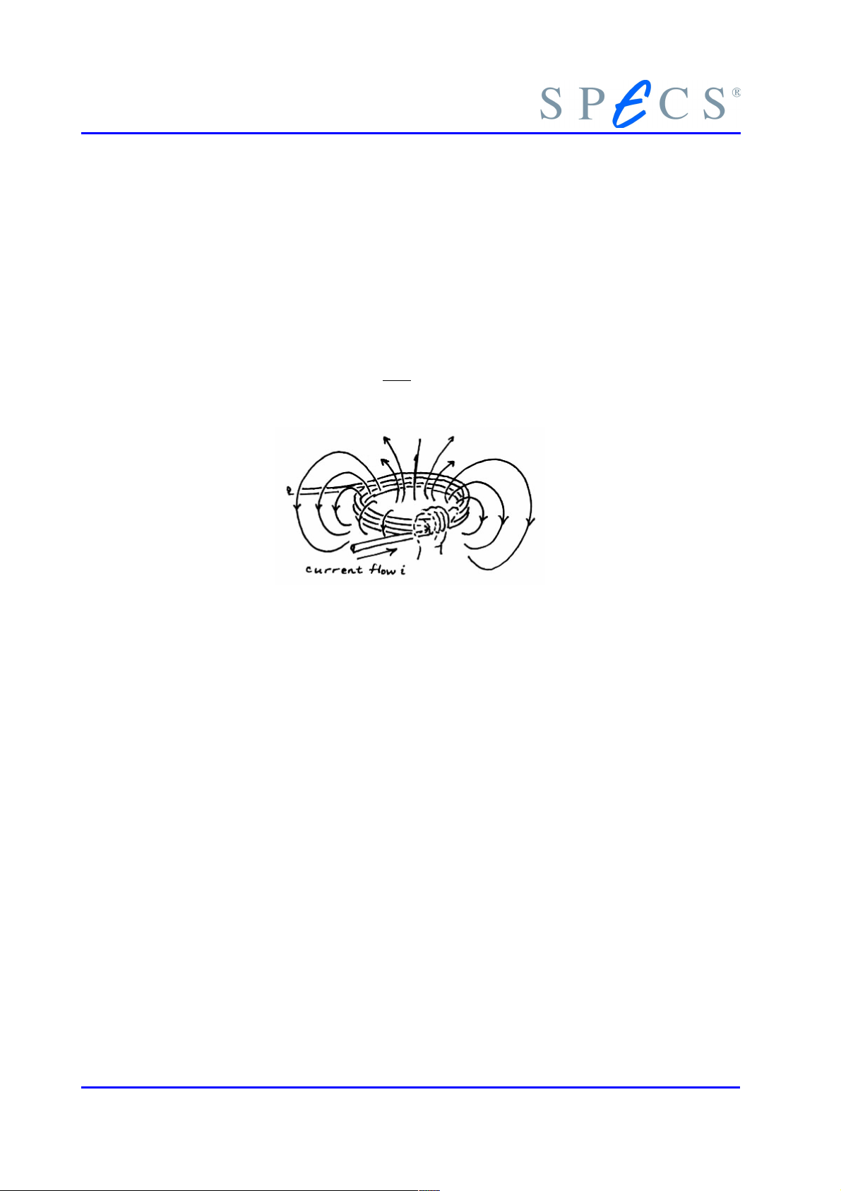
The PHOIBOS analyzer can be equipped with a trim coil around the outer hemisphere
of the analyzer. With a coil current |Icoil| < 150 mA the residual magnetic field component within the analyzer along the lens axis can be compensated. The magnitude and
the sign of the coil current depends on local terms.
The radius of gyration G for an electron with kinetic energy E
(14)
in a magnetic field B is
kin
At the center of a very short coil with coil current I, radius R and n windings the magnetic field is
PHOIBOS 21
Page 28
Spectrometer
B
=0⋅
n⋅I
2
R
(15)
Figure 11: Magnetic Field of the Trim Coil
For the PHOIBOS 150 analyzer B[μT] = 0.017 x I[mA] and for the PHOIBOS 100 analyzer
B[μT] = 0.026 x I[mA]. In the case of an earth magnetic field of about 50 μT with the
lens axis nearly parallel to the field one needs about 85 mA or -85 mA to compensate
the residual magnetic field within the hemispheres.
To find the optimal value for the current, the signal measured by the analyzer at low
pass energies (< 10 eV) should be maximized by changing the coil current. If the analyzer is equipped with a coil (short-circuit of PIN 12 to ground of the analyzer feedthrough) and the power supply HSA 3500 is equipped with a current module, the control software allows the setting of the coil current. In all programs the coil current setting can be found in the analyzer settings menu as an additional field.
3.4 Slit Orbit Mechanism
The slit orbit mechanism is used to manually change the entrance and exit apertures of
the analyzer. The mechanism positions an entrance and exit opening of the appropriate
size in the analyzer entrance and exit plane. The entrance beam is defined by a pair of
slits which are about 6 mm apart. The posterior slit lies in the entrance plane and
defines the analyzer energy resolution (see equation 5 on page 18), while the anterior
slit serves to match the angular spread for the analyzer. For a given energy resolution
and a given tolerated analysis area and acceptance angle, the largest possible slit
22 PHOIBOS
Page 29
Slit Orbit Mechanism
should be selected. This enables the highest possible count rate for these parameters
and thereby a short measurement time and a good signal-to-noise ratio.
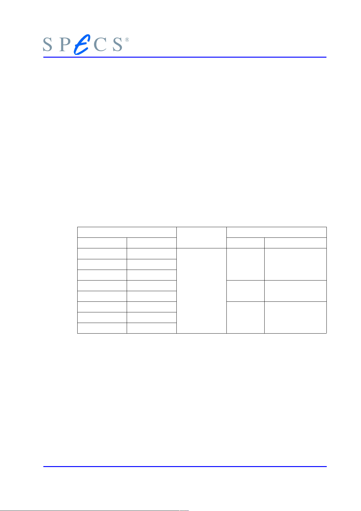
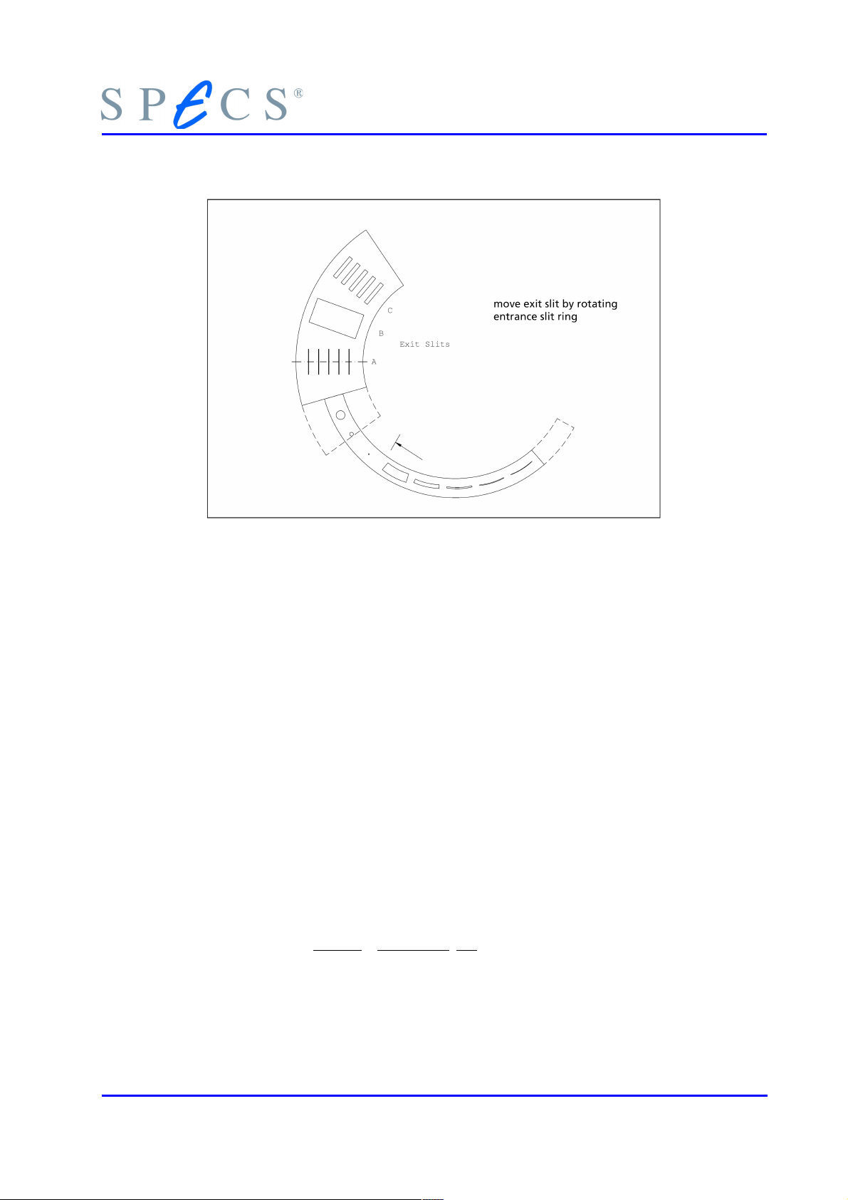
The entrance ring can be positioned directly by rotating the dial (see figure 13, “Entrance and exit slit rings (slit combination 4-B),” page 24).The exit ring on the other
hand is positioned indirectly by the use of the entrance ring (see Figure 13: Entrance
and Exit Slit Rings (Slit Combination 4-B) page 24). Through this arrangement one can
choose the entrance and exit slits independently using the same rotary drive.
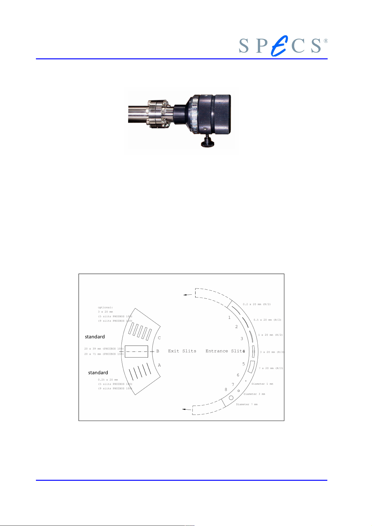
The PHOIBOS analyzers, beginning with release 5, have 8 entrance and either 2 exit slits
in the standard configuration or 3 upon request. The entrance slit positions are indicated by numbers (1-8) on the external rotary dial (see Figure 12: External Rotary Dial for
Positioning page 24). The exit slit positions are indicated by letters (A-B or A, B and C).
These indicators correspond to those which appear in the region settings of the analyzer control software SpecsLab 2. Whenever the entrance and exit aperture is changed
the positions must be entered in the region edit dialog. The arrangement of the slits
may be other than those shown in table 4 on page 23. The actual arrangement present
in an analyzer appears in the slit selection dialog of the control software delivered with
the analyzer.
Entrance S1 Exit E2
Slit Number Slit Size Slit Number Slit Size
1 0.2 x 20 mm Free choice of
2 0.5 x 20 mm
3 1 x 20 mm
4 3 x 20 mm B Open (for CEM each
5 7 x 20 mm
6 dia. 1 mm C 3 x 20 mm
7 dia. 3 mm
8 dia. 7 mm
each slit
combination
except
combination
8-A
and
1-C
A 0.25 x 20 mm
channel is 7x21 mm )
Table 4: Standard Slit Configuration
(May be different for your analyzer, please check the slit selection dialog of the SpecsLab2 software.)
PHOIBOS 23
Page 30
Spectrometer
The indicators on the rotary dial are used for positioning, but it must be taken into account that the rotary dial has some backlash. The correct slit positions are defined by
spring loaded indexing balls. Because of the rotary feedthroughs backlash, rotate it
beyond the desired position until the indexing ball snaps in.
Figure 12: External Rotary Dial for Positioning
After positioning the dial, jog it back and forth to ensure that the index is probably engaged. The correct positioning of the entrance slits can also be checked by looking
through the view port. In a configuration with two exit slits, the positioning of the exit
slit is not critical because of the end stops. In configurations with a third exit opening
please be aware that positioning of slit B can be tricky and require some practice. An
analyzer configured with two exit slits can be reconfigured on request.
Figure 13: Entrance and Exit Slit Rings (Slit Combination 4-B)
24 PHOIBOS
Page 31
Slit Orbit Mechanism
R−R
0
R
0
=
E
k
−
E
pass
E
pass
⋅
D
R
0
Figure 14: Exit Slit Selection
3.5 Single and Multichannel Detector (SCD) / (MCD)
The detector consists of the following parts:
● an arrangement of Channel Electron Multipliers (CEMs), 1 for SCD, 5 or 9 for
MCD, consisting of discrete collectors, specially screened against external HF-signals for maximum noise rejection;
● a multi-pin ceramic, high voltage vacuum feedthrough, specially designed for
low cross talk;
● SCD / MCD preamplifier;
3.5.1 Principles of Detection
Due to the spherical symmetry of the HSA, a one-to-one image of the circularly shaped
entrance slit with a radius of curvature R
electrons with a nominal pass energy E
energies within the HSA are concentric circles. In a first order approximation, the radial
image position R for electrons with kinetic energy E
exists in the exit plane for monochromatic
0
. The images of electrons possessing different
pass
is given by
k
(16)
where D is the has dispersion. The theoretical value for D is
PHOIBOS 25
Page 32

Spectrometer
D
=2⋅
R
0
E
k
=
R
D
⋅
E
pass
E
pass
=
D
R
⋅
E
k
The experimentally determined dispersion value can be slightly different, mainly due to
fringing fields at the edges of the analyzer.
Multichannel detection is performed by appropriately arranging 5 or 9 CEM‘s as collectors with 5 or 9 exit slits on concentric circles in the exit plane. The radial distance
between neighbouring exit slits ∆R is selected to meet the requirement of a constant
kinetic energy difference between neighbouring channels ∆E
N
preprocessed in the data acquisition unit.
By sweeping the spectrometer voltage U0, the electron path is moved across each collector channel step by step, and in this way each collector records a complete spectrum,
with a fixed energy offset between neighbouring channels. In principle, by sweeping
the spectrum once over the detector area, 5 or 9 parallel spectra are recorded simultaneously. As the kinetic energy En of the particles arriving at collector C
equation 16, the number of particles from each channel, belonging to the same kinetic
energy can simply be added, resulting in a total number of particles for each kinetic energy.
(17)
. The number of particles
k
arriving at each collector Cn is counted separately, and these numbers are stored and
n
is known from
n
3.5.2 Coherence of E
From the analyzer energy dispersion equation, the energy difference ∆Ek between
neighbouring channels at the distance ∆R one from another is
or
where D is the analyzer dispersion.
Especially in the FRR mode, where the pass energy changes throughout the spectrum
(and thus the energy difference between neighbouring channels) a calculation of the
detected energy of the particle is necessary. Therefore a software routine calculates the
particle number Nn in channel Cn at the nominal kinetic energy, by interpolation
between the numbers actually measured in channel Cn at the measuring energies
nearest below and nearest above the nominal energy.
This algorithm is unequivocal, because there is never more than one nominal energy
between two measured energy positions. Due to the interpolation routine, there is no
restriction on the energy step due to analyzer performance. Power supply performance
(DAC steps, etc.) limit the possible step widths and ranges. The software validates the
values to the nearest allowed values.
and Step
pass
(18)
(19)
26 PHOIBOS
Page 33
Single and Multichannel Detector (SCD) / (MCD)
3.5.3 Electron Multiplication
A Channel Electron Multiplier (channeltron or CEM) is a high gain device for detecting
energetic particles such as electrons and ions, or radiation. The CEM consists of a small,
curved glass tube. The inside wall is coated with a high resistance material. The resistive
material becomes a continuous dynode when a potential is applied between the ends
of the tube.
The impact of a charged particle results in secondary electrons that
are released from the CEM wall. These electrons are accelerated by
the high voltage connected to the CEM and release additional secondary electrons by impact with the wall further along in the CEM.
This effect is repeated successively, until finally an “electron cloud”
is present at the exit of the CEM.
The average number of electrons leaving the CEM assembly per incident particle is called the gain G. For single particle detection, the
gain has to be selected high enough to use the CEM‘s in “saturated”
operation, i.e. each incident particle releases an electron cloud at
the exit of the CEM arrangement whose charge is independent of
small changes in multiplier voltage. The saturated operation is necessary for sufficient noise rejection in single particle detection.
Usually the minimum gain for saturated operation is about 107, i.e.
an electron cloud of more than 107 electrons leaves the CEM.
The electron cloud emitted is accelerated onto the collector electrode of the CEM, and the charge pulse carried by the electron cloud
is detected as originating from one incident particle and counted in the preamplifier
channel.
One or a set of CEM‘s, is used in a special arrangement as an electron multiplying component for the PHOIBOS analyzers. The CEM‘s are all mounted in parallel as a unit on a
feedthrough flange. Particles passing the exit aperture are accelerated to an appropriate kinetic energy onto the CEM. The particle energy can be calculated as described in
section 3.5.4, "Conversion Energy" on page 32.
The Working Point of the CEM’s
The operating point for a channel electron multiplier (CEM) in the pulse counting mode
is usually determined by the point at which a plateau is reached in the count rate vs.
voltage characteristic. Within the plateau all electrons collected at the input of the CEM
give an electron pulse at the output, high enough to be detected by the electronics.
Additional increases in voltage raise the gain, but the count rate remains essentially
constant. Eventually, a point is reached where ion feedback becomes significant due to
very high gain, and the count rate increases rapidly. This will significantly reduce the
lifetime of the channeltron.
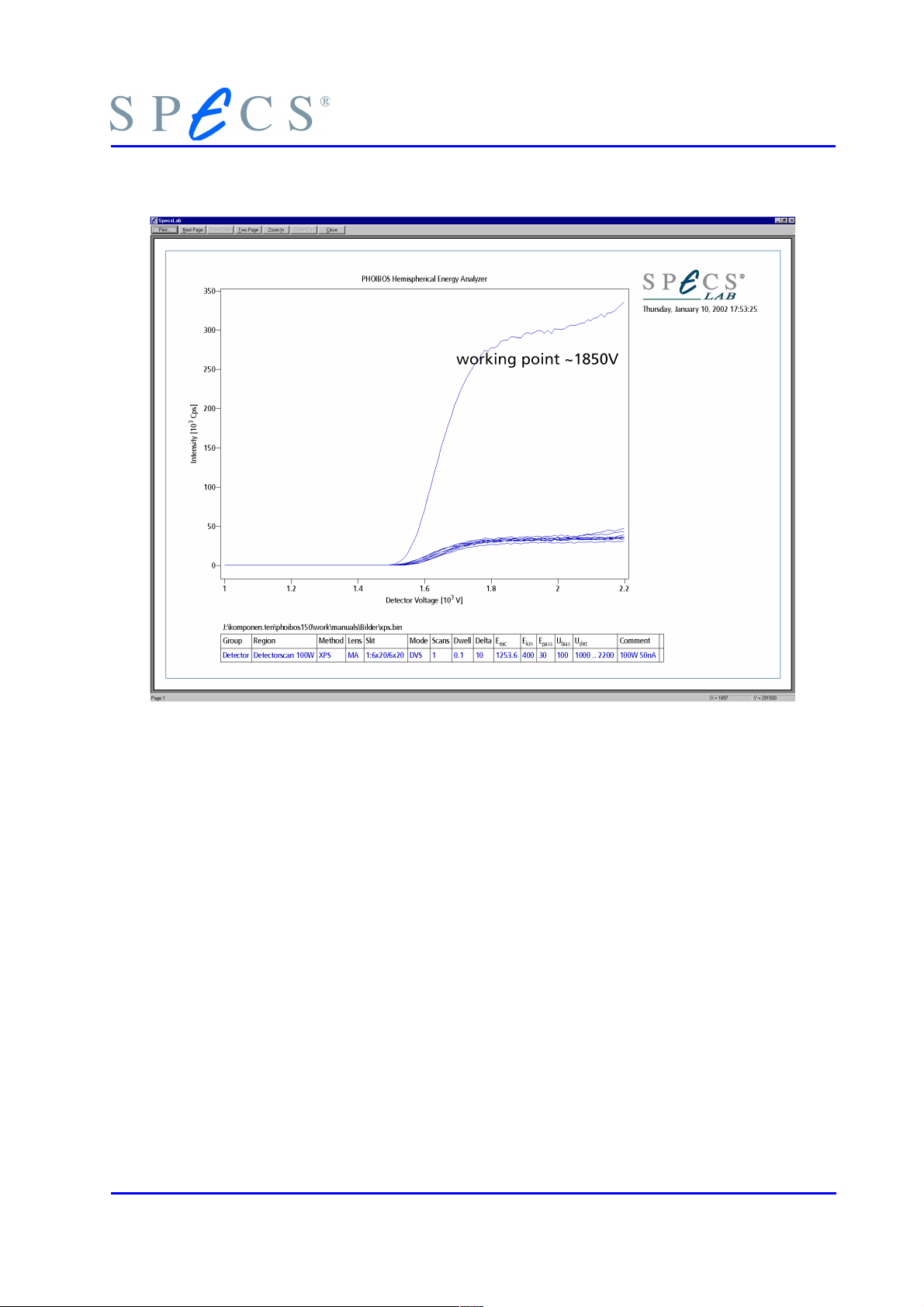
The Default Detector Voltage is normally given in the specification protocol of the analyzer and should be changed carefully. A detector scan gives the actual status of the
detector unit (see Figure 15: Detector Sweep, Count rate vs. Voltage on page 29). Note:
PHOIBOS 27
Page 34

Spectrometer
Please choose a moderate end value of the detector voltage scan to prevent rapid
aging of the detector!
The optimum operating point is about 50 - 100 V beyond the plateau of the curve (figure 15, page 29). As the multiplier ages, the knee moves to the right and the voltage
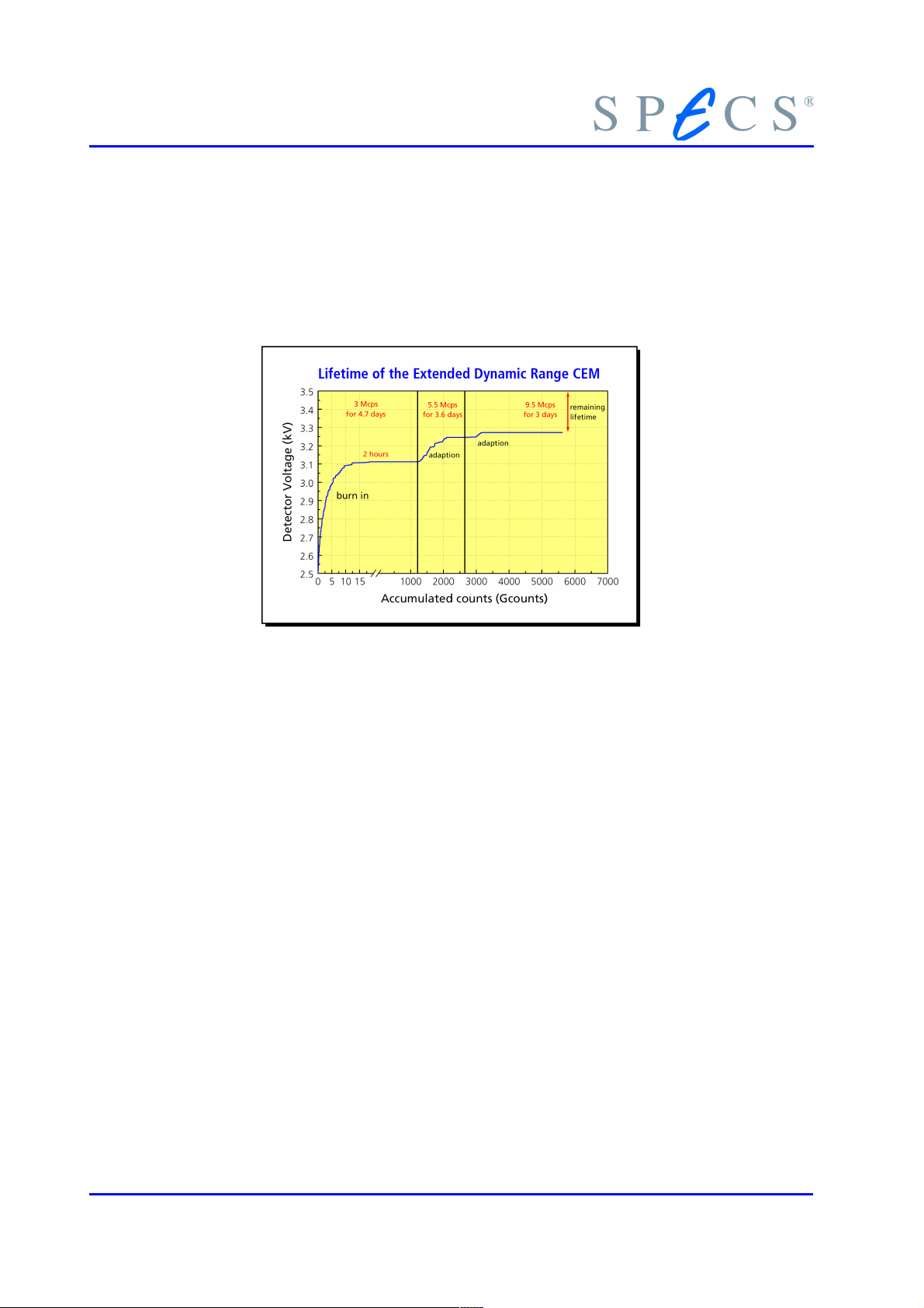
must be increased. In general, CEM lifetime (see figure 16, page 30) depends on the
number of counted electrons, thus it will vary as a function of specific application and
environment, but is typically on the order of about one year at 40 hours operation per
week.
For multi channel detection systems each channel should be displayed. The start value
for the detector voltage for counting depends on total number of accumulated counts
(see section 3.5.3.1 “Extended CEM” on page 29) and the threshold level of the
preamplifier. The sensitivity of the preamplifier channels can be varied using a discriminator threshold (the value is factory preset, recommended discriminator voltage see
section 9.1.1 “Discriminator” on page 79). Large differences between the channels can
be equalized by setting the threshold for the channels individually. These differences
may be caused by the varying sensitivities of the CEM’s. Pay attention to the detector
voltage value in the Specification Report sent with the analyzer.
The detector check should be done monthly (choose kinetic energy of 400eV).
28 PHOIBOS
Page 35
Single and Multichannel Detector (SCD) / (MCD)
Figure 15: Detector Sweep, Count rate vs. Voltage
The pulse output depends largely on the applied voltage and, in practice the gain is an
increasing function of the applied voltage until the gain reaches about 107: after which
point increasing the voltage further will cause the eventual breakdown of the CEM.
(With a properly configured oscilloscope, i.e. impedance 50 Ohm, the necessary pulse
height can be checked, usually between 2-10mV, see section 9.1.2 , "Amplifier Check"
on page 76.)
For the PHOIBOS analyzer, an input of one electron to the CEM produces an output
pulse that contains at least 107 electrons and lasts for approximately 10 nanoseconds.
3.5.3.1 Extended CEM
The standard detector systems of the PHOIBOS analyzer series are based on the extended range CEM. This device is a specially formed and treated glass tube which has the
effect of multiplying a single electron at the input to a pulse of around 10
the output. Because of the low resistance (about 50 ΜΩ) the extended range CEM’s are
suitable for extremely high count rates.
A voltage between 2.5 - 3.5 kV across the cone and the tail-end initiates the electron
multiplication. Electron multiplication is produced by the emissive layer along the inner
8
electrons at
PHOIBOS 29
Page 36
Spectrometer
N '=N
/1N
surface of the channel. The gain is governed by the detector voltage and the condition
of the emissive layer. The condition of this layer changes with usage and to compensate
for a drop in emissive quality of the surface, an increased detector voltage can be applied keeping the overall gain constant. If the detector voltage has reached the limit of
3.5 kV the CEM is at the end of its life and needs replacing.
Figure 16: Lifetime of the Extended Dynamic Range CEM
● While a CEM is not counting, residual gases in the system are adsorbed onto the
channel walls, which are kept clean by electron bombardment during operation.
● When initially running a new CEM it needs approximately 20 × 10
9
counts for
conditioning. Once properly conditioned, or “burned in”, the surface on the
semiconducting glass channel is quite stable.
● The test results suggested that accumulations to 5 × 10
12
counts and higher can
be expected without serious degradation.
● The extended range CEM’s are suitable for extremely high count rates without-
serious degradation.
3.5.3.2 Linearity of the CEM’s
Inadequate design may cause electron analyzers to show non-linear behavior. For an
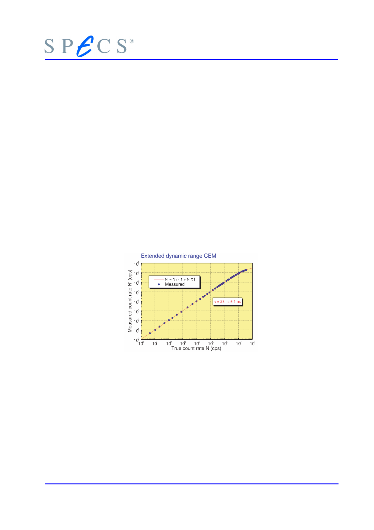
ideal counter with a non-extended dead time τ the measured count rate N’ and the
true count rate N are given by
(20)
With the PHOIBOS SCD analyzer the count rate as a function of the Auger electron
beam current has been measured using both the standard and extended dynamic range
CEMs. For a non-extended dead time counter the ratio N’1 / N’2 of two spectra N’1 and
N’2 (measured at two different beam currents A × I and I) the spectral ratio is given by
30 PHOIBOS
Page 37
Single and Multichannel Detector (SCD) / (MCD)
N '
1
/
N '
2
=A1−A××
N '
1
N '
1
/
N
1
=
N '
1
/
N '
2
×1−
N '
2
/
A
(21)
Therefore, from a spectral ratio plot the dead time can be determined. The detection
efficiency N’1 / N1 can now be calculated
(22)
Figure 17: Linearity Plot for the new Extended Range CEM
The count rate N’ was measured for different beam currents I. From the low count rate
region, the conversion factor c (N = c× I) can be calculated.
PHOIBOS 31
Page 38
Spectrometer
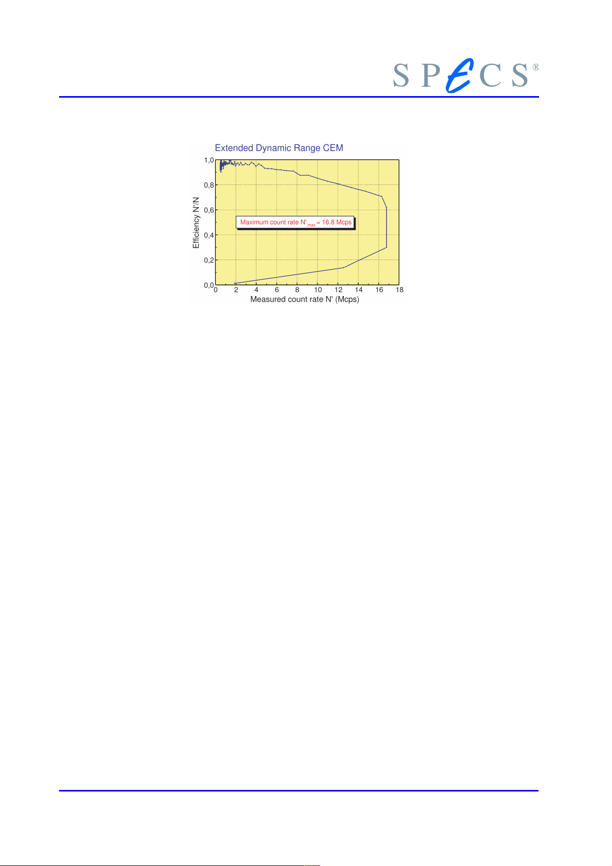
From a spectral ratio plot of two spectra measured at different beam currents the detector efficiency N’ / N was calculated. With increasing count rate the mean gain of the
pulse height distribution will decrease. For some critical value the distribution starts to
fall below the discriminator threshold.
Figure 18: Efficiency Plot for the new Extended Range CEM
Conclusions:
● The maximum (measured) count rate detectable is 5.6 Mcps per channel for the
standard CEMs and 16.8 Mcps for the extended range CEMs.
● The linearity and the non-extended dead time behavior for the standard CEMs
up to 1 Mcps and for the extended range CEMs up to 10 Mcps true count rate is
verified. Up to these count rates no significant deviation from linearity could be
observed with the PHOIBOS detection system (CEMs and PCU 300 detection
electronics).
● From pulse height distribution measurements the findings are that the mean
gain from the extended range CEMs is much less sensitive to increases in the
true count rate. This is the reason for the extended working range.
● The detector voltage required to operate the extended range type CEMs is 300
V higher than that for the standard CEMs.
● The high current AES survey spectrum shows the high count rate capability of
the PHOIBOS detection system with the extended dynamic range CEMs.
3.5.4 Conversion Energy
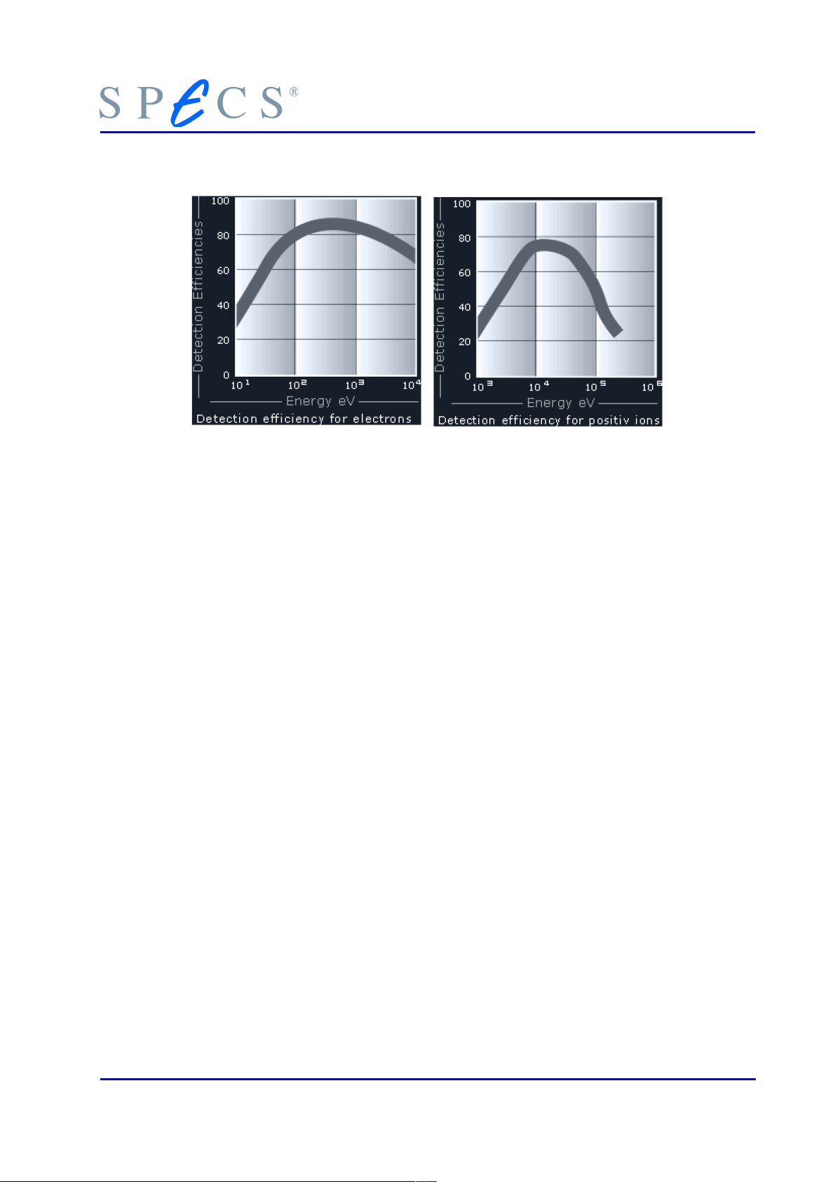
The detection efficiency of a CEM with respect to a particle is defined as the probability
of this particle or photon producing an output pulse. The detection efficiency curves for
electrons, positive ions and UV-light in figure 19 are based on published data and allow
an approximate estimation of the efficiency in the given energy and wavelength range.
32 PHOIBOS
Page 39
Single and Multichannel Detector (SCD) / (MCD)
E
conv
=−
q U
BIAS
E
pass
U
groundplate
=
E
kin
−
E
pass
−
WF/q
Figure 19: Detection Efficiency for Electrons and Ions
The BIAS voltage produced in the HSA3500 determines the conversion energy
(23)
of the charged particles impinging on the CEM. The proper conversion voltage has two
requirements which must be simultaneously fulfilled:
● the particles energy should be suitable for maximum yield of secondary electron
emission at the impact on the CEM wall. For electrons this is roughly in the energy range between 100 - 800 eV.
● For ions, the yield increases with the kinetic energy roughly up to 10 keV.
Standard settings are:
● for electrons: U
● for ions: U
BIAS
3.5.5 Spectrometer Voltage U
= + 90 V.
BIAS
= - 2000 V.
0
The main retardation voltage of the spectrometer U0 is numerically equal to the difference between kinetic energy (Ekin) and pass energy (Epass) + Work Function (WF). Because of the different polarity of the lens and hemisphere voltages in the different analyzer modes (XPS,AES,UPS or ISS) the value U0 is calculated by
(24)
The spectrometer voltage is applied on a groundplate and lens element 10 (Figure 5:
Analyzer Main Components and Voltage Principle page 10 and Figure 33: Schematics of
the 12-pin Analyzer Feedthrough page 72 as well as the comments in section , "" on
page .
Example:
WF=4.5 eV, Ekin =1000 eV, Ep= 100V
PHOIBOS 33
Page 40
Spectrometer
E
bin
=h−
E
kin
−
W f
sample
E
kin
W f
sample
=
E '
kin
W f
spectr
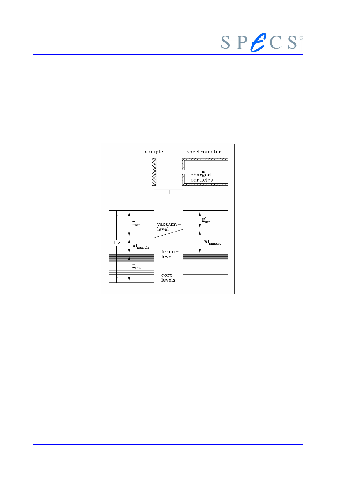
3.6 Work Function
The basic energetic properties are shown in figure 20 for the example of the measurement of photoelectrons.
● for electrons: U0 = - 895.5 V
● for ions: U0 = + 895.5 V
Figure 20: Energy Scheme – Photoelectron Spectroscopy
The spectrometer and the sample are connected to ensure that the Fermi-energies are
at the same reference level. The binding energy of the electrons is given by
(25)
The energy E′kin (see figure 20) is measured by the spectrometer and after calibrating
the work function of the spectrometer, the binding energy of the sample relative to the
Fermi level can be measured without knowing its work function because
(26)
Typical values of the analyzer work function are between 4 eV and 5 eV. The compensation is performed by addition through the software (see SpecsLab software manual).
For fine adjustment, use UPS mode measurement. Please check the analyzer settings in
34 PHOIBOS
Page 41

Work Function
the SpecsLab2 program. Adjust the desired voltage ranges separately (select the voltage
range in the analyzer settings before the measurement).
Please take note of section 7.4 “Work Function Calibration with UPS” on page 61.
PHOIBOS 35
Page 42

Page 43
Chapter
4 Installation
4.1 Unpacking
All analyzers and associated electronics are carefully packed before leaving the factory.
Carefully examine all packages for damage, especially the shock and tilt sensors inside
and outside the transport container. If damage is suspected please contact SPECS immediately for further instructions on what to do next.
The analyzer should remain in its protective packaging until it can be bolted directly
onto the system. Take great care when unpacking to prevent damage. Do not rest the
analyzer on the ceramic feedthroughs, lens or the viewport. Handle parts on the vacuum side of the flange seals using normal UHV protection, i.e. wear gloves and use clean
nonmagnetic tools.
The analyzer is evacuated. In order to avoid any damage, modest vacuum conditions
(10-3 mbar) have to be maintained. Please check vacuum conditions every three months
when storing the analyzer.
Please note the parts list in section 2.1 “System Description, Package Contents” on page
5.
4.2 Mounting the Detector
Caution!
Remove the three transportation locks before mounting the detector.
PHOIBOS 37
Page 44
Installation
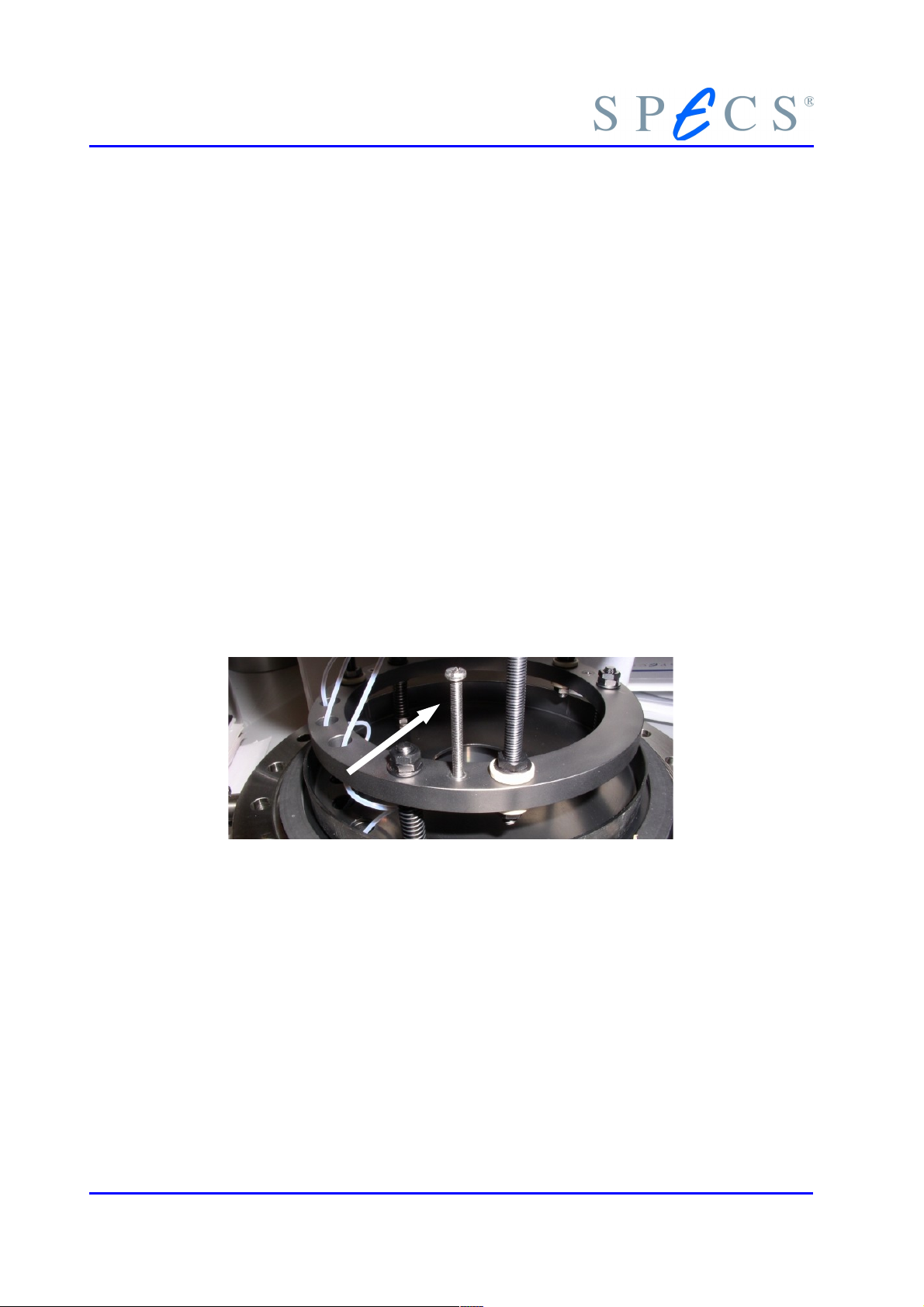
Figure 21: Removal of the Transportation Locks
Release the four M8 screws, vent the detector with N2, and pull it carefully out of the
storage housing. If one looks into the opened detector flange of the analyzer from the
bottom side, you can locate the 'alignment hole' for the detector. Align the pin at the
top of the detector assembly with the corresponding hole in the ground plate (see figure 21). Be sure that the detector is nearly parallel to the ground plate and push the detector carefully into its seat. While pressing the detector into its seat, make sure that
the distance between the two flanges is approx. 4 mm before you feel that the springs
are compressing. This will ensure that the ceramic spacers contact the ground plate.
Hold the detector in its position and tighten the flanges together with the M8 screws.
38 PHOIBOS
Page 45
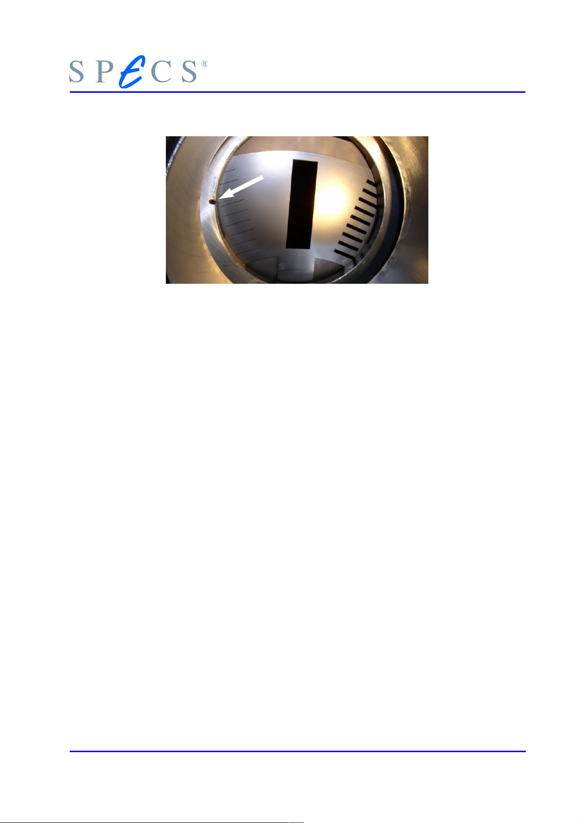
Figure 22: Corresponding Hole in the Ground Plate
Mounting the Detector
4.3 Achieve the Maximum Lifetime of a Channel Electron Multiplier
To achieve the maximum lifetime of a channel electron multiplier the rules listed below
should be strictly followed.
● After a bakeout, the analyzer needs 2-3 days to cool down. If channel electron
multipliers are operated at higher temperatures (> 60° C) they can suffer severe
damage. Some channel electron multipliers will lose gain and exhibit a
markedly higher detector plateau.The interior parts of the PHOIBOS will cool
down significantly slower than the housing. It is recommended to wait for a
complete cool down of the detector assembly; at least 2 days. Even if the analyzer housing is cold, any internal parts on insulators may still be too hot for
safe operation. It is imperative that all users are aware of the issue and take the
necessary precautions.
● During first use after bake out, rapid desorption of surface adsorbed gas will oc-
cur from the walls of the channel electron multipliers, so care should be taken
not to use the detector at full channel electron multiplier voltage and full intensity within the first few hours of operation. We recommend to increase the
detector voltage over a period of 1.5 hours up to the recommended value. Use
the SpecsLab mode Detector Voltage Scan and set start, end, step and dwell
time parameter for this procedure.
● During the first few days of operation of a new detector, it is recommended
that high output currents are avoided (i.e. inputs above 1 Mcps). Taking this initial burn-in precaution can prevent premature failure.
● Choose a moderate value of the detector voltage to prevent rapid ageing of the
detector. The optimum operating point is about 50 - 100 V beyond the plateau
of the intensity versus detector voltage sweep, not more.
PHOIBOS 39
Page 46

Installation
● Backstreaming from oil diffusion pumps or roughing pumps has to be avoided
at all costs. It is strictly recommended to use cold traps and molecular sieve traps
and maintain them according to manufacturers specifications.
● Channel electron multipliers can be degraded by exposure to various types of
hydrocarbon gases which raises the work function of the surface and hence
causing gain degradation. Operation in a clean vacuum environment of 5×10⁻⁸
mbar or better is a must in order to ensure the long-life characteristics of these
devices.
● Other gases containing F, S and Cl, which may decompose under electron bom-
bardment must not enter the detector area.
● Due to the hygroscopic nature of the doped lead glass, it is important that the
channel electron multipliers are not exposed to air for more than one day. Dry
nitrogen should be used to vent the system.
● High intensity sources like electron sources needs special care. Start with lowest
source strength and narrow slit settings to avoid possible degradation.
● Measurements at the secondary electron cut-off needs special care. Use low pass
energies (3- 5 eV) and small slit settings to avoid possible degradation.
4.4 Alignment
Non-shielded chambers need no special modification of the lens protection (analyzer
shielding).
For shielded chambers, the shielding needs a good physical connection to the analyzer
shielding, especially for slow (<100eV) charged particles. The insertion depth of the
analyzer shielding has to be modified if the shielding is too far inside the chamber (normally by a non-magnetic lens protection cap added to the lens shielding). Please contact SPECS in this case.
For XPS, the distance between the X-ray source and the sample should be minimized to
obtain maximum count rates. The distance between the sample and the lens T1 must be
fixed to the working distance (sample distance) of 40 mm (see also section 4.4 , "Alignment" on page 40). None of these three parts should be in physical contact with one
another.
The performance of the channeltron decreases with time when exposed to air. Try to
minimize the time between its installation and evacuation the system.
4.4.1 Analyzer Alignment
After mounting the analyzer on the chamber a check of the sample positioning via the
analyzer viewport should be done. Use the iris aperture to locate the real center position of the lens system in respect to the desired acceptance area on the sample. Please
contact SPECS if you see a visible offset between this two positions.
40 PHOIBOS
Page 47
Alignment
Note that the analyzer was adjusted to the mounting flange axis during specification.
4.5 Vacuum Installation
1. Open the transport box carefully.
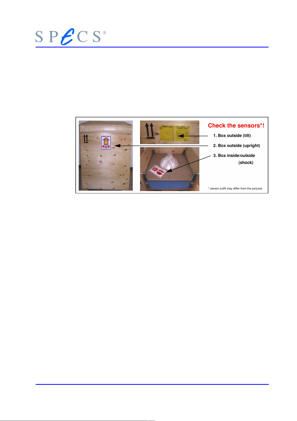
2. Check the shock and tilt sensors. If any sensor is discolored, please inform SPECS
immediately and await further instructions.
3. Remove the shipping frame.
4. Carefully lift the analyzer out of the box. Be aware of outstanding parts while
pulling out the analyzer. In particular the rotary feedthroughs are sensitive to
physical jostling / bumping / vibrations. Because of the analyzer weight of ~ 65
(PHOIBOS100) / 95 kg (PHOIBOS150).
PHOIBOS 41
Page 48
Installation
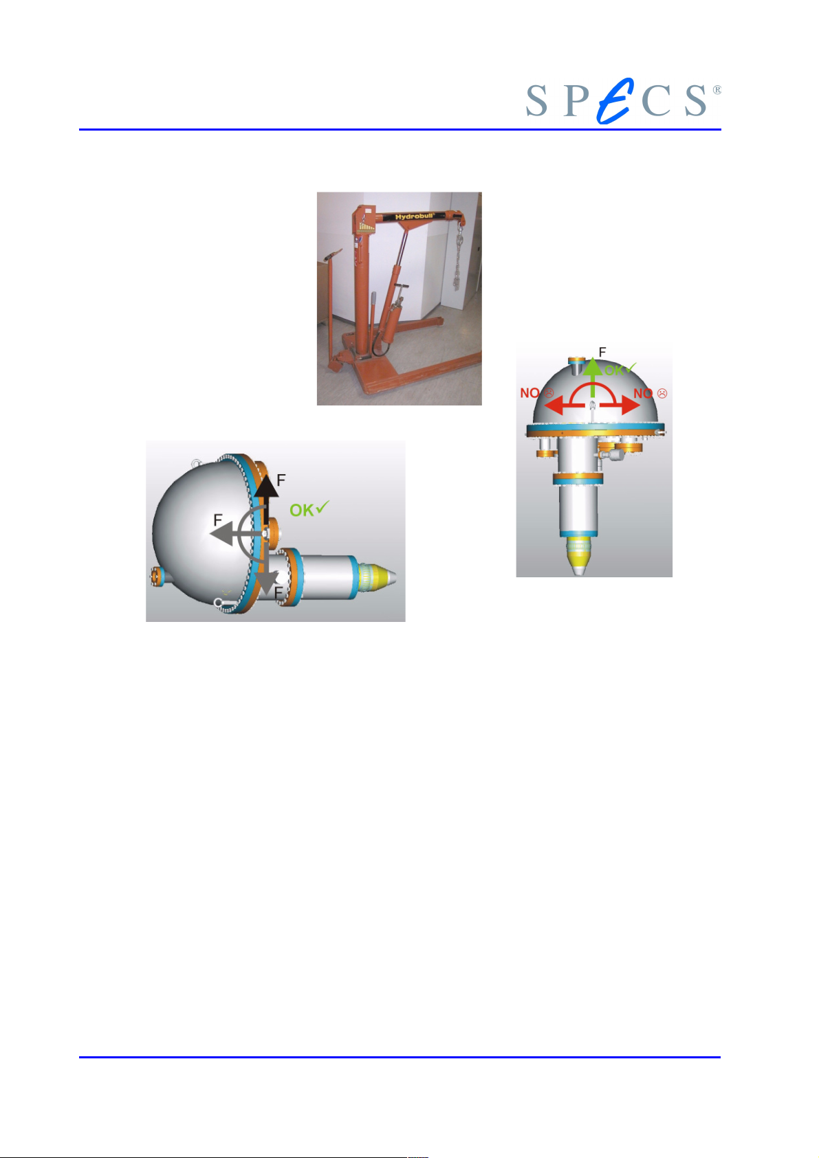
Specs recommends
using a hydraulic lift,
as in the photo to the
right.
When mounting vertically,
use the hooks as shown in
the picture above. Never
When mounting horizontally, use the
hooks as shown in the picture above.
use these for mounting
horizontally!
Figure 23: Mounting Tips
5. Keep the analyzer in a stable position, if possible keep the same orientation as
in the transport box (soft lie down is allowed).
6. The analyzer is evacuated. Vent via valve at the protection housing. SPECS recommends using a dry dust free venting gas like nitrogen to avoid particle or
water intrusion. Remove the lens protection housing from the analyzer mounting flange. Do not touch any vacuum parts without gloves.
7. Check the working distance of the analyzer (40mm between sample and the top
of the lens system -> insertion depth in your chamber).
8. Tighten the delivered stay bolts (PHOIBOS150) on the analyzer mounting flange
and prepare the necessary mounting parts (screws for PHOIBOS100, washers
and nuts).
9. Insert a new DN100CF copper gasket into the vacuum chamber flange.
10. Center the analyzer mounting flange above the vacuum chamber flange.
11. Introduce the lens system into the vacuum chamber flange very slowly. Do not
use any force.
12. During the introduction check all other components in the vacuum chamber for
possible physical damage. During the introduction check all other components
in the vacuum chamber because of possible physical damage. All rotary feed-
42 PHOIBOS
Page 49
Vacuum Installation
throughs are fixed with the locking screw during transport. Make sure to unlock
them before using the rotary feedthroughs and lock them again afterwards.
13. Adjust the analyzer at the vacuum chamber flange (Check section 4.4 “Alignment” on page 40).
14. Bolt the analyzer at the vacuum system flange with the delivered screws, washers and nuts.
15. For PHOIBOS150 and μ-metal chambers: Do not release the lifting gear until the
analyzer is supported by an additional supporting post!
16. Check the physical stability of the supporting post and the system frame and release the lifting gear.
17. Use the iris aperture and the analyzer view port to locate the real center position of the lens with respect to the desired acceptance area on the sample.
18. Evacuate the chamber to a pressure of below 10
-5
Pa (10-7 mbar) and bake out
(see section 4.6 “Baking Out” on page 43).
19. Check the vacuum before and after bakeout.
20. Connect the analyzer as described in the analyzer manual. (Figure 2: Connection Scheme page 7)
21. Before operating the analyzer wait for complete cool down (good thermal insulation inside the analyzer leads to a complete cool down time of about 2-3 days,
at least 2 days cool down is recommended).
4.6 Baking Out
The vacuum chamber has to be baked out to get good UHV in a reasonable time. The
temperature during the bake can be up to 200° C. A reference thermocouple for the
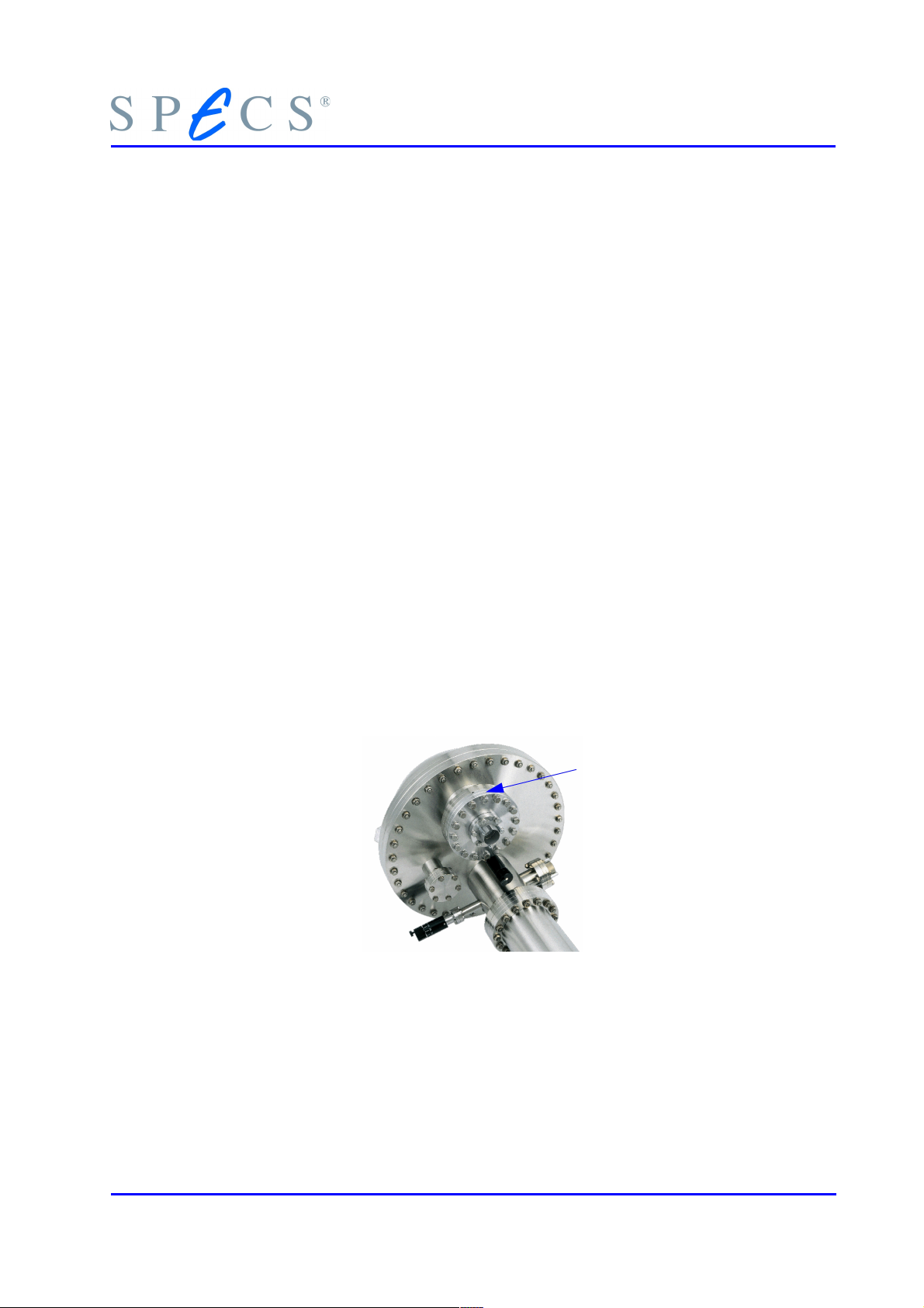
temperature measurement should be attached to the detector flange (figure 24)!
Thermocouple here
Figure 24: Detector Flange
Before baking out:
● Switch off the HSA3500 control unit.
● The analyzer box (fixed at the lens housing, see figure 4) should be removed as
well as,
● the detector box (preamplifier) with connection cables (Channel HV, Channel
Base, CAN)
PHOIBOS 43
Page 50

Installation
A bakeout time between 24 hours and 48 hours (first time) is recommended.
After a bakeout the analyzer needs two days to cool down. If channeltrons are operated at higher temperatures (> 340 K) they can suffer damage. Some channeltrons will
lose gain and exhibit a markedly higher detector plateau. The interior parts of the
PHOIBOS will cool down significantly slower than the housing. It is recommended to
wait for a complete cool down of the detector assembly; approximately 2-3 days. Even
if the analyzer housing just feels warm, any internal parts seated on isolators may still
be too hot for safe operation. It is imperative that all users be informed of this issue
and take the necessary precautions.
The multiplier will degas at first operation after bakeout, so care should be taken not
to use the detector at full multiplier voltage and full intensity within the first few hours
after bakeout. We recommend increasing the detector voltage over a period of 1.5
hours for the first use and over a period of 10 min for subsequent times after bakeout.
(Use the SpecsLab mode Detector Sweep and set start, end, step and dwell time parameter for this procedure.)
4.7 Electronic Units Installation
The electronic units have to be installed into a 19”-cabinet rack. Good air circulation
within the cabinet must be ensured. For wiring of the electronics follow figure 2 (page
7).
Note the following:
1. Connect all units to the same power strip.
2. The power strip must be provided with a protecting device according to, and
meeting all safety regulations.
3. A grounding bar (copper, brass) with a minimum cross section of 6×6 mm2 has
to be installed inside the cabinet. The electronic unit has to be connected to this
grounding bar.
4. The grounding bar inside the cabinet has to be connected to the system (e.g. to
the analyzer housing) by a ground cable of a minimum cross section of 10 mm2.
The connections between analyzer, control unit and computer are described in section
2.2, “Electrical Connections” on page 6. All connections described above have to be
made before the initial operation of the system.
4.8 SpecsLab Hardware and Software Installation
Read the instructions (e.g. section 2.2 , "Electrical Connections" on page 6 and SpecsLab2: Chapter 1: Installation) carefully before installing SpecsLab2 and evaluation program. You will find the manuals and other instructions in pdf-format on the installation
CD as well.
Please do not hesitate to contact SPECS for more detailed information.
[email protected] or
phone +49 (30) 467 824 - 0 or - 88)
44 PHOIBOS
Page 51

SpecsLab Hardware and Software Installation
PHOIBOS 45
Page 52

Page 53
Chapter
5 Unit Operation
5.1 First Operation
If the system is baked (see section 4.6, “Baking Out” on page 43) the vacuum should be
checked. The base pressure should be lower than 10-7 mbar (for more details please see
section 5.3.3, “Functional Test” on page 49). Check the electrical connections (see section 4.7, “Electronic Units Installation” on page 44).
After storage for a prolonged period please read the start-up procedure given for the
CEM after bake out in section 4.6 . Check the detector voltage given in the Specification
Report for your analyzer (spectra prints: column Udet) with the default detector
voltage (menu Analyzer/ Settings). A monthly check of this parameter (see figure 15,
page 29) is recommended.
5.2 Quick Start
1. Check vacuum conditions.
2. Check sample.
3. Switch on the analyzer supply HSA3500 (see section , on page ).
4. Start the acquisition program SpecsLab2.
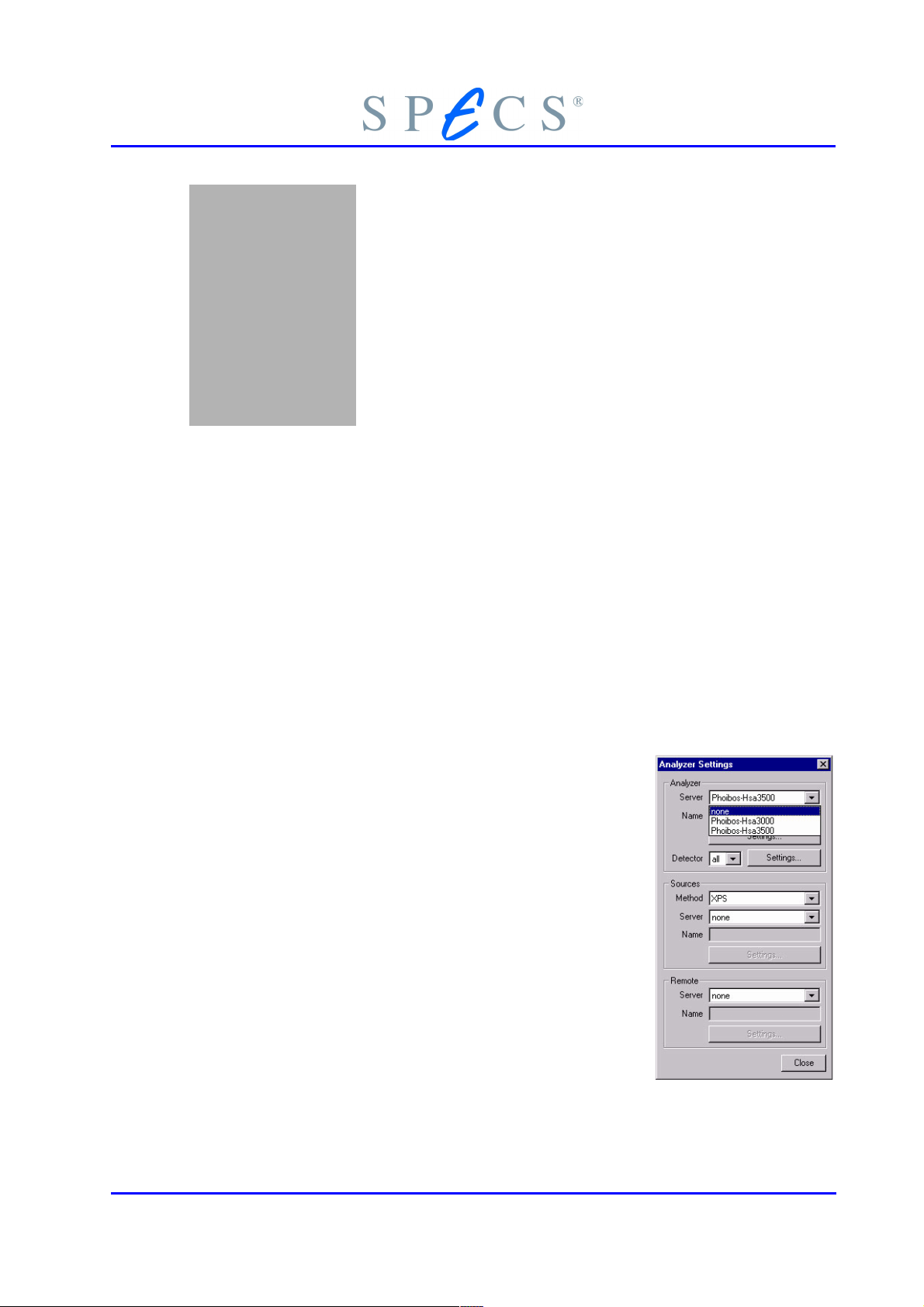
5. Select the HSA3500 control unit in the menu Analyzer / Settings
6. Switch on the excitation source.
7. Choose the desired slit combination (table 4 on
page 23). (A typical slit combination for standard
XPS and large samples ~10x10mm is 2:7x20mm /
2:open)
8. Set the Iris aperture to the desired diameter.
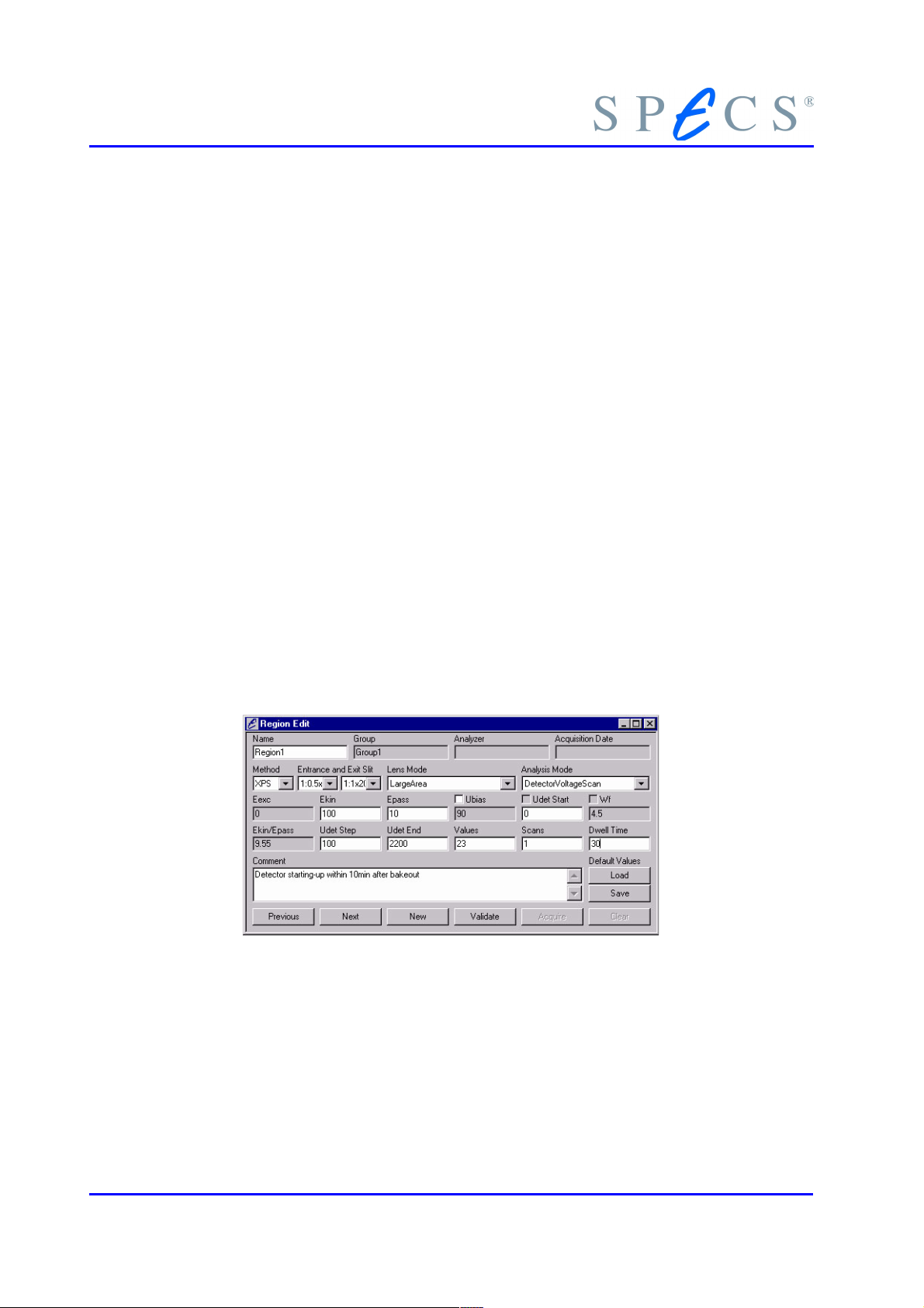
9. Set the scan parameter for the region (e.g. figure
31, page 68).
10. Press Validate and then Measure (window: Region
Edit).
11. Save the results.
12. Switch off the units.
PHOIBOS 47
Page 54
Unit Operation
5.3 Detailed Operation
5.3.1 Slit Setting
There are different settings available with the PHOIBOS Slit Orbit mechanism. To understand the possible slit combination for this analyzer please see section 3.4, “Slit Orbit
Mechanism” on page 22.
The optimum setting is reached when entrance slits are aligned along the lens axis, i.e.
when the particle number passing through the lens stages and impinging on the hemispherical capacitor entrance slit S1 is a maximum. There is also the correct position for
the exit slit S2. Usually there are only two exit slits, therefore physical stops in both directions means that this is also the correct exit slit position. In positioning the feedthrough (Figure 12: External Rotary Dial for Positioning page 24) to the slit locations,
the rotary dial is internally fixed near to the right value by a physical rest position.
Please check the marking at the rotary for the desired combination. Additionally, a
check via the viewport for alignment may help. A typical slit combination for standard
XPS and large samples (10x10mm) is 2:7x20mm / 2:open.
5.3.2 Detector Operation
For new multiplier (CEM) please read the start-up procedure given for the CEM after
bake out in section 4.6 . The normal procedure after bake out is increasing the detector
voltages in small steps (100V) over a period of 10 min without excitation.
Figure 25: Starting up the detector
Operating conditions:
● A dry-pumped or well-trapped/diffusion-pumped operating environment is de-
sirable. A poor vacuum environment can shorten CEM life or change the operating characteristics.
● A pressure of 1⋅10
high background noise due to ion feedback.
● Voltage should be applied to the MCD in small (100 - 200 V) steps.
-5
mbar or lower is preferred. Higher pressure can result in
48 PHOIBOS
Page 55
Detailed Operation
● For optimal lifetime, operate the detector at the minimum voltage necessary to
obtain an usable signal (see section 3.5.3, “Electron Multiplication” on page 27).
● Microchannel plates and Channeltron detectors can be degraded by exposure to
various types of hydrocarbon materials which raise the work function of the surface, causing gain degradation.
● If channeltrons are operated at higher temperatures (> 340 K) they can suffer
damage. Some channeltrons will lose gain and exhibit a markedly higher detector plateau.
5.3.3 Functional Test
5.3.3.1 XPS (AES/UPS) Operation
To begin, the detector unit should have already been baked out. A silver sample with a
size not smaller than 5×14 mm2 should have been transferred into the vacuum chamber. The sample has to be cleaned by sputtering. The base pressure should be lower
than 10-7 mbar (10-5 Pa) to avoid a damage to the detector by sparks. For special reasons, e.g. for depth profiling with noble gas ions, operation up to 10-6 mbar (10-4 Pa) is
allowed.
Adjust the detector voltage to the value corresponding to the Specification Report of
the analyzer or check the actual value (see “The Working Point of the CEM’s” on page
27).
Measure a wide energy XPS spectrum scanning the kinetic energy of the particles from
200 to 1.5 keV, e.g. with an energy step of 500meV and in FixedAnalyzerTransmission
mode with pass energy of ~10-20.0 eV (Figure 31: XPS on Silver, Wide Scan (PHOIBOS
150 MCD9), page 67).
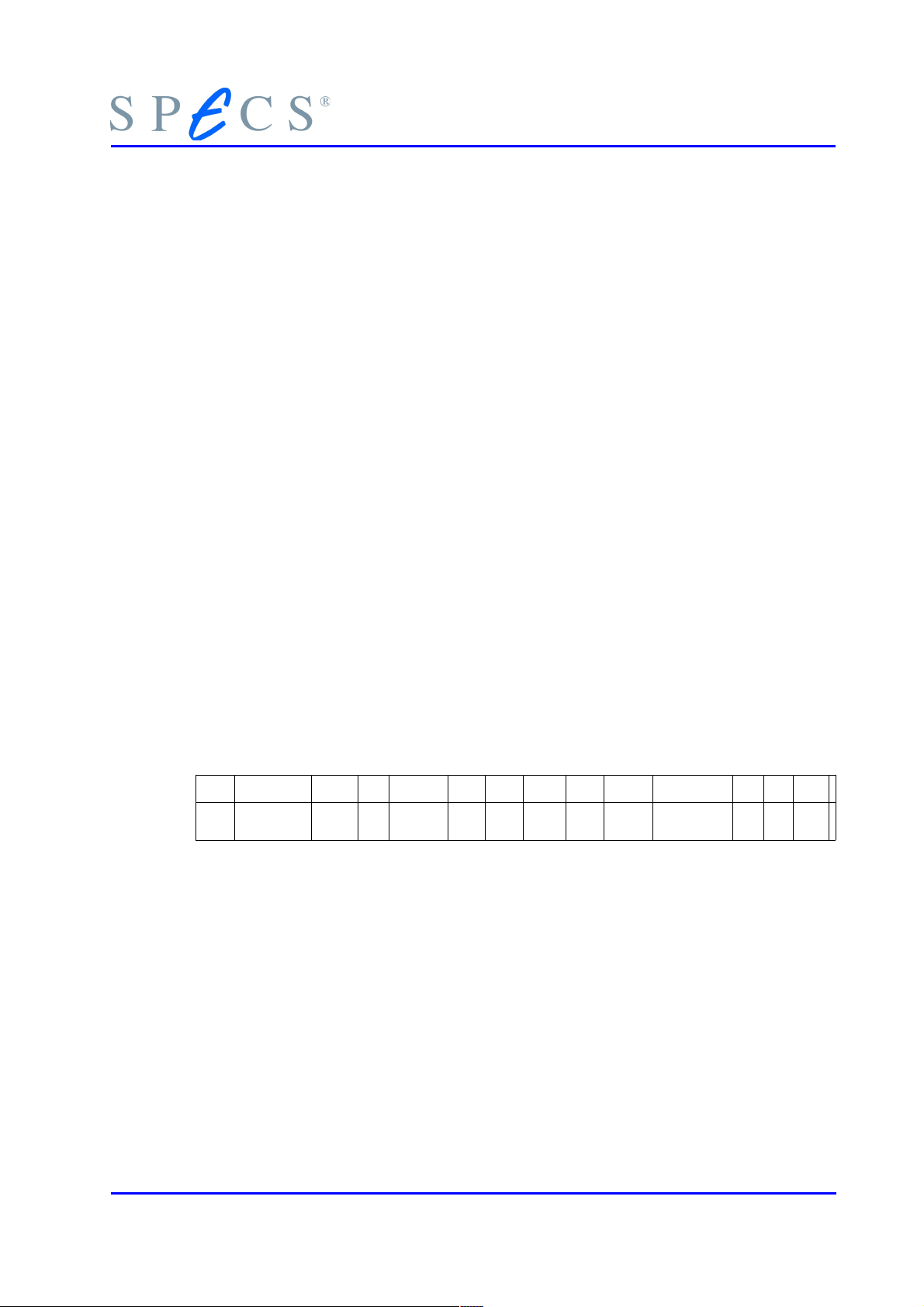
Group Region Method Lens Slit Mode Scans Dwell Delta E
300W Overview
300W, MA13
XPS MA 2:7x20
\2:open
FAT 1 0.01 0.3 1253.6 200 – 1267.4 13 90 1950
In a first rough test without careful adjustment one should get few 10
E
exc
kin
E
passUbiasUdet
4
cps at the Ag
3d5/2 peak using 100 W Mg Kα X-ray source power.
If not, check the photoemission sample current, which should be in the range of 25-40
nA for 100 W Mg Kα. Secondly, check the MCD voltage, and the discriminator level of
the MCD preamplifier. Also check whether the intensity of the C- and O-peaks are small
enough. Otherwise the sample should be sputtered once more.
PHOIBOS 49
Page 56
Unit Operation
5.3.3.2 ISS Operation
Please read these instructions carefully. Damage of channeltrons and amplifier are possible if the following is done incorrectly!
Set the detector voltage to the value corresponding to the Specification Report of the
analyzer or check the actual value (“The Working Point of the CEM’s” on page 27).
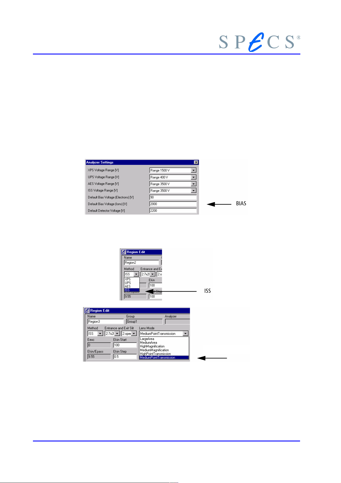
The conversion voltage (BIAS) in the Analyzer Settings window is default set to 2000
(see section 3.5.4, “Conversion Energy” on page 32).
The excitation source should be degassed and run under proper conditions to avoid
structures due to possible residual gas inside the sputter line.
Switch the method to ISS mode in SpecsLab.
Recommended lens mode: Point Transmission.
Point Transmission
Optimize the excitation source with typical sample current of less than 1 μA. Select the
FixedEnergies Analyzer Mode and choose a kinetic energy with measurable counts to
maximize intensity with the source deflection tools.
Check the function with an overview spectra.
50 PHOIBOS
Page 57

Chapter
6 Troubleshooting
In the section “Possible Problems” (below), a list of possible problems or anomalies and
suggestions for their removal is given. It is assumed that the system was calibrated
properly and was working according to specifications before one of the following problems occurred. Problems immediately after installation are mostly due to short circuits
caused by vibrations inside the analyzer while in transport and may be easily detected
by resistance measurements (section 6.1 “Short Circuits” on page 51). Please also note
the test described in chapter 8 - "Analyzer Checks" some spectra as well as the measured voltages for diagnostic purposes.
6.1 Short Circuits
Check the resistance of the pins on the HSA 12-pin (figure 33, page 72) and detector
(figure 34, page 73) feedthroughs to ground and to each other to rule out short circuits. It is especially important to check for a short circuit between the ground plate
and the cathode. The resistivity has to be infinite for all cases, except between the cathode and anode contacts of the CEM, Depending on the type and amount of your chan-
neltrons you will measure few MΩ internal resistance (50-300MΩ per channel or chan-
neltron. Note that the channeltrons are connected in parallel).
6.2 Possible Problems
The following problems may occur during operation of the analyzer system:
● no spectrum
● low intensity
● low resolution
● peaks shifted
● intensity fluctuations
● high background signal
● noisy spectrum
● incorrect area analyzed
● Slit Orbit problems
PHOIBOS 51
Page 58

Troubleshooting
An arrow ( →) after a statement indicates a separate troubleshooting procedure either
given here or in another manual.
Counter device or control unit defective contact SPECS
Possible Cause perform check, test, or troubleshooting
procedure no. →
X-Rays off check the X-ray source and the sample current
No voltage at detector check detector voltages
Spectrum definition incorrect check spectrum definition
Cable connection faulty check cable connections
Preamplifier box defective check preamp box section → 9.1.2
No energy sweep voltage check energy sweep section → and .
Spectrometer voltages incorrect check spectrometer voltages section →
Improper adjustment of slit orbit check proper adjustment section → 3.4
Table 5: No Spectrum
possible cause perform check, test, or troubleshooting
procedure no. →
X-ray intensity too low check whether on Ag sample photo current
≥0.2 - 0.3 nA/W
sample is dirty sputter until C and O peak in the spectrum
disappears
sample too rough remove roughness
incorrect analyzer - sample distance adjust distance to 40 mm
lens system and HSA out of focus check lens and HSA electrodes section → 8.4
and voltages section
CEM yield to low
conversion voltage too low
MCD preamplifier setting changed check preamp settings section → 3.5.3
some channels of the preamplifier unit
defective
magnetic fields Check whether the amount of the deviation
measure detector supply voltages →section
check conversion voltage →section 3.5.4
check operation of the preamplifier by use of
a separated channel mode of the software or
section → 9.1.2
depends on the energy of the measured electrons and on the pass energy (better by UPS).
Check the influence of an external permanent
magnet near the vacuum chamber.
physically incorrect adjustments like:
gridsdamaged, lenses misaligned,
52 PHOIBOS
Open analyzer system and check. Do this only
if all other kinds of faults can be excluded.
Page 59

spheres shifted, MCD shifted.
Possible Problems
improper adjustment of
Slit Orbit mechanism
check proper adjustment section 3.4
Table 6: Low Intensity
possible cause perform check, test, or troubleshooting
procedure no. →
chemical peak broadening sputter cleaning / replace anode
lateral inhomogeneous charging of the
sample
noise or/and ripple on the following
voltages: sample, spectrometer voltage
U0, detector voltage, electrode voltages
of the analyzer
magnetic fields in the region of the
spheres
preamplifier setting changed check preamp setting section → 3.5.3
lens system and HSA out of focus
detector supply voltage incorrect check detector supply voltages
use charge compensation by means of electron flood gun
ground sample and check hum and ripple
check the ground connection of all the power
supplies → section 4.7
measure magnetic field
check lens and HSA electrodes →
section 8.4 and voltages section
→section
carbon coating of HSA spheres
damaged
Humming and ripple on the following
parts: sample, spectrometer voltages,
multiplier voltage, lens voltage
open HSA and check do this only if all other checks are negative
ground sample, check humming and ripple
Table 7: Low Energy Resolution
possible cause perform check, test, or troubleshooting
procedure no. →
workfunction setting incorrect Check the work function setting, section 7.4 .
sample charging Check the sample ground connection. Use ex-
ternal electron flood gun to compensate for
the charging.
voltages of the HSA (inner and outer
sphere) are incorrect
zero point drift of the spectrometer
In similar spectra with different pass energies
the peaks are shifted. Check has voltages →
section 8.4
check zero point of HSA3500 →section
PHOIBOS 53
Page 60
Troubleshooting
Table 8: Peaks Shifted Equally
Table 9: Peaks Shifted Differently
voltage
possible cause perform check, test, or troubleshooting proced-
ure no. →
incorrect amplification factor
possible cause perform check, test, or troubleshooting proced-
check U0 HSA3500 section → 8.2 , section 8.1 ,
section
ure no. →
malfunction of counter board
one lens electrode not connected
malfunction of the energy sweep
→section 9.1.2
Run a spectrum with high speed. Perform a
crosstalk test with all lens tubes. section→
8.4.2
check the energy sweep →section , section
generator
Table 10: Intensity Fluctuations
possible cause perform check, test, or troubleshooting
procedure no. →
field emission at the exit slit of the HSA Background signal independent of Ekin with
DE=const, rises with small Epass - values and
increases in DE/E=const mode. Remove wireedge from the mesh at the exit slit.
sparks at the anode side of the CEM background signal is independent of Ekin in
DE/E=const mode and background to signal
ratio decreases with increasing of the pass
energy.
incorrect detector preamplifier
threshold
→ section 9.1.1
dark current at the isolation parts check spectra without excitation source 2nd:
disconnect the preamplifier and measure
again, see Chapter 9
Table 11: High Background Signal
possible cause perform check, test, or troubleshooting
54 PHOIBOS
Page 61

procedure no. →
Possible Problems
incorrect detector preamplifier
threshold
high noise of the primary source use a second excitation source,
electric interference monitor mains voltage, check ground connec-
section → 9.1.1 and section 3.5.3
tions section → 4.7
Table 12: Noisy Spectrum
possible cause perform check, test, or troubleshooting
procedure no. →
malfunction of lenses Check tubus voltages section , ‘Check all ana-
lyzer (HSA 3500) voltages” on page . The
voltage can be measured either at the 12 pin
feedthrough ( figure → 33 on page 72) or at
the rear of the HSA3500.
Note table 2 on page 16
improper adjustment of the
Slit Orbit mechanism
magnetic fields
check proper adjustment section → 3.4 ,
section 4.4
→section 3.3 and section 4.4
Table 13: Incorrect area was analyzed in all lens modes
PHOIBOS 55
Page 62

Page 63

Chapter
7 Calibration
Adjustment and calibration of the power supplies has been performed at the factory.
Normally no additional work is necessary after installation. The procedures described in
this chapter are only necessary for service and fine adjustment.
The typical accuracy of the energy scale depends on the voltage range used (Table , on
page ). For the 40V range the accuracy is about 3 meV and for the 3500V range about
100 mV without re-calibration. The drifts are due to different temperatures during calibration at the factory and work in the lab. Also, the workfunction of the analyzer can
change due to bakeouts; with recalibration the accuracy of the energy scale can be significantly improved (table on page ). If energy shifts of well known peaks occur, check
the grounding of your sample. There should be no potential difference between the
ground of the sample and the ground of the power supply.
Next, check the accuracy of the high voltage ranges (40V, 400V) with a high precision
digital voltmeter and the voltage ranges (1500V, 3500V) with an additional high
voltage probe (1000:1) section , "" on page ). To recalibrate the unit please follow the
procedures in figure 27, page 59. Please note the parameters of the modules given in
the table on page in section . A description to select a default detector voltage is given in section 9.2 on page 76 and the meaning of the threshold for the preamplifiers is
described in section 9.1.1 on page 75.
PHOIBOS 57
Page 64
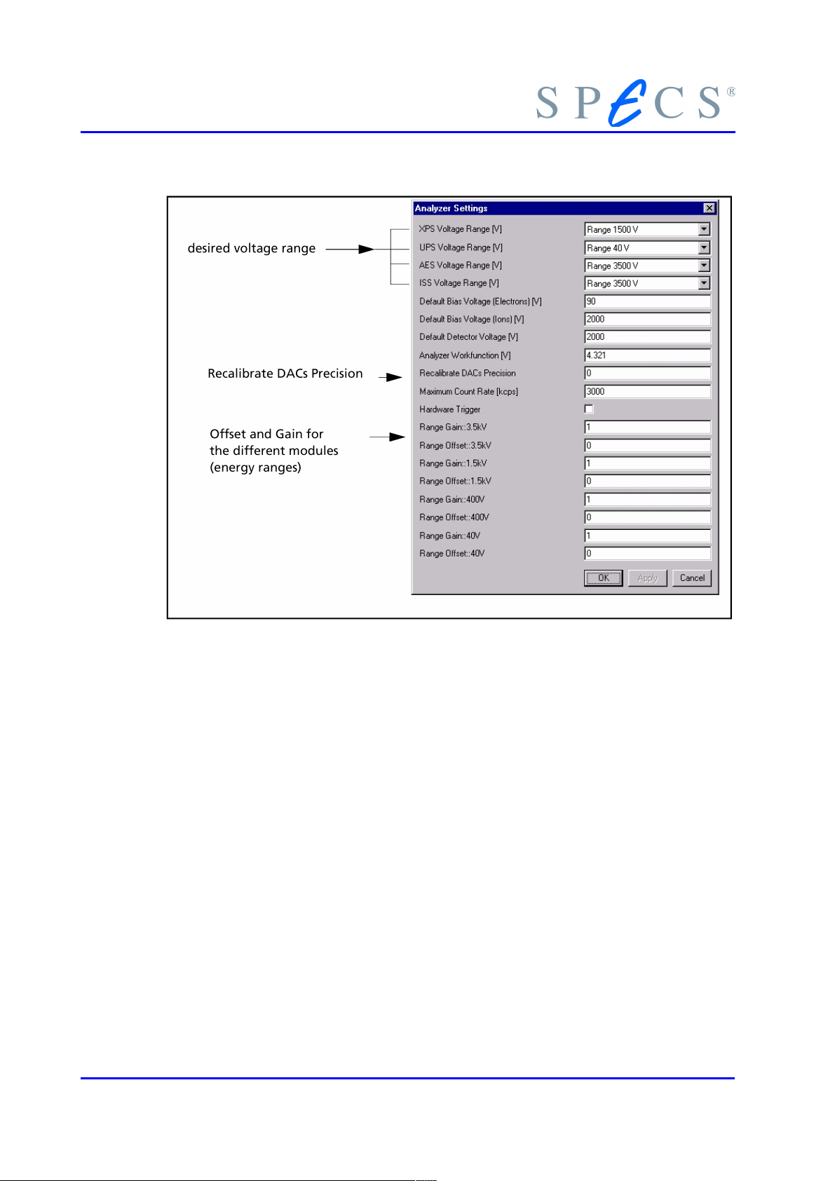
Calibration
Figure 26: Menu - “Analyzer Settings”
7.1 Complete Calibration Procedure
A complete calibration procedure consists of (see Figure 27: Analyzer Cailbration Procedure page 59):
1. Check/set offset and gain with voltmeter, i.e. the calibration of the modules via
high precision voltmeter and high voltage probe (section on page )
2. “MCD Calibration” , i.e. the estimation of the energy shifts of the single channels for selectable slit/lens combinations (see section 7.3 on page 60), which includes the calibration of the peak position independent of pass energy (see section 8.1 on page 65)
If the achieved values differ substantially from the existing default values or a
strong dependence on pass energy is observed for the spectra, this can point out
an analyzer malfunction which can not be corrected by the calibration procedure.
Please contact SPECS and send some spectra to assist in diagnosis.
3. the estimation of the analyzer workfunction (see section 7.4 on page 61) and
fine tuning of the offset for all modules (except 40V) via Fermi edge measurements (Figure 29: Fermi Edge Operation page 62) and optionally
58 PHOIBOS
Page 65
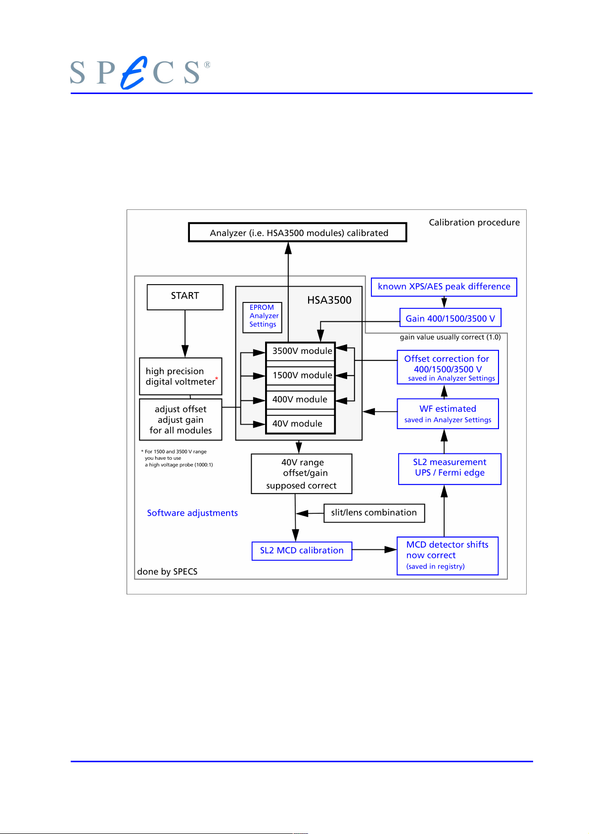
Complete Calibration Procedure
4. Gain calibration with XPS. A calibration check for the gain of the 1500V and
3500V modules see section 7.7 on page 64
5. and in section 8.2.2 , "Check Peak Position" on page 66, verify that the peak position in an XPS fit to the modifications of offset and gain performed in the selected range.
Figure 27: Analyzer Cailbration Procedure
7.2 Recalibrate the DAC Precision
Note: the power supply needs time to warm up. A self calibration procedure for the
DACs is run every time the power is switched on. You should restart the DAC calibration
procedure after a warm up (5-15min, switch off/on or use the field “Recalibrate DAC
Precision” in the menu ’Analyzer/Settings’ figure 26, page 58). Temperature stability as
PHOIBOS 59
Page 66
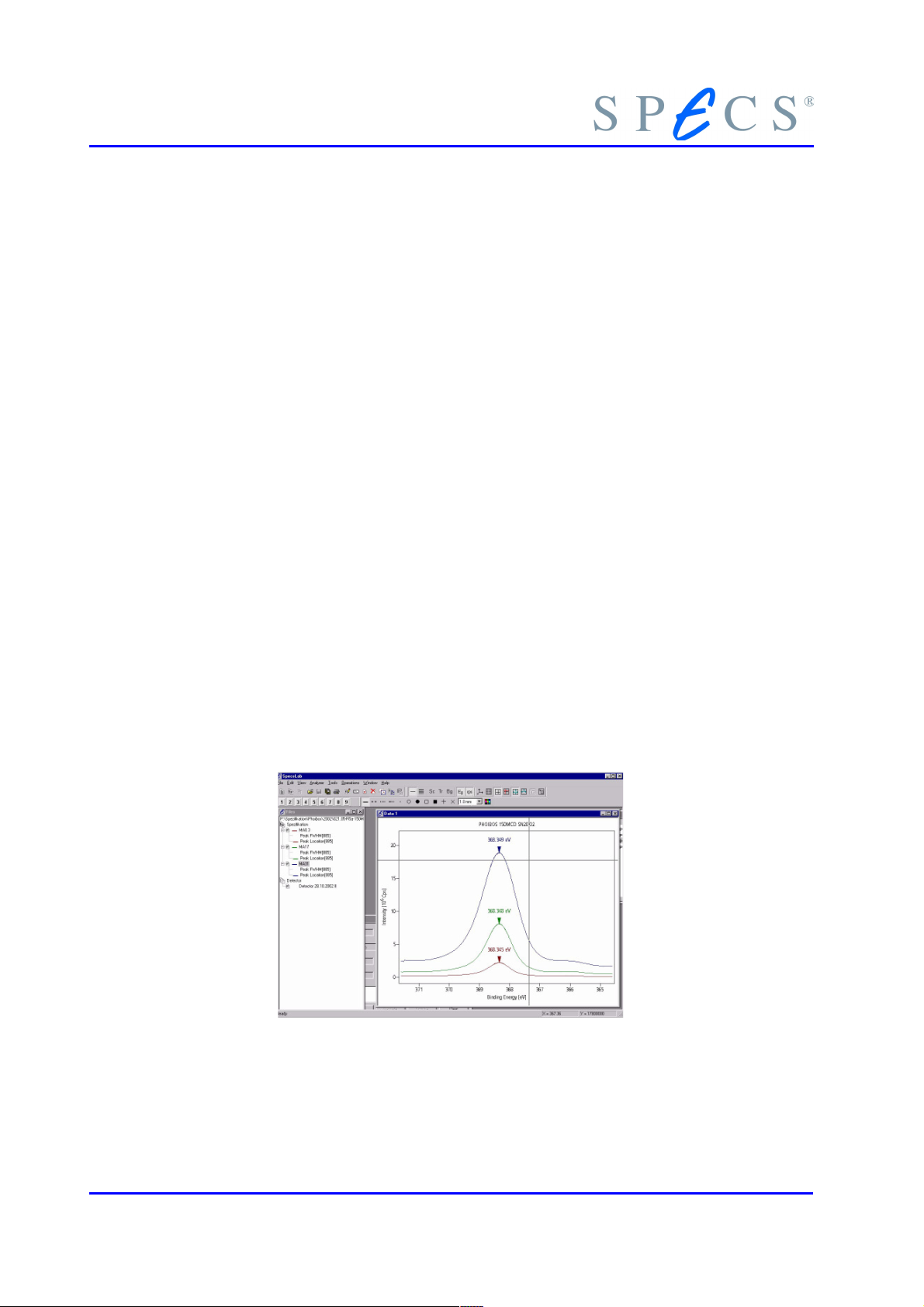
Calibration
well as sample charging or contamination of the surfaces inside the analyzer can influence your calibration.
Perform a manual “Recalibrate DAC” procedure to increase the accuracy to the possible
maximum if you have already warmed up the supply for at least 1 hour (e.g. type in a
value of 64).
7.3 MCD Calibration
SpecsLab2 software supports a calibration procedure named “MCD Calibration” in the
“Tools” menu. (The procedure should be used for the calibration of single channel detectors also.) Because of the energy shift between the single channels for a given kinetic energy (section 3.2 , "Hemispherical Analyzer (HSA)" on page 18) and the depend-
ence of the transmitted energy range of α (acceptance angle, see equation 5, page 18)
the detector shifts are different for each lens / slit combination. For the most common
lens / slit combinations, the values defined by SPECS and implemented in the software
give a good approximation. Nevertheless, the most commonly used lens / slit combinations should be calibrated by the customer again to prevent loss of performance.
You can easily check that the values are correct if you display the single channels and
compare the energy position of each channel. Second compare two different pass energies. Large differences suggest the need to calibrate this lens / slit combination as described below:
1. Identify a single high intensity peak in your data and set up a region that only
measures this peak.
2. Open a separate group with identical regions except pass energy for a single
peak within the region (e.g. pass energies 10, 20, 30eV).
Figure 28: MCD Calibration
3. Measure the regions.
4. Select the tool MCD Calibration in the “Tool” menu.
5. Calculate the ’Ek shift /Ep’ by pressing “Calculate” button.
60 PHOIBOS
Page 67
MCD Calibration
6. Check to see if the differences and the peak
position are reasonable. If the calculation
failed; check that the peak position can be
calculated for all regions. Mostly, regions
with low count rates (low pass energies) fail.
Move this region into another group and try
again (Drag and drop of the region via
mouse in the Files window). If you want to
check which region is causing the problems,
test that each single channel for the region
are able to perform the calculation (switch off noisy/wrong channels of the region and check if the peak location with “Tools”: “Peak Location” work, if work
also MCD calibration will work).
7. Pressing the apply button will apply the calculated shifts to all chosen slit combination. The default values (registry entries) will be overwritten.
7.4 Work Function Calibration with UPS
UV excitation recommended. Please note the comments given in the section 3.6 “Work
Function” on page 34. Thermal, aging, or other effects can change the coating of the
analyzer and therefore the workfunction over time. Grounding the sample and the
power supply influence the work function as well. The default workfunction value can
be corrected in the software in the Menu ’Analyzer/Settings’, see Figure 26. If you are in
doubt about the accuracy of the power supply it is recommended to perform the test /
calibration described in section "" on page first. Note the voltage range used while
measuring;: 40V, 400V, 1500V or 3500V (see SpecsLab2 menu ’Analyzer/Settings’).
1. Warm up the HSA3500 at least 10min. Switch off and on again to reboot and
force a startup calibration or manually perform the recalibration of the DACs
(section 7.2 on page 59).
2. Set the voltage range for the UPS measurement mode in the Menu
’Analyzer/Settings’, see Figure 26, to 40V.
3. Switch to the binding energy scale. Measure the position of the fermi edge (e.g.
+0.2 to -0.2 eV binding energy, and select HeI (if He I of course is used) in the
dummy source of the Menu ’Analyzer/Settings’ Sources selected). (The tool Op-
eration/Fermi Edge in the SpecsLab2 program as well as the cursor and differ-
ence cursor cross (black/red cross icon, left/right mouse button) simplifies the
procedure.)
4. Calculate the energy difference between expected and measured fermi edge.
5. Note that the high precision measurement with the digital voltmeter for offset
and gain are considered as correct and therefore, especially for the 40 V module, no further change for offset and gain is recommended. Once the measured
values for this range are correct, than it is possibile to estimate the work function.
Correct the default work function value in the Menu ’Analyzer/Settings’.
If the measured difference should be larger than 50meV perform the measurement as described in section , "" on page and change the values. Note that
PHOIBOS 61
Page 68
Calibration
voltmeter precision and poor grounding of the sample can falsify the calibration!
The work function correction will be applied to all modules!
6. Check the result with new spectra.
Figure 29: Fermi Edge Operation
Note the advice given in section 7.2 , "Recalibrate the DAC Precision" on page 59
For more detailed information please contact SPECS support.
7.5 Work Function Calibration with XPS
Please note the comments given in section 3.6, “Work Function” on page 34 and in the
description in section 7.4.
Instead of the UV excitation (section 7.4), X-ray excitation is used to calibrate the Work
Function. Note that you have to select at least the 1500V range ( see SpecsLab2 menu
’Analyzer/Settings’) in case of Mg/Al Kalpha excitation. This voltage ranges has a lower
accuracy than the 40V range ( on page ).
7.6 Offset Calibration with UPS
UV excitation recommended. Please note the comments given in the paragraph “Work
Function” on page 35 and the comments given in section 7.4.
Thermal or other effects can change the accuracy of the offset and gain over time. This
can be compensated for with the software. The values for the energy ranges can be
changed separately in the Menu ’Analyzer/Settings’, see Figure 26. The procedure described in “Work Function Calibration with UPS” on page 58 as well as section , "" on
page should be done first if there are any doubts about the supply’s accuracy or the
Work Function setting.
62 PHOIBOS
Page 69
Offset Calibration with UPS
Note the voltage range used while measuring. For adjustment, the desired range
should be selected according to the used method : i.e. 40V, 400V, 1500V or 3500V in the
active method row of Analyzer settings (see SpecsLab2 menu ’Analyzer/Settings’).
1. Warm up the HSA3500 at least 10min. Switch off and on again to reboot and
force a startup calibration or manually perform the recalibration of the DACs
(section 7.2 on page 59).
2. Set the voltage range for the UPS measurement mode in the Menu
’Analyzer/Settings’, see Figure 26, to 40V.
3. Switch to the binding energy scale. Measure the position of the fermi edge (e.g.
+0.2 to -0.2 eV binding energy, and select HeI (if He I of course is used) in the
dummy source of the Menu ’Analyzer/Settings’ Sources selected). (The tool Operation/Fermi Edge in the SpecsLab2 program as well as the cursor and difference cursor cross (black/red cross icon, left/right mouse button) simplifies the
procedure.)
4. Note the comments given in section 7.4 , "Work Function Calibration with UPS"
on page 61.
5. Use this 40V range result as the reference point for the other voltage ranges.
6. Select one of the other voltage ranges (400/1500/3500V) in Menu ’Analyzer/Settings’ and perform a Fermi edge measurement like for the 40 V range.
7. Compare the result with the 40V range spectra.
8. Calculate the energy difference between expected and measured Fermi edge
(the usual difference is less than 0.2 eV, more suggest a hardware error). Set the
offset for the selected voltage range (use binding energy values to get the correct polarity for the offset).
9. Set the offset of the used energy module to the calculated value in the menu
analyzer settings.
10. Measure again and repeat the procedure for each of the other desired voltage
ranges.
Note the advice given in section 7.2 , "Recalibrate the DAC Precision" on page 59.
Figure 30: Fermi Edge Operation
PHOIBOS 63
Page 70

Calibration
gain
=
distance
848.66
eV
For more detailed information please contact SPECS support.
7.7 Gain Calibration with XPS
See section 8.2.1 , "Check Kinetic Energy Scale" on page 66. Run spectra for the gold
and the copper peak (use clean samples, sputtered). Measure the distance between the
peak maxima of gold and copper. If the value found differs strongly from 848.66 eV
please inform SPECS. You can correct the gain (default value = 1) by
(27)
Note the default voltage range you have used while measuring with the desired method (see SpecsLab2 menu ’Analyzer/Settings’).
64 PHOIBOS
Page 71

Chapter
8 Analyzer Checks
8.1 Independence of Peak Position with Pass Energy
Because of the large number of slit and lens combinations, the energy calibration of the
analyzer was not done for each slit combination. SPECS delivers the analyzer with the
correct parameters for the common slit combinations. To check the independence of
the peak position with pass energy for a desired slit combination please follow the procedure below:
Transfer a silver sample into the system. Warm up your electronics first!
Adjustments:
Excitation Mg Kα
X-ray power 100 W
Slit desired slit combination, e.g. entrance: largest slit / exit: open
Mode Medium Area
Binding energy range 365 - 375 eV
Scan 1
Dwell Time 100 msec
Energy step 25 - 30 meV
Pass energy ~ 15eV
Run a spectrum. Set a second pass energy (for the above described slit combination e.g.
of about ~5 eV). Repeat the measurement. Compare the spectra. If the voltages are correct, the peak-maxima of both spectra have to have the same energy. The peak positions of both spectra should not differ by more than 100 meV. For a symmetrical peak
the peak position is independent of Epass. This is not true for Auger electron peaks since
the peaks are intrinsically asymmetrical.
You can also display the single channels for the accumulated spectra. The difference in
the peak maxima for each channel indicates the quality of the MCD Calibration (see section 7.3). If the peak energy weakly depends on pass energy, perform the “MCD Calibration” (see section 7.3, page 60). If the calibration does not fix the problem and/or
there is a strong dependence please refer to section “” on page . Short circuits or supply failure can cause such behavior. After voltage check please contact SPECS and send
some spectra as well as the measured voltages to help diagnosis of the exact problem.
Note that there is a weak dependence of the peak energy on beam position at the
sample and the size of the illuminated area. Because SPECS calibrates the analyzer with
PHOIBOS 65
Page 72
Analyzer Checks
a broad illuminating X-ray source, additional “MCD Calibration” for the point source
may be required.
8.2 Energy Scale Tests with XPS
8.2.1 Check Kinetic Energy Scale
Transfer a gold/copper sample into the system. Clean carefully by ion sputtering. With
this sample the main peaks are separated far enough for calibration purposes. The Au
4f7/2 and Cu 2p3/2 peaks energy difference is 848.66 ± 0.03 eV
Adjustments:
Excitation Mg Kα
X-ray power 100 W
Slit entrance: largest slit / exit: open
Mode Medium Area
Binding energy range 82 - 86 eV for the Au 4f7/2 peak
Dwell Time 100 msec
Scan 1
Energy step 25 - 30 meV
Pass energy ~8 eV
930 - 937 eV for the Cu 2p3/2 peak
2
.
8.2.2 Check Peak Position
Check for proper peak positions corresponding to table 14 on page 67. If the peaks offset consistently, check if the proper peak position can be achieved by correcting the
Work Function, sections 7.4 - “Work Function Calibration with UPS” on page 61, 7.5 “Work Function Calibration with XPS” on page 62 or 7.7 - “Gain Calibration with XPS”
on page 64. If this is not the reason, a complete calibration (as described at the beginning of this chapter) is required or there is a failure in the analyzer or supply (chapter 6,
"Troubleshooting" on page 51).
Note: Strong displacement usually caused by poor contact inside the analyzer (see
“Connection check for the analyzer electrodes” on page 70) or control unit failure (see
“Control Unit Check” on page 61) .
Peak
Au 4f7/2 84.00 ± 0.01 83.98 ± 0.02
Ag 3d5/2 368.27 ± 0.01 368.26 ± 0.02
Cu 2p3/2 932.66 ± 0.02 932.67 ± 0.02
2 XPS: Binding Energy Calibration of Electron Spectrometers 5 - Re-evaluation of the Reference Energies.
M.P.Seah, I.S.Gilman and G. Beamson, Surfaceand Interface Analysis 26, 642-649 (1998)
Mg Kα
Binding Energy, eV
Binding Energy, eV
Al Kα
66 PHOIBOS
Page 73

Energy Scale Tests with XPS
Cu L3MM 334.94 ± 0.01 567.96 ± 0.02
Table 14: Calibration Binding Energies for non-monochromated Mg Kα X-rays
8.3 Specification Check
8.3.1 Survey Spectrum of Silver
The XPS performance of an energy analyzer is usually determined using a silver sample.
A clean silver sample is introduced into the vacuum chamber and cleaned by ion sputtering. Use the same settings as in the overview spectrum of silver enclosed with the
Specification Report on the analyzer. For example:
Excitation Mg Kα
X-ray power 300 W
Slit entrance: largest slit / exit: open
Mode Medium Area
Binding energy range 1000 - 0 eV
Energy step ~300 meV
Dwell Time 100 ms
Pass energy ~13 eV
A typical XPS overview spectrum taken with a PHOIBOS analyzer on silver is shown below (figure 31).
PHOIBOS 67
Page 74
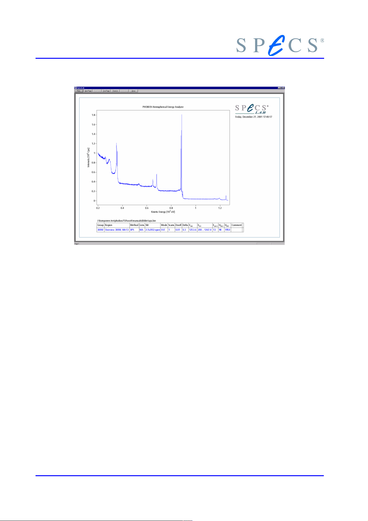
Analyzer Checks
Figure 31: XPS on Silver, Wide Scan (PHOIBOS 150 MCD9)
Parameters for the survey spectrum in figure 33:
Lens mode: Medium Area
Slit: entrance: largest slit / exit: open
Sample current: 160 nA at 300W Mg Kα
8.3.2 Intensity and Resolution
Use the same settings as in the Ag spectra enclosed with the Specification Report on the
analyzer.
For example:
Excitation Mg Kα
X-ray power 300 W
Slit entrance: largest slit / exit: open
Mode Medium Area
Bin. energy range 378 - 364 eV
Dwell Time 100 msec
No. of scans 1
Step width 25 - 30 meV
Pass energy 8-9 eV
A well resolved Ag 3d doublet is shown in figure 32. This spectrum is typical for a
PHOIBOS.
68 PHOIBOS
Page 75

Specification Check
The signal (net intensity, i.e. peak count above background) of the Ag 3d5/2 peak is
about 85-200 kcps/channel depending on the sample to X-ray source distance. The background in this case is defined as a straight line between the two neighbouring valleys
on both sides of the peak. The FWHM of the Ag 3d5/2 peak is calculated by measuring
the peak width at the half height between the peak maximum and the background.
Note:
Because of considerable spread in the gain of different CEM‘s, the voltage required for
the signal may differ from the specifications (see section 9.2). Pay attention to the detector voltage value in the Specification Report for the analyzer. Monitor the aging of
the channeltrons monthly and adjust the default detector voltage.
If the measured spectra and values differ substantially from those in the Specification
Report of the analyzer, it may be necessary to sputter the sample again or optimize the
sample and X-ray source positions, or a HSA 3500 calibration might be needed. Oxidation of the anode material may also lead to peak broadening.
In many cases it is helpful to know the intensities, signals, and accompanying FWHMs at
different pass energies. The measurements described above should be made at pass energies e.g. of 2, 5, 10, 20 and 50eV for largest slit and up to 200 eV for the 1mm slit diameter. The Dwell Time or number of scans should be adapted to the pass energies in
such a way that the maximum intensities (in counts not in counts per second) are about
the same in every case. Namely, for low pass energies, choose a higher Dwell Time than
for high pass energies. This gives comparable counting statistics for all measurements.
PHOIBOS 69
Page 76
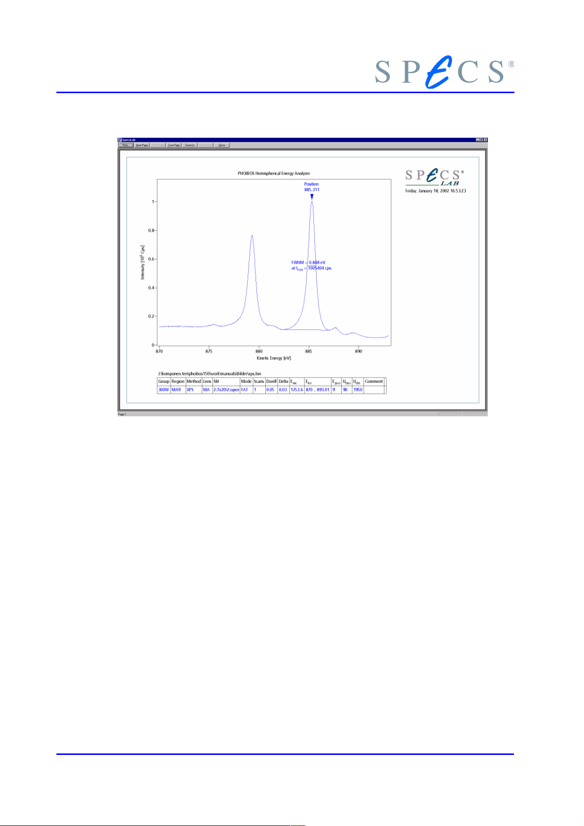
Analyzer Checks
Figure 32: XPS on Silver, Ag 3d (PHOIBOS 150 MCD9)
Parameter for the Ag 3d spectrum in figure 34:
Lens mode: Medium Area
Slit: 2:7 x 20 mm / 2:open
Sample current: 160 nA 300W Mg Kα
Detector voltage: 1950 V
If no spectrum but a straight line appears after the control unit has been started, either
no pulses are arriving at the control unit counter, the counter is defective, or the spectrometer voltage U0 is missing. The following checks should be made:
1. All cable connections (Figure 2: Connection Scheme page 7) between has 3500
and Detection box PCU 300 the computer and the EC10 Ethernet-Can-Adapter.
2. Control Unit Check, see section
3. Preamplifier, see section 9.1
4. Section 9.2, “Detector Voltage” on page 76.
8.4 Connection Check of the Analyzer Electrodes
In addition to this test, the correct generation of the spectrometer voltages should be
checked (see section , "" on page ).
70 PHOIBOS
Page 77
Connection Check of the Analyzer Electrodes
8.4.1 Capacitance Check for Electrodes
Check the electrode connection to the electrical feedthrough. For this check a capacitance meter must be used. The best way to check is to measure the capacitances
between the housing and all pins of the feedthrough of the analyzer (see Figure 33:
Schematics of the 12-pin Analyzer Feedthrough, page 72.). Switch off the HSA 3500 and
remove the connector to the HSA electrodes.
! Mind the safety information given at the beginning of this manual!
The capacitances measured on the HSA and lens electrodes under UHV conditions in
table 16, and table 17 are for information only. Some differences caused by the meter
should be taken into consideration when checking the values. Correct ratios between
the values show correct connection to the analyzer parts, the absolute values may differ
from the values in the table. Tables of former releases can be found in the documents
“Check-PHOIBOSRx.pdf”.
PIN 1 2 3 4 5 6 7 8 9 10 11 12
housing 32 147 123 37 121 - 65 71 323 62 170
Table 15: Capacitance Measurements (pF), PHOIBOS100 R6 or higher
PIN 1 2 3 4 5 6 7 8 9 10 11 12
housing 60 191 139 63 124 - 71 79 396 109 303
Table 16: Capacitance Measurements (pF), PHOIBOS150 R6 or higher
If the measured capacitances differ substantially from the nominal values please contact
SPECS. If the capacitances have nearly the right values, no short circuit inside the spectrometer is likely. If the measured capacitances have the correct values, a missing contact from the HSA 3500 to the analyzer may be the reason for a faulty spectrum (see
section 8.4.2 , " on page 71).
8.4.2 Check the Cable Contacts
The connection to the analyzer and the detector are supplied by two multi-pin vacuum
feedthroughs, which are designed for high voltages up to 5 kV. Check whether the contacts are in good condition. Since the plug is a movable part which is frequently
plugged and unplugged, it can become defective. In most cases, contact failures in the
plug are the reason.
● A 12-pin feedthrough on a flange DN38CF, mounted to the lens housing, for all
voltages of lens electrodes and capacitor electrodes, which is schematically
shown in figure 33, page 72.
● The second 12-pin feedthrough (DN38CF) mounted at the detector flange, for
all channeltron voltages and channeltron outputs. The pin assignments is shown
in figure 33, page 72.
PHOIBOS 71
Page 78
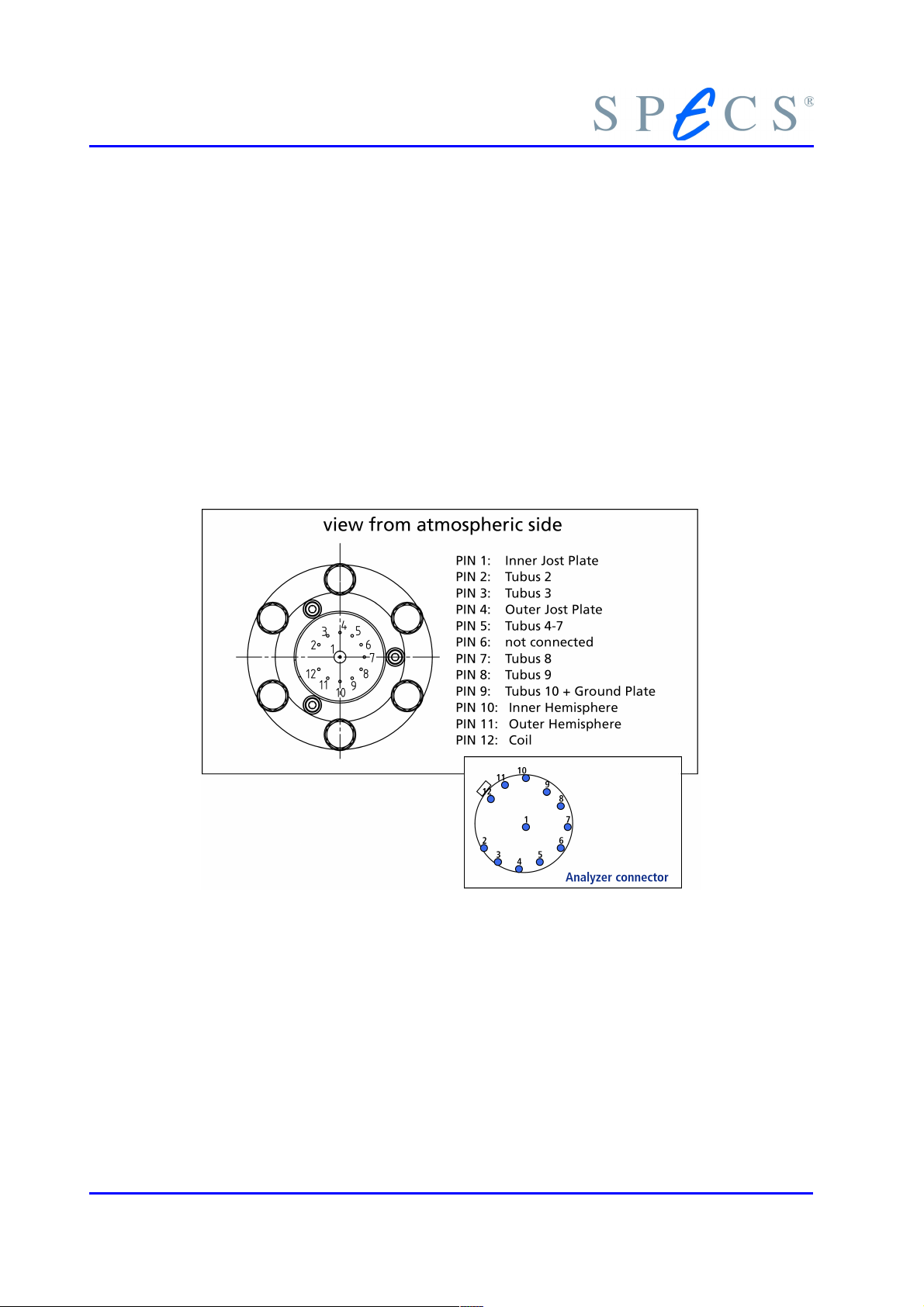
Analyzer Checks
Figure 33: Schematics of the 12-pin Analyzer Feedthrough
72 PHOIBOS
Page 79
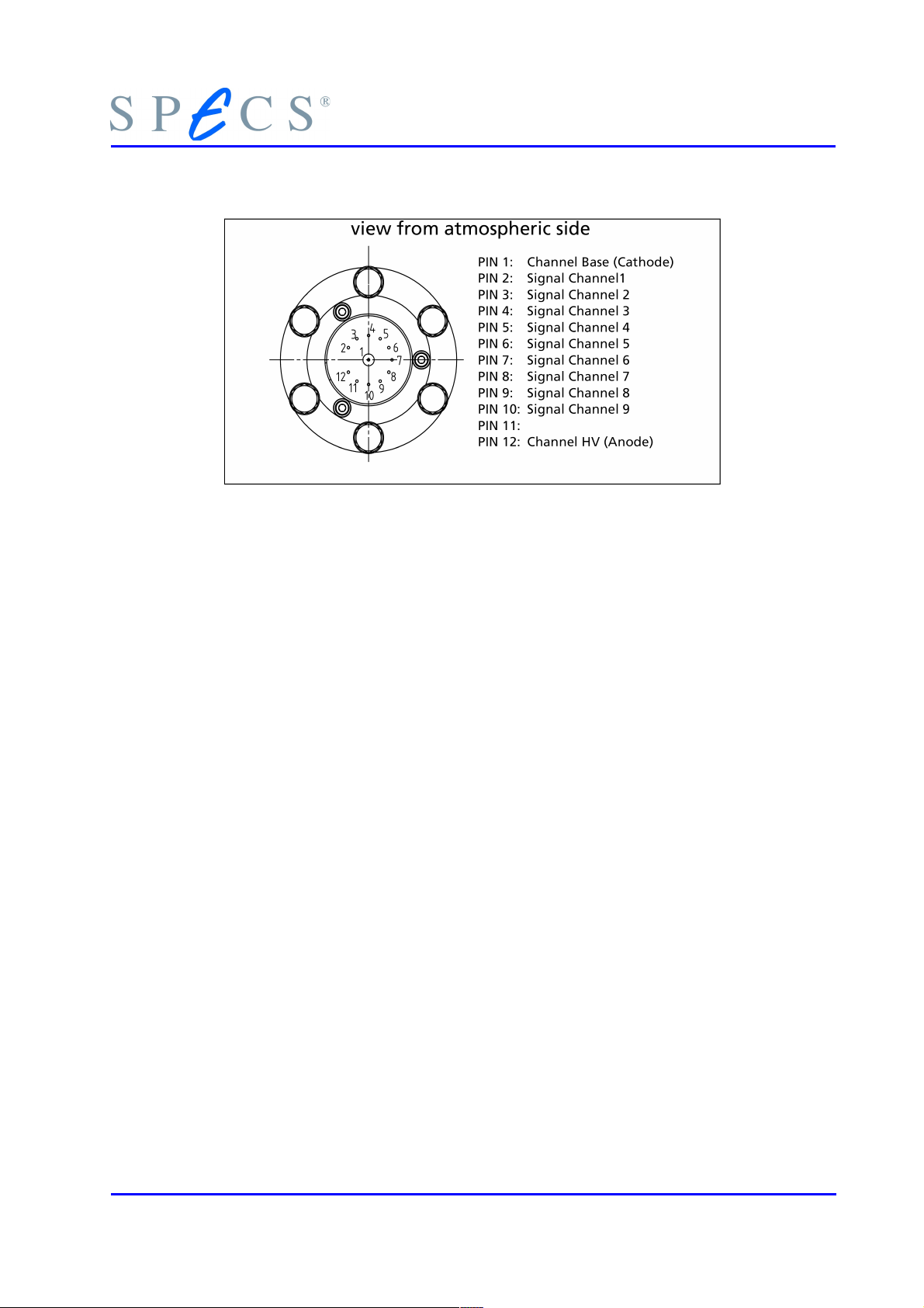
Connection Check of the Analyzer Electrodes
Figure 34: Schematics of the 12 pin Detector Feedthrough
8.5 Check all analyzer voltages
This section has been moved to the HSA3500 Manual.
PHOIBOS 73
Page 80

Page 81

Noise
~3×=3×
signal[counts
]
Chapter
9 Deflector Settings
9.1 Preamplifier
9.1.1 Discriminator
Check the discriminator threshold using the noise of the signal within one spectrum.
The square root of the signal (counts! not counts/second) should be equal to the RMS
(root mean square) of the noise at this energy (i.e. the value mean signal +/- 3 x RMS
should include nearly all data points). The noise value without excitation source should
be only few counts per second and channel.
Threshold Value:
Use the fixed mode of the acquisition software (see SpecsLab2 manual) to estimate the
noise at constant kinetic energy for the acquired signal and compare with the square
root of the signal (counts not cps!).
(28)
Normally the discriminator threshold does not have to be changed. If necessary, the
threshold can be adjusted in the menu ’Analyzer/Settings’. Increasing the threshold
level causes a shift of the detector starting point and plateau towards higher voltages,
but helps to suppress possible channeltron differences (noise, etc.). Usual threshold values are in the range between 2 and 10mV.
PHOIBOS 75
Page 82
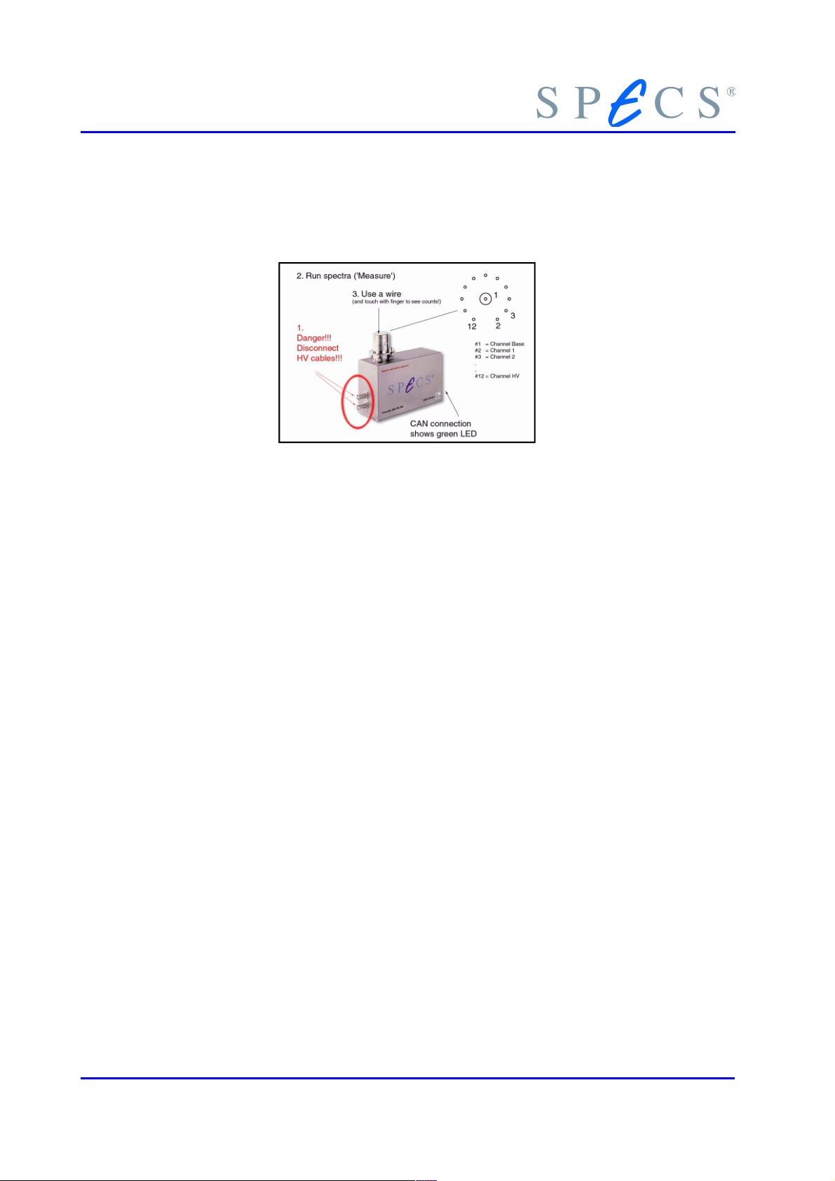
Deflector Settings
9.1.2 Amplifier Check
Figure 35: PCU Amplifier Test
Caution
Set the detector voltage to zero and disconnect
both HV cables CHANNEL HV and CHANNEL BASE!
! Mind the safety information given at the beginning of this manual!
Disconnect the detector box (preamplifier is inside) from the detector flange. Run a
spectrum. Touching each pin of the preamplifier connector with a piece of wire results
in a signal. A signal must be observed for each channel. If no signal is observed for
some channels, these channels of the MCD preamplifier are not ok. If no signal is observed for all channels or a constant signal is observed, check the preamplifier power
(green LED).
Note: If the maximum count rate is achieved the measurement will stop. To avoid this,
increase the discriminator level to about 15mV or use a resistor of about 100 Ohm for
the check. The default detector threshold is between 2 and 10mV. Do not forget to set
the discriminator back to the original or desired values.
9.2 Detector Voltage
Because of a considerable spread in the gain of different multipliers and the threshold
level used, the voltage required for the signal for the installed detection system may
differ. Pay attention to the detector voltage value in the Specification Report sent with
the analyzer. Basically, a working detector voltage is the detector voltage at the beginning of the detector plateau (DetectorVoltageScan, see Figure 15: Detector Sweep,
Count rate vs. Voltage, page 30) and has to be checked monthly.
76 PHOIBOS
Page 83

Noise
9.3 Noise
Depending on the environment of the analyzer (ground, feedthrough connection
status, ... ), the handling during transport / installation (bake out, dust, ...) and the history of of operation (vacuum, gas load, total amount of accumulated charged particles,
etc.) some or all channels may show noise without any excitation. If the “Amplifier
Check” on page 80 shows that the amplifier is working correctly, the grounding of the
analyzer is ok; by following the advice given in sections 3.5 - “Single and Multichannel
Detector (SCD) / (MCD)” on page 25 and in section 9.1.1 - “Discriminator” on page 75 ,
the noisy channels can be suppressed. First, try to set the threshold of the noisy channel
to higher value (up to 10 mV). This will also shift the working point for the channeltron
(see “The Working Point of the CEM’s” on page 27). If this does not help, completely
suppress the channel. To continue to work with the analyzer (up to the replace of the
defective part) without the signal from the noisy channels:
● Suppress a noisy channel (section 9.3.1 )
● Switch off certain channels (section 9.3.2 )
9.3.1 Suppress a Noisy Channel
In some cases a channeltron becomes noisy (dust, contamination, overheated, etc.). To
avoid disturbing the acquisition of the other channeltrons, increase the threshold level
for this channel (Figure 26: Menu - “Analyzer Settings”, page 54). Note: You have to select the desired channel first before changing the value to 120mV (maximum) for example.
To reset all channels to the same value select ’all’.
9.3.2 Switch off Certain Channels
To switch off certain channels, it is necessary to modify the registry entry for the
HSA3500Analyzer key. For a 150R5c type of analyzer the entry "CounterChannelMask"
is located at
"HKEY_LOCAL_MACHINE\SOFTWARE\Specs\Hsa3500Analyzer\Phoibos-Hsa3500\150 R5c"
The necessary type is “binary”. Create such a binary entry if it does not exist (Figure 36:
CounterChannelMask for MCD9, 1+2+8+9 off, page 78). Please also refer to the description about the registry entries in the SpecsLab2 manual.
The software masks not only the channels, but the detector shifts and channel gains
too. In the selection for the channels in the SpecsLab2 analyzer/settings menu the consecutive numbering of the remaining channels start with 1 and end with the number of
the available channels.
Note: After any hardware change (i.e. channel replacement), or any registry change (as
above), it is recommended to perform an MCD Calibration routine.
PHOIBOS 77
Page 84
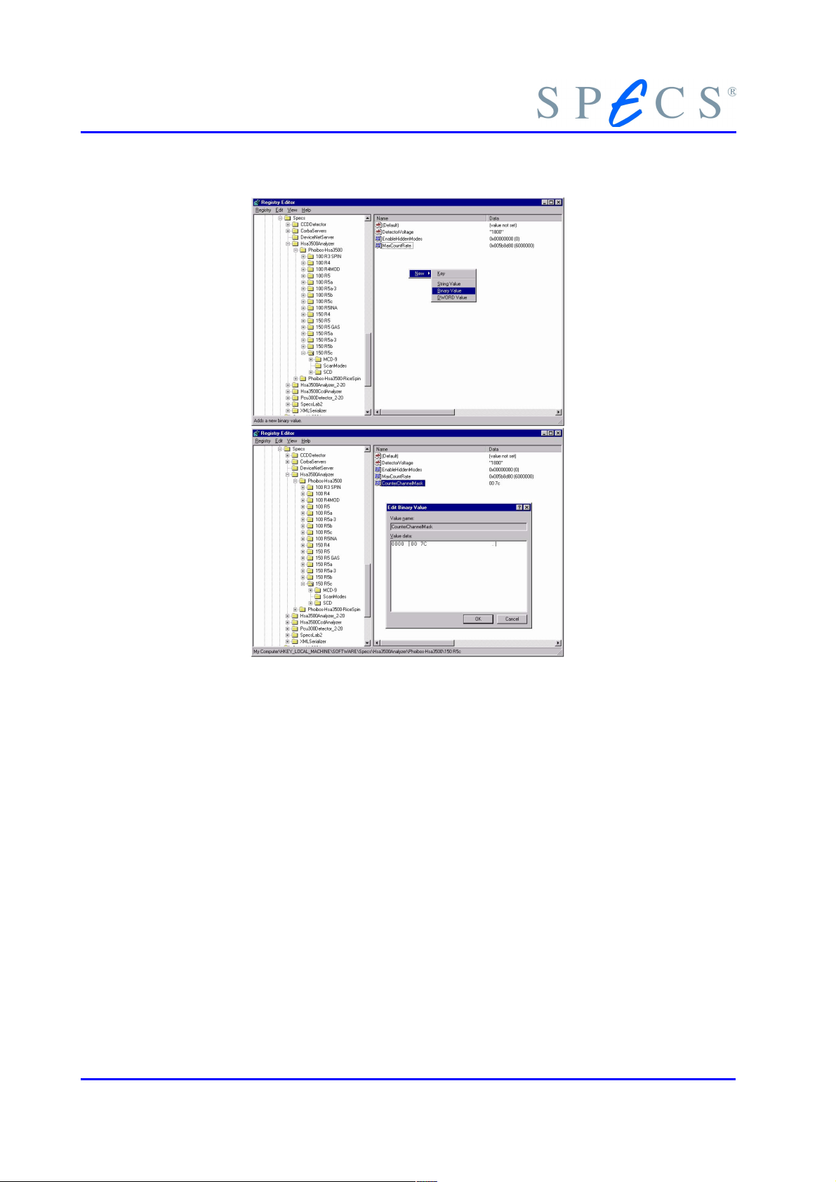
Deflector Settings
Figure 36: CounterChannelMask for MCD9, 1+2+8+9 off
9.3.2.1 Mask example for MCD9
The *.reg CounterChannelMask entry for a MCD9 type ’PHOIBOS 150 R5c’ looks like:
Each bit represents one channel. A 9 channel MCD for example has following mask
’00000001 11111111’ or as hexadecimal ’01 FF’. Please note that the first bit from the
left is channel number 1 and the last to the right is channel 9 or 5 respectively. Therfore
all channels means
[HKEY_LOCAL_MACHINE\SOFTWARE\Specs\Hsa3500Analyzer\Phoibos-Hsa3500\150 R5c]"
CounterChannelMask"=’01 ff’
To achieve that a 9 channel detector only use 5 channels you have to change to
00000000 01111100 or ’00 7C’. The *.reg file for a MCD9 with channel 1,2 and 8,9
switched off looks like following:
[HKEY_LOCAL_MACHINE\SOFTWARE\Specs\Hsa3500Analyzer\Phoibos-Hsa3500\150 R5c]
"CounterChannelMask"=’00 7C’
78 PHOIBOS
Page 85

Noise
9.3.2.2 Mask example for MCD5
The *.reg CounterChannelMask entry for a MCD5 type ’PHOIBOS 100 MCD R5c’ looks
like:
A 5 channel MCD has following mask ’00000000 00011111’ or as hexadecimal ’00 1F’.
Please note that the first ’1’ from the left is channel number 1 and the last digit on the
right side is channel 5 respectively.
Therfore all channel means
[HKEY_LOCAL_MACHINE\SOFTWARE\Specs\Hsa3500Analyzer\Phoibos-Hsa3500\100 R5c]
"CounterChannelMask"=’01 1F’
To achieve that a 5 channel detector only use channels #1,2 and 4 you have to change
to 0000000 00011010 or ’ 01 10’, i.e.
[HKEY_LOCAL_MACHINE\SOFTWARE\Specs\Hsa3500Analyzer\Phoibos-Hsa3500\100 R5c]
"CounterChannelMask"=’01 10’
PHOIBOS 79
Page 86

Page 87

Chapter
10 Spare Parts
10.1 Cu Gasket
All CF gaskets are custom made by SPECS. In case you need a replacement please contact SPECS, because it depends on the release of the analyzer.
The serial number of the analyzer is marked on the lens flange.
10.2 Multiplier
1. SCD, Single Channel Electron Multiplier replacement for PHOIBOS analyzer
2. MCD, CEM Array replacement
5 channels MCD for PHOIBOS analyzer
9 channels MCD for PHOIBOS analyzer
Please indicate the serial number of your analyzer (flange at the lens housing, e.g.
33.04) in the replacement order. The order of a single channeltrons, a set of channeltrons or a complete replacement of the detector flange including channeltrons is possible.
10.2.1 Channeltron Handling and Storage
A channeltron or a channeltron array (array of 5 or 9 of single channel multipliers,
fused together in a precision matrix) is a high gain device for detecting energetic
particles such as electron and ions, or radiation. The channeltron consists of a small,
curved glass tube. The inside wall is coated with a high resistance material. The resistive
material becomes a continuous dynode when a potential is applied between the ends
of the tube. It is fabricated from a lead-doped glass. Proper handling is required and
the following precautions must be taken.
10.2.1.1 Handling of the Multiplier
● Shipping containers should be opened only under clean, dust-free conditions.
● No physical object should come in contact with the active area of the detector.
The channeltron should be handled by its solid borders using clean, decreased
tools fabricated from stainless steel, teflon (PTFE) or other UHV compatible
materials.
PHOIBOS 81
Page 88

Spare Parts
● The channeltrons should be protected from exposure to particle contamination.
Particles which become affixed to the plate can be removed by using a singlehair brush and an ionized dry nitrogen gun.
10.2.1.2 Operation of the Multiplier
Microchannel plates and Channeltron detectors can be degraded by exposure to various
types of hydrocarbon materials which raise the work function of the surface, causing
gain degradation. Operation in a clean vacuum environment of 10
-5
mbar or better is
necessary in order to ensure the long-life characteristics of these devices.
10.2.1.3 Storage of the Multiplier
Due to the hygroscopic nature of the doped lead glass, it is important that the channeltrons are stored properly.
Warning:
The shipping containers are not suitable for storage periods exceeding the delivery
time. Upon delivery to the customer‘s facility, channeltrons must be transferred to a
suitable long term storage medium.
● The most effective long term storage condition for the channeltron is a clean
(oil free) vacuum.
● A dry box which utilizes an inert gas, such as argon or nitrogen heated above
the dew point, is also suitable.
● Desiccator cabinets that utilize silica gel or other solid desiccants to remove
moisture have been proven to be unacceptable.
10.2.2 Change a Channeltron
A multiplier loses its gain with operating time. It should be changed when a significant
degradation in amplification (i.e. intensity) is experienced or the detector voltage limit
of the control unit is reached.
10.2.2.1 Removing the Detector Flange
● Switch off the analyzer supply.
● Remove both the detector and analyzer connections.
● Vent the system.
● Open the detector flange, let the detector unit down slowly and put it carefully
on a table.
(Three springs, pressing the detector assembly to the groundplate may exert
some force downward when the screws are released.)
10.2.2.2 Replacing Channeltrons
● Note: Use dry nitrogen only in order to remove dust or lint.
● Loosen the three screws at the top plate and remove the plate.
82 PHOIBOS
Page 89
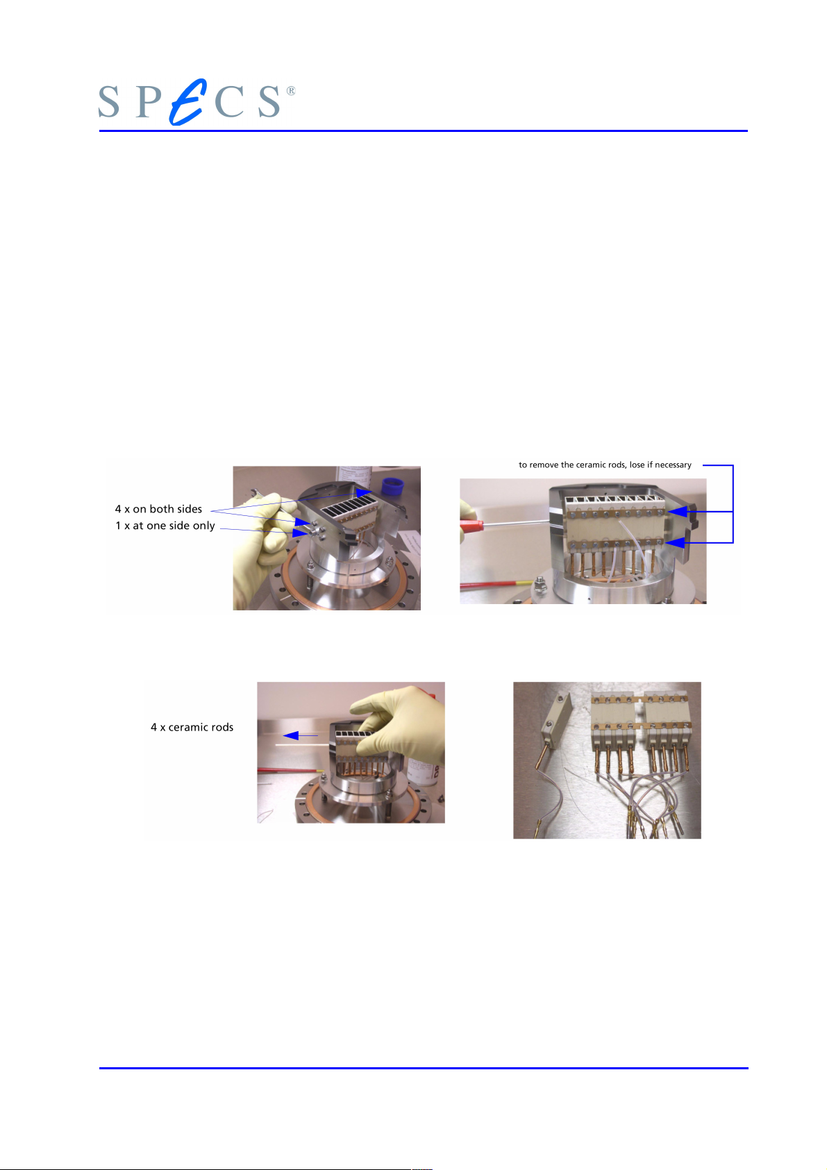
Multiplier
● Disconnect the cables.
● Note the orientation and alignment of the defective channeltrons.
● Release the screws which are fixing the ceramic rods. Release only one of the
adjustment screws. Do not change the other screws, this fixes the position for
the channeltrons with respect to the body when rebuilding the assembly(figure
37, page 83).
● Pull back the ceramic rods until the replacement of the channeltron is possible
(figure 38, page 83). If the ceramic rod is stuck, try to loosen the screws of each
channeltron a bit.
● Remove the channeltron.
● Put the new channeltron in place and rebuild in reverse order.
● Carefully fasten the connections with the screws. Note: A bad contact means
noisy channeltron!
● Check all channeltrons for proper mounting.
● Check all electrical connections (Figure 33: Schematics of the 12-pin Analyzer
Feedthrough, page 72).
Figure 37: Screws fixing the ceramic rods and adjustment crew
Figure 38: Pull back the Ceramic Rods, Remove the Channeltron
10.2.2.3 Mounting the Detector Flange
● Mount the detector flange in reverse order.
● Check that there is no short circuit for all the pins of the detector supply feed-
through to each other and to ground.
PHOIBOS 83
Page 90
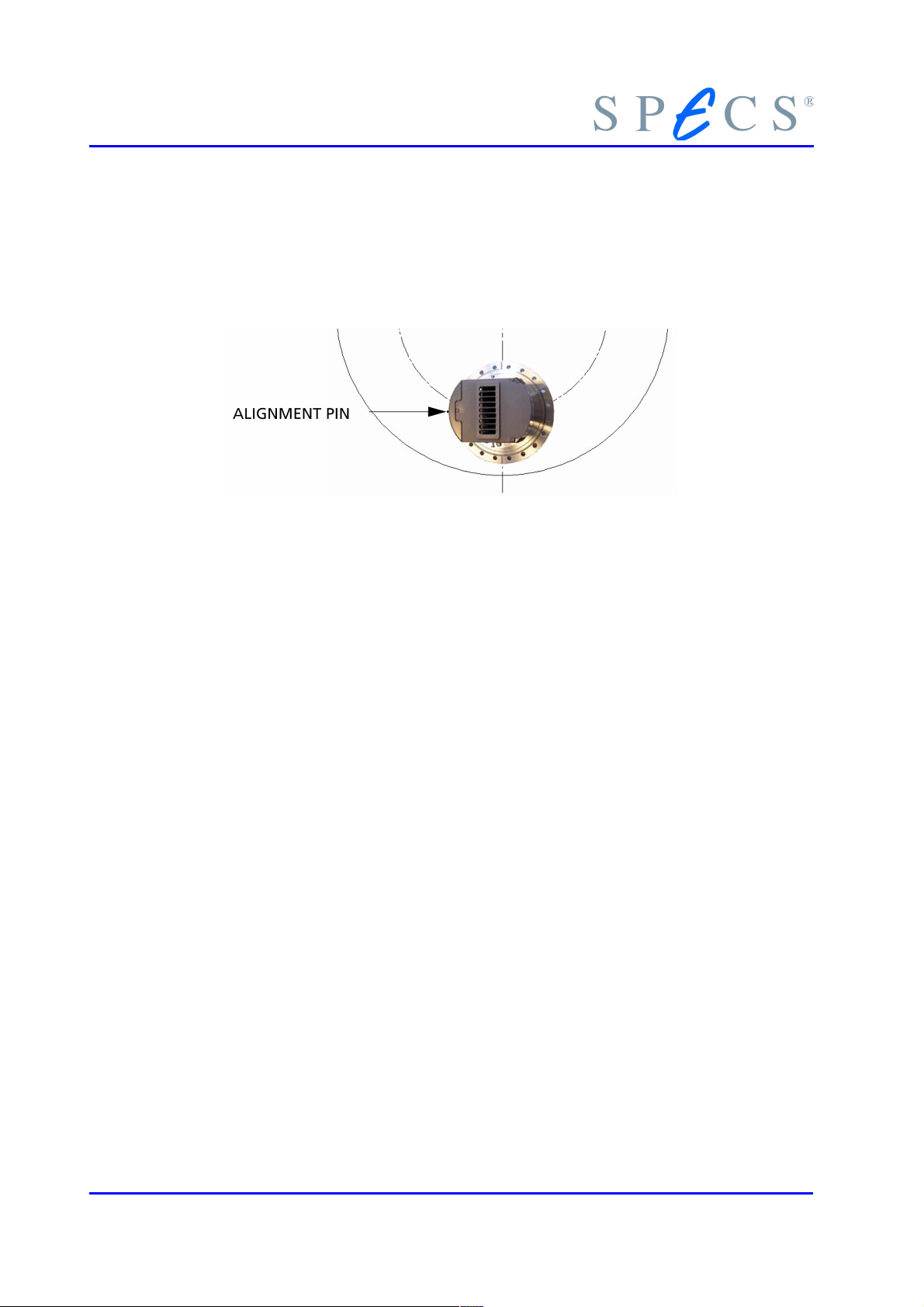
Spare Parts
● Looking into the opened detector flange from the bottom side you can locate a
'alignment hole' which corresponds to the part at the detector assembly (figure
39).
● Align the pin with the hole in the ground plate. Be sure that the detector is
nearly parallel to the ground plate and push the detector carefully into its seat.
Figure 39: Alignment Pin
● Pump down.
● Detector must be baked out at a vacuum pressure lower than 1⋅10
-6
mbar. It is
bakeable up to 200° C
● Check the detector according to section 8.3. (see Figure 15: Detector Sweep,
Count rate vs. Voltage page 29); checking the single channels in the acquisition
software may be enough.
84 PHOIBOS
Page 91

Chapter
LF List of Figures
Figure 1: Package Contents........................................................................................................................6
Figure 2: Connection Scheme....................................................................................................................7
Figure 3: Analyzer Housing (PHOIBOS100)...............................................................................................8
Figure 4: Analyzer Housing (PHOIBOS150)...............................................................................................9
Figure 5: Analyzer Main Components and Voltage Principle................................................................10
Figure 6: High Point Transmission Mode.................................................................................................13
Figure 7: Medium Area Mode..................................................................................................................14
Figure 8: High Magnification Mode........................................................................................................15
Figure 9: Typical Intensity-Position Profile with Iris Aperture................................................................17
Figure 10: PHOIBOS µ-Metal Shielding...................................................................................................21
Figure 11: Magnetic Field of the Trim Coil..............................................................................................22
Figure 12: External Rotary Dial for Positioning......................................................................................24
Figure 13: Entrance and Exit Slit Rings (Slit Combination 4-B)..............................................................24
Figure 14: Exit Slit Selection.....................................................................................................................25
Figure 15: Detector Sweep, Count rate vs. Voltage................................................................................29
Figure 16: Lifetime of the Extended Dynamic Range CEM....................................................................30
Figure 17: Linearity Plot for the new Extended Range CEM..................................................................31
Figure 18: Efficiency Plot for the new Extended Range CEM................................................................32
Figure 19: Detection Efficiency for Electrons and Ions...........................................................................33
Figure 20: Energy Scheme – Photoelectron Spectroscopy......................................................................34
Figure 21: Removal of the Transportation Locks....................................................................................38
Figure 22: Corresponding Hole in the Ground Plate..............................................................................39
Figure 23: Mounting Tips.........................................................................................................................42
Figure 24: Detector Flange.......................................................................................................................43
Figure 25: Starting up the detector.........................................................................................................48
Figure 26: Menu - “Analyzer Settings”...................................................................................................58
Figure 27: Analyzer Cailbration Procedure.............................................................................................59
Figure 28: MCD Calibration......................................................................................................................60
Figure 29: Fermi Edge Operation ...........................................................................................................62
Figure 30: Fermi Edge Operation ...........................................................................................................63
Figure 31: XPS on Silver, Wide Scan (PHOIBOS 150 MCD9)....................................................................68
Figure 32: XPS on Silver, Ag 3d (PHOIBOS 150 MCD9)...........................................................................70
Figure 33: Schematics of the 12-pin Analyzer Feedthrough..................................................................72
Figure 34: Schematics of the 12 pin Detector Feedthrough...................................................................73
Figure 35: PCU Amplifier Test..................................................................................................................76
Figure 36: CounterChannelMask for MCD9, 1+2+8+9 off......................................................................78
Figure 37: Screws fixing the ceramic rods and adjustment crew...........................................................83
Figure 38: Pull back the Ceramic Rods, Remove the Channeltron.........................................................83
PHOIBOS I
Page 92

List of Figures
Figure 39: Alignment Pin.........................................................................................................................84
II PHOIBOS
Page 93

List of Figures
PHOIBOS III
Page 94

Page 95

Chapter
LT List of Tables
Table 1: Acceptance Angle vs. Iris Diameter for a Point Source............................................................15
Table 2: Overview of the Lens Modes.....................................................................................................16
Table 3: Recommended Iris Values for Spatially Resolved Measurements............................................17
Table 4: Standard Slit Configuration.......................................................................................................23
Table 5: No Spectrum...............................................................................................................................52
Table 6: Low Intensity..............................................................................................................................53
Table 7: Low Energy Resolution..............................................................................................................53
Table 8: Peaks Shifted Equally.................................................................................................................54
Table 9: Peaks Shifted Differently...........................................................................................................54
Table 10: Intensity Fluctuations...............................................................................................................54
Table 11: High Background Signal..........................................................................................................54
Table 12: Noisy Spectrum.........................................................................................................................55
Table 13: Incorrect area was analyzed in all lens modes .......................................................................55
Table 14: Calibration Binding Energies for non-monochromated Mg Kα X-rays.................................67
Table 15: Capacitance Measurements (pF), PHOIBOS100 R6 or higher.................................................71
Table 16: Capacitance Measurements (pF), PHOIBOS150 R6 or higher.................................................71
PHOIBOS V
Page 96

Page 97

Chapter
I Index
A
Amplifier Check......3, 14, 16, 23,
27p., 30, 35, 37, 43p., 47pp., 55,
58pp., 65p., 70p., 77
Analyzer Alignment................40
Analyzer Checks......................65
Analyzer Feedthrough......22, 72
B
Baking Out..............................43
C
Cable Contacts.........................71
Calibration...............................57
Capacitance Measurements....71
CEM..........................................27
Change a Channeltron............82
Channeltron Handling............81
Check Peak Position................66
Coherence of Epass and Step. 26
Coil...........................................21
coil current..............................21
Connection Check...................70
Connection Scheme..................7
conversion voltage..................33
current module.......................22
D
DAC Precision..........................59
Detector Feedthrough............73
Detector Sweep.......................29
Detector Voltage.....................76
E
Electrical Connections...............6
Electron Multiplication...........27
Exit Slit.....................................24
Extended CEM.........................29
F
First Operation........................47
Functional Test........................49
H
Hemispherical Analyzer..........18
High Background....................54
Housing.....................................8
I
Intensity Fluctuations..............54
Introduction..............................1
ISS Operation...........................50
L
Lens System.............................12
lifetime.....................27p., 30, 49
Low Energy Resolution...........53
Low Intensity...........................53
M
Magnetic Coupling.................21
magnetic field.....20pp., 52p., 55
Magnetic Shielding.................20
MCD.........................................25
MCD Calibration......................60
Multichannel Detector............25
N
No Spectrum............................52
Noisy Channel..........................77
Noisy Spectrum........................55
P
Peaks Shifted...........................54
Q
Quick Start...............................47
R
Replacing Channeltrons..........82
S
Safety.................3, 5, , 44, 71, 76
sample distance.................40, 52
SCD...........................................25
Specification Check.................67
Spectrometer...........................11
Spectrometer Voltage.............33
Switch off certain channels.. . .77
System Description....................5
T
threshold.................................75
Trim Coil..................................21
U
Unpacking...............................37
V
Vacuum Installation................41
W
Work Function.........................34
working distance.........12, 40, 42
X
XPS (AES/UPS) Operation........49
XPS on Silver............................68
μ
-metal shieldingμ .............5, 20p.
PHOIBOS VII
Page 98

Index
PHOIBOS
Page 99

Health and Safety Declaration for used Vacuum
Equipment and Components
The repair and/or service of vacuum equipment/components can only be carried out if a correctly
completed declaration has been submitted for every component.
1.______________________________________________Description of components
Type: __________________________________________Serial No:_____________________
2. Reasons for return____________________________________________________________
3. Equipment condition
Has the equipment ever come into contact with the following (e.g. gases, liquids, evaporation
products, sputtering products ...)
Yes No
toxic substances?
•
corrosive substances?
•
microbiological substances (incl. sample material)?
•
radioactive substances (incl. sample material)?
•
• ionising particles/radiation (α, β, γ, neutrons, ...)?
Yes No
Is the equipment free from potentially harmful and hazardous
substances?
4. Decontamination Procedure
Please list all harmful substances, gases and by-products which have come into contact with the vacu-
um equipment/component during the decontamination methode used.
SUBSTANCE DECONTAMINATION METHODE
5. Legally Binding Declaration
Organisation:
Address:
Phone/Fax:
Name/Position:
I hereby declare that the information supplied on this form is complete and accurate.
Date:__________Signature:_____________Company stamp
Rev.: 0 1/1
 Loading...