

Page 1

SY-7VDA
Motherboard
****************************************************
VIA Cyrix III, Intel Pentium® III & Celeron
Processor supported
VIA PRO266 AGP/PCI Motherboard
66/100/133 MHz Front Side Bus supported
ATX Form Factor
****************************************************
User's Manual
Page 2

SOYO™ SY-7VDA
FC
Copyright © 2001 by Soyo Computer Inc.
Trademarks:
Soyo is the registered trademark of Soyo Computer Inc. All trademarks are the
properties of their owners.
Product Rights:
All names of the product and corporate mentioned in this publication are used for
identification purposes only. The registered trademarks and copyrights belong to
their respective companies.
Copyright Notice:
All rights reserved. This manual has been copyrighted by Soyo Computer Inc. No
part of this manual may be reproduced, transmitted, transcribed, translated into any
other language, or stored in a retrieval system, in any form or by any means, such
as by electronic, mechanical, magnetic, optical, chemical, manual or otherwise,
without permission in writing from Soyo Computer Inc.
Disclaimer:
Soyo Computer Inc. makes no representations or warranties regarding the contents
of this manual. We reserve the right to amend the manual or revise the
specifications of the product described in it from time to time without obligation to
notify any person of such revision or amend. The information contained in this
manual is provided to our customers for general use. Customers should be aware
that the personal computer field is subject to many patents. All of our customers
should ensure that their use of our products does not infringe upon any patents. It is
the policy of Soyo Computer Inc. to respect the valid patent rights of third parties
and not to infringe upon or to cause others to infringe upon such rights.
Restricted Rights Legend:
Use, duplication, or disclosure by the Government is subject to restrictions set
forth in subparagraph (c)(1)(ii) of the Rights in Technical Data and Computer
Software clause at 252.277-7013.
About This Guide:
This Quick Start Guide can help system manufacturers and end users in setting up
and installing the Motherboard. Information in this guide has been carefully
checked for reliability; however, to the correctness of the contents there is no
guarantee given. The information in this document is subject to amend without
notice.
For further information, please visit our Web Site on the Internet. The address is
"http://www.soyo.com.tw".
Edition: May 2001
Version 1.2
7VDA SERIAL
Tested To Comply
C
With FCC Standards
FOR HOME OR OFFICE USE
POST CONSUMER
100%
RECYCLED PAPER
ii
Page 3

Table of Contents SY-7VDA
Table of Contents
CHAPTER 1 MOTHERBOARD DESCRIPTION .............................1
1-1 INTRODUCTION...........................................................1
1-2 KEY FEATURES............................................................1
1-3 HANDLING THE MOTHERBOARD .............................4
1-4 ELECTROSTATIC DISCHARGE PRECAUTIONS ........5
1-5 SY-7VDA MOTHERBOARD LAYOUT.........................6
1-6 SY-7VDA MOTHERBOARD COMPONENTS...............7
1-7 MICROPROCESSOR......................................................9
1-8 MEMORY.....................................................................10
1-9 CHIPSET ......................................................................11
1-10 I/O INTERFACE CONTROLLER.................................15
1-11 HARDWARE MONITOR ..............................................18
1-12 WAKE ON LAN TECHNOLOGY .................................19
CHAPTER 2 HARDWARE INSTALLATION..................................20
2-1 PREPARATIONS .......................................................... 20
2-2 UNPACKING THE MOTHERBOARD ......................... 21
2-3 INSTALLATION GUIDE..............................................22
2-3.1 CPU Installation.........................................................23
2-3.2 DDR RAM Memory Module Installation.....................26
2-3.3 Motherboard Connector..............................................28
2-3.4 CMOS Clear (JP5) ..................................................... 42
2-3.5 Power On................................................................... 43
2-3.6 Quick BIOS Setup....................................................... 44
2-3.7 Troubleshooting at First Start .....................................46
2-3.8 Power Off................................................................... 49
CHAPTER 3 BIOS SETUP UTILITY ..............................................50
3-1 SOYO COMBO SETUP.................................................53
3-2 STANDARD CMOS SETUP..........................................56
iii
Page 4

Table of Contents SY-7VDA
3-3 ADVANCED BIOS FEATURES.....................................59
3-4 ADVANCED CHIPSET FEATURES..............................63
3-5 INTEGRATED PERIPHERALS.....................................71
3-6 POWER MANAGEMENT SETUP ................................79
3-7 PNP/PCI CONFIGURATIONS....................................... 85
3-8 PC HEALTH STATUS.................................................... 88
3-9 LOAD FAIL-SAFE DEFAULTS.....................................90
3-10 LOAD OPTIMIZED DEFAULTS................................... 91
3-11 SET SUPERVISOR PASSWORD...................................92
3-12 SET USER PASSWORD................................................93
3-13 IDE HDD AUTO DETECTION .....................................94
CHAPTER 4 THE SOYO CD ...........................................................96
iv
Page 5

Motherboard Description SY-7VDA
Chapter 1
MOTHERBOARD DESCRIPTION
1-1 INTRODUCTION
The SY-7VDA AGP/PCI Motherboard is a high-performance, Socket 370
support ATX form-factor system board. The SY-7VDA uses VIA Chipset
technology and supports Socket 370 class processors. This Motherboard is
fully compatible with industry standards and adds many technical
enhancements.
1-2 KEY FEATURES
Ø CPU SUPPORT
The SY-7VDA supports a wide range of INTEL CPUs:
n FSB 66MHz: Celeron(400-700MHz)
n FSB 100MHz: Pentium® III (500-850MHz)
n FSB 133MHz: Pentium® III (533MHz-1.13GHz)
Supports Via Cyrix processors
n FSB 100MHz: Cyrix III (500MHz-600MHz)
New released Intel Socket 370 CPUs will very likely be supported by the
SY-7VDA as well.
Ø CPU SETTINGS
The SY-7VDA provides the user with a very complete and convenient
CPU setting environment. The CPU settings are all adjusted through the
special SOYO COMBO page in the BIOS, therefore rendering the use of
jumpers obsolete.
n CPU FSB Frequency
The SY-7VDA supports an incredibly wide range of CPU FSB frequency
settings:
66, 75, 81, 83, 90, 95, 100, 105, 110, 112, 113, 115, 117, 118, 120, 122,
124, 126, 133, 135, 137, 138, 140, 142, 144, 150 and 155 MHz.
This ensures that the SY-7VDA has an overwhelming overclocking potential.
1
Page 6

Motherboard Description SY-7VDA
n CPU Multiplier
The SY-7VDA supports a wide range of multipliers:
2.0x, 2.5x, 3.0x, 3.5x, 4.0x, 4.5x, 5.0x, 5.5x, 6.0x, 6.5x, 7.0x, 7.5x and
8.5x
Ø EXPANDABILITY
The SY-7VDA provides all the standard expansion slots, and many more
additional expansion features:
u Expansion slots
n 1 x 32-bit bus master AGP slot
n 5 x 32-bit bus master PCI slots
u Enhanced IO
n Floppy disk controller
n 2x EIDE controllers with support for up to 4 Ultra DMA 33/66
/100 devices
n Standard/EPP/ECP parallel port
n 2x 16550 compatible serial ports
n IrDA compatible infrared port
n 6x USB (Universal Serial Bus) connectors
n PS/2 mouse connector
n PS/2 keyboard connector
2
Page 7

Motherboard Description SY-7VDA
Ø ADVANCED FUNCTIONS
The SY-7VDA supports advanced functions such as:
n Wake-On-LAN
Supports Wake-On-LAN (Some advanced network cards can
wake the system up over the network, the WOL connector is
provided by the SY-7VDA to support this function).
n Multiple boot
The SY-7VDA supports booting from devices such as CD-ROM.
n Power on by modem or alarm
If the SY-7VDA system is in suspend mode, it can be switched back
on through the modem or RTC alarm through this function. This
opens a lot of possibilities, such as remote access that switches the
system on only after the modem receives a call.
Ø FAIL SAFE
The SY-7VDA comes with added functionality to make managing the
system easy and safe
u Hardware Monitor
The integrated Hardware Monitor IC and Hardware doctor software
enables the user to monitor system voltages, temperatures and FAN speeds.
This makes sure that the user is full control of the system
u Power Failure Resume Function
This function can be set in the BIOS, and determines whether the system
will automatically turn on again after a power failure. This function is
indispensable for server systems that need to always be on line.
u 5VSB Indicator
This green LED gives an indication of the presence of the 5V Standby
voltage. This voltage is always fed into the motherboard and is used for
functions such as WOL.
Ø SOYO Bonus Pack CD-ROM
Ø COMPLIANCE
The SY-7VDA complies with all important industry standards. The
3
Page 8

Motherboard Description SY-7VDA
following underlines the reliability of the SY-7VDA, a motherboard to
trust.
n PC99, ACPI compliant
Ø USER FRIENDLY
n SOYO Combo Setup
n Jumperless design
n You can set up the following options through the BIOS setup
CPU FSB frequency
CPU multiplier
CPU Vcore voltage
PCI clock
AGP Clock
DDR RAM Clock
1-3 HANDLING THE MOTHERBOARD
To avoid damage to your Motherboard, follow these simple rules while
unpacking:
Ø Before handling the Motherboard, ground yourself by grasping an
unpainted portion of the system's metal chassis.
Ø Remove the Motherboard from its anti-static packaging. Hold the
Motherboard by the edges and avoid touching its components.
Ø Check the Motherboard for damage. If any chip appears loose, press
carefully to seat it firmly in its socket.
Warning: Do not apply power if the Motherboard appears
damaged. If there is damage to the board, contact your dealer
immediately.
4
Page 9

Motherboard Description SY-7VDA
1-4 ELECTROSTATIC DISCHARGE PRECAUTIONS
Make sure to ground yourself before handling the Motherboard or other
system components. Electrostatic discharge can easily damage the
components. Note that you must take special precautions when handling
the Motherboard in dry or air-conditioned environment.
To protect your equipment from electrostatic discharge, take the following
precautions:
Ø Do not remove the anti-static packaging until you are ready to install.
Ø Ground yourself before removing any system component from its
protective anti-static packaging. (To ground yourself, grasp the expansion
slot covers or other unpainted portions of the computer chassis.)
Ø Frequently ground yourself while working or use a grounding strap.
Ø Handle the Motherboard by its edges and avoid touching its
components.
5
Page 10
Motherboard Description SY-7VDA
SDRAM
SDRAM
AGP Slot
3V
Lithium
JP5
PCI Slot #5
PCI Slot #1
PCI Slot #4
PCI Slot #3
FDC1
IDE 1
IDE 2
2MB
29F002
Socket 370
JP10
Header
VT8633
VT8233
1
2
3
4
5
9
10
11
12
13
14
15
16
17
18
19
20
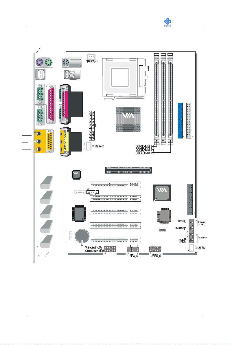
1-5 SY-7VDA MOTHERBOARD LAYOUT
PS/2 KB
PS/2 Mouse
Connector
Connector
USB 1
USB 2
PRT
COM 1
ATX Power
COM 2
AGAME
AOUT
AIN
AMIC
WOL
VT1611A
14
CDIN1
Winbond
W83697HF
-AW
1
3
Battery
CDIN2
PCI Slot #2
®
®
MX
3
1
Back Panel
SY-7VDA Platform
6
Page 11
Motherboard Description SY-7VDA
SDRAM
SDRAM
ABCDEFGHIJKLM
NOP
Q
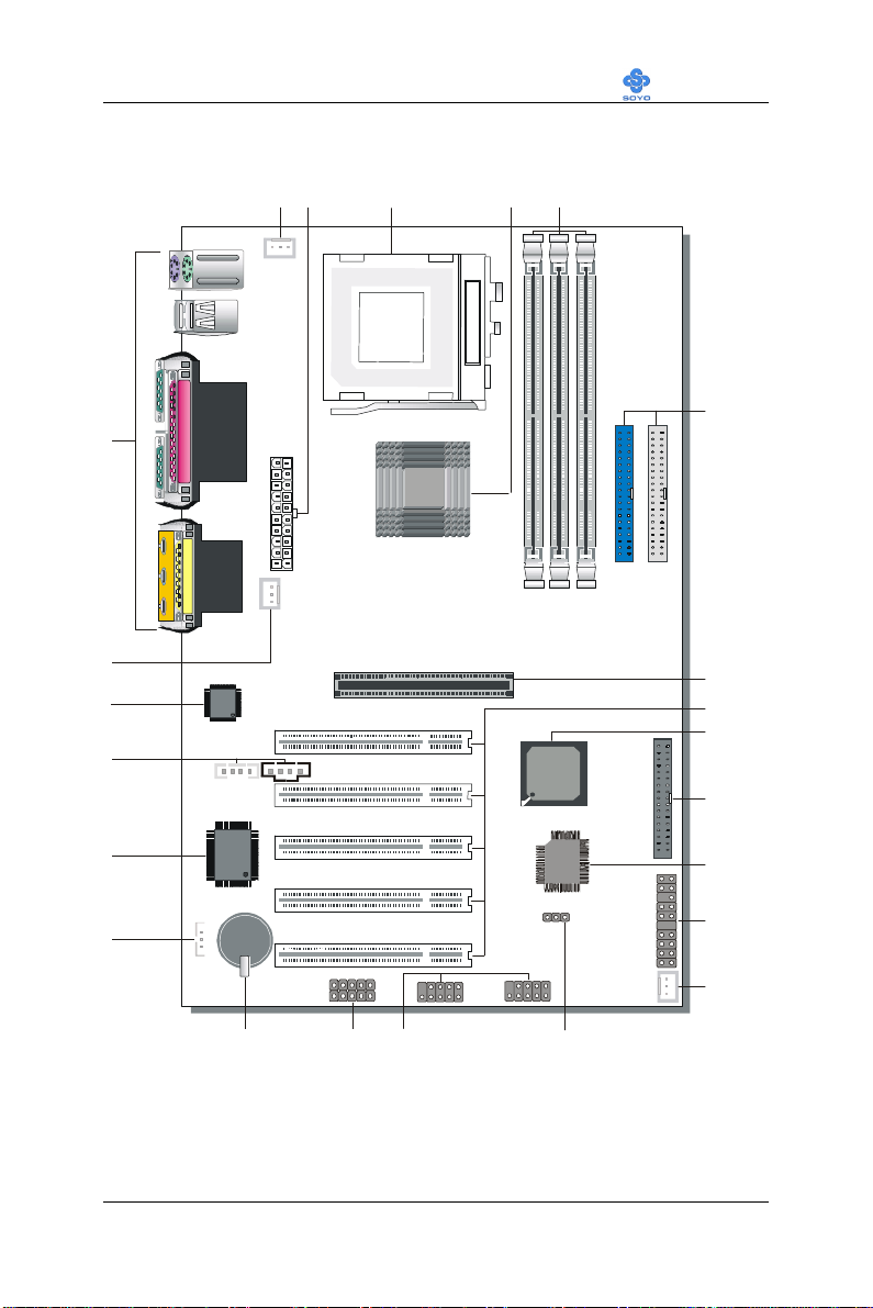
1-6 SY-7VDA MOTHERBOARD COMPONENTS
W
®
V
U
T
S
R
®
7
Page 12

Motherboard Description SY-7VDA
A CPU Cooling Fan Connector
B ATX Power Supply Connector
C Socket 370 Connector
D Via VT8633 North Bridge chip
E DDR DIMM Banks
F Bus Mastering e-IDE/ATAPI Ports
G 32-bit AGP Slot
H 32-bit PCI Mastering Slots
I Via VT8233 South Bridge Chip
J Floppy Disk Drive (FDD) Port
K Flash BIOS
L Front panel connectors
M Chassis Cooling Fan
N CMOS Clear Jumper
O USB Ports
P Serial Infrared (IrDA) Device Header
Q 3V Lithium Battery
R Wake-On-LAN (WOL) Header
S Winbond W83697HF-AW LPC I/O Chip
T CD-IN Connectors
U Via VT1611A
V Chassis Cooling Fan
W Back panel Connectors
8
Page 13

Motherboard Description SY-7VDA
1-7 MICROPROCESSOR
The motherboard supports a single Socket 370 processor. The processor’s
VID pins automatically program the voltage regulator on the motherboard
to the required processor voltage. In addition, the front side bus speed (100
MHz and 133 MHz) is automatically selected. The motherboard supports
all current Socket 370 processor speeds, voltages, and bus frequencies.
1-7.1 Microprocessor Packaging
The CPU is packaged in a 370 pin PGA package. A fan must be used to
ensure adequate cooling.
1-7.2 Second Level Cache
The second-level cache is located on the substrate of the CPU package.
The cache includes 0KB/128KB or 512 KB of synchronous pipelined
burst static RAM. All supported onboard memory can be cached.
1-7.3 Microprocessor Upgrades
The motherboard can be upgraded with Socket 370 processors that run at
higher speeds. When upgrading the processor, use the BIOS configuration
mode to change the processor speed.
9
Page 14

Motherboard Description SY-7VDA
1-8 MEMORY
1-8.1 Main Memory
The motherboard has three DDR DIMM sockets. DDR RAM can be
installed in one, two, or three sockets. Using the serial presence detect
(SPD) data structure, programmed into an E²PROM on the DDR DIMM,
the BIOS can determine the DDR RAM’s size and speed. Minimum DDR
DIMM memory size is 64 MB; maximum DDR DIMM memory size is
256/512 MB. Memory size and speed can vary between sockets.
The motherboard supports the following memory features:
− DRAM interface synchronous with host CPU (66/100/133 MHz) or
AGP (66MHz) for most flexible configuration
− DRAM interface may be faster than CPU by 33 MHz to allow use of
PC1600/2100 memory modules with 66MHz
Celeron or use of PC1600/2100 with 100MHz Pentium II or Pentium III
− Concurrent CPU, AGP, and PCI access
− Supports DDR RAM memory types only
− Flexible row and column addresses. 64-bit data width only
− 2.5V SSTL-2 DRAM interface for DDR RAM
− Optional bank-by-bank ECC (single-bit error correction and multi-bit
error detection) or EC (error checking only) for DRAM integrity
− Supports maximum 16-bank interleave (i.e., 16 pages open
simultaneously); banks are allocated based on LRU
− Independent DDR RAM control for each bank
− Seamless DRAM command scheduling for maximum DRAM bus
utilization (e.g., precharge other banks while accessing the current bank)
− Four cache lines (16 quadwords) of CPU to DRAM write buffers
− Four cache lines of CPU to DRAM read prefetch buffers
− Read around write capability for non-stalled CPU read
− Speculative DRAM read before snoop result
− Burst read and write operation
− x-1/2-1/2-1/2-1-1/2-1/2-1/2 back-to-back accesses for DDR SDRAM
10
Page 15

Motherboard Description SY-7VDA
− Supports DDR SDRAM CL 2/2.5/3 and 1T/per command
− Decoupled and burst DRAM refresh with staggered RAS timing.
− CAS before RAS or self refresh
1-9 CHIPSET
Ø VT8633
The Pro266 chipset is a high performance, cost-effective and energy
efficient chip set for the implementation of AGP / V-Link / PCI / LPC
desktop personal computer systems from 66 MHz, 100 MHz and 133 MHz
based on 64-bit Socket-370 and Slot-1 (Intel Pentium-III and Celeron)
super-scalar processors.
The Pro266 chip set consists of the VT8633 V-Link DDR Host system
controller (552 pin BGA) and the VT8233 highly integrated V-Link Client
PCI/LPC controller (376 pin BGA). The Host system controller provides
superior performance between the CPU, DRAM, AGP bus, and V-Link
interface with pipelined, burst, and concurrent operation. The VT8233 VLink Client controller is a highly integrated PCI / LPC controller. Its
internal bus structure is based on 66 MHz PCI bus that provides 2x
bandwidth compare to previous generation PCI/ISA bridge chips. The
VT8233 integrated Client V-Link controller with 266MB/S bandwidth
between Host/Client V-Link interface, provides a V-Link-PCI and VLink-LPC controller. It supports five PCI slots arbitration and decoding for
all integrated functions and LPC bus.
The VT8633 supports eight banks of SDR / DDR SDRAMs up to 4 GB.
The DRAM controller supports standard Synchronous DRAM (SDRAM),
and Virtual Channel SDRAM (VC SDRAM or VCM) SDRAM in a
flexible mix / match manner, or it can be configured to support DoubleData-Rated (DDR) SDRAM mode. The SDR/DDR DRAM interface
allows zero wait state bursting between the DRAM and the data buffers at
66 / 100 / 133 MHz. The eight banks of DRAM can be composed of an
arbitrary mixture of 1M / 2M / 4M / 8M / 16M / 32M / 64M xN DRAMs.
The DRAM controller also supports optional ECC (single-bit error
11
Page 16

Motherboard Description SY-7VDA
correction and multi-bit detection) or EC (error checking) capability
separately selectable on a bank-by-bank basis. The DRAM controller can
run either synchronous or pseudo-synchronous mode with the host CPU
bus frequency (66 / 100 / 133 MHz).
The VT8633 Host system controller also supports full AGP v2.0 capability
for maximum bus utilization including 2x and 4x mode transfers, SBA
(SideBand Addressing), Flush/Fence commands, and pipelined grants. An
eight level request queue plus a four level post-write request queue with
thirty-two and sixteen quadwords of read and write data FIFO's
respectively are included for deep pipelined and split AGP transactions. A
single-level GART TLB with 16 full associative entries and flexible CPU /
AGP / PCI remapping control is also provided for operation under
protected mode operating environments. Both Windows-95 VXD and
Windows-98 / NT5 miniport drivers are supported for interoperability with
major AGP-based 3D and DVD-capable multimedia accelerators.
The VT8633 Host system controller supports two 32-bit 3.3 system buses
(one AGP and one V-Link) that are synchronous / pseudo-synchronous to
the CPU bus. The chip also contains a built-in bus-to-bus bridge to allow
simultaneous concurrent operations on each bus. Five levels (doublewords)
of post write buffers are included to allow for concurrent CPU and V-Link
operation. For V-Link Host operation, forty-eight levels (doublewords) of
post write buffers and sixteen levels (doublewords) of prefetch buffers are
included for concurrent V-Link bus and DRAM / cache accesses. When
combined the V-Link Host/Client controllers, it realizes a complete PCI
sub-system and supports enhanced PCI bus commands such as MemoryRead-Line, Memory-Read-Multiple and Memory-Write-Invalid commands
to minimize snoop overhead. In addition, advanced features are supported
such as snoop ahead, snoop filtering, L1 write-back forward to PCI master,
and L1 write-back merged with PCI post write buffers to minimize PCI
master read latency and DRAM utilization. Delay transaction and read
caching mechanisms are also implemented for further improvement of
overall system performance.
12
Page 17

Motherboard Description SY-7VDA
The 352-pin Ball Grid Array VT8233 Client V-Link PCI / LPC controller
supports four levels (doublewords) of line buffers, type F DMA transfers
and delay transaction to allow efficient PCI bus utilization and (PCI-2.2
compliant). The VT8233 integrated PCI controller and PCI arbitration for
up to five PCI slots. One of the PCI REQ / GNT pair can be configured as
high-priority to better support a low latency PCI bus master device. The
VT8233 integrated networking MAC controller with standard MII
interface to an external PHY for 10 / 100Mb base-T Ethernet or 1 / 10Mb
PNA home networking.
The VT8233 also includes an integrated keyboard controller with PS2
mouse support, integrated DS12885 style real time clock with extended
256 byte CMOS RAM, integrated master mode enhanced IDE controller
with full scatter / gather capability and extension to UltraDMA-33/66/100
for 33/66/100 MB/sec transfer rate, integrated USB interface with root
hubs and six function ports with built-in physical layer transceivers,
Distributed DMA support, and OnNow / ACPI compliant advanced
configuration and power management interface.
For sophisticated power management, the Pro266 chipset provides
independent clock stop control for the CPU / SDRAM, PCI, and AGP
buses and Dynamic CKE control for powering down of the SDRAM. A
separate suspend-well plane is implemented for the SDRAM control
signals for Suspend-to-DRAM operation. Coupled with the VT8233 south
bridge chip, a complete power conscious PC main board can be
implemented with no external TTLs.
The Pro266 chipset is ideal for high performance, high quality, high
energy efficient and high integration desktop and notebook AGP / PCI /
LPC computer systems.
Ø VT8233
The VT8233 South Bridge is a high integration, high performance, powerefficient, and high compatibility device that supports Intel and non-Intel
13
Page 18

Motherboard Description SY-7VDA
based processor to V-Link bus bridge functionality to make a complete
Microsoft PC99-compliant PCI/ISA system. In addition to complete ISA
extension bus functionality, the VT8233 includes standard intelligent
peripheral controllers:
a) IEEE 802.3 compliant 10 / 100 Mbps PCI bus master Ethernet MAC
with standard MII interface to external PHYceiver.
b) Master mode enhanced IDE controller with dual channel DMA engine
and interlaced dual channel commands. Dedicated FIFO coupled with
scatter and gather master mode operation allows high performance
transfers between PCI and IDE devices. In addition to standard PIO and
DMA mode operation, the VT8233 also supports the UltraDMA-33
standard to allow reliable data transfer rates up to 33 MB/sec throughput.
The VT8233 also supports the UltraDMA-66 / 100 standard. The IDE
controller is SFF-8038i v1.0 and Microsoft Windows-family compliant.
c) Universal Serial Bus controller that is USB v1.1 and Universal HCI
v1.1 compliant. The VT8233 includes the root hub with six function
ports with integrated physical layer transceivers. The USB controller
allows hot plug and play and isochronous peripherals to be inserted into
the system with universal driver support. The controller also implements
legacy keyboard and mouse support so that legacy software can run
transparently in a non-USB-aware operating system environment.
d) Keyboard controller with PS2 mouse support.
e) Real Time Clock with 256 byte extended CMOS. In addition to the
standard ISA RTC functionality, the integrated RTC also includes the
date alarm, century field, and other enhancements for compatibility with
the ACPI standard.
f) Notebook-class power management functionality compliant with ACPI
and legacy APM requirements. Multiple sleep states (power-on suspend,
suspend-to-DRAM, and suspend-to-Disk) are supported with hardware
automatic wake-up. Additional functionality includes event monitoring,
14
Page 19

Motherboard Description SY-7VDA
CPU clock throttling and stop (Intel processor protocol), PCI bus clock
stop control, modular power, clock and leakage control, hardware-based
and software-based event handling, general purpose I/O, chip select and
external SMI.
g) Full System Management Bus (SMBus) interface.
h) Integrated bus-mastering dual full-duplex direct-sound AC97-link-
compatible sound system.
i) Plug and Play controller that allows complete steerability of all PCI
interrupts and internal interrupts / DMA channels to any interrupt
channel. One additional steerable interrupt channel is provided to allow
plug and play and reconfigurability of on-board peripherals for Windows
family compliance.
The VT8233 also enhances the functionality of the standard ISA
peripherals. The integrated interrupt controller supports both edge and
level triggered interrupts channel by channel. The integrated DMA
controller supports type F DMA in addition to standard ISA DMA modes.
Compliant with the PCI-2.2 specification, the VT8233 supports delayed
transactions and remote power management so that slower ISA peripherals
do not block the traffic of the PCI bus. Special circuitry is built in to allow
concurrent operation without causing dead lock even in a PCI-to-PCI
bridge environment. The chip also includes eight levels (doublewords) of
line buffers from the PCI bus to the ISA bus to further enhance overall
system performance.
1-10 I/O INTERFACE CONTROLLER
The motherboard uses the Winbond W83697HF LPC Super-I/O controller
which features:
Ø Supports 2 serial ports, IR port, parallel port, and floppy disk
controller functions
Ø Two UARTs for Complete Serial Ports
Even, odd, stick or no parity bit generation and detection
15
Page 20

Motherboard Description SY-7VDA
Programmable baud rate generator
High speed baud rate (230Kbps, 460Kbps) support
Independent transmit/receiver FIFOs
Modem Control
Plug and play with 96 base IO address and 12 IRQ options
Ø One dedicated IR port
Third serial port dedicated to IR function
IR function either through the two complete serial ports or the
third dedicated port
Infrared-IrDA (HPSIR) and ASK (Amplitude Shift Keyed) IR
Ø Multi-mode parallel port
Standard mode, ECP and EPP support
Plug and play with 192 base IO address, 12 IRQ and 4 DMA
options
Ø Floppy Disk Controller
16bytes of FIFO
Data rates up to 1Mbps
Perpendicular recording driver support
Two FDDs with drive swap support
Plug and play with 48 base IO address, 12 IRQ and 4 DMA
options
The Setup program provides configuration option for the I/O controller.
1-10.1 Serial Ports
The motherboard has two 9-pin D-Sub serial port connectors located on
the back panel. The NS16C5450-compatible UARTs support data transfers
at speeds up to 115.2 Kbits/sec with BIOS support.
1-10.2 Parallel Port
The connector for the multimode bi-directional parallel port is a 25-pin DSub connector located on the back panel of the motherboard. In the Setup
program, there are four options for parallel port operation:
l Compatible (standard mode)
l Bi-directional (PS/2 compatible)
16
Page 21

Motherboard Description SY-7VDA
l Bi-directional EPP. A driver from the peripheral manufacturer is
required for operation.
l Bi-directional high-speed ECP
1-10.3 Diskette Drive Controller
The I/O controller is software compatible with the 82077 diskette drive
controller and supports both PC-AT and PS/2 modes. In the Setup program,
the diskette drive interface can be configured for the following diskette
drive capacities and sizes.
l 360 KB, 5.25-inch
l 1.2 MB, 5.25-inch
l 720 KB, 3.5-inch
l 1.2 MB. 3.5-inch (driver required)
l 1.25-1.44 MB, 3.5-inch
l 2.88 MB, 3.5-inch
17
Page 22

Motherboard Description SY-7VDA
1-10.4 PS/2 Keyboard and Mouse Interface
PS/2 keyboard and mouse connectors are located on the back panel of the
motherboard. The +5 V lines to keyboard and mouse connectors are
protected with a fuse that prevents motherboard components from being
damaged when an over-current condition occurs.
Note
The mouse and keyboard can be plugged into either PS/2 connector.
Power to the computer should be turned off before a keyboard or mouse is
connected or disconnected.
The keyboard controller contains code, which provides the traditional
keyboard and mouse control functions, and also supports Power On/Reset
password protection. Power On/Reset password can be specified in the
BIOS Setup program.
The keyboard controller also supports the hot-key sequence
<Ctrl><Alt><Del>, software reset. This key sequence resets the
computer’s software by jumping to the beginning of the BIOS code and
running the Power On Self Test (POST).
1-10.5 Infrared Support
On the front panel I/O connector, there are six pins that support Hewlett
Packard HSDL-1000 compatible infrared (IR) transmitters and receivers.
In the Setup program, Serial Port B can be direct4d to a connected IR
device. (In this case, the Serial Port B connector on the back panel cannot
be used.) The IR connection can be used to transfer files to or from
portable devices like laptops, PDAs, and printers. The Infrared Data
Association (IrDA) specification supports data transfers of 115Kbits/sec at
a distance of 1 meter.
1-11 HARDWARE MONITOR
The optional hardware monitor subsystem provides low-cost
instrumentation capabilities. The features of the hardware monitor
18
Page 23

Motherboard Description SY-7VDA
subsystem include:
Ø An integrated ambient temperature sensor
Ø Fan speed sensors, which monitor the fan 1 and fan 2 connector.
Ø Power supply voltage monitoring to detect levels above or below
acceptable values
When suggested ratings for temperature, fan speed, or voltage are
exceeded, an interrupt is activated. The hardware monitor component
connects to the SMBus.
1-12 WAKE ON LAN TECHNOLOGY
Wake on LAN technology enables remote wakeup of the computer
through a network. Wake on LAN technology requires a PCI add-in
network interface card (NIC) with remote wakeup capabilities. The remote
wakeup connector on the NIC must be connected to the onboard Wake on
LAN connector. The NIC monitors network traffic at the Ethernet
interface; upon detecting a Magic Packet, the NIC asserts a wakeup signal
that powers up the computer. This feature uses the Wake on LAN
connector.
*
CAUTION
For Wake on LAN, the 5-V standby line for the power supply must be
capable of delivering +5V ±5 % at 720 mA. Failure to provide adequate
standby current when implementing Wake on LAN can damage the power
supply.
19
Page 24

BIOS Setup Utility SY-7VDA
Chapter 2
HARDWARE INSTALLATION
Congratulations on your purchase of SY-7VDA Motherboard. You are
about to install and connect your new Motherboard.
Note: Do not unpack the Motherboard from its protective antistatic packaging until you have made the following preparations.
2-1 PREPARATIONS
Gather and prepare all the following hardware equipment to complete the
installation successfully:
1. Socket 370 processor with built-in CPU cooling fan (boxed type).
Note: This Motherboard supports non-boxed type CPUs. The heavier
CPU cooling fan requires the installation of a CPU support stand.
2. DDR RAM module (s)
3. Computer case and chassis with adequate power supply unit
4. Monitor
5. PS/2 Keyboard
6. Pointing Device (PS/2 mouse)
7. Speaker(s) (optional)
8. Disk Drives: HDD, CD-ROM, Floppy drive…
9. External Peripherals: Printer, Plotter, and Modem (optional)
10. Internal Peripherals: Modem and LAN cards (optional)
20
Page 25
BIOS Setup Utility SY-7VDA
2-2 UNPACKING THE MOTHERBOARD
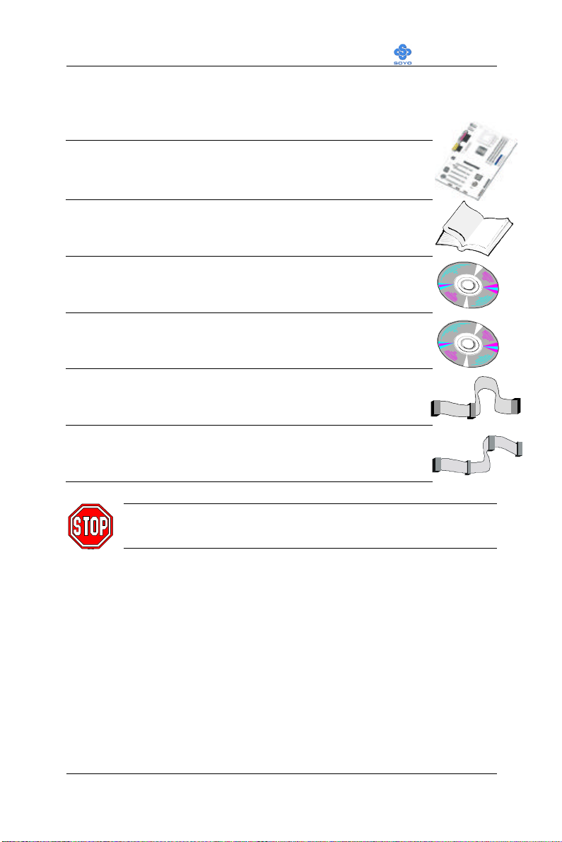
When unpacking the Motherboard, check for the following items:
u The SY-7VDA PRO266 AGP/PCI Motherboard
u The Quick Start Guide
u The Installation CD-ROM
u SOYO Bonus Pack CD-ROM
u One IDE Device ATA 66 Flat Cable
u One Floppy Disk Drive Flat Cable
Warning: Do not unpack the Motherboard from its anti-static
packaging until you are ready to install it.
Like most electronic equipment, your Motherboard may be damaged by
electrostatic discharge. To avoid permanent damage to components ground
yourself while working by using a grounding strap. Otherwise, ground
yourself frequently by touching the unpainted portion of the computer
chassis to drain the static charges.
Handle the Motherboard carefully, holding it by the edges.
You are now ready to start the installation.
21
Page 26

BIOS Setup Utility SY-7VDA
2-3 INSTALLATION GUIDE
We will now begin the installation of the Motherboard. Please follow the
step-by-step procedure designed to lead you to a complete and correct
installation.
Warning: Turn off the power to the Motherboard, system chassis,
and peripheral devices before performing any work on the
Motherboard or system.
BEGIN THE INSTALLATION
22
Page 27
BIOS Setup Utility SY-7VDA
2-3.1 CPU Installation
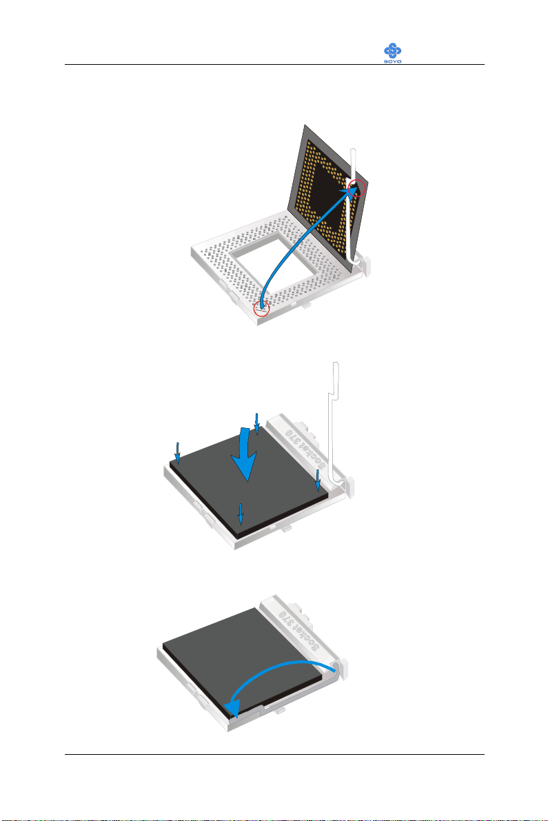
Your SY-7VDA motherboard comes with a CPU retention set kit. The
retention set is used to hold the processor attached to the Socket 370 CPU
connector on the motherboard.
Mark your CPU Frequency:
your CPU that should be clearly marked on the CPU cover.
Record the working frequency of
FSB 66MHz
400MHz (66 x 6.0) 466MHz (66 x7.0) 533MHz (66 x 8.0) 600MHz (66 x 9.0) 667MHz (66 x 10.0)
433MHz (66 x 6.5) 500MHz (66 x7.5) 566MHz (66 x 8.5) 633MHz (66 x 9.5) 700MHz (66 x 10.5)
FSB 100MHz
500MHz (100 x 5.0) 600MHz (100 x 6.0) 700MHz (100 x 7.0) 800MHz (100 x 8.0)
550MHz (100 x 5.5) 650MHz (100 x 6.5) 750MHz (100 x7.5) 850MHz (100 x 8.5)
FSB 133MHz
533MHz(133x4.0) 667MHz(133x5.0) 800MHz(133x 6.0) 933MHz(133x 7.0) 1.13GHz(133x 8.5)
600MHz(133x4.5) 733MHz(133x5.5) 866MHz(133x 6.5) 1000MHz(133x 7.5)
CPU Mount Procedure:
processor & VIA Cyrix processor that you have purchased separately, follow
these instructions.
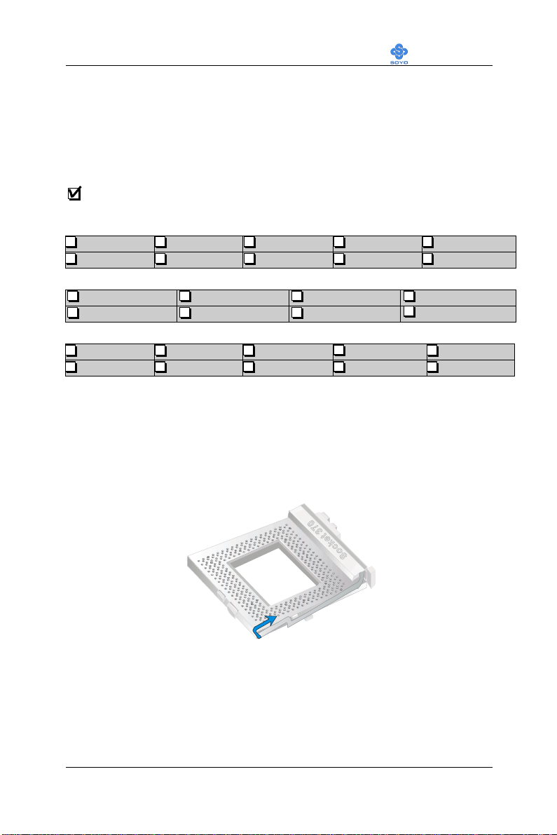
To mount the Pentium® & Celeron
TM
1. Lift the socket handle up to a vertical position.
23
Page 28
BIOS Setup Utility SY-7VDA
2. Align the blunt edge of the CPU with the matching pinhole distinctive
edge on the socket.
3. Seat the processor in the socket completely and without forcing.
4. Then close the socket handle to secure the CPU in place.
24
Page 29

BIOS Setup Utility SY-7VDA
Remember to connect the CPU Cooling Fan to the
appropriate power connector on the Motherboard. The fan is
a key component that will ensure system stability. The fan
prevents overheating, therefore prolonging the life of your
CPU.
2-3.1.1 CPU Fan Installation
Your Socket 370 processor kit comes with a cooling fan. Mount the fan on
the processor according to the instructions provided by the manufacturer.
The fan is a key component that will ensure system stability. The fan
prevents overheating, therefore prolonging the life of your CPU.
Note: Remember to connect the fan to the appropriate power source.
25
Page 30
BIOS Setup Utility SY-7VDA
SDRAM
SDRAM
1
92
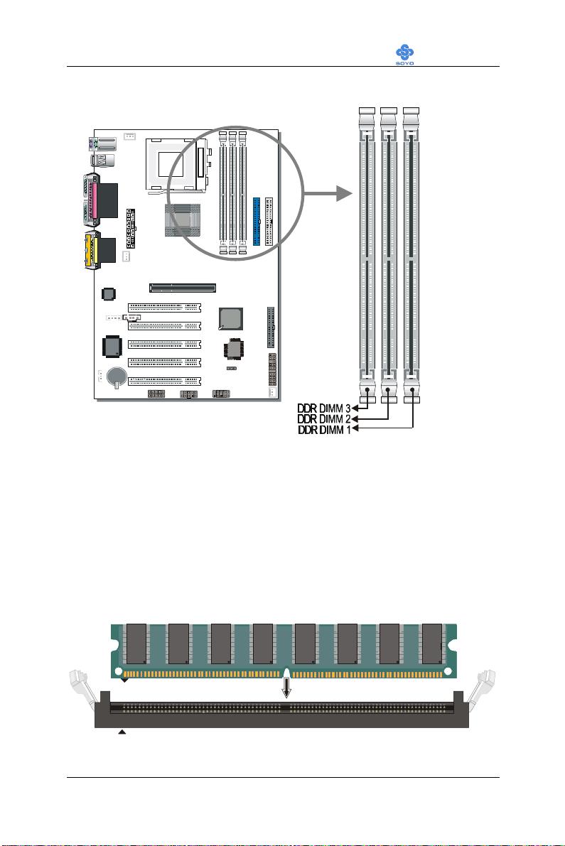
2-3.2 DDR RAM Memory Module Installation
®
®
Your board comes with three DIMM sockets, providing support for up to
3GB of main memory using unbuffered and registered DIMM modules
from 64MB to 1GB. On this motherboard, DRAM speed can be set
independent from the CPU front side bus speed. Depending on the DRAM
clock speed setting in the BIOS setup (Chapter 3), appropriate memory
modules must be used. For 100MHz DRAM speed, use PC1600 memory;
for 133MHz DRAM speed, use PC2100 memory.
1
92
26
Page 31

BIOS Setup Utility SY-7VDA
Memory Configuration Table
Number of Memory
Modules
RAM Type
Memory Module Size
(MB)
DIMM 1 DIMM 2 DIMM 3
DDR RAM
64 / 128 / 256 / 512 / 1024 MB
27
Page 32
BIOS Setup Utility SY-7VDA
SDRAM
SDRAM
IDE 2
IDE 1
Pin -1
IDE
39
39
40-pin
80-Conductor
2-3.3 Motherboard Connector
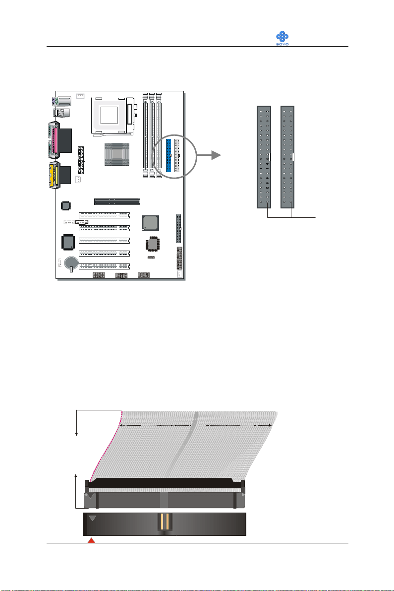
2-3.3.1 IDE Device Installation (HDD, CD-ROM)
®
®
Primary
This Motherboard offers two primary and secondary IDE device
connectors (IDE1, IDE2). It can support up to four high-speed Ultra DMA
33/66/100HDD or CD-ROM.
Secondary
IDE
Connect one side of the ATA66/100 flat cable to the IDE device (HDD or
CD-ROM) and plug the other end to the primary (IDE1) or secondary
(IDE2) directionally keyed IDE connector on the Motherboard. The
ATA66/100 cable is backward compatible with ATA33 HDDs.
This Motherboard can support up to four HDDs.
ATA 66/100
Flat Cable
1
1
28
Page 33
BIOS Setup Utility SY-7VDA
SDRAM
SDRAM
33
33
Pin -1
Floppy Drive
Connector
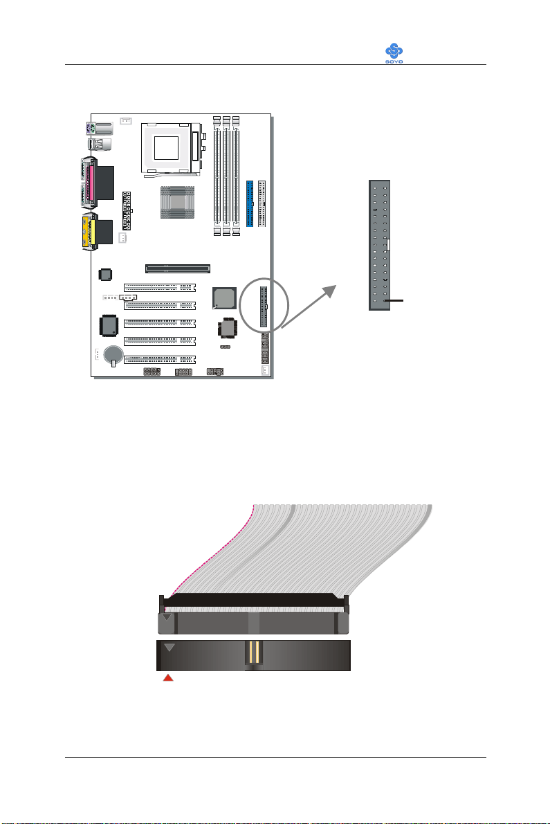
2-3.3.2 Floppy Drive Installation
®
®
FDC
The system supports 5 possible floppy drive types: 720 KB, 1.2 MB,
1.44 MB, 2.88 MB, and LS-120.
Connect one side of the 34-pin flat cable to the floppy drive and plug the
other end to the floppy drive connector on the Motherboard.
This Motherboard can support up to 2 floppy drives.
1
1
29
Page 34
BIOS Setup Utility SY-7VDA
SDRAM
SDRAM
Power
Key Lock
Power LED
Pin Assignment
GND
2-3.3.3 Front Panel Connections
_
_
+
LED
+
Speaker
®
®
Reset
PWRBT
STR
LED
HDD
LED
_
_
+
+
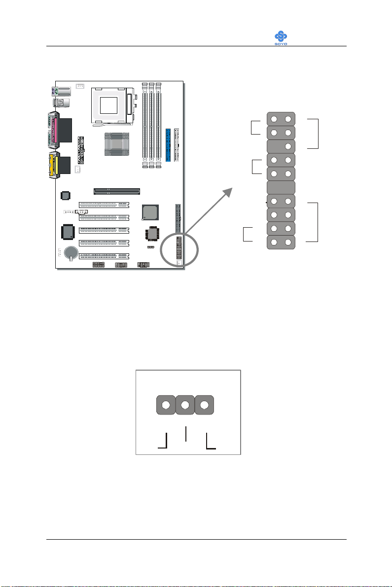
Plug the computer case's front panel devices to the corresponding headers
on the Motherboard.
1. Power LED
Please install according to the following pin assignment: pin 1,3 are for
Power LED.
+5V+5V
+
_
NCNC
30
Page 35
BIOS Setup Utility SY-7VDA
Reset Pin Assignment
Power Good
GND
Speaker Pin Assignment
Speaker out
HDD LED Pin Assignment
LED Anode
LED Cathode
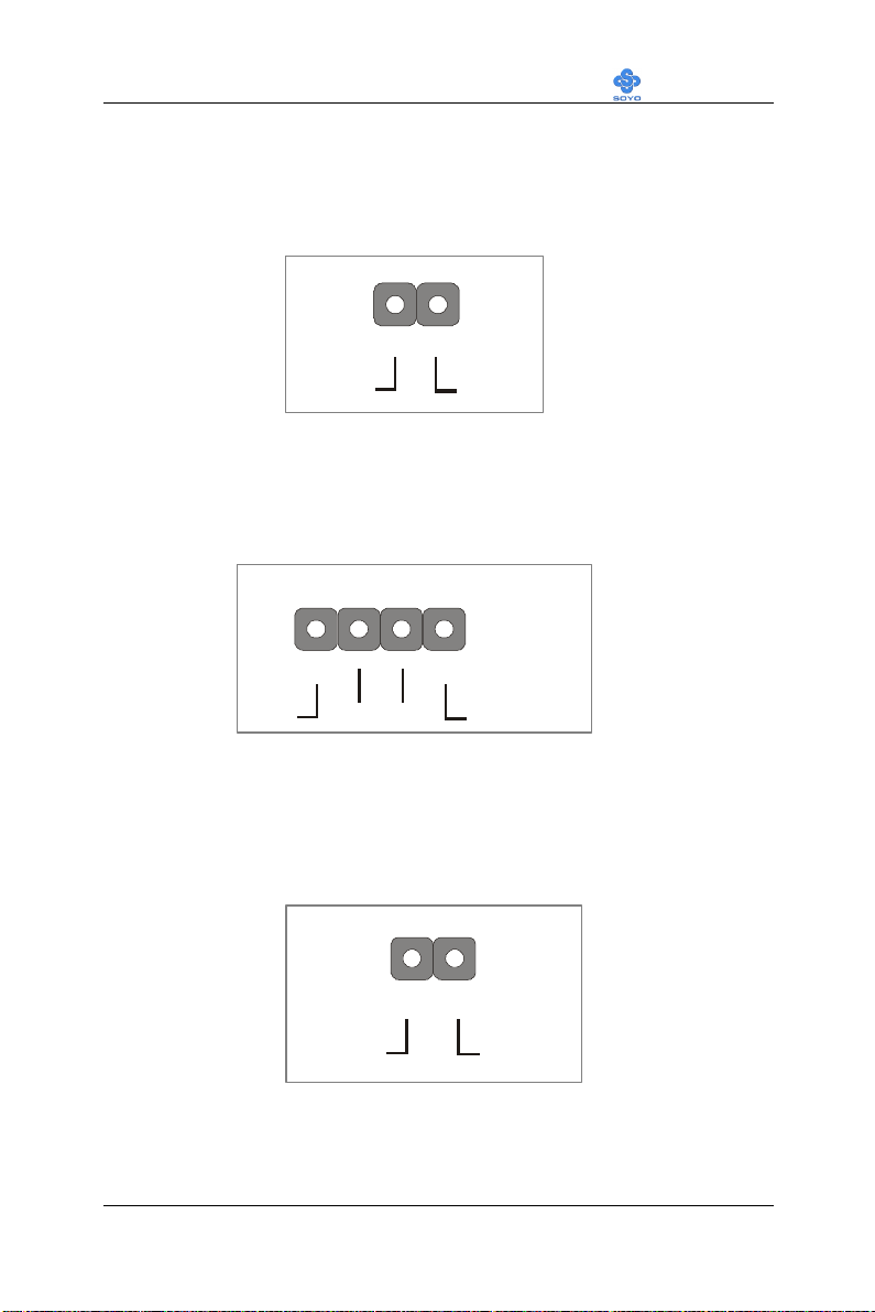
2. Reset
Plug the Reset push-button cable into the 2-pin Reset header on the
Motherboard. Pushing the Reset button on the front panel will cause the
system to restart the boot-up sequence.
1
3. Speaker
Attach the 4-pin PC speaker cable from the case to the Speaker header on
the Motherboard.
_
+
+5V
4. IDE LED
Attach the 2-pin IDE device LED cable to the corresponding IDE LED
header on the Motherboard. This will cause the LED to light up when an
IDE (HDD, CD-ROM) device is active.
NC NC
+
_
31
Page 36
BIOS Setup Utility SY-7VDA
SDRAM
SDRAM
PWRBT Pin Assignment
Power On/Off
GND
PRT
PS/2 Mouse
AMIC
AGAME
USB 2
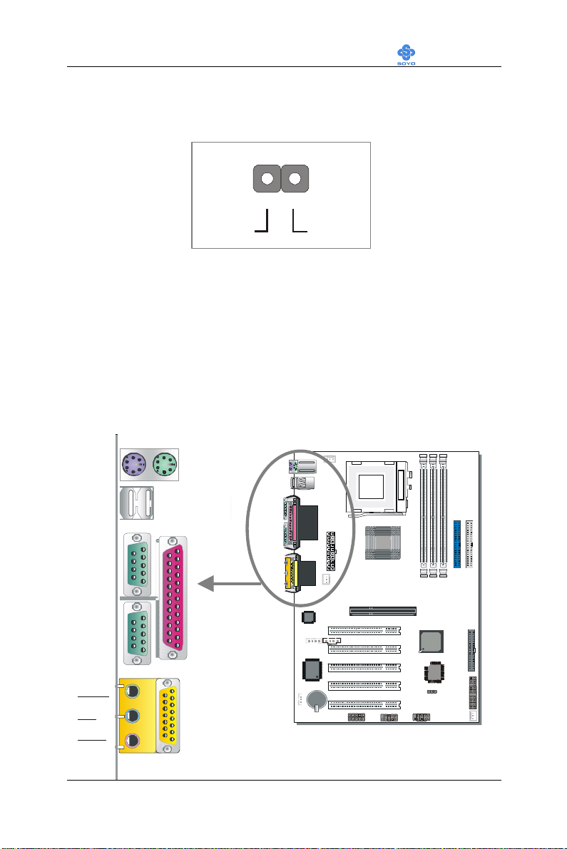
5. ATX Power On/Off Switch
Attach the 2-pin momentary type switch to the PWRBT header for turning
On or Off your ATX power supply.
1
2-3.3.4 Back Panel Connections
All external devices such as the PS/2 keyboard, PS/2 mouse, printer,
modem, USB can be plugged directly onto the Motherboard back panel.
Only after you have fixed and locked the Motherboard to the computer
case can you start connecting the external peripheral devices.
When connecting an external device, use the following figure to locate and
identify which back panel connector to plug the device to.
PS/2 KB
Connector
Connector
USB 1
COM 1
COM 2
AOUT
AIN
32
®
®
Page 37
BIOS Setup Utility SY-7VDA
Pin5
KBD Clock
Pin5
Mouse Clock
1. Onboard Serial Ports COM1/COM2
External peripherals that use serial transmission scheme include:
- serial mouse,
- and modem.
Plug the serial device cables directly into the COM1/COM2 9-pin male
connectors located at the rear panel of the Motherboard.
2. Parallel Port PRT
This parallel port is used to connect the printer or other parallel devices.
Plug the parallel device cable into the 25-pin female connector located at
the rear panel of the Motherboard.
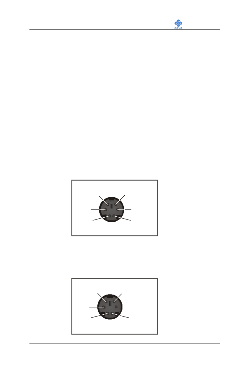
3. PS/2 Keyboard
Plug the keyboard jack directly into the 6-pin female PS/2 keyboard
connector located at the rear panel of the Motherboard.
Pin6
NC
Pin4
VCC
Pin2
NC
Pin3
GND
Pin1
KBD DATA
4. PS/2 Mouse
Similarly, plug the mouse jack directly into the 6-pin female PS/2 mouse
connector.
Pin6
NC
Pin4
VCC
Pin2
NC
Pin3
GND
Pin1
Mouse DATA
33
Page 38
BIOS Setup Utility SY-7VDA
1
5
2
3
4
(+)Data
(-)Data
USB4
1
5
2
3
4
(+)Data
(-)Data
USB6
USB5
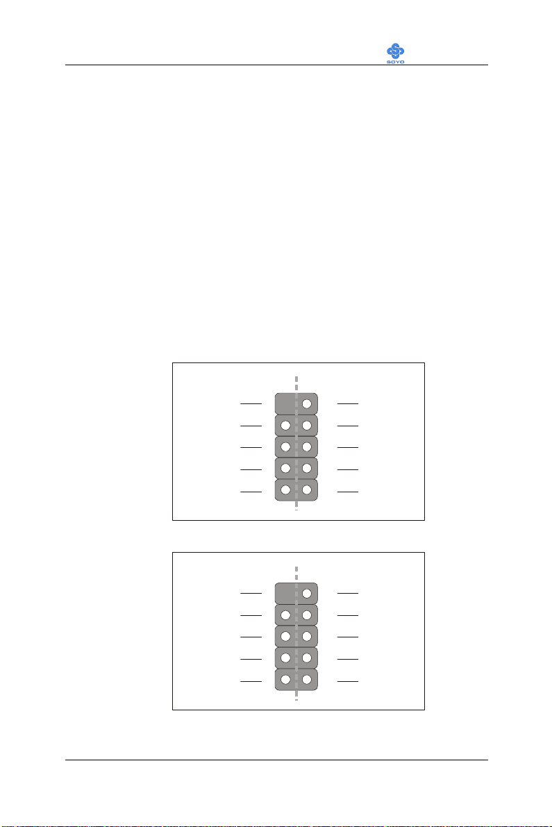
5. Universal Serial Bus USB1/USB2 (USB3/USB4¡FUSB5/USB6)
This Motherboard provides four USB ports for your additional devices.
Plug the USB device jack into the available USB connector USB1 or
USB2.
- Standard device drivers come with the Win98 for commonly used
USB devices.
- With Win95, use the flow UHCI specifications. To use USB devices
under Win95, usually you have to install the device that driver comes
with the USB device you have purchased.
USB3, USB4, USB5 and USB6 are available. To make use of these USB
ports, purchase a USB cable from your dealer. The lay-out of USB3/USB4
and USB5/USB6 are as follows:
USB3
GND
GND
(+)Data
(-)Data
Power
5
4
3
2
1
GND
GND
Power
GND
GND
(+)Data
(-)Data
Power
5
4
3
2
1
34
GND
GND
Power
Page 39

BIOS Setup Utility SY-7VDA
6. Onboard Game port/audio
This Motherboard provides Joystick port and audio.
- Attach the joystick cable to the 15-pin GAME port at the rear panel
of you motherboard.
- This Motherboard features three built-in audio-stereo ports (labeled
line-in, line-out, and mic jack) convenient to directly plug-in all your
external audio devices.
35
Page 40
BIOS Setup Utility SY-7VDA
Wake-On-LAN
JP10 Pin Assignment
MP-Wake-up
2-3.3.5 Other Connections
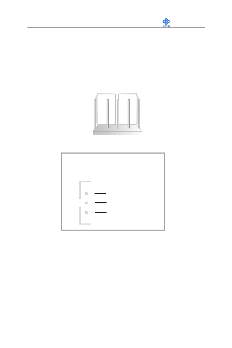
1. Wake-On-LAN (WOL)
Attach the 3-pin connector from the LAN card which supports the WakeOn-LAN (WOL) function to the JP10 header on the Motherboard. This
WOL function lets users wake up the connected computer through the
LAN card.
Please install according to the following pin assignment:
1
2
3
5VSB
GND
36
Page 41
BIOS Setup Utility SY-7VDA
3
4
5
IRRX
IRTX
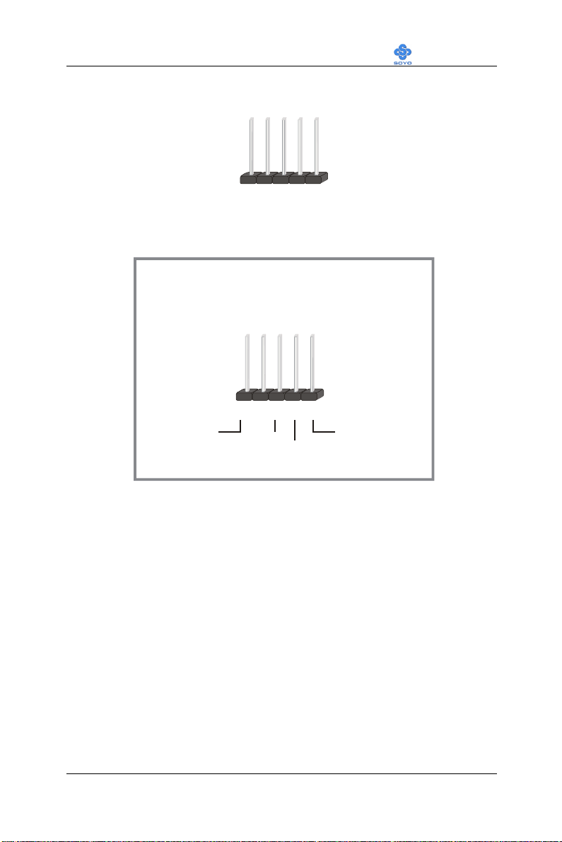
2. Standard Infrared (SIRCON)
Plug the 5-pin infrared device cable to the SIRCON header. This will
enable the infrared transfer function. This Motherboard meets both the
ASKIR and HPSIR specifications.
Please install according to the following pin assignment:
Standard Infrared
(SIRCON) Connector
SIRCON Pin Assignment
12
VCC
GND
37
Page 42
BIOS Setup Utility SY-7VDA
CPU Cooling Fan
CPUFAN Pin Assignment
SENSOR
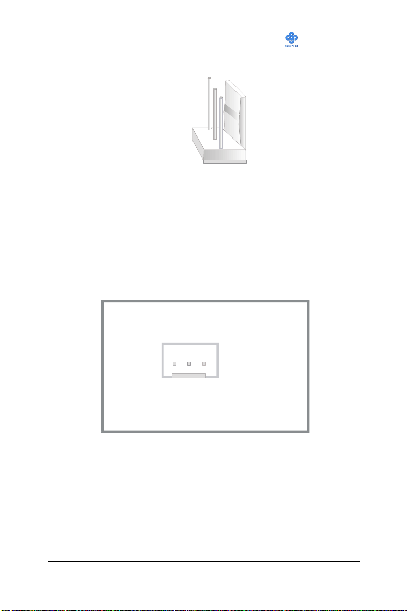
3. Cooling Fan Installation
(1) CPU Cooling Fan
After you have seated the CPU properly on the processor, attach the 3-pin
fan cable to the CPUFAN connector on the Motherboard. The fan will stop
when the system enters into Suspend Mode. (Suspend mode can be
enabled from the BIOS Setup Utility, [POWER MANAGEMENT] menu.)
To avoid damage to the system, install according to the following pin
assignment:
132
12VGND
38
Page 43
BIOS Setup Utility SY-7VDA
SENSOR
CHAFAN2
CHAFAN1
SENSOR
Chassis Cooling Fan
CHAFAN Pin Assignment
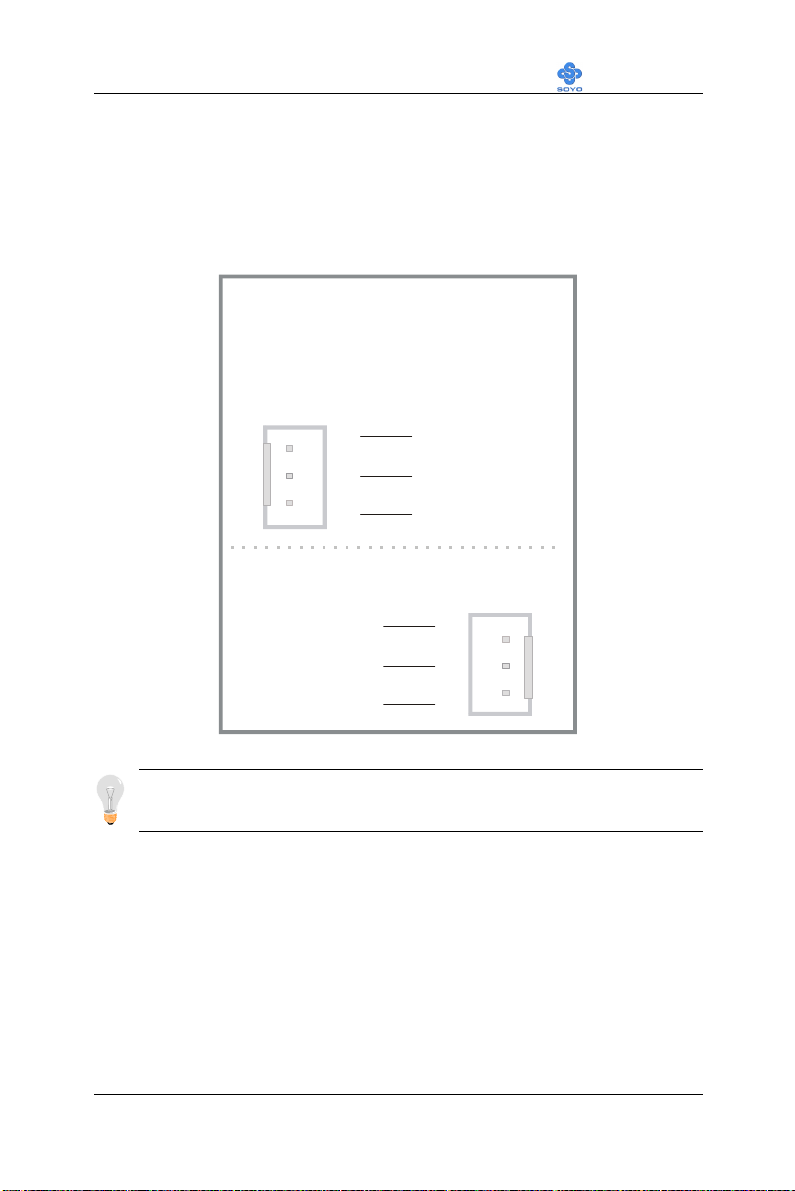
(2) Chassis Cooling Fan (CHAFAN1,CHAFAN2)
Some chassis also feature a cooling fan. This Motherboard features a
CHAFAN connector to provide 12V power to the chassis fan. Connect the
cable from the chassis fan to the CHAFAN 3-pin connector. Install
according to the following pin assignment:
(CHAFAN1,CHAFAN2)
GND1
2
12V
3
3
12V
2
GND 1
Note: CPUFAN must be installed for this Motherboard, CHAFAN is
optional.
39
Page 44
BIOS Setup Utility SY-7VDA
Pin Assigment
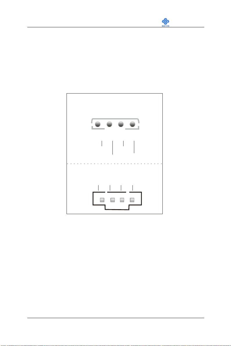
4. CD Line-in (CDIN1,CDIN2)
This Motherboard provides two CD-Line in connectors. Please connect the
4-pin audio cable from your CD-ROM drive to either CDIN1 or CDIN2.
(It fits in only one, depending on the cable that came with your CD-ROM
drive)
Please install according to the following pin assignment:
CDIN1,CDIN2(CD Line-in)
1
CDIN1
Right
Right
4433221
GND
Left
GNDGND
GND
Left
CDIN2
2-3.3.6 AGP VGA Card
Insert the AGP VGA card into the AGP slot. Then connect the monitor
information cable to the AGP card back plane external connector.
Follow the manufacturer's instructions to perform the AGP VGA drivers
installation.
40
Page 45
BIOS Setup Utility SY-7VDA
SDRAM
SDRAM
ATX Power
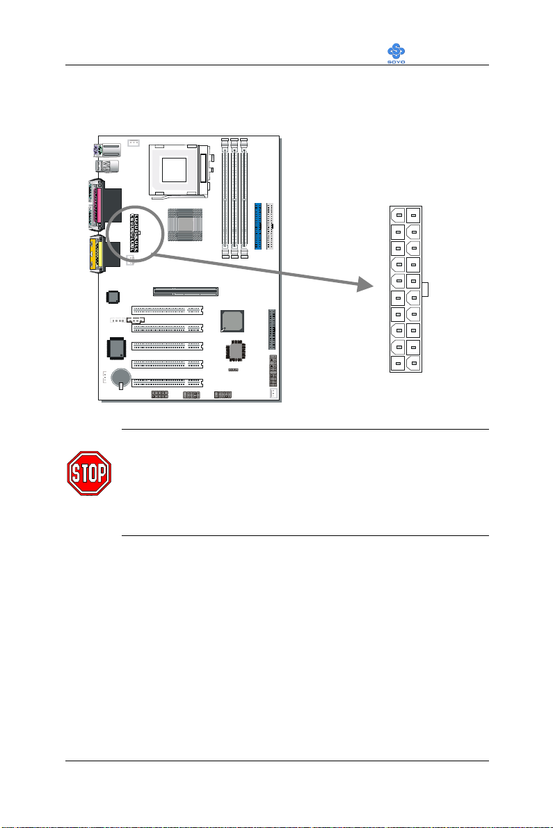
2-3.3.7 ATX Power Supply
Plug the connector from the power directly into the 20-pin male ATX PW
connector on the Motherboard, as shown in the following figure.
®
®
Warning: Follow these precautions to preserve your
Motherboard from any remnant currents when connecting to
ATX power supply:
Turn off the power supply and unplug the power cord of the
ATX power supply before connecting to ATX PW connector.
The Motherboard requires a power supply with at least 200 Watts and a
"power good" signal. Make sure the ATX power supply can take at least
720 mA * load on the 5V Standby lead (5VSB) to meet the standard ATX
specification.
* Note: If you use the Wake-On-LAN (WOL) function, make sure the
ATX power supply can support at least 720 mA on the 5V Standby lead
(5VSB).
41
Page 46
BIOS Setup Utility SY-7VDA
3.3V
-12V
PS-ON
ATX Power
123
123
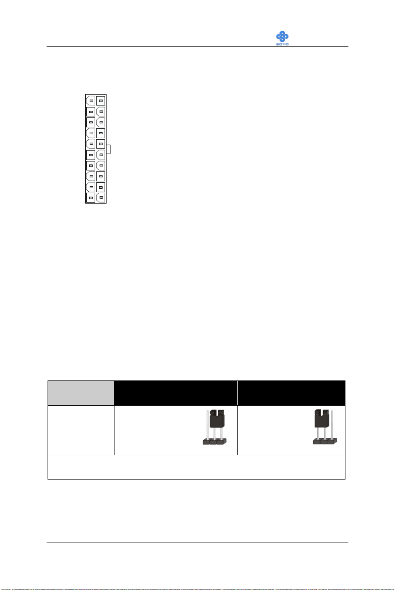
Please install the ATX power according to the following pin assignment:
12V
5VSB
PW-OK
GND
5V
GND
5V
GND
3.3V
3.3V
5V
5V
-5V
GND
GND
Ø Pay special care to the directionality.
GND
GND
2-3.4 CMOS Clear (JP5)
In some cases the CMOS memory may contain wrong data, follow the
steps below to clear the CMOS memory.
1. Clear the CMOS memory by momentarily shorting pin 2-3 on jumper
JP5. This jumper can be easily identified by its white colored cap.
2. Then put the jumper back to 1-2 to allow writing of new data into the
CMOS memory.
Clearing
JP5 Setting
Note: You must unplug the ATX power cable from the ATX power
connector when performing the CMOS Clear operation.
CMOS
Clear CMOS Data Retain CMOS Data
Short pin 2-3 for
at least 5 seconds
to clear the CMOS
Short pin 1-2 to
retain new
settings
42
Page 47

BIOS Setup Utility SY-7VDA
2-3.5 Power On
You have now completed the hardware installation of your Motherboard
successfully.
1. Turn the power on
2. To enter the BIOS Setup Utility, press the <DEL> key while the system
is performing the diagnostic checks,
Note: If you have failed to enter the BIOS, wait until the boot up
sequence is completed. Then push the RESET button and press
<DEL> key again at the beginning of boot-up, during diagnostic
checks.
43
Page 48

BIOS Setup Utility SY-7VDA
Repeat this operation until you get the following screen.
3. The BIOS Setup screen appears:
CMOS Setup Utility – Copyright ( C ) 1984-2001 Award Software
4SOYO COMBO Feature 4PC Health Status
4Standard CMOS Features Load Optimized Defaults
4Advanced BIOS Features Load Fail - Safe Defaults
4Advanced Chipset Features Set Supervisor Password
4Integrated Peripherals Set User Password
4Power Management Setup Save & Exit Setup
4PnP/PCI Configurations Exit Without Saving
Esc : Quit áâàß : Select Item
F10 : Save & Exit Setup
Change CPU’s Clock & Voltage
2-3.6 Quick BIOS Setup
This Motherboard does not use any hardware jumpers to set the CPU
frequency. Instead, CPU settings are software configurable with the BIOS
[SOYO COMBO FEATURE]. The [SOYO COMBO FEATURE]
combines the main parameters that you need to configure, all in one menu,
for a quick setup in BIOS.
After the hardware installation is complete, turn the power switch
on, then press the
<DEL>
key during the system diagnostic checks
to enter the Award BIOS Setup program. The CMOS SETUP
UTILITY will be shown on the screen. Then, follow these steps to
configure the CPU settings.
44
Page 49

BIOS Setup Utility SY-7VDA
Step 1. Select [STANDARD CMOS SETUP]
Set [Date/Time] and [Floppy drive type], then set [Hard Disk Type] to
“Auto”.
Step 2. Select [LOAD OPTIMIZED DEFAULTS]
Select the “LOAD OPTIMIZED DEFAULTS” menu and type “Y” at the
prompt to load the BIOS optimal setup.
Step 3. Select [SOYO COMBO FEATURE]
Set the [CPU Frequency Select] field to “Manual”, to be able to change
the CPU frequency 1 MHz stepping.
Step 4. Select [SAVE & EXIT SETUP]
Press <Enter> to save the new configuration to the CMOS memory, and
continue the boot sequence.
45
Page 50

BIOS Setup Utility SY-7VDA
2-3.7 Troubleshooting at First Start
USB Issues
Can I use USB port 3_4 and port 5_6 for keyboard resume function?
This M/B has 6 USB ports, but only the 2 at the back panel can be used for
USB keyboard resume function.
Video (no display) related issues
I built a new computer system using a Soyo board and nothing
happens when turning it on, no video and no beeps from the PC
speaker. What is happening and how can it be fixed?
No screen and no beeps mean that your CPU and motherboard do not work
at all. It could be that the CPU is not seated correctly or that a component
on the M/B is grounded (shorted) with the case. Also make sure to check
the voltage setting switch (110V/220V) on the back of the power supply.
To isolate the problem do the following:
1. Press and hold down on the “Ins” (insert) key while turning on the
computer until you get video. If you do not get video then,
2. Double-check jumpers setting on you motherboard and remove all
add-on cards, unplug all hard-disk and floppy-disk drive cables and see if
you can hear some beeps. If you still do not get any beeps, then try putting
the motherboard on the table (to isolate it from the case) with the CPU and
speaker only, and give it one more try.
I hear a series of beeps and I do not get anything from my monitor.
What could be wrong?
The following lists some basic beep codes and their possible meanings:
• One long beep and 3 very short beeps - The video card is not
detected by the motherboard. Please re-seat your video card. If
you are using an AGP card, please push your AGP card down real
hard. You may have to push VERY hard without the AGP card
mounting screw. Make sure not to insert the card the other way
around.
46
Page 51

BIOS Setup Utility SY-7VDA
• Continuous beeps – One or more of the memory modules is not
seated correctly in its socket.
My PCI VGA card works fine with my system, but when I put in a
new AGP card, it does not give me any video. Is my AGP slot bad?
This is a common problem with AGP video cards. The reason is that your
AGP card did not get seated into the AGP slot fully and firmly. Please
push your AGP card down into the socket real hard, it should snap twice.
You may have to unscrew the AGP card to allow the card to go further
down. Do take care not to damage the card by using too much force.
I get distorted video my AGP card right after I save my bios. Why is
that?
The cause is likely that your AGP card is not running at the correct bus
speed. To fix this, please clear the CMOS via JP5 and if it still does not
work, please upgrade your motherboard bios to the latest version.
BIOS Issues
Where can I find the BIOS revision of my mainboard?
It will be displayed on the up-left corner on the screen during boot-up. It
will show as your board type followed by the revision number, such as
5EH_2CA1 (meaning revision 2CA1 for the SY-5EH board) or 6BA+
IV_2AA2 which means SY-6BA+ IV motherboard with 2AA2 bios.
Where can I find the latest BIOS of my motherboard?
Please go to the technical support page of one of the SOYO websites
(Taiwan: www.soyo.com.tw), and look up your motherboard to find
the latest BIOS revision.
Hard disk, floppy drive, CD-ROM etc
When I boot up my new computer I got "floppy boot failure" and the
LED on the floppy stays on
Make sure the red wire of floppy ribbon cable goes to Pin1 on the floppy
drive side (don't trust the "key lock" or "notch") and use the end-connector
of the cable (don't use middle one).
47
Page 52

BIOS Setup Utility SY-7VDA
Modem issues
I get an "I/O Conflict" message when I turn on my system and I can
not get my modem to work
What you need to do is to disable 'COM2' (or UART2 or serial port 2) in
the bios under integrated peripheral setup.
I have installed my modem drivers several times and I still cannot get
my modem to work. Why?
If you are sure that the modem driver has been installed correctly, then you
need to install the south bridge driver from the SOYO CD, this is because
Windows does not properly recognize relatively new chipsets.
Audio Issues
I do not get any sound from my sound card. What could be wrong?
Please make sure the speaker is connected to the speaker out port on your
sound card.
In Device Manager, I keep getting yellow exclamation signs on my
sound port even though I have installed my sound driver several times
and I could not get my sound card to work. What is wrong?
It is likely that you did not have the correct driver installed. If you are sure
that the correct sound driver has been installed, then please install the 'VIA
4 in 1' driver for the motherboard.
The sound is working in my system, but when I play CD music from
the CD-ROM, I do not get any sound. What is wrong?
This is because the 3-wire audio cable from the CD-ROM to the sound
card is not connected or it is loose.
The sound and everything else works fine except that the recorder and
microphone do not work. What is wrong?
This is because the recorder and microphone in the Windows are not
enabled. Please go to sound properties and enable them.
48
Page 53

BIOS Setup Utility SY-7VDA
Lock up (freeze)
When I boot up my system, everything works fine. It sees my CPU and
memory, detects my hard drive, floppy drive and CD-ROM but locks
up at "Verify DMI pool data... ", and it won’t go any further. What
should I do?
Please clear the CMOS via JP5 then choose 'load optimized default' in the
bios and save the bios and exit. Next, unplug all other add-on cards except
the video card and floppy drive controller, and see if it can boot from
floppy. Then put back the peripherals one by one to identify which one
causes the lockup.
I can not get my board to run properly.
Please make sure you have the latest bios and driver from the SOYO web
site at: http://www.soyo.com
2-3.8 Power Off
There are two possible ways to turn off the system:
1. Use the Shutdown command in the Start Menu of Windows 95/98
to turn off your computer.
2. Press the mechanical power-button and hold down for over 4
seconds, to shutdown the computer. If you press the power-button for
less than 4 seconds, then your system will enter into Suspend Mode.
You are now ready to configure your system with the BIOS setup program.
Go to Chapter 3: BIOS SETUP
49
Page 54

BIOS Setup Utility SY-7VDA
Chapter 3
BIOS SETUP UTILITY
This Motherboard's BIOS setup program uses the ROM PCI/ISA BIOS
program from Award Software Inc.
To enter the Award BIOS program's Main Menu:
1. Turn on or reboot the system.
2. After the diagnostic checks, press the [Del] key to enter the Award
BIOS Setup Utility.
CMOS Setup Utility – Copyright ( C ) 1984-2001 Award Software
4SOYO COMBO Feature 4PC Health Status
4Standard CMOS Features Load Fail - Safe Defaults
4Advanced BIOS Features Load Optimized Defaults
4Advanced Chipset Features Set Supervisor Password
4Integrated Peripherals Set User Password
4Power Management Setup Save & Exit Setup
4PnP/PCI Configurations Exit Without Saving
Esc : Quit áâà : Select Item
F10 : Save & Exit Setup
Change CPU’s Clock & Voltage
Selecting items
l Use the arrow keys to move between items and select fields.
l From the Main Menu press arrow keys to enter the selected submenu.
Modifying selected items
l Use the [Up]/[Down] keys to modify values within the selected fields.
Some fields let you enter values directly.
50
Page 55

BIOS Setup Utility SY-7VDA
Hot Keys: Function keys give you access to a group of commands
throughout the BIOS utility.
Function Command Description
F1
F5
F6
General Help
Previous
Values
Load FailSafe Defaults
Gives the list of options available for each
item.
Restore the old values. These are the values
that the user started the current session with.
Loads all items with the most conservative
values.
Load
F7
Optimized
Loads all options with the optimize values.
Defaults
F10
[Esc] Exit
[Enter]
Save Saves your changes and reboots the system.
Returns at anytime and from any location to
the Main Menu.
Select
Will display a overlapping window with all
options for the current item.
Using the +, –, Page Up and Page Down
[+/–/PU/PD] Value
keys the user can toggle the value of the
current item.
51
Page 56
BIOS Setup Utility SY-7VDA
Esc
F10
(Shift) F2
Esc
F10
(Shift) F2
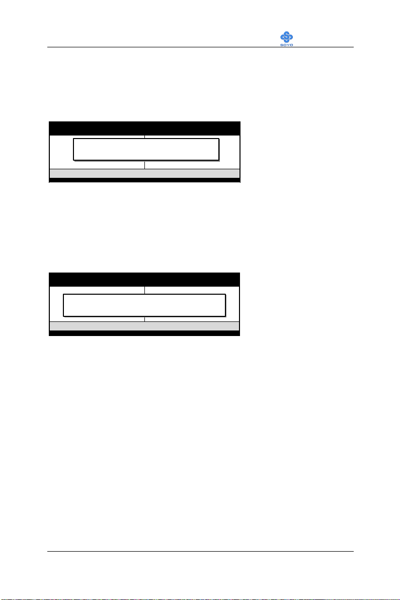
SAVE AND EXIT SETUP
Select the [SAVE & EXIT SETUP] option from the Main Menu to save
data to CMOS and exit the setup utility. This option saves all your changes
and causes the system to reboot.
ROM PCI/ISA BIOS
CMOS SETUP UTILITY
STANDARD CMOS SETUP
BIOS FEATURES SETUP
CHIPSET FEATURES SETUP
POWER MANAGEMENT SETUP
PNP/PCI CONFIGURATION
LOAD SETUP DEFAULTS
LOAD BIOS DEFAULTS
: Quit
: Save & Exit Setup
AWARD SOFTWARE, INC.
SAVE to CMOS and EXIT
Time, Date, Hard Disk Type…
INTEGRATED PERIPHERALS
SUPERVISOR PASSWORD
USER PASSWORD
IDE HDD AUTO DETECTION
SAVE & EXIT SETUP
EXIT WITHOUT SAVING
↑ ↓ → ←
: Select Item
: Change Color
Type [Y] to save the
changes and exit or [N]
to return to the Main
Menu and keep current
values.
EXIT WITHOUT SAVING
Selecting the [EXIT WITHOUT SAVING] option allows you to abandon
all data and exit setup, therefore ignoring all your changes.
ROM PCI/ISA BIOS
CMOS SETUP UTILITY
STANDARD CMOS SETUP
BIOS FEATURES SETUP
CHIPSET FEATURES SETUP
POWER MANAGEMENT SETUP
PNP/PCI CONFIGURATION
LOAD SETUP DEFAULTS
LOAD BIOS DEFAULTS
: Quit
: Save & Exit Setup
AWARD SOFTWARE, INC.
Quit Without Saving (Y/N)? _
Time, Date, Hard Disk Type…
INTEGRATED PERIPHERALS
SUPERVISOR PASSWORD
USER PASSWORD
IDE HDD AUTO DETECTION
SAVE & EXIT SETUP
EXIT WITHOUT SAVING
↑ ↓ → ←
: Select Item
: Change Color
Type [Y] to abandon
changes and exit or [N]
to return to the Main
Menu and keep current
values.
52
Page 57

BIOS Setup Utility SY-7VDA
3-1 SOYO COMBO SETUP
This Motherboard does not use any hardware jumpers to set the CPU
frequency. Instead, CPU settings are software configurable with the BIOS
[SOYO COMBO SETUP].
After the hardware installation is complete, turn the power switch on, then
press the <DEL> key during the system diagnostic checks to enter the
Award BIOS Setup program. The CMOS SETUP UTILITY will display on
screen. Then, select the [SOYO COMBO SETUP] option from the main
menu and press the <Enter> key.
CMOS Setup Utility – Copyright ( C ) 1984-2001 Award Software
SOYO COMBO Feature
Auto Detect DIMM/PCI Clk Enabled
Spread Spectrum Disabled
CPU Clock 66MHz
CPU Ratio X 3
CPU Vcore Select Default
Quick Power On Self Test Enabled
First Boot Device Floppy
Second Boot Device HDD-0
Third Boot Device LS120
Boot Other Device Enabled
áâà:Move Enter:Select +/-/PU/PD:Value F10:Save ESC:Exit F1:General Help
F5:Previous Values F6:Fail-Safe Defaults F7: Optimized Defaults
Menu Level 4
Item Help
The [SOYO COMBO SETUP] menu combines the main parameters that
you need to configure, all in one menu, for a quick setup in BIOS.
53
Page 58
BIOS Setup Utility SY-7VDA
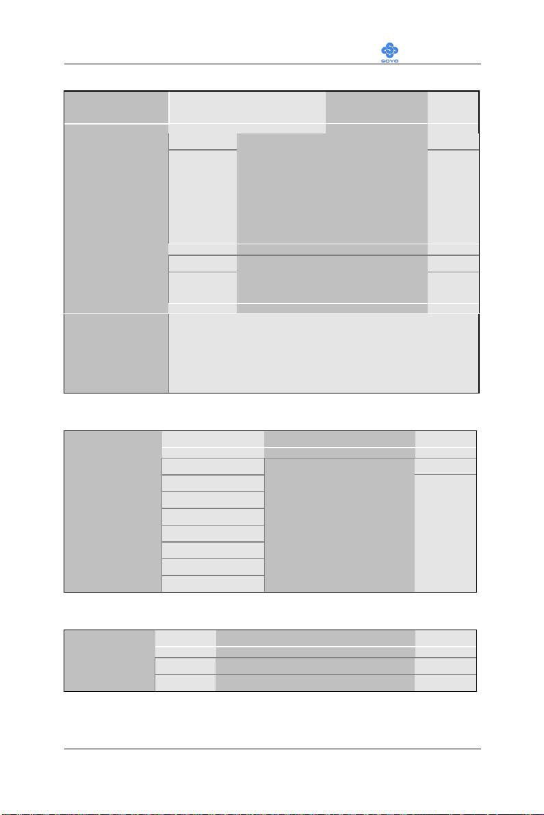
Quick CPU Frequency Setup
Quick CPU
Frequency Setup
Setting Description Note
Auto Detect
DIMM/PCI Clk
Spread
Spectrum
CPU Clock
Ratio
Disabled
Enabled
Disabled Default
Enabled
After you have selected the host clock, choose the right
multiplier for the CPU. Options are: [2, 2.5, 3., 3.5, 4, 4.5, 5,
5.5,6,6.5,7.0,7.5,8.0]. The CPU frequency is then defined as
[host clock freq.]x[multiplier], and should the working
frequency of your Pentium® III & Pentium® II processor.
CPU Vcore Select
Setting Description Note
CPU Vcore
Select
Default Default
+0.05V
+0.1V
+0.2V
+0.3V
+0.4V
-0.05V
-0.1V
When enabled, this item will auto
detect if the DIMM and PCI
socket have devices and will send
clock signal to DIMM and PCI
devices. When disabled, it will
send the clock signal to all
DIMM and PCI socket.
This item allows you to
enable/disable the spread
spectrum modulate.
This function adjust the
CPU voltage.
Default
Quick Power On Self Test
Setting Description Note
Quick Power
On Self Test
Disabled
Enabled Provides a fast POST at boot-up. Default
54
Page 59
BIOS Setup Utility SY-7VDA
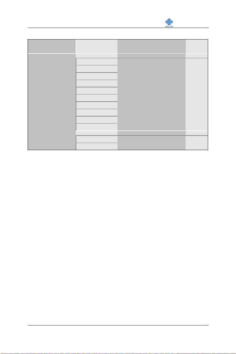
System Boot Control Settings
System Boot
Control Settings
Setting Description Note
First
/Second/Third
Boot Device
Boot Other
Device
Floppy
LS/ZIP
HDD-0
SCSI
CDROM
HDD-1
HDD-2
HDD-3
LAN
Disabled
Disabled
Enabled
Select Your Boot Device
Priority
Select Your Boot Device
Priority
Default
55
Page 60
BIOS Setup Utility SY-7VDA
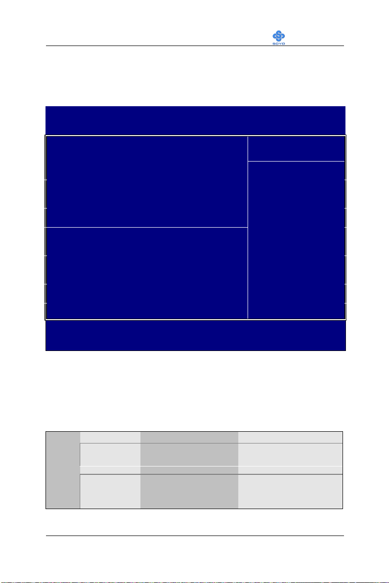
3-2 STANDARD CMOS SETUP
Select the [STANDARD CMOS SETUP] option from the Main Menu and
press [Enter] key.
CMOS Setup Utility – Copyright ( C ) 1984-2001 Award Software
Standard CMOS Features
Date (mm:dd:yy) Fri, Mar 9 2001
Time (hh:mm:ss) 16 : 40 : 51
4 IDE Primary Master Press Enter None
4 IDE Primary Slave Press Enter None
4 IDE Secondary Master Press Enter None
4 IDE Secondary Slave Press Enter None
Drive A 1.44M, 3.5 in.
Drive B None
Floppy 3 Mode Support Disabled
Video EGA/VGA
Halt On All Errors
Base Memory 640K
Extended Memory 130048K
Total Memory 131072K
áâà:Move Enter:Select +/-/PU/PD:Value F10:Save ESC:Exit F1:General Help
F5:Previous Values F6:Fail-Safe Defaults F7: Optimized Defaults
Menu Level 4
Item Help
This screen allows you to modify the basic CMOS settings.
After you have completed the changes, press [Esc] key to return to the
Main Menu.
Date & Time
Display Setting Please Note
Date
mm/dd/yyyy Type the current date You can also the
PUp/PDn keys to toggle
Time
hh:mm:ss Type the current time 24-hour clock format
3:15 PM is displayed as
15:15:00
56
Page 61
BIOS Setup Utility SY-7VDA
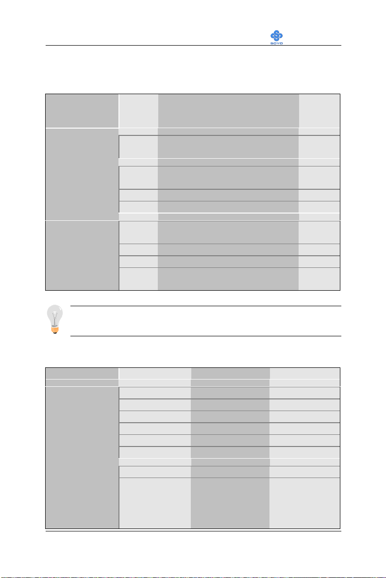
Hard Disks Type & Mode
Choose the type and mode for the hard disks that you have already
installed.
Primary
(Secondary)
Master & Slave
Setting Description Note
IDE HDD AutoDetection
IDE Primary
Slave
(User Type)
Press
Enter
Auto BIOS detects hard disk type
User User defines the type of hard disk.
To auto-detect the HDD’s size,
head… on this channel
automatically.
None
Access Mode
Auto BIOS detects hard disk mode
automatically.
Normal Normal IDE hard disk <528MB
LBA Enhanced IDE hard disk >528MB
Large Large IDE hard disk (for certain
hard disk)
Note: If you have any questions on your hard disk type or mode, ask
your hard disk provider or previous user for details.
Floppy Drives
Floppy Drives Setting Description Note
Drives A & B
360KB, 5.25 in.
1.2MB, 5.25 in.
720KB, 3.5 in.
1.44MB, 3.5 in. Default
2.88MB, 3.5 in.
None Not installed
Default
Default
Floppy 3-Mode
Support
Disabled Default
Drive A
Drive B
Both
Supports 3-mode
floppy diskette:
740KB/1.2MB/
1.44MB on selected
disk drive.
Special disk drive
commonly used in
Japan
57
Page 62
BIOS Setup Utility SY-7VDA
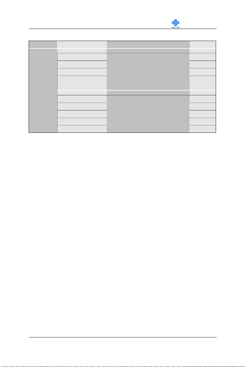
Others Optional
Setting Description Note
Video
Halt On
EGA/VGA Default
CGA 40
CGA 80
MONO
(Monochrome)
ALL Errors Default
No Errors
All, But Keyboard
All, But Diskette
All, But Disk/Key
Select the video mode.
When the BIOS detects system
errors, this function will stop the
system. Select which type of
error will cause the system halt.
58
Page 63

BIOS Setup Utility SY-7VDA
3-3 ADVANCED BIOS FEATURES
Select the [Advanced BIOS Features] option from the Main Menu and
press [Enter] key.
CMOS Setup Utility – Copyright ( C ) 1984-2001 Award Software
Advanced BIOS Features
Virus Warning Disabled
CPU Internal Cache Enabled
External Cache Enabled
CPU L2 Cache ECC Checking Enabled
Swap Floppy Drive Disabled
Boot Up Floppy Seek Enabled
Boot Up NumLock Status On
Gate A20 Option Fast
Typematic Rate Setting Disabled
x Typematic Rate (Chars/Sec) 6
x Typematic Delay (Msec) 250
Security Option Setup
OS Select For DRAM > 64MB Non-OS2
HDD S.M.A.R.T. Capability Disabled
Video BIOS Shadow Enabled
áâà:Move Enter:Select +/-/PU/PD:Value F10:Save ESC:Exit F1:General Help
F5:Previous Values F6:Fail-Safe Defaults F7: Optimized Defaults
Item Help
Menu Level 4
After you have completed the changes, press [Esc] key and follow the
instructions on your screen to save your settings or exit without saving.
Virus Warning
Setting Description Note
Virus
Warning
Disabled Default
Enabled
If set to enabled, the Paragon AntiVirus. Function will scan your boot
drive for boot virusses. If a boot
virus is detected, the BIOS will
display a warning message.
59
Page 64
BIOS Setup Utility SY-7VDA
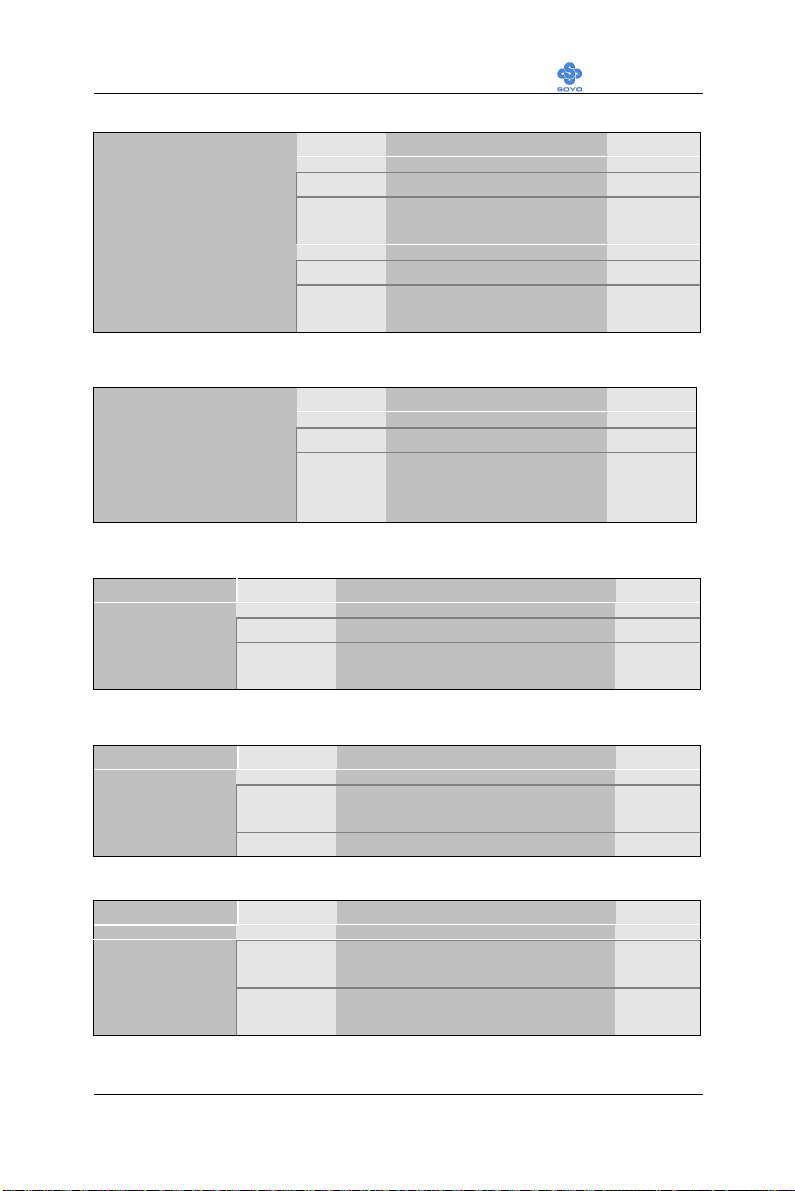
Cache Memory Options
Setting Description Note
CPU Internal Cache
External Cache
Disabled
Enabled Enables the CPU's internal
Disabled
Enabled Enables the external
L2 Cache Memory
Setting Description Note
CPU L2 Cache ECC
Checking
Disabled
Enabled This option activates the
Floppy Driver Settings
Setting Description Note
Swap Floppy
Drive
Disabled Default
Enabled Changes the sequence of A and B
Boot Up Floppy Seek
Setting Description Note
Default
cache.
Default
memory.
Default
CPU L2 cache ECC
checking function.
drives.
Boot Up Floppy
Seek
Disabled Seeks disk drives during boot up.
Disabling speeds boot up.
Enabled Default
Boot Up NumLock Status
Setting Description Note
Boot Up
NumLock
Status
On Puts numeric keypad in
NumLock mode at boot-up.
Off Puts numeric keypad in arrow key
mode at boot-up.
Default
60
Page 65
BIOS Setup Utility SY-7VDA
Gate A20 Options
Setting Description Note
Gate A20
Options
Normal Lets chipset control GateA20.
Fast A pin in the keyboard controller
Default
controls GateA20.
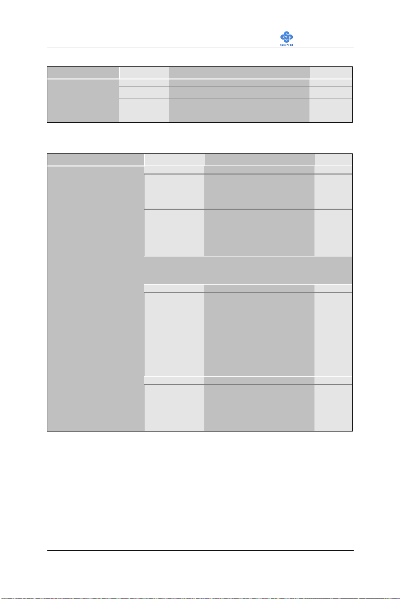
Typematic Settings
Typematic Settings Setting Description Note
Typematic
Rate Setting
Disabled Keystrokes repeat at a rate
determined by the
keyboard.
Enabled When enabled, the
typematic rate and
typematic delay can be
selected.
The following [Typematic Rate] and [Typematic Delay] fields are active
only if [Typematic Rate Setting] is set to [Enabled]
Typematic Rate
6 (Char/sec)
8 (Char/sec)
10 (Char/sec)
12 (Char/sec)
15 (Char/sec)
20 (Char/sec)
24 (Char/sec)
30 (Char/sec)
Choose the rate at which a
character is repeated when
holding down a key.
Default
Default
Typematic Delay
250 (msec)
500 (msec)
750 (msec)
1000 (msec)
Choose how long after
you press a key down the
character begins
repeating.
61
Default
Page 66

BIOS Setup Utility SY-7VDA
Security Option
Use this feature to prevent unauthorized system boot-up or use of BIOS
Setup. The following table describes the security settings.
Setting Description Note
Security Option
System Each time the system is booted,
the password prompt appears.
Setup If a password is set, the password
prompt only appears when you
attempt to enter the BIOS Setup
program.
Default
Other Control Options
Other Control
Options
Setting Description Note
OS Select for
DRAM>64MB
HDD S.M.A.R.T
Capability
Video BIOS
Shadow
OS2 When using an OS2 operating
system.
Non-OS2 When using another,
non-OS2 operating system.
Disabled Default
Enabled
Disabled
Enabled The BIOS is shadowed in a 16K
segment if it is enabled and if it
has BIOS present.
These 16 segments can be
shadowed from ROM to RAM.
BIOS shadow copies BIOS code
from slower ROM to faster RAM.
BIOS can then execute from
RAM.
Default
Default
62
Page 67

BIOS Setup Utility SY-7VDA
3-4 ADVANCED CHIPSET FEATURES
Select the [Advanced Chipset Features] option from the Main Menu and
press [Enter] key.
Caution: Change these settings only if you are already familiar
with the Chipset.
The [Advanced Chipset Features] option changes the values of the chipset
registers. These registers control the system options in the computer.
CMOS Setup Utility – Copyright ( C ) 1984-2001 Award Software
Advanced Chipset Features
4 DRAM Clock/Driver Control Press Enter
4 AGP & P2P Bridge Control Press Enter
4 CPU & PCI Bus Control Press Enter
Memory Hole Disabled
System BIOS Cacheable Disabled
Video RAM Cacheable Disabled
Memory Parity/ECC Check Disabled
áâà:Move Enter:Select +/-/PU/PD:Value F10:Save ESC:Exit F1:General Help
F5:Previous Values F6:Fail-Safe Defaults F7: Optimized Defaults
Menu Level 4
Item Help
After you have completed the changes, press [Esc] and follow the
instructions on your screen to save your settings or exit without saving.
The following table describes each field in the Advanced Chipset Features
Menu and how to configure each parameter.
63
Page 68

BIOS Setup Utility SY-7VDA
CHIPSET FEATURES SETUP
CHIPSET
FEATURES
Setting Description Note
Memory Hole
System BIOS
Cacheable
Video RAM
Cacheable
Memory
Parity/ECC
Check
Disabled Default
Enabled Some interface cards will map
their ROM address to this area. If
this occurs, select [Enabled] in
this field.
Disabled
Enabled The ROM area F0000H-FFFFFH
is cacheable.
Disabled Default
Enabled
Disabled Default
Enabled This item enabled to detect the
When synchronous DRAM is
installed, the number of clock
cycles of CAS latency depends on
the DRAM timing. Do not reset
this field from the default value
specified by the system designer
memory parity and Error
Checking & Correcting.
Default
64
Page 69

BIOS Setup Utility SY-7VDA
3-4.1 DRAM Clock/Drive Control
Caution: Change these settings only if you are already familiar
with the Chipset.
The [DRAM Clock/Drive Control] option changes the values of the chipset
registers. These registers control the system options in the computer.
CMOS Setup Utility – Copyright ( C ) 1984-2001 Award Software
DRAM Clock/Drive Control
Current FSB Frequence 66MHz
DRAM Clock By SPD
DRAM Timing By SPD
x SDRAM Cycle Length 2.5
x Bank Interleave Disabled
DRAM Command Rate 2T Command
áâà:Move Enter:Select +/-/PU/PD:Value F10:Save ESC:Exit F1:General Help
F5:Previous Values F6:Fail-Safe Defaults F7: Optimized Defaults
Menu Level 4
Item Help
After you have completed the changes, press [Esc] and follow the
instructions on your screen to save your settings or exit without saving.
65
Page 70
BIOS Setup Utility SY-7VDA
DRAM Clock/Drive Control
Setting Description Note
DRAM Clock
/Driver Control
DRAM Timing
SDRAM Cycle
Length
Bank Interleave
DRAM Command
Rate
By SPD Default
HCLK-33M
HCLK+33M
By SPD Default
Manual
2.5 Default
2
This item allows you to
control the DRAM speed.
If enable the DRAM will auto
detect the DRAM timing.
When synchronous DRAM is
installed, the number of clock
cycles of CAS latency
depends on the DRAM
timing. Do not reset this field
from the default value
specified by the system
designer.
Disabled
Increase DRAM performance.
2 Bank Default
4 Bank
2T Command Default
Increase DRAM performance.
1T Command
66
Page 71

BIOS Setup Utility SY-7VDA
3-4.2 AGP & P2P Bridge Control
Caution: Change these settings only if you are already familiar
with the Chipset.
The [AGP & P2P Bridge Control] option changes the values of the chipset
registers. These registers control the system options in the computer.
CMOS Setup Utility – Copyright ( C ) 1984-2001 Award Software
AGP & P2P Bridge Control
AGP Aperture Size 64M
AGP Mode 4X
AGP Driving Control Auto
x AGP Driving Value DA
AGP Fast Write Disabled
AGP Master 1 WS Write Disabled
AGP Master 1 WS Read Disabled
áâà:Move
Enter:Select +/-/PU/PD:Value F10:Save ESC:Exit F1:General Help
F5:Previous Values F6:Fail-Safe Defaults F7: Optimized Defaults
Menu Level 4
Item Help
After you have completed the changes, press [Esc] and follow the
instructions on your screen to save your settings or exit without saving.
67
Page 72

BIOS Setup Utility SY-7VDA
3-4.3 AGP & P2P Bridge Control
Setting Description Note
AGP Aperture
Size
AGP Mode
AGP Driving
Control
AGP Driving
Value
AGP Fast
Write
64M Default
4M, 8M,
16M, 32M,
128M,
256M.
1X
2X
4X Default
Auto Default
Manual
Min=0000
~
Max=00FF
Disabled Default
Enabled
Select the size of Accelerated
Graphics Port (AGP) aperture. The
aperture is a portion of the PCI
memory address range dedicated for
graphics memory address space.
Host cycles that hit the aperture
range are forwarded to the AGP
without any translation.
This item allows you to enable /
disable the AGP-4X Mode.
This item allows you to adjust the
AGP driving force. Choose Manual
to key in a AGP Driving Value in
the next selection. This field is
recommended to set in Auto for
avoiding any error in your system.
This item allows you to adjust the
AGP driving force.
The VIA chipset will use fast write
to AGP if this item is enabled. Not
all AGP cards support fast write.
AGP Master 1
WS Write
AGP Master 1
WS Read
Disabled Default
Enabled When Enabled, writes to the
AGP(Accelerated Graphics Port) are
executed with one wait states.
Disabled Default
Enabled When Enabled, read to the AGP
(Accelerated Graphics Port) are
executed with one wait states.
68
Page 73

BIOS Setup Utility SY-7VDA
3-4.4 CPU & PCI Bus Control
Caution: Change these settings only if you are already familiar
with the Chipset.
The [CPU & PCI Bus Control] option changes the values of the chipset
registers. These registers control the system options in the computer.
CMOS Setup Utility – Copyright ( C ) 1984-2001 Award Software
CPU & PCI Bus Control
CPU to Write Buffer Enabled
PCI Master 0 WS Write Enabled
PCI Delay Transaction Disabled
áâà:Move
Enter:Select +/-/PU/PD:Value F10:Save ESC:Exit F1:General Help
F5:Previous Values F6:Fail-Safe Defaults F7: Optimized Defaults
Menu Level 4
Item Help
After you have completed the changes, press [Esc] and follow the
instructions on your screen to save your settings or exit without saving.
69
Page 74

BIOS Setup Utility SY-7VDA
CPU & PCI Bus Control
Setting Description Note
CPU to PCI
Write Buffer
Disabled
Enabled
When this field is Enabled, writes
from the CPU to the PCI bus are
buffered, to compensate for the
speed differences between the CPU
and the PCI bus. When Disabled,
the writes are not buffered and the
CPU must wait until the write is
complete before starting another
write cycle.
Default
PCI Master 0
WS Write
PCI Delay
Transaction
Disabled
Enabled When Enabled, writes to the PCI
bus are executed with zero wait
states.
Disabled Default
Enabled
The chipset has an embedded 32-bit
posted write buffer to support delay
transactions cycles. Select Enabled
to support compliance with PCI
specification version 2.1.
Default
70
Page 75
BIOS Setup Utility SY-7VDA
3-5 INTEGRATED PERIPHERALS
Select the [Integrated Peripherals] option from the Main Menu and press
[Enter] key.
Caution: Change these settings only if you are already familiar
with the Chipset.
The [INTEGRATED PERIPHERALS] option changes the values of the
chipset registers. These registers control the system options in the computer.
The following screen shows setup default settings.
CMOS Setup Utility – Copyright ( C ) 1984-2001 Award Software
Integrated Peripherals
4 VIA OnChip IDE Device Press Enter
4 VIA OnChip PCI Device Press Enter
4 VIA SuperIO Device Press Enter
Init Display First PCI Slot
OnChip USB Controller All Enabled
USB Keyboard Support Disabled
IDE HDD Block Mode Enabled
PWRON After PWR-Fail Off
Menu Level 4
Item Help
áâà:Move
Enter:Select +/-/PU/PD:Value F10:Save ESC:Exit F1:General Help
F5:Previous Values F6:Fail-Safe Defaults F7: Optimized Defaults
After you have completed the changes, press [Esc] and follow the
instructions on your screen to save your settings or exit without saving.
INTEGRATED PERIPHERALS
Setting Description Note
Init Display First
PCI Slot Default
AGP
Choose which card – AGP
Display card or PCI VGA
card – to initialize first.
71
Page 76
BIOS Setup Utility SY-7VDA
INTEGRATED PERIPHERALS
Setting Description Note
OnChip USB
Controller
USB Keyboard
Support
IDE HDD Block
Mode
PWRON After
PWR-Fail
All Disabled
All Enabled Default
1&2 USB Port
2&3 USB Port
3&1 USB Port
1 USB Port
2 USB Port
3 USB Port
Disabled Default
Enabled
Disabled
Enabled
Off The system will switch on
On The system will remain off
Former-Sts The system will return to
This should be enabled if
your system has a USB
installed on the system
board and you want to use
it. Even when so equipped,
if you add a higher
performance controller, you
will need to disable this
feature.
Port 1 means USB1&2
Port 2 means USB3&4
Port 3 means USB5&6
Select Enabled if your
system contains a Universal
Serial Bus (USB) controller
and you have a USB
keyboard.
Invokes multi-sector
transfer instead of one
sector per transfer. Not all
HDDs support this
function.
when power comes back
after a power failure.
when power comes back
after a power failure.
the state it was in before the
power failure when power
returns. (i.e: If the system
was on, it will switch on
again, if it was off, it will
remain off)
Default
Default
72
Page 77

BIOS Setup Utility SY-7VDA
3-5.1 VIA OnChip IDE Device
Caution: Change these settings only if you are already familiar
with the Chipset.
The [VIA OnChip IDE Device] option changes the values of the chipset
registers. These registers control the system options in the computer.
The following screen shows setup default settings.
CMOS Setup Utility – Copyright ( C ) 1984-2001 Award Software
VIA OnChip IDE Device
OnChip IDE Channel0 Enabled
OnChip IDE Channel1 Enabled
IDE Prefetch Mode Enabled
Primary Master PIO Auto
Primary Slave PIO Auto
Secondary Master PIO Auto
Secondary Slave PIO Auto
Primary Master UDMA Auto
Primary Slave UDMA Auto
Secondary Master UDMA Auto
Secondary Slave UDMA Auto
áâà:Move Enter:Select +/-/PU/PD:Value F10:Save ESC:Exit F1:General Help
F5:Previous Values F6:Fail-Safe Defaults F7: Optimized Defaults
Menu Level 4
Item Help
After you have completed the changes, press [Esc] and follow the
instructions on your screen to save your settings or exit without saving.
73
Page 78

BIOS Setup Utility SY-7VDA
VIA OnChip IDE Device
Setting Description Note
On-Chip PCI IDE
Ø Primary
Ø Secondary
IDE
Ø Primary Master PIO
Ø Primary Slave PIO
Ø Secondary Master PIO
Ø Secondary Slave PIO
IDE
Ø Primary Master UDMA
Ø Primary Slave UDMA
Ø Secondary Master UDMA
Ø Secondary Slave UDMA
Disabled Turn off the on-board
IDE
Enabled Use the on-board IDE Default
mode 0-4 0 is the slowest speed
4 is the fastest speed
Auto For better performance
Default
and stability, we suggest
you use the Auto setting
to set the HDD control
timing.
Disabled
Auto Select Auto to enable
Default
Ultra DMA Mode
support.
74
Page 79
BIOS Setup Utility SY-7VDA
3-5.2 VIA OnChip PCI Device
Caution: Change these settings only if you are already familiar
with the Chipset.
The [VIA OnChip PCI Device] option changes the values of the chipset
registers. These registers control the system options in the computer.
The following screen shows setup default settings.
CMOS Setup Utility – Copyright ( C ) 1984-2001 Award Software
Integrated Peripherals
VIA-3058 AC97 Audio Auto
Menu Level 4
áâà:Move Enter:Select +/-/PU/PD:Value F10:Save ESC:Exit F1:General Help
F5:Previous Values F6:Fail-Safe Defaults F7: Optimized Defaults
Item Help
After you have completed the changes, press [Esc] and follow the
instructions on your screen to save your settings or exit without saving.
VIA OnChip PCI Device
Setting Description Note
VIA-3058 AC97 Audio
Auto Default
Disabled
This item allows you to
control the onboard AC
97 audio.
75
Page 80
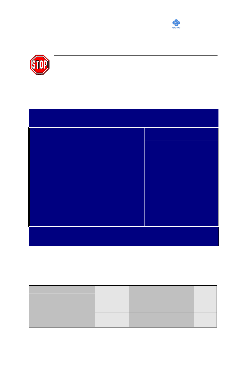
BIOS Setup Utility SY-7VDA
3-5.3 VIA SuperIO Device
Caution: Change these settings only if you are already familiar
with the Chipset.
The [VIA SuperIO Device] option changes the values of the chipset
registers. These registers control the system options in the computer.
The following screen shows setup default settings.
CMOS Setup Utility – Copyright ( C ) 1984-2001 Award Software
VIA SuperIO Device
Onboard FDD Controller Enabled
Onboard Serial Port 1 3F8/IRQ4
Onboard Serial Port 2 2F8/IRQ3
UART Mode Select Normal
x RxD , TxD Active Hi , Lo
x IR Transmission Delay Enabled
x UR2 Duplex Mode Half
x Use IR Pins IR-Rx2Tx2
Onboard Parallel Port 378/IRQ7
Parallel Port Mode SPP
x ECP Mode Select EPP1.7
x ECP Mode Use DMA 3
Game Port Address 201
Midi Port Address 330
Midi Port IRQ 10
Menu Level 4
Item Help
áâà:Move Enter:Select +/-/PU/PD:Value F10:Save ESC:Exit F1:General Help
F5:Previous Values F6:Fail-Safe Defaults F7: Optimized Defaults
After you have completed the changes, press [Esc] and follow the
instructions on your screen to save your settings or exit without saving.
VIA SuperIO Device
Setting Description Note
Onboard FDD
controller
Disabled Turn off the on-board
floppy controller
Enabled Use the on-board floppy
controller
76
Default
Page 81
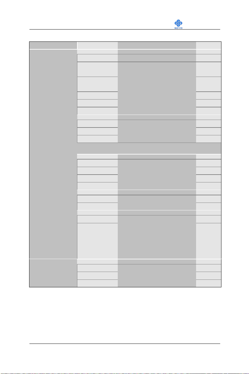
BIOS Setup Utility SY-7VDA
VIA SuperIO Device
Setting Description Note
Onboard
Serial Port 1 /
Serial Port 2
UART 2 Mode
If [UART Mode Select] is set to [IrDA]/[ASKIR]
RxD, TxD Active
IR Transmission
Delay
UR2 Function
Duplex
Disabled
3F8/IRQ4 Default
2F8/IRQ3 Default
3E8/IRQ4
2E8/IRQ3
Auto
IrDA
ASKIR
Normal
Hi, Hi
Hi, Lo Default
Lo, Hi
Lo, Lo
Disabled
Enabled
Half Default
Full
Choose serial port 1 & 2's I/O
address.
Do not set port 1 & 2 to the
same address except for
Disabled or Auto.
The second serial port offers
these InfraRed interface
modes.
This item allows you to
determine the active RxD,
TxD.
Some IR devices need this
item enabled.
Choose [Half] or [Duplex] to
set UR2 in half duplex mode
or full duplex mode
respectively. Refer to your IR
device specifications to select
the suitable mode.
(port 1)
(port 2)
Defanlt
Default
Use IR Pins
RxD2
TxD2
IR-Rx2Tx2 Default
77
Page 82
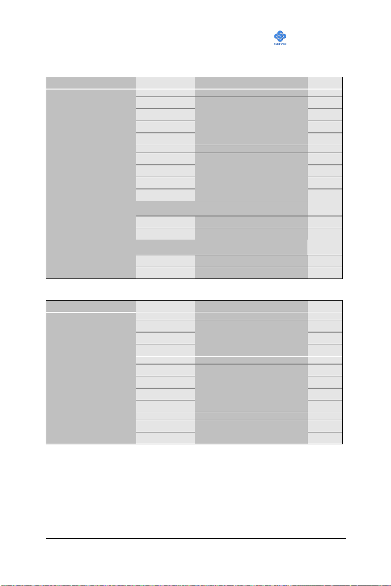
BIOS Setup Utility SY-7VDA
If [Parallel Port Mode] is set to [ECP] mode
If [Parallel Port Mode] is set to [EPP] mode
VIA SuperIO Device
Setting Description Note
Onboard Parallel
Port
Disabled
378/IRQ7 Default
Choose the printer I/O
address.
278/IRQ5
3BC/IRQ7
Parallel Port Mode
SPP Default
EPP
ECP
The mode depends on your
external device that
connects to this port.
ECP+EPP
ECP Mode use
DMA
Parallel Port EPP
TYPE
3 Choose DMA3 Default
1 Choose DMA1
EPP 1.9 Select EPP port type 1.9
EPP 1.7 Select EPP port type 1.7 Default
This field controls the onboard legacy audio.
Setting Description Note
Game Port (200207H)
Disabled
201 Default
Set this item to enabled to
make use of the game port.
209
Midi Port Address
Disabled
330 Default
Select the I/O address for
your MIDI functionality.
300
290
Midi Port IRQ
5
10
Select the IRQ for your
MIDI port.
78
Default
Page 83
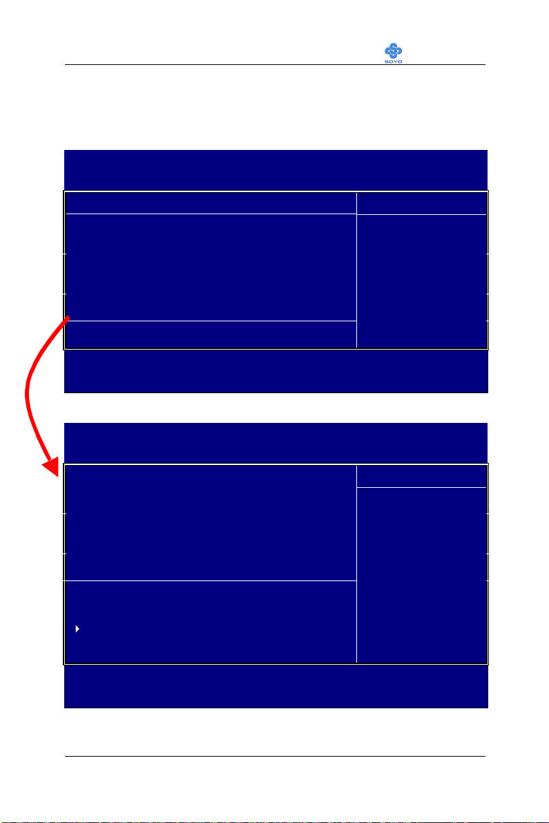
BIOS Setup Utility SY-7VDA
3-6 POWER MANAGEMENT SETUP
The [POWER MANAGEMENT SETUP] sets the system's power saving
functions.
CMOS Setup Utility – Copyright ( C ) 1984-2001 Award Software
Power Management Setup
4 ACPI Suspend Type S1 (POS) Item Help
Power Management Option User Define
HDD Power Down Disable
Suspend Mode Disable
Video Off Option Suspend -> Off
Video Off Method V/H SYNC+Blank
MODE Use IRQ 3
Soft-Off by PWRBTN Instant-Off
4 IRQ/Event Activity Detect Press Enter
áâà:Move Enter:Select +/-/PU/PD:Value F10:Save ESC:Exit F1:General Help
F5:Previous Values F6:Fail-Safe Defaults F7: Optimized Defaults
CMOS Setup Utility – Copyright ( C ) 1984-2001 Award Software
IRQ/Event Activity Detect
Menu Level 4
PS2KB Wakeup from S3/S4/S5 Disabled Item Help
USB Resume from S3/S4/S5 Disabled
VGA OFF
LPT & COM LPT/COM
HDD & FDD ON
PCI Master OFF
PowerOn by PCI Card Disabled
Modem Ring Resume Disabled
RTC Alarm Resume Disabled
x Date (of Month) 0
x Resume Time (hh:mm:ss)
IRQs Activity Monitoring Press Enter
áâà:Move Enter:Select +/-/PU/PD:Value F10:Save ESC:Exit F1:General Help
F5:Previous Values F6:Fail-Safe Defaults F7: Optimized Defaults
0¡G0¡G0
Menu Level 4
After you have completed the Power Management Setup, press [Esc] to
return to the Main Menu.
79
Page 84

BIOS Setup Utility SY-7VDA
Power Management Controls
Setting Description Note
ACPI Suspend
Type
Power
Management
Option
HDD Power
Down
Suspend Mode
Video Off
Option
S1(POS) Default
S3(STR)
User Define Default
Min Saving 15 Min
Max Saving
Disabled Default
1Min, 2Min,
3Min, 4Min,
5Min, 6Min,
7Min, 8Min,
9Min, 10Min,
11Min, 12Min,
13Min, 14Min,
15Min
Disabled Default
1Min, 2Min,
4Min, 6Min,
8Min, 10Min,
20Min, 30Min,
40Min, 1Hour,
Suspend --> Off Default
Always On
All Modes -->
Off
The system will enter the S1
state during suspend. (Low
latency wake up)
Lets you define the system
power down times.
1 Min
Lets you define the system
power down times.
Lets you define the system
power down times.
When enabled, this feature
allows the VGA adapter to
operate in a power saving
mode.
Video Off
Method
V/H Sync+Blank Default
Blank screen
DPMS Support
Selects the method by which
the monitor is blanked.
80
Page 85
BIOS Setup Utility SY-7VDA
Power Management Controls (Continued)
Setting Description Note
MODEM Use
IRQ
Soft-Off by
PWR-BTTN
IRQ/Event
Activity
3 Default
3-11, NA
Instant-off Default
Delay 4 Sec. Turns off the system power 4
Press Enter Select items that will wake up
IRQ/Event Activity Detect
Setting Description Note
PS2KB
Wakeup from
S3/S4/S5
USB Resume
from S3/S4/S5
LPT & COM
Disabled Default
Ctrl+F1~F12
Power
Wake
Any Key
Disabled Default
Enabled
LPT/COM
NONE,
LPT,
COM
Assigns an IRQ# to the modem
device.
seconds after pushing the power
button.
your system when in one of
sleep modes. Press enter to go
the select item page.
You can set the PS2KB Hotkey
to Wakeup system from
S3/S4/S5
You can set the USB to Resume
system from S3/S4/S5
When On of LPT & COM, any
activity from one of the listed
system peripheral devices or
IRQs wakes up the system.
Default
HDD & FDD
PCI Master
OFF Default
ON
OFF
ON
When On of HDD & FDD, any
activity from one of the listed
system peripheral devices wakes
up the system.
When On of PCI Master, any
activity from one of the listed
system peripheral devices wakes
up the system
81
Default
Page 86

BIOS Setup Utility SY-7VDA
IRQ/Event Activity Detect
Setting Description Note
PowerOn by
PCI Card
Modem Ring
Resume
RTC Alarm
Resume
Disabled Default
Enabled
Disabled Default
Enabled
Disabled The system ignores the alarm. Default
Enabled Set alarm to power on the
If enabled any PCI interrupt will
wake up the system.
An input signal on the serial
Ring Indicator (RI) line (in other
words, an incoming call on the
modem) awakens the system
from a soft off state.
system by the date (1-31) or
time (hh:mm:ss). If the date is
set to [0], the system will selfpower on by alarm everyday at
the set time.
82
Page 87

BIOS Setup Utility SY-7VDA
3-6.1 IRQs Activity Monitoring
This option sets the IRQs Activity Monitoring.
CMOS Setup Utility – Copyright ( C ) 1984-2001 Award Software
IRQs Activity Monitoring
Primary INTR NO
IRQ3 (COM 2) Enabled
IRQ4 (COM 1) Enabled
IRQ5 (LPT 2) Enabled
IRQ6 (Floppy Disk) Enabled
IRQ7 (LPT 1) Enabled
IRQ8 (RTC Alarm) Disabled
IRQ9 (IRQ2 Redir) Disabled
IRQ10 (Reserved) Disabled
IRQ11 (Reserved) Disabled
IRQ12 (PS/2 Mouse) Enabled
IRQ13 (Coprocessor) Enabled
IRQ14 (Hard Disk) Enabled
IRQ15 (Reserved) Disabled
áâà:Move Enter:Select +/-/PU/PD:Value F10:Save ESC:Exit F1:General Help
F5:Previous Values F6:Fail-Safe Defaults F7: Optimized Defaults
Item Help
Menu Level 4
After you have completed the changes, press [Esc] and follow the
instructions on your screen to save your settings or exit without saving.
83
Page 88

BIOS Setup Utility SY-7VDA
IRQs Activity Monitoring
Wake Up
Events
Setting Description Note
Primary INTR
IRQs Activity
Monitoring
(Press Enter)
ON Default
OFF
Primary IRQ3(COM2), IRQ4(COM1),
Secondary IRQ9(IRQ2 Redir),
Disabled IRQ8 (RTC Alarm), IRQ15
When set to On, any event occurring
at will awaken a system which has
been powered down.
IRQ5(LPT2), IRQ6(Floppy Disk),
IRQ7(LPT1), IRQ12(PS/2 mouse),
IRQ13(Coprocessor),
IRQ14(HardDsik)
IRQ10( Reserved),
IRQ11(Reserved)
(Reserved)
84
Page 89

BIOS Setup Utility SY-7VDA
3-7 PNP/PCI CONFIGURATIONS
This option sets the Motherboard’s PCI Slots.
CMOS Setup Utility – Copyright ( C ) 1984-2001 Award Software
PnP/PCI Configurations
PnP OS Installed NO
Reset Configuration Data Disabled
Resources Controlled By Auto (ESCD)
x IRQ Resources Press Enter
PCI/VGA Palette Snoop Disabled
Assign IRQ For VGA Enabled
Assign IRQ For USB Enabled
áâà:Move Enter:Select +/-/PU/PD:Value F10:Save ESC:Exit F1:General Help
F5:Previous Values F6:Fail-Safe Defaults F7: Optimized Defaults
Item Help
Menu Level 4
Select Yes if you are
using a Plug and Play
capable operating system
Select No if you need the
BIOS to configure nonboot devices
Note: Starred (*) items will disappear when the [Resources Controlled
By] option is set to [Auto].
After you have completed the PCI Slot Configuration, press [Esc] and
follow the instructions on your screen to save your settings or exit without
saving.
85
Page 90
BIOS Setup Utility SY-7VDA
PNP/PCI Configuration Controls
PNP/PCI
Controls
Setting Description Note
PnP OS
Installed
Yes Set this field to [Yes] if you
are running Windows 95,
which is PnP compatible.
Reset
Configuration
Data
No If the OS you are running
does not support PnP
configuration.
Disabled Retain PnP configuration
data in BIOS.
Enabled Reset PnP configuration data
Default
(If there is any
doubt, set this
field to [No])
Default
in BIOS.
Resources
Controlled By
Manual BIOS does not manage PCI/ISA PnP
card IRQ assignment.
Requires to assign IRQ-# and DMA-# to PCI or
ISA PnP manually.
IRQ-3,4,5,7,9,10,11,12,14,15 assigned to: _
DMA-0,1,3,5,6,7 assigned to: _
Auto
(ESCD)
The Plug-and-Play BIOS
auto manages PCI/ISA PnP
Recommended
card IRQ assignment
automatically.
If [Resources Controlled By] is set to [Manual]
IRQ-# and
DMA-#
assigned to:
PCI/ISA PnP Choose IRQ-# and
DMA-# assigned to
PCI/ISA PnP card.
Legacy ISA Choose IRQ-# and
DMA-# assigned to
Legacy ISA card.
Under this item the user can assign an IRQ to a PCI slot. However, there under
some conditions the IRQ will not be assigned as selected under this item:
1. IRQs 0, 1, 2, 6, 8, 13 can NOT be assigned, because they are fixed.
2. IRQs 5, 9, 10, 11 are available
3. IRQs 3,4,7,12,14 and 15 will only be assigned if they are free. See the table
below on how to free them:
IRQ-3,4,5,7,9,10,
11,12,14,15
DMA-0,1,3,5,6,7
IRQ-3,4,5,7,9,10,
11,12,14,15
DMA-0,1,3,5,6,7
86
Page 91
BIOS Setup Utility SY-7VDA
PNP/PCI Configuration Setup (Continued)
PNP/PCI
Setup
Interrupt
Line
IRQ 15 IRQ 15: PCI / ISA PnP On-Chip Secondary PCI IDE: disabled
IRQ 14 IRQ 14: PCI / ISA PnP On-Chip Primary PCI IDE: disabled
IRQ 12 IRQ 12: PCI / ISA PnP
IRQ 7 IRQ 7: PCI / ISA PnP Onboard parallel port: disabled
IRQ 4 IRQ 4: PCI / ISA PnP Onboard Serial port 1: disabled
IRQ 3 IRQ 3: PCI / ISA PnP Onboard Serial port 2: disabled
4. Your OS may reassign another interrupt to a PCI slot after BIOS passes control
to the OS, especially if you use Windows 95, 98 or NT.
Setting Description Note
How to set the BIOS to release the IRQ to the PnP Interrupt pool:
PnP / PCI configuration Integrated Peripherals
Interrupt 12 will be released by the PnP
BIOS automatically if the PS/2 Mouse Port
is not used.
Assign IRQ
For
VGA/USB
Disabled BIOS will assign IRQ for
VGA/USB port.
Enabled BIOS won’t assign IRQ for
Default
VGA/USB port.
5. Your OS may reassign another interrupt to a PCI slot after BIOS passes control
to the OS, especially if you use Windows 95, 98 or NT.
Auto DefaultINT Pin
1/2/3/4
Set to Auto the BIOS will
using IRQs Automatically.
Assignment
MULTI I/O ADDRESSES
Default settings for multi-I/O addresses are as follows:
Port I/O Address IRQ Status
LPT1
COM1
COM2
Warning: If a default I/O address conflicts with other I/O cards
such as sound card, you must change one of the I/O addresses to
remedy to this address conflict. (I/O addresses can be adjusted from
the BIOS Setup Utility)
378H 7 ECP/EPP
3F8H 4
2F8H 3
87
Page 92

BIOS Setup Utility SY-7VDA
3-8 PC HEALTH STATUS
This option sets the Motherboard's PC Health Status.
CMOS Setup Utility – Copyright ( C ) 1984-2001 Award Software
PC Health Status
CPU Warning Temp. Disabled
Current SYS Temp. 33 º C / 191 º F
Current CPU Temp. 33 º C / 191 º F
Current CPUFAN Speed 5192 RPM
Current CHAFAN Speed 0 RPM
Vcore 1.98 V
3.3 V 3.36 V
+ 5 V 4.97 V
- 12 V 12.03 V
+12 V -12.19 V
- 5 V - 4.99 V
VBAT (V) 3.16V
5VSB (V) 5.46V
Shutdown Twmperatuer Disabled
áâà:Move
Enter:Select +/-/PU/PD:Value F10:Save ESC:Exit F1:General Help
F5:Previous Values F6:Fail-Safe Defaults F7: Optimized Defaults
Item Help
Menu Level 4
Note: Starred (*) items will disappear when the [Resources Controlled
By] option is set to [Auto].
88
Page 93
BIOS Setup Utility SY-7VDA
CPU Device Monitoring
CPU Device
Monitoring
Setting Description Note
CPU Warning
Temperature
Current CPU
Temp.
Current System
Temp.
Current
CPUFAN/
CHAFAN Speed
Vcore 3.3V, +5V,
+12V, -12V, -5V,
VBAT(V),
5VSB(V)
Shutdown
Temperature
Disabled Default
50°C/122°F
53°C/127°F
56°C/132°F
60°C/140°F
63°C/145°F
66°C/150°F
70°C/158°F
°C/°F
°C/°F
RPM
V
Disabled Default
60°C/140°F,
65°C/149°F,
70°C/158°F,
Set CPU temperature from 50°C
to 70°C. The CPU will slow
down when CPU temperature
goes beyond the preset value.
The CPU will continue to run
slow until the temperature
returns back within the safe
range.
Show the current status of CPU
temperature.
Show the current status of the
system temperature.
Show the current status of CPU
Fan
Show the current voltage status.
This item allows you to set up
the CPU shutdown Temperature.
This item only effective under
Windows 98 ACPI mode.
89
Page 94
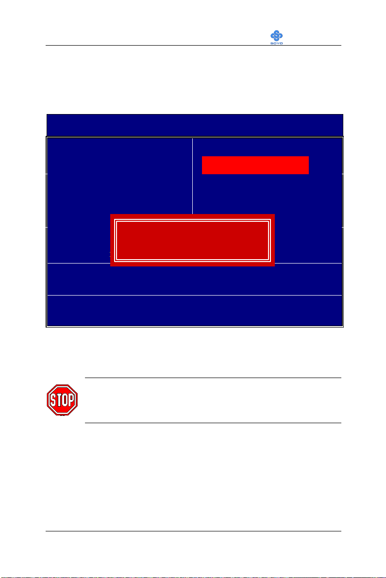
BIOS Setup Utility SY-7VDA
3-9 LOAD FAIL-SAFE DEFAULTS
Select the [Load Fail-Safe Defaults] option from the Main Menu to load
the system values you have previously saved. This option is recommended
if you need to reset the system setup and to retrieve the old values.
CMOS Setup Utility – Copyright ( C ) 1984-2001 Award Software
4SOYO COMBO Feature 4PC Health Status
4Standard CMOS Features Load Fail - Safe Defaults
4Advanced BIOS Features Load Optimized Defaults
4Advanced Chipset Features Set Supervisor Password
4Integrated Peripherals Set User Password
4Power Management Setup Save & Exit Setup
4PnP/PCI Configurations Exit Without Saving
Esc : Quit áâàß : Select Item
F10 : Save & Exit Setup
Load Fail - Safe Defaults (Y/N)? Y
Change CPU’s Clock & Voltage
Type [Y] to use the Setup Defaults followed by [Enter] or otherwise [N] to
return to the Main Menu and keep current values.
Warning: If you run into any problem after changing the BIOS
configuration, please load the Fail-Safe Defaults for stable
performance.
90
Page 95
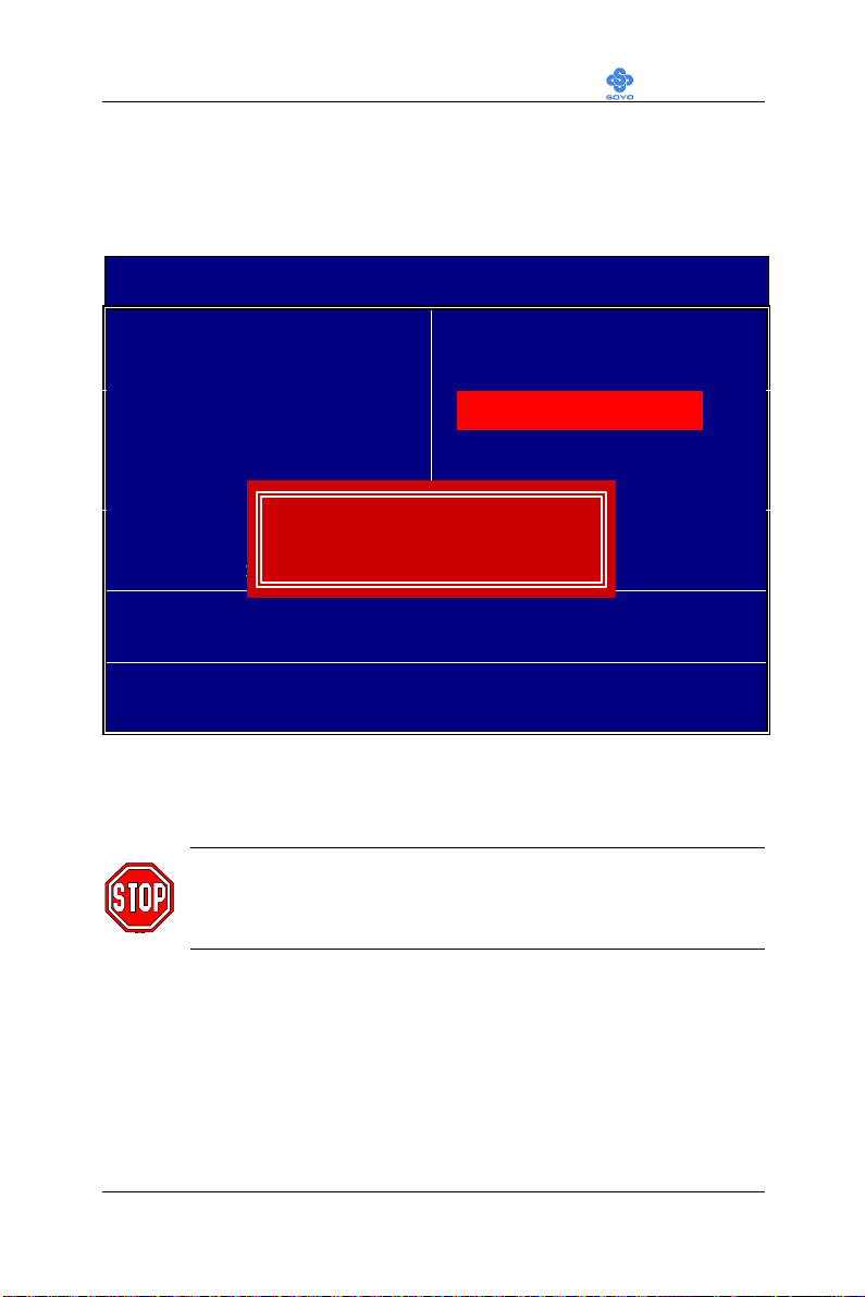
BIOS Setup Utility SY-7VDA
3-10 LOAD OPTIMIZED DEFAULTS
Select the [Load Optimized Defaults] option from the Main Menu to load
the system values you have previously saved. This option is recommended
if you need to reset the system setup and to retrieve the old values.
CMOS Setup Utility – Copyright ( C ) 1984-2001 Award Software
4SOYO COMBO Feature 4PC Health Status
4Standard CMOS Features Load Fail - Safe Defaults
4Advanced BIOS Features Load Optimized Defaults
4Advanced Chipset Features Set Supervisor Password
4Integrated Peripherals Set User Password
4Power Management Setup Save & Exit Setup
4PnP/PCI Configurations Exit Without Saving
Esc : Quit áâàß : Select Item
F10 : Save & Exit Setup
Load Optimized Defaults (Y/N)? Y
Change CPU’s Clock & Voltage
Type [Y] to use the Setup Defaults followed by [Enter] or otherwise [N] to
return to the Main Menu and keep current values.
Warning: If you run into any problem after changing the BIOS
configuration, please load the Fail-Safe Defaults for stable
performance.
91
Page 96

BIOS Setup Utility SY-7VDA
3-11 SET SUPERVISOR PASSWORD
Based on the setting you have made in the [Security Option] of the [BIOS
FEATURES SETUP] section, the password prevents access to the system
or the setup program by unauthorized users. Follow this procedure to set a
new password or disable the password:
1. Choose [BIOS FEATURES SETUP] in the Main Menu and press
[Enter]. Select the [Security Options] item and set the field to:
a. [System]: The password is required every time the system is
booted. This means only a person who knows the password can
use this computer.
b. [Setup]: The password is required only when you attempt to
enter the BIOS Setup program.
2. Choose [SUPERVISOR PASSWORD] from the Main Menu and
press [Enter]. The following prompt appear:
Enter Password:
Warning: If you forget or lose the password, the only way to
access the system is to set jumper JP5 to clear the CMOS RAM.
All setup information is lost and you must run the BIOS setup
program again.
Note: If you do not wish to use the password function, press
[Enter] directly and the following message appears:
Password Disabled!!
92
Page 97
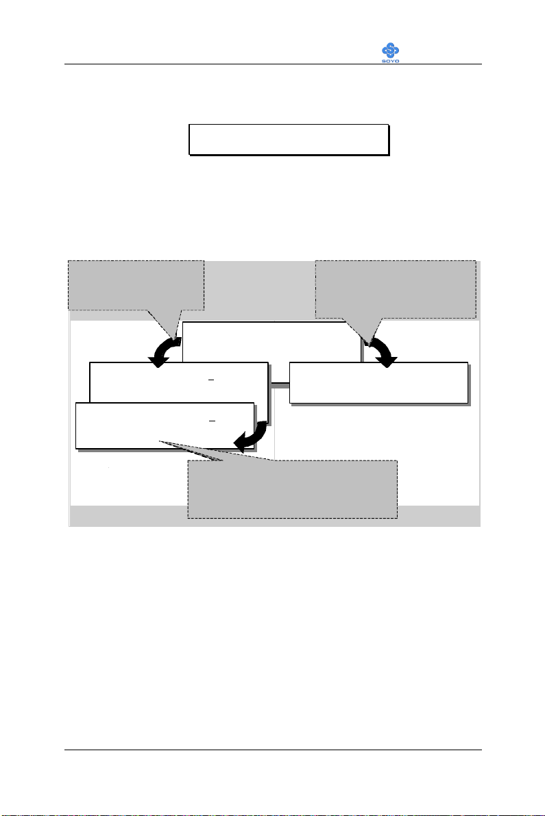
BIOS Setup Utility SY-7VDA
F10
(Shift) F2
↔
Type the Password
Press:
password, press
to exit
Type the Password
Press <Enter> without
After you confirm the password,
3. Enter your new password and press [Enter]. The following message
appears, prompting to confirm the new password:
Confirm Password:
4. Re-enter your password and then press [Enter] to exit to the Main
Menu.
This diagram outlines the password selection procedure:
and Press: <Enter>
↔
STANDARD CMOS SETUP
BIOS FEATURES SETUP
CHIPSET FEATURES SETUP
Enter Password:
POWER MANAGEMENT SETUP
PNP/PCI CONFIGURATION
Confirm Password:
LOAD SETUP DEFAULTS
LOAD BIOS DEFAULTS
Esc
: Quit
: Save & Exit Setup
CMOS SETUP UTILITY
AWARD SOFTWARE, INC.
Enter Password:
∗∗∗∗∗
∗∗∗∗∗
After you confirm the
press <Esc> to exit
Time, Date, Hard Disk Type…
ROM PCI/ISA BIOS
Press:
entering the password
Without entering password
INTEGRATED PERIPHERALS
SUPERVISOR PASSWORD
USER PASSWORD
Password Disabled!!
IDE HDD AUTO DETECTION
SAVE & EXIT SETUP
EXIT WITHOUT SAVING
↑ ↓ → ←
°
: Select Item
: Change Color
3-12 SET USER PASSWORD
When the user password option is on, you are not allowed to change any
setting in the [CMOS SETUP UTILITY] except for changing the user's
password.
The password setting procedure is similar to that for the [SUPERVISOR
PASSWORD] (Refer to section 3-9).
93
Page 98
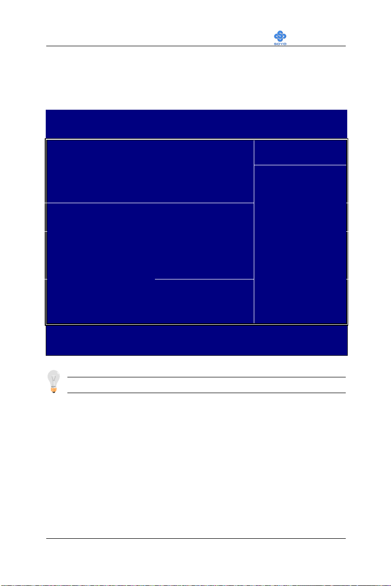
BIOS Setup Utility SY-7VDA
3-13 IDE HDD AUTO DETECTION
This Main Menu function automatically detects the hard disk type and
configures the [Standard CMOS Features] accordingly.
CMOS Setup Utility – Copyright ( C ) 1984-2001 Award Software
IDE Primary Master
IDE HDD Auto-Detection Press Enter
IDE Primary Master Auto
Capacity 0 MB
Access Mode Auto
0
Cylinder 0
Head 0
Precomp 0
Landing Zone 0
Sector 0
áâà:Move Enter:Select +/-/PU/PD:Value F10:Save ESC:Exit F1:General Help
F5:Previous Values F6:Fail-Safe Defaults F7: Optimized Defaults
Item Help
Menu Level 4
Note: This function is only valid for IDE type of hard disk drives.
94
Page 99

BIOS Setup Utility SY-7VDA
== Select a Boot First device ==
Boot Menu
Boot Menu enables user to boot-up on different boot device without going into the BIOS
setup.
To enable boot Menu, press “ESC” after memory initialization, user will
see a device menu, in which user can choose the device they wish to boot
from.
Boot Menu
Floppy
Ls120
HDD-0
SCSI
CDROM
HDD-1
HDD-2
HDD-3
ZIP100
LAN
:Move ENTER:Accept F4:Exit
95
Page 100
Drivers installation SY-7VDA
Chapter 4
DRIVERS INSTALLATION
The SOYO-CD will NOT autorun if you use it on an Operating
System other than Windows 9x or NT.
Your SY-7VDA Motherboard comes with a CD-ROM labeled "SOYO
CD." The SOYO CD contains (1) the user's manual file for your new
Motherboard, (2) the drivers software available for installation, and (3) a
database in HTML format with information on SOYO Motherboards and
other products.
Step 1. Insert the SOYO CD into the CD-ROM drive
If you use Windows NT, the SOYO-CD will not detect your motherboard
type. In that case the following dialog will pop up, please choose your
motherboard and press OK. Now the SOYO-CD Start Up Menu will be
shown.
Please Select Your Board
7IWA-F
7IWA-F V1.0
6IWM/L
6IWM
6IWA
OK
(SOYO CD Start Up Program Menu)
If you use Windows 95 or 98, the SOYO CD Start Up Program
automatically detects which SOYO Motherboard you own and displays the
corresponding model name.
96
LI-7000
7IWB
7IWB V1.0
7IWM
7IWM/L V1
Cancel
X
 Loading...