

“j
p=l
Pentium

SOYO
’”
About This Guide
This User’s Guide is for assisting system manufacturers and end users in setting up and
installing the
rnainboard. Information
in this guide has been carefully checked for
reliability;
however, no guarantee is given as to the correctness of the contents. The information in this
document is subject to change without notice,
Copyright Notice
Copyright
1996,
Soyo Computer Inc.
All
rights reserved. This manual is copyrighted by Soyo
Computer Inc. You
may
not reproduce, transmit, transcribe, store in a retrieval system, or
translate into any language, in any form or by any means, electronic, mechanical, magnetic,
optical, chemical, manual, or otherwise, any part of this publication without express written
permission of Soyo Computer Inc.
Trademarks
Soyo is a registered trademark of Soyo Computer Inc. AU trademarks are the property of their
owners.
Disclaimer
Soyo Computer Inc. makes no representations or warranties regarding the
contents
of this
manual. We reserve the right to revise the manual or make changes in the specifications of the
product described within it at any time without notice and without obligation to notify any
person of such revision or change. The information contained in this manual is provided for
general use by our customers. Our customers should be aware that the personal computer
field is the subject of many patents. Our customers should ensure that they take appropriate
action so that their use of our products does not infringe upon any patents. It is the policy of
Soyo Computer Inc. to respect the valid patent rights of third parties and not to infringe upon
or assist others to infringe upon such rights.
Restricted Rights Legend
Use, duplication, or disclosure by the Government is subject to restrictions set forth in
subparagraph (c)( I)(ii) of the Rights in Technical Data and Computer Software clause at
252.277-7013.
Product Rights
Product mentioned m this manual are mentioned for identification purpose
only.
Product
names appearing in this manual may or may not be registered trademarks or copyrights of
their respective companies
If you need any further information, please come to our home page on internet. The
address is
"http://www.soyocom.tw"
ttp//vmvw.soyo.com.tw”
Edition:
January 1996
Version 1.0
5S M2/M5 SERIAL
100% :w%:::,~
Visit SOYO On-Line at http
//www. soyo.
com.t w

Table of Contents
Chapter 1: Introduction
. . . . . . . . . . . . . . . . . . . . . . . . . . . . . . . . . . .
. .
. . . . . . . . . . . . .1
.
Key Features . . . . . . . . . . . . . . . . . . . . . . . . . . . . . . . . . . . . . . . . . . . . . . . . . . . . . . . . . . . . . . . . . . . . . . . . . . . . . . . . . . . . . . . . . . . . . . . . . . . . 1
Mainboard Layout w/ default settings* . . . . . . . . . . . . . . . . . . . . . . . . . . . . . . . . . . . . . . . . . . . . . . . . . . . . . . . . . . . 2
Onboard VGA Chip Features
(Optional)
. . . . . . . . . . . . . . . . . . . . . . . . . . . . . . . . . . . . . . . . . . . . . . . . . . . . . . . . 4
Unpacking the
Mainboard
. . . . . . . . . . . . . . . . . . . . . . . . . . . . . . . . . . . . . . . . . . . . . . . . . . . . . . . . . . . . . . . . . . . . . . . . . . . . . . . 4
Resolutions Supported . . . . . . . . . . . . . . . . . . . . . . . . . . . . . . . . . . . . . . . . . . . . . . . . . . . . . . . . . . . . . . . . . . . . . . . . . . . . . . 5
Electrostatic Discharge Precautions . . . . . . . . . . . . . . . . . . . . . . . . . . . . . . . . . . . . . . . . . . . . . . . . . . . . . . . . . . . . . . . .
5
Chapter 2: Hardware Setup
. . . . . . . . . . . . . . . . . . . . . . . . . . . . . . . . . . ● . . . . . . . . . ...0... ● . . . . .
6
Jumpers
. . . . . . . . . . . . . . . . . . . . . . . . . . . . . . . . . . . . . . . . . . . . . . . . . . . . . . . . . . . . . . . . . . . . . . . . . . . . . . . . . . . . . . . . . . . . . . . . . . . . . . . . . . . .
6
Factory Set Jumpers . . . . . . . . . . . . . . . . . . . . . . . . . . . . . . . . . . . . . . . . . . . . . . . . . . . . . . . . . . . . . . . . . . . . . . . . . . . . . . . . . .
6
JP25:
Sleep Switch Connector Enable/Disable . . . . . . . . . . . . . . . . . . . . . . . . . . . . . . . . . . . . . . . . .
6
JP3: Display
Type
. . . . . . . . . . . . . . . . . . . . . . . . . . . . . . . . . . . . . . . . . . . . . . . . . . . . . . . . . . . . . . . . . . . . . . . . . . . . . . . . . . . . . 7
JP5:
CMOS
Clear
Jumper . . . . . . . . . . . . . . . . . . . . . . . . . . . . . . . . . . . . . . . . . . . . . . . . . . . . . . . . . . . . . . . . . . . . . . . . . . . 7
JP33:
Pipeline Select .. . . . . . . . . . . . . . . . . . . . . . . . . . . . . . . . . . . . . . . . . . . . . . . . . . . . . . . . . . . . . . . . . . . . . . . . . . . . . . . 7
JP34:
L1 Write-Back /Write-Through Cache Select . . . . . . . . . . . . . . . . . . . . . . . . . . . . . . . . . 8
JP46:
VRM (Voltage Regulator Module)
Socket
(Optional) . . . . . . . . . . . . . . . . . . . . . 8
JPS2: PS/2Mouse
Function
Jumper . . . . . . . . . . . . . . . . . . . . . . . . . . . . . . . . . . . . . . . . . . . . . . . . . . . . . . . . . . 8
JP38, JP42:
Bus Fraction Core/Bus Ratio Select . . . . . . . . . . . . . . . . . . . . . . . . . . . . . . . . . . . . . . . .
9
JP40:
CPU Burst Mode
Select
. . . . . . . . . . . . . . . . . . . . . . . . . . . . . . . . . . . . . . . . . . . . . . . . . . . . . . . . . . . . . . . . . . 10
CPU
Type Configuration
. . . . . . . . . . . . . . . . . . . . . . . . . . . . . . . . . . . . . . . . . . . . . . . . . . . . . . . . . . . . . . . . . . . . . . . . . . . . . . . 10
JP43~JP45:
CPU
Voltage Select......
. . . . . . . . . . . . . . . . . . . . . . . . . . . . . . . . . . . . . . . . . . . . . . . . . .
13
Memory Configuration . . . . . . . . . . . . . . . . . . . . . . . . . . . . . . . . . . . . . . . . . . . . . . . . . . . . . . . . . . . . . . . . . . . . . . . . . . . . . . . . . .
14
Cache
Configu
ration . . . . . . . . . . . . . . . . . . . . . . . . . . . . . . . . . . . . . . . . . . . . . . . . . . . . . . . . . . . . . . . . . . . . . . . . . . . . . . . . . . . . . .
14
Cache Size and RAM
Locations
. . . . . . . . . . . . . . . . . . . . . . . . . . . . . . . . . . . . . . . . . . . . . . . . . . . . . . . . . . . . . . . 14
Multi 1/0
Port
Addresses . . . . . . . . . . . . . . . . . . . . . . . . . . . . . . . . . . . . . . . . . . . . . . . . . . . .. . . . . . . . . . . . . . . . . . . . . . . .
16
Connectors . . . . . . . . . . . . . . . . . . . . . . . . . . . . . . . . . . . . . . . . . . . . . . . . . . . . . . . . . . . . . . . . . . . . . . . . . . . . . . . . . . . . . . .. . . . . . . .
16
J1-PS/2 Mouse Connector . . . . . . . . . . . . . . . . . . . . . . . . . . . . . . . . . . . . . . . . . . . . . . . . . . 16
J3-Keyboard Connector . . . . . . . . . . . . . . . . . . . . . . . . . . . . . . . . . . . . . . . . . . . . . . . . . . . . . . . . . . . . . . . . . .
16
J4-Power Supply Connectors . . . . . . . . . . . . . . . . . . . . . . . . . . . . . . . . . . . . . . . . . . . . . . . . . . . . . . . . . . . . . . 16
J17-Keylock
& Power LED Connector . . . . . . . . . . . . . . . . . . . . . . . . . . . . . . . . . . . . . . . . . . . . . . . . . 17
J18-Speaker
Connector . . . . . . . . . . . . . . . . . . . . . . . . . . . . . . . . . . . . . . . . . . . . . . . . . . . . . . . . . . . . . . . . . . . . 17
JP19-Hardware Reset
Control. . . . . . . . . . . . . . . . . . . . . . . . . . . . . . . . . . . 17
J20-External Battery Connector
. . . . . .. . . . . . . . . . . . . . . . . . . . . . . . . . . . .
17
J22-Turbo LED Connector ..
...... . . . . . . . . . . . . . . . . . . . . . .
17

IDE1/IDE2
- On-board Primary/Secondary IDE HDD Connectors . . . . . . 17
LED1/LED2– HDD
LED Connectors . . . . . . . . . . . . . . . . . . . . . . . . . . . . . . . . . . . . . . . . . . . . . . . . . . . . . 17
COM1/COM2 Connectors
. . . . . . . . . . . . . . . . . . . . . . . . . . . . . . . . . . . . . . . . . . . . . . . . . . . . . . . . . . . . . . . . . . . . . . .
18
FDC Connector
. . . . . . . . . . . . . . . . . . . . . . . . . . . . . . . . . . . . . . . . . . . . . . . . . . . . . . . . . . . . . . . . . . . . . . . . . . . . . . . . . . . . . . .
18
PRT1 Connector
. . . . . . . . . . . . . . . . . . . . . . . . . . . . . . . . . . . . . . . . . . . . . . . . . . . . . . . . . . . . . . . . . . . . . . . . . . . . . . . . . . . . . .
18
VGA
Connector (Optional)
. . . . . . . . . . . . . . . . . . . . . . . . . . . . . . . . . . . . . . . . . . . . . . . . . . . . . . . . . . . . . . . . . . . .
18
VGA
Feature Connector (Optional) . . . . . . . . . . . . . . . . . . . . . . . . . . . . . . . . . . . . . . . . . . . . . . . . . . . . . . .
18
AUDIO Connector . . . . . . . . . . . . . . . . . . . . . . . . . . . . . . . . . . . . . . . . . . . . . . . . . . . . . . . . . . . . . . . . . . . . . . . . . . . . . ...18
JP52-
Wave Table Connector . . . . . . . . . . . . . . . . . . . . . . . . . . . . . . . . . . . . . . . . . . . . . . . . . . . . . . . . . . . . . . . . 18
Audio Adapter Function . . . . . . . . . . . . . . . . . . . . . . . . . . . . . . . . . . . . . . . . . . . . . . . . . . . . . . . . . . . . . . . . . . . . . . . . . . . . . . . .
19
WTC1-Wave
Table Card Connector . . . . . . . . . . . . . . . . . . . . . . . . . . . . . . . . . . . . . . . . . . . . . . . . . . . . 19
SB1- Audio
Adapter
Connector
. . . . . . . . . . . . . . . . . . . . . . . . . . . .. . . . . . . . . . . . . . . . . . . . . . . . . . . . . . .
19
J1-CD-ROMAudio
In Connector . . . . . . . . . . . . . . . . . . . . . . . . . . . . . . . . . . . . . . . . . . . . . . . . . . . . . . . . .
19
JACK1
- Speaker Out Jack
. . . . . . . . . . . . . . . . . . . . . . . . . . . . . . . . . . . . . . . . . . . . . . . . . . . . . . . . . . . . . . . . . . . . . .
19
JACK2-Line
Out
Jack . . . . . . . . . . . . . . . . . . . . . . . . . . . . . . . . . . . . . . . . . . . . . . . . . . . . . . . . . . . . . . . . . . . . . . . . . . . .
19
JACK3- Line In
Jack . . . . . . . . . . . . . . . . . . . . . . . . . . . . . . . . . . . . . . . . . . . . . . . . . . . . . . . . . . . . . . . . . . . . . . . . . . . . . . .
19
JACK4-
MC
In
Jack . . . . . . . . . . . . . . . . . . . . . . . . . . . . . . . . . . . . . . . . . . . . . . . . . . . . . . . . . . . . . . . . . . . . . . . . . . . . . . .
19
DB15
– Game Port Connector
. . . . . . . . . . . . . . . . . . . . . . . . . . . . . . . . . . . . . . . . . . . . . . . . . . . . . . . . . . . . . . . .
19
Chapter 3: BIOS Setup
. . . . . . . . . . . . . . . . . . . . . . . . . . . . . . . . . . . . . . . . . . . . . . . .
....
21
Standard CMOS Setup . . . . . . . . . . . . . . . . . . . . . . . . . . . . . . . . . . . . . . . . . . . . . . . . . . . . . . . . . . . . . . . . . . . . . . . . . . . . . . . . . . . 22
BIOS Features
Setup
. . . . . . . . . . . . . . . . . . . . . . . . . . . . . . . . . . . . . . . . . . . . . . . . . . . . . . . . . . . . . . . . . . . . . . . . . . . . . . . . . . . . . . 23
Chipset Features
Setup
. . . . . . . . . . . . . . . . . . . . . . . . . . . . . . . . . . . . . . . . . . . . . . . . . . . . . . . . . . . . . . . . . . . . . . . . . . . . . . . . . . 25
Power Management Setup
. . . . . . . . . . . . . . . . . . . . . . . . . . . . . . . . . . . . . . . . . . . . . . . . . . . . . . . . . . . . . . . . . . . . . . . . . . ...27
PCI Configuration
Setup
. . . . . . . . . . . . . . . . . . . . . . . . . . . . . . . . . . . . . . . . . . . . . . . . . . . . . . . . . . . . . . . . . . . . . . . . . . . . . . . . 29
Load Setup Defaults . . . . . . . . . . . . . . . . . . . . . . . . . . . . . . . . . . . . . . . . . . . . . . . . . . . . . . . . . . . . . . . . . . . . . . . . . . . . . . . . . . . . . . . 32
Supervisor
Password . . . . . . . . . . . . . . . . . . . . . . . . . . . . . . . . . . . . . . . . . . . . . . . . . . . . . . . . . . . . . . . . . . . . . . . . . . . . . . . . . . . . . 33
User Password . . . . . . . . . . . . . . . . . . . . . . . . . . . . . . . . . . . . . . . . . . . . . . . . . . . . . . . . . . . . . . . . . . . . . . . . . . . . . . . . . . . . . . . . . . . . . . . 33
IDE HDDAuto
Detection . . . . . . . . . . . . . . . . . . . . . . . . . . . . . . . . . . . . . . . . . . . . . . . . . . . . . . . . . . . . . . . . . . . . . . . . . . . . .
34

1 Introduction
The
SiS
551X / P54C
PCI
ma inboard is a high-performance system board that
supports
Pentium
P54CX and
Cyrix
6x86 family
CPUs.
You can install 256K to 512K
of external cache memory on the
mainboard.
The
mainboard
is fully compatible
with industry standards, and adds many technical enhancements.
Key Features
●
●
●
●
●
●
●
●
●
●
●
●
●
●
Supports
P54CX
family CPU running at 75/90/100/120/133/150/166/180/200
MHz speed and
Cyrix
6x86 CPU running at 100/120/133/MHz speed.
Supports SOCKET
7 &
VRM
for upgrade (optional)
Integrated Second Level
(L2)
Cache Controller
(256K/512K)
“
—
Write Through and Write Back Cache Modes
—
Direct Mapped Organization
—
On-board Pipeline Burst
SRAMs
Cache and
Pipelined
Burst module
slot support.
Integrated DRAM Controller
—
Concurrent Write Back
—
CAS#-before-RAS#
Transparent DRAM Refresh
—
256K,
512K, lM,
2M, 4M, or 16M x N 70ns Fast Page and EDO
DRAM
(symmetric and asymmetric)
—
On-board memory configurations from 2 to 512 Mbytes
—
Supports single 32 bits SIMM for booting and operating on SIMM 2
and SIMM 4
Supports
CPU
Stop
Clock
Supports "Table-Free
"
DRAM
configuration
Compliant to PCI specifications
v2.O
Three 32-bit PCI slots (Masters) and Three ISA slots, 4-layer PCB
System BIOS built-in NCR81O SCSI Card BIOS and
"Plug and Play"
function
On-board built-in PCI Master IDE controller and floppy controller
On-board supports for two high speed UARTS (w/i 16550 FIFO) and
Multimode parallel port for Standard, Enhanced (EPP) and high speed (ECP)
modes, and
supports PS/2 mouse function
On-board supports FLASH Memory for easy upgrade BIOS
On-board
SVGA
function and
attaching software
MPEG (optional)
On-board
built-in
Creative
CT-2504
’-
25O4
sound chip (optional)
2
Introduction
Mainboard
Layout
w/ default settings*
n Ii
n nl.k3F+@l
I
~
1
7
.
PHJLHJ y]
p
’f’q
ll,,,
Figure
1-1.
Mainboard Layout
1.
P54 in
ZIF
socket
7
12.
2
3.
4.
5.
6.
7.
8.
9.
10.
11.
Pipelined
Burst SRAM
Sis 551X
Chipset
Pipelined
Burst SKAM Module Slot
PnP
FLASH BIOS
Audio
Chipset
ISA
Slots
PCI Slots
SIMM Memory Bank
5V DC
Power
Connector
Keyboard
Connector
13.
14
15.
16.
17.
18.
19.
20,
21
U
PS/2 Mouse Connector
IDE1/IDE2
Connector
Floppy Connector
Parallel
Port
Connector
COM1/COM2
connector
Keyboard BIOS
super
I/O
Chipset
VGA Connector
(optional)
VGA Feature
Connector (optional)
Audio
Connector
Wave Table Connector
Introduction
3
Refer to Figure 1-2 for the
mainboard
layout and the default settings areas follows:
Pentium 100MHz CPU, 256K W/B Pipelined Burst cache, Address Pipeline Enabled,
On-board EIDE Enabled (PIO Mode), FDD Enabled, 2 high speed UART Enabled
(w/ 16550 FIFO), 1
EPP/ECP
port (standard mode), and PS/2 Mouse Disabled.
1-111111-1111
$?2
. .
I
I
SA
SLOT
LPr
mii
JP48
II
D[u[
PCI SLOT
65
mm
N-
Wave Table
Connector
Eh-Ei
’m
”
IT
5512
m
35
o“
El
CPU
m
—
1
Important:
Make sure the system is
well
ventilated to prevent
overheating and ensure system stability.
*Note:
SIMM2
and
SIMM
4
can install
single32
bits SIMM.

4
Introduction
Onboard VGA Chip Features (Optional)
●
●
●
●
●
●
●
●
Supports
share memory for both system memory and display memory
Supports 32 bit
PCI local bus standard revision 2.1
Supports
PCI
multimedia design
guide
revision 1.0
Supports 32/64 bit display memory path
Supports VESA DPMS compliant VGA monitor for power
management
Supports resolution up to 1280 x 1024256
colors(NI)
or 1280x 102464K colors
(Interlace only)
Supports virtual screen up to
2048 x 2048
Supports
sofiware
MPEG function.
Resolutions Supported
Resolution
1 MByte DRAM* 2 MByte DRAM*
640x480x256
I
I
640x480x64K
I
I
640x480x16M
I
I
800X600X16
I
I
800X600X256
I
800X600X64K
I
I
800X600X16M
I
x
I
l/
1024x768x16
I
I
1024x768x2%
I
I
1024x768x64K
x
J
1024x768x16M
x
x ’
128OX1O24X16
/
d
128OX1O24X256
x
J
This size is controlled
by
BIOS and shared with the system main
memory.
Note:
The VGA online manual can be found in VGA diskettes 1 under the
"MANUAL" subdirectory.

Introduction
5
Unpacking the
Mainboard
The
mainboard
package contains:
●
The
SiS
551X / P54C
Mainboard
●
This User's Guide
Note: Do not unpack the
mainboard until you
are ready to install it.
Follow the precautions below while unpacking the
mainboard,
1.
2.
3.
Before handling the
mainboard,
ground yourself by grasping an unpainted
portion of the system's metal chassis.
Remove the
mainboard
from its anti-static packaging and place it on a grounded
surface, component side up.
Check the
mainboard
for damage. If any chip appears loose, press carefully to
seat it
firmly
in its socket.
Do not apply power if the
rnainboard
appears damaged. If there is damage to the
board contact your dealer immediately.
Electrostatic Discharge Precautions
Make sure you ground yourself before handling the
mainboard
or other system
components. Electrostatic discharge can easily darnage the components. Note that
you must take special precaution when handling the
mainboard
in dry or
air-
conditioned environments.
Take these precautions to protect your equipment from electrostatic discharge:
● Do not remove the anti-static packaging until you are ready to install the
rnainboard
and other system components.
●
Ground yourself before removing any system component from its protective
anti-static packaging. To ground yourself grasp the expansion slot covers or
other unpainted portions of the computer chassis.
●
Frequently ground yourself while working, or use a grounding strap.
●
Handle the
rnainboard
by the edges and avoid touching its components.

2
Hardware Setup
This chapter explains how to configure the
mainboard
's
’s
hardware. After you install
the
mainboard,
you can set jumpers, install memory on the
mainboard,
and make
case connections. Refer to this chapter whenever you upgrade or reconfigure your
system.
CAUTION:
Turn
off power
to the
mainboard,
system
chassis, and
peripheral devices
before performing
any work on
the
mainboard
or
system
Jumpers
Factory Set Jumpers
'
The following jumpers are set at the factory as below. -
Jumpers
Factory settings
JP28, JP29, JP31, JP36,
JP37,
Factory fixed at Short
JP47
J21
Reserved
JP5,
JP34,
JP48,
JP53,
JP50,
Factory setting at
1-2
JP51
JP28, JP29, JP32, JP33,
JP47
Factory setting at 2-3
JP30
Factory freed at
3-5
and 4-6
JP25:
Sleep Switch Connector
Enable/Disable
Toggle this jumper to force the system into power saving (Green) mode. Any
hardware IRQ signal makes the system
wakeups.
8
Hardware Setup
JP34:
11 Write-Back /Write-Through Cache Select
Set JP34 to configure the
mainboard
for L1 Write-Back/Write-Through Cache.
11 Cache
JP34
Write Back Cache
(default)
m
123
Write Through Cache
m
123
JP46:
VRM (Voltage Regulator Module) Socket (Optional)
VRM socket
is dedicated for 2.5V
CPU to use. It converts 3.3V to 2.5V for the
advance high speed
P54CX.
JPS2: PS/2
Mouse Function Jumper
Set PS/2 mouse function enabled or disabled.
PS/2 Mouse Function
JPS2
Disabled
m
(default)
12
Enabled
=
12
Note: The
IRQ12
is dedicated to PS/2 mouse when choose enabled of
PS/2
Mouse
Function.
Hardware Setup
9
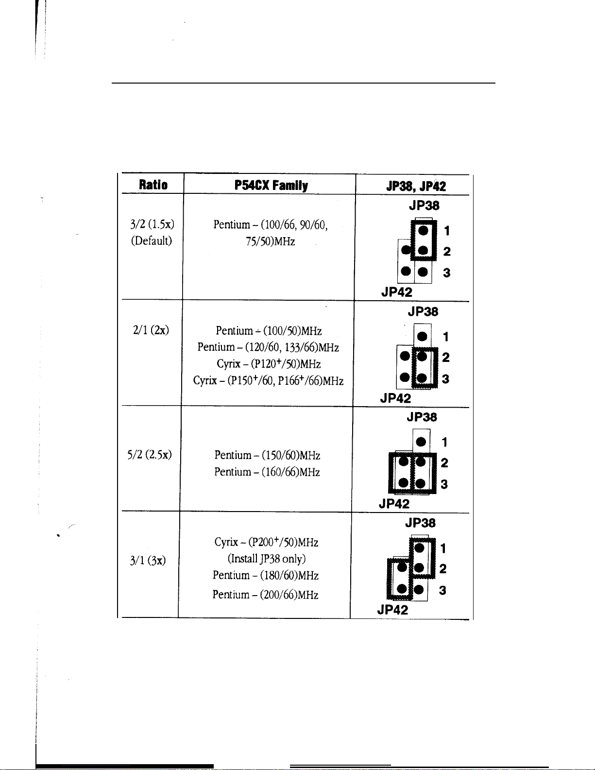
JP38,
JP42:
Bus Fraction Core/Bus Ratio
Select
Set this
jumper
according to your CPU clock and this setting is only for
Pentium.
Note: For
PentiumX
/Y MHz, X stands for CPU core clock, Y stands for bus clock.
 Loading...