

Page 1

Working Instruction, Electrical
Working Instruction, Electrical
Applicable for W380, Z555
CONTENTS
1 Read this first! ........................................................................................2
2 Lead-free soldering ................................................................................3
3 BGA equipment reflow profiles............................................................. 5
3.1 General.................................................................................................. 5
3.2 Temperature Measurements ................................................................. 5
3.3 Reflow Profiles ...................................................................................... 6
4 Replacement of components ................................................................6
4.1 Liquid Intrusion Indicator: ...................................................................... 7
4.2 System Connector Gaskets:.................................................................. 7
4.3 E1002 Bluetooth Shield Can: ................................................................ 8
4.4 X0616: Battery Connector ..................................................................... 9
4.5 X2600: System Connector .................................................................. 10
4.6 X2600: System Connector Continued ................................................. 11
4.7 Revision History .................................................................................. 12
1208-3979 1
© Sony Ericsson Mobile Communications AB
Page 2

Working Instruction, Electrical
1 Read this first!
• Before you start replacing any components, make sure you have read and fully understood
the contents of section 2 and 3!
• Also make sure you have access to the Mechanical Working Instruction and the Equipment
Lists described on the first page of section 4!
• Use Electrostatic Discharge (ESD) equipment to avoid damaging the PBA.
• Use gloves or finger cots to avoid contaminating the PBA with skin oil.
1208-3979 1
© Sony Ericsson Mobile Communications AB
2(12)
Page 3
Working Instruction, Electrical
2 Lead-free soldering
THIS PRODUCT IS MANUFACTURED WITH LEAD-FREE SOLDER
AND LEAD
During electrical repair, it is critical to make sure that no lead is
introduced.
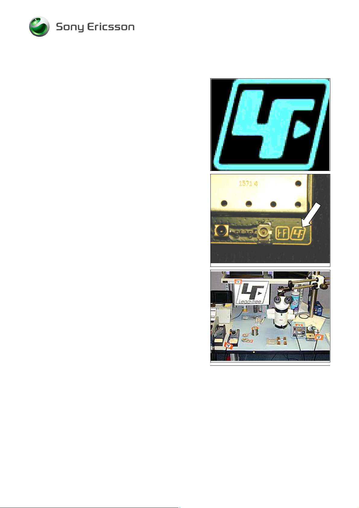
This symbol indicates that the product is lead- free.
-FREE COMPONENTS!
The lead-free symbol is located on the PCB as shown.
A lead-free work area must be set up completely separated
from work areas that are used to make lead repairs. The leadfree work area must also be clearly labeled with the lead free
symbol as shown in the adjacent picture. The items on this
desk must remain lead-free. They must be adequately labeled
to make their lead-free status clearly and easily recognized.
1208-3979 1
© Sony Ericsson Mobile Communications AB
3(12)
Page 4
Working Instruction, Electrical
Lead-free soldering continued
LFS (lead-free solder) characteristics:
• High melting point (typically 217°C)
• Low wetting
• High surface tension
• Difficult to spread
• Recommended tip temperature = 370°C
WHEN SERVICING PBAS THAT HAVE BEEN MANUFACTURED
WITH
LFS (LEAD-FREE SOLDER), LFS MUST BE USED!
F NOT, THERE IS A HIGH RISK OF UNRELIABLE SOLDERING
I
JOINTS
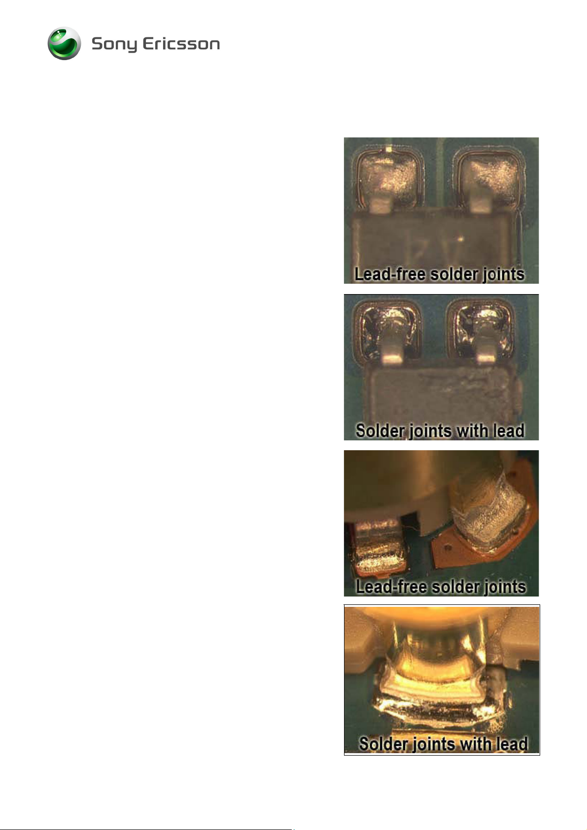
Lead-free solder joints are more difficult to inspect because they
do not have shiny surfaces like leaded solder joints. Also, leadfree solder does not flow as well as leaded solder, so some of
the solder pad areas may remain exposed.
!
1208-3979 1
© Sony Ericsson Mobile Communications AB
4(12)
Page 5

Working Instruction, Electrical
3 BGA equipment reflow profiles
3.1 General
This section contains reflow profile recommendations for mobile phones and similar products.
They are just general recommendations and considerations have to be taken for every single product.
The solder is secondary but could also affect the parameters.
In this document one alloy is specified: SnAgCu (Lead free) melting point 217°C
3.2 Temperature Measurements
At least four probes should be used.
They should be placed on components with the highest and lowest thermal mass.
The probes shall be located in the beginning, in the middle and at the end of the board/panel.
It is recommended that the probes are soldered on the board, but glue and Kapton tape can be used.
At least one probe shall be placed in the air or on top of a component.
These values are strongly depending on the BGA replacement equipment.
A nozzle type will be chosen based on the outer size of the actual component.
Make sure the nozzle does not affect any nearby placed components.
HESE VALUES ARE RECOMMENDATIONS AND MAY HAVE TO BE CHANGED DEPENDANT ON THE TYPE OF
T
EQUIPMENT
HE MAXIMUM TEMPERATURE FOR ANY COMPONENT MUST NOT EXCEED 260°C!
T
!
1208-3979 1
© Sony Ericsson Mobile Communications AB
5(12)
Page 6

Working Instruction, Electrical
3.3 Reflow Profiles
Sn/Ag/Cu (lead-free)
Ramp rate < 4°C/sec
Ramp rate cooling zone < 6°C/sec
Time above liquidus 60-150 sec
Minimum temperature 235°C
Maximum temperature 245°C or 260°C for 10 sec. (the higher
temperature in case the board has
extremely high ΔT)
Bottom heat temperature 125°C-150°C
Total time Approx. 4-7 min
4 Replacement of components
CAUTION
• Keep all contact surfaces clean of dirt and hand-grease!
EQUIPMENT
For equipment information, refer to the Electrical and Mechanical Equipment Lists.
MECHANICAL INSTRUCTIONS
For phone disassembly and reassembly information, refer to the Mechanical Working Instruction.
1208-3979 1
© Sony Ericsson Mobile Communications AB
6(12)
Page 7

Working Instruction, Electrical
4.1 Liquid Intrusion Indicator:
If the liquid Intrusion indicator is damaged or missing, or if
the shield lid on E1004 is replaced, then place a new liquid
intrusion indicator on the shield lid in the position shown.
The indicator should be at the left edge of the lid and
centered between the top and middle holes.
4.2 System Connector Gaskets:
Before repairing parts near the system connector, remove
the system connector gaskets.
Use tweezers to pull the gaskets out of the holes.
After the PCB cools, replace the gaskets as shown.
Position the gaskets such that the amount extending on
each side of the PCB is approximately equal.
1208-3979 1
© Sony Ericsson Mobile Communications AB
7(12)
Page 8

Working Instruction, Electrical
4.3 E1002 Bluetooth Shield Can:
The Bluetooth module is located under a one-piece shield
can. Apply heat-resistant tape to the adjacent components.
Use a large hot air device to remove the shield.
1208-3979 1
© Sony Ericsson Mobile Communications AB
8(12)
Page 9

Working Instruction, Electrical
4.4 X0616: Battery Connector
Apply heat-resistant tape to protect the adjacent
components.
Use a large hot air device to reflow the solder.
Use tweezers to remove the component.
After placing the new part in position, use a soldering iron to
solder the leads.
1208-3979 1
© Sony Ericsson Mobile Communications AB
9(12)
Page 10

Working Instruction, Electrical
4.5 X2600: System Connector
Apply heat-resistant tape to the adjacent components.
Use a large hot air device to reflow the solder.
Remove the component.
The two through holes will have excess solder in them.
1208-3979 1
© Sony Ericsson Mobile Communications AB
10(12)
Page 11

Working Instruction, Electrical
4.6 X2600: System Connector Continued
Remove the solder from the through holes.
Place the new part on the board and solder the leads.
Turn the board over and solder the pegs in the holes.
1208-3979 1
© Sony Ericsson Mobile Communications AB
11(12)
Page 12

Working Instruction, Electrical
4.7 Revision History
Rev. Date Changes / Comments
1 2008-Feb-29 Initial Release
1208-3979 1
© Sony Ericsson Mobile Communications AB
12(12)
 Loading...