

Page 1

Working Instruction, Electrical
Working Instruction, Electrical
Applicable for K330
CONTENTS
Read this first!...................................................................................................2
1
2 Lead-free soldering...........................................................................................3
3 BGA equipment reflow profiles........................................................................5
3.1 General.................................................................................................. 5
3.2 Temperature Measurements ................................................................. 5
3.3 Reflow Profiles ...................................................................................... 6
4 Replacement of components...........................................................................7
4.1 Shielding Cover BB ............................................................................... 8
4.2 D12: TVS Diode 24V 50pF.................................................................... 9
4.3 D71: TVS Diode 12V 38pF................................................................... 9
4.4 D101: Protection DIODE ....................................................................... 9
4.5 J1: LCD ZIF Connector ....................................................................... 10
4.6 J2: SIM Connector............................................................................... 10
4.7 J4: Microphone.................................................................................... 10
4.8 J6: Battery Connector.......................................................................... 11
4.9 J7: Board to Board Connector (Keypad PCB)..................................... 11
4.10 U100: Illumination Pump ..................................................................... 11
4.11 U601: Audio Amplifier.......................................................................... 12
4.12 U606: FM Module................................................................................ 12
4.13 U706: Voltage Level Shifter................................................................. 12
4.14 U8: Charge IC ..................................................................................... 13
4.15 U9: IC Charging................................................................................... 13
4.16 Z1002: Camera Socket ....................................................................... 13
4.17 Z901: Antenna Connector ................................................................... 14
4.18 Z902: RF Connector............................................................................ 14
5 Revision history .............................................................................................. 15
1219-0637 Rev 2
Company Internal © Sony Ericsson Mobile Communications AB
Page 2

Working Instruction, Electrical
1 Read this first!
z Before you start replacing any components, make sure you have read and fully understood
the contents of section 2 and 3!
z Also make sure you have access to the mechanical Working Instruction and the equipment
listed on the first page of section 4!
1219-0637 Rev 2
Company Internal © Sony Ericsson Mobile Communications AB
2(15)
Page 3
Working Instruction, Electrical
2 Lead-free soldering
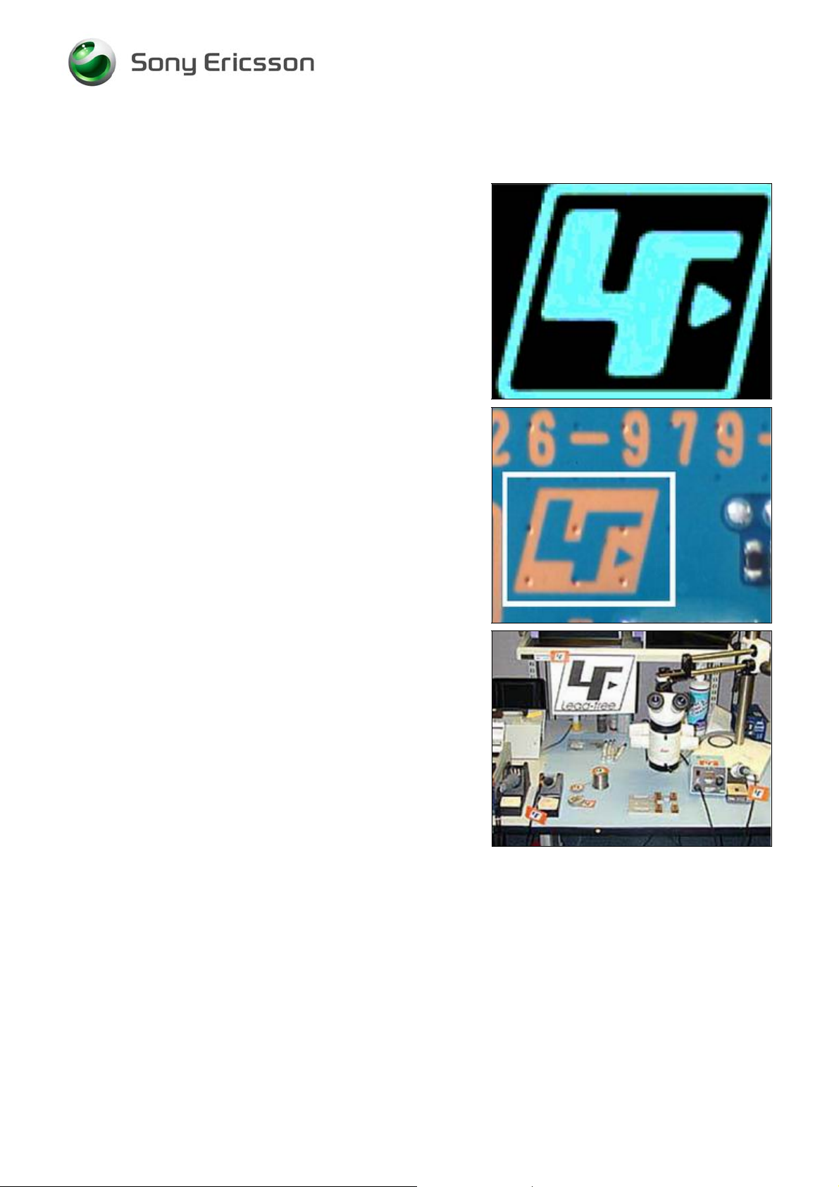
THIS PRODUCT IS MANUFACTURED WITH LEADFREE SOLDER AND LEAD-FREE COMPONENTS!
During electrical repair, it is critical to make sure that no
lead is introduced. This symbol indicates that the product
is lead- free.
All lead-free PBAs will be marked with this symbol.
A lead-free work area must be set up completely
separated from work areas that are used to make lead
repairs. The lead-free work area must also be clearly
labeled with the lead free symbol as shown in the
adjacent picture. The items on this desk must remain
lead-free. They must be adequately labeled to make their
lead-free status clearly and easily recognized.
1219-0637 Rev 2
Company Internal © Sony Ericsson Mobile Communications AB
3(15)
Page 4
Working Instruction, Electrical
Lead-free soldering continued
LFS (lead-free solder paste) characteristics:
z High melting point (typically 220°C)
z Low wet ability
z High surface tension
z Difficult to spread
z Recommended tip temperature = 370°C
WHEN SERVICING PBAS THAT HAVE BEEN
MANUFACTURED WITH LFS (LEAD-FREE SOLDER
PASTE), LFS MUST BE USED! IF NOT, THERE IS A
HIGH RISK OF UNRELIABLE SOLDERING
JOINTS!
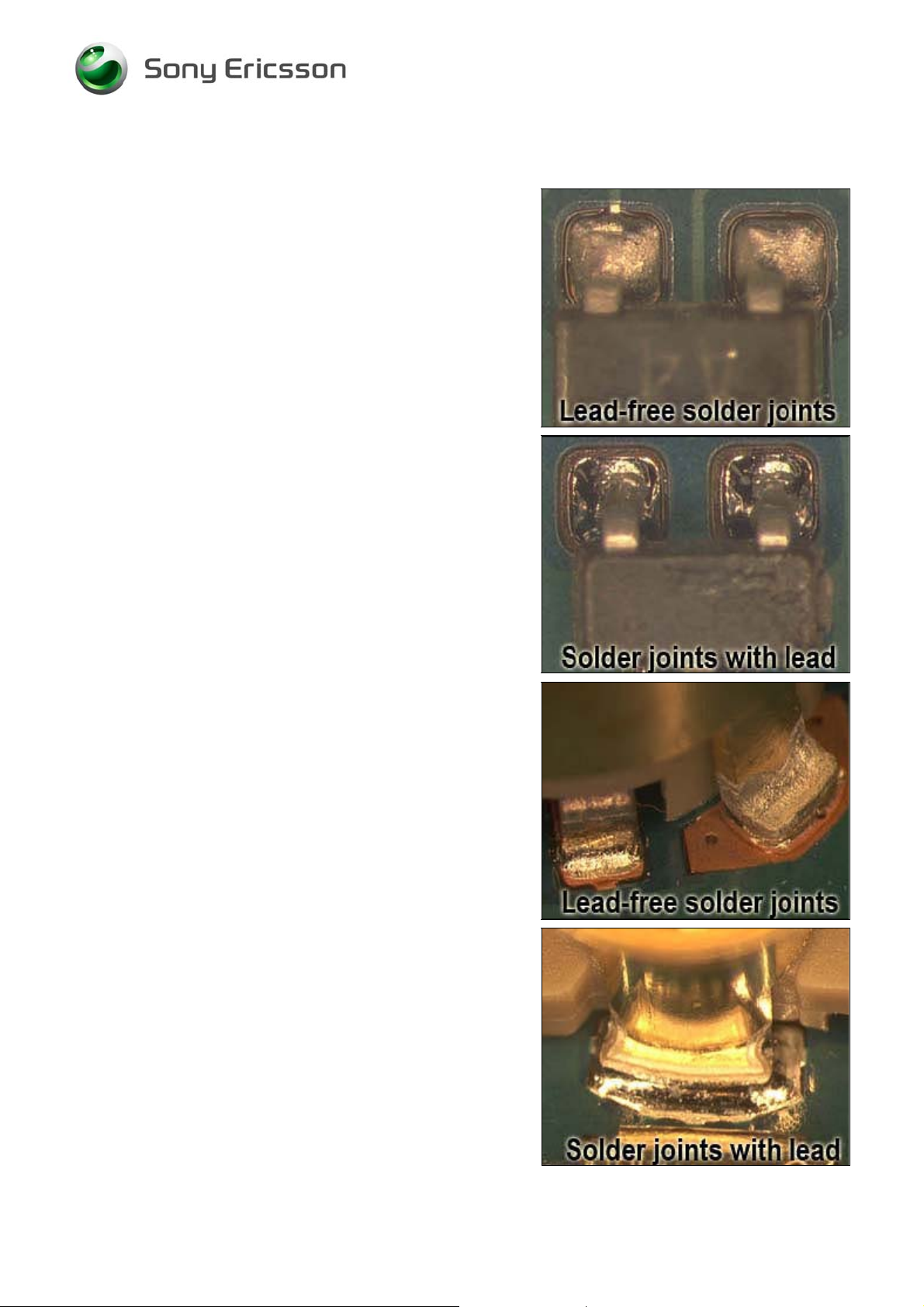
Lead-free solder joints are more difficult to inspect
because they do not have shiny surfaces like leaded
solder joints. Also, lead-free solder does not flow as well
as leaded solder, so some of the solder pad areas may
remain exposed.
1219-0637 Rev 2
Company Internal © Sony Ericsson Mobile Communications AB
4(15)
Page 5

Working Instruction, Electrical
3 BGA equipment reflow profiles
3.1 General
This document contains reflow profile recommendations for mobile phones and similar products.
They are just general recommendations and considerations have to be taken for every single product.
The solder paste is secondary but could also affect the parameters.
In this document one alloy is specified:
SnAgCu (Lead free) melting point 217°C
3.2 Temperature Measurements
At least four probes should be used.
They should be placed on components with the highest and lowest thermal mass.
The probes shall be located in the beginning, in the middle and at the end of the board/panel.
It is recommended that the probes are soldered on the board, but glue and capton tape can be used.
At least one probe shall be placed in the air or on top of a component.
These values are strongly depending on the BGA replacement equipment.
Nozzle type will be chosen after the outer size of the actual component.
Make sure the nozzle does not affect any nearby placed components.
THESE VALUES ARE RECOMMENDATIONS AND MAY HAVE TO BE CHANGED DEPENDING
ON THE TYPE OF EQUIPMENT!
THE MAXIMUM TEMPERATURE FOR ANY COMPONENT MUST NOT EXCEED 250°C!
1219-0637 Rev 2
Company Internal © Sony Ericsson Mobile Communications AB
5(15)
Page 6

Working Instruction, Electrical
3.3 Reflow Profiles
Sn/Ag/Cu (lead-free)
Ramp rate < 4°C/sec
Ramp rate cooling zone < 6°C/sec
Time above liquidus 60-150 sec
Minimum temperature 235°C
Maximum temperature 245°C or 260°C for 10 sec.
(the higher temperature in case the
board has extremely high ΔT)
Bottom heat temperature 125°C-150°C
Total time Approx. 4-7 min
1219-0637 Rev 2
Company Internal © Sony Ericsson Mobile Communications AB
6(15)
Page 7

Working Instruction, Electrical
4 Replacement of components
EQUIPMENT
z Dentist hook
z ESD-gloves (cotton gloves)
z ESD-wristband
z Soldering tool
z Hot air soldering station
z BGA replacement equipment
z Pair of tweezers
z Solder cleaning wiper (tin wick)
z Solder paste lead-free (SN 96% Ag 3.5% Cu 0.5%)
z Flux, RMA no-clean flux
z Cutting pliers
z Shield fence pliers NTZ 112 537
CAUTION
z Keep all contact surfaces clean of dirt and hand-grease!
MECHANICAL INSTRUCTIONS
For all the following part replacements, disassemble and assemble the phone as described in
Working Instruction 3/00021-1/FEA 209 544/X.
1219-0637 Rev 2
Company Internal © Sony Ericsson Mobile Communications AB
7(15)
Page 8
Working Instruction, Electrical
4.1 Shielding Cover BB
E CAREFUL NOT TO DAMAGE ANY COMPONENTS
B
SURROUNDING THE
Use minus screwdrivers to raise the corner of shielding
cover.
Continue with the same procedure on all other corners to
remove the Shielding Cover
SHIELDING FRAME!
USE A NEW SHIELDING COVER!
Press the shielding cover down to snap all hooks onto
shielding frame until you hear a ‘Click’ sound.
1219-0637 Rev 2
Company Internal © Sony Ericsson Mobile Communications AB
8(15)
Page 9

Working Instruction, Electrical
4.2 D12: TVS Diode 24V 50pF
REMOVE THE LOUD SPEAKER GASKET, SYSTEM
CONNECTOR AND SYSTEM CONNECTOR GASKET.
Replace the Protection Diode with a soldering iron or hot
air soldering equipment.
OTE THE POLARITY!
N
Replace a new Loud Speaker Gasket. Mount the System
Connector Gasket and System Connector.
4.3 D71: TVS Diode 12V 38pF
REMOVE THE LOUD SPEAKER GASKET, SYSTEM
CONNECTOR AND SYSTEM CONNECTOR GASKET.
Replace the Protection Diode with a soldering iron or hot
air soldering equipment.
OTE THE POLARITY!
N
Replace a new Loud Speaker Gasket. Mount the System
Connector Gasket and System Connector.
4.4 D101: Protection DIODE
REMOVE THE SHIELD CAN LID.
Replace the Protection Diode with a soldering iron or hot
air soldering equipment.
OTE THE POLARITY!
N
Replace a new Shield Can Lid
1219-0637 Rev 2
Company Internal © Sony Ericsson Mobile Communications AB
9(15)
Page 10
Working Instruction, Electrical
4.5 J1: LCD ZIF Connector
Remove the ZIF Connector with hot air soldering
equipment.
Replace a new Connector with a soldering iron. Bottom
heat is required.
4.6 J2: SIM Connector
Remove the SIM Connector with hot air soldering
equipment.
Replace a new Connector with a soldering iron.
4.7 J4: Microphone
Replace the Microphone with hot air soldering equipment.
Protect the new Microphone with heat resisting tape.
1219-0637 Rev 2
Company Internal © Sony Ericsson Mobile Communications AB
10(15)
Page 11

Working Instruction, Electrical
4.8 J6: Battery Connector
REMOVE THE BATTERY CONNECTOR KEYPAD WITH HOT AIR
SOLDERING EQUIPMENT
Protect the Backup Battery and RF Connector with heat
resisting tape.
Replace a new Connector with a soldering iron.
.
4.9 J7: Board to Board Connector (Keypad PCB)
REMOVE THE BTB CONNECTOR KEYPAD WITH HOT AIR
SOLDERING EQUIPMENT
.
Replace a new Connector with a soldering iron or hot air
soldering equipment. Maximum temperature 330°C.
Bottom heat is required.
4.10 U100: Illumination Pump
EMOVE THE SHIELD CAN LID.
R
Replace the Illumination Pump with hot air soldering
equipment.
Replace a new Shield Can Lid
1219-0637 Rev 2
Company Internal © Sony Ericsson Mobile Communications AB
11(15)
Page 12

Working Instruction, Electrical
4.11 U601: Audio Amplifier
REMOVE THE SHIELD CAN LID.
Cut and bend the shield can fence to be able to replace
components under the fence according ‘Shield fence
instruction’.
Replace the Audio Amplifier with hot air soldering
equipment. Bottom heat is required.
Replace a new Shield Can Lid
4.12 U606: FM Module
REMOVE THE SYSTEM CONNECTOR AND SYSTEM
CONNECTOR GASKET.
Protect the SIM Connector with heat resisting tape.
Replace the FM Module with hot air soldering equipment.
Mount the System Connector Gasket and System
Connector again.
4.13 U706: Voltage Level Shifter
REMOVE THE LOUD SPEAKER GASKET, SYSTEM
CONNECTOR AND SYSTEM CONNECTOR GASKET.
Replace the Level Shifter with hot air soldering
equipment.
Replace a new Loud Speaker Gasket. Mount the System
Connector Gasket and System Connector.
1219-0637 Rev 2
Company Internal © Sony Ericsson Mobile Communications AB
12(15)
Page 13

Working Instruction, Electrical
4.14 U8: Charge IC
REMOVE THE LOUD SPEAKER GASKET, SYSTEM
CONNECTOR AND SYSTEM CONNECTOR GASKET.
Protect the SIM Connector with heat resisting tape.
Replace the Charge IC with hot air soldering equipment.
Replace a new Loud Speaker Gasket. Mount the System
Connector Gasket and System Connector.
4.15 U9: IC Charging
REMOVE THE SYSTEM CONNECTOR AND SYSTEM
CONNECTOR GASKET.
Protect the SIM Connector with heat resisting tape.
Replace the Charge IC with hot air soldering equipment.
Mount the System Connector Gasket and System
Connector.
4.16 Z1002: Camera Socket
REMOVE THE CAMERA, LOUD SPEAKER GASKET, SYSTEM
CONNECTOR AND SYSTEM CONNECTOR GASKET.
Replace the Camera Socket with a soldering iron
Replace a new Loud Speaker Gasket. Mount the Camera,
System Connector Gasket and System Connector.
1219-0637 Rev 2
Company Internal © Sony Ericsson Mobile Communications AB
13(15)
Page 14

Working Instruction, Electrical
4.17 Z901: Antenna Connector
Protect the Backup Battery, Battery Connector and
RF Connector with heat resisting tape.
Remove the Antenna Connector with hot air soldering
equipment.
Replace a new Connector with a soldering iron.
4.18 Z902: RF Connector
Protect the Backup Battery and Battery Connector with
heat resisting tape.
Remove the RF Connector with hot air soldering
equipment.
Replace a new RF Connector with a soldering iron.
NOTE: Use as little flux as possible to place the new part.
Make sure flux does not get on the component body.
1219-0637 Rev 2
Company Internal © Sony Ericsson Mobile Communications AB
14(15)
Page 15
Working Instruction, Electrical
5 Revision history
Rev. Date Changes / Comments
1 2008-09-25 First Release
2 2008-10-10 Added D12 and U9
1219-0637 Rev 2
Company Internal © Sony Ericsson Mobile Communications AB
15(15)
 Loading...