

Page 1

Working Instruction, Electrical
Working Instruction, Electrical
Applicable for K200 and K220
CONTENTS
1 Lead-free soldering ................................................................................2
2 BGA equipment reflow profiles............................................................. 4
2.1
General.................................................................................................. 4
2.2
Temperature measurement...................................................................4
2.3
3 Replacement of components ................................................................6
3.1
3.2
3.3
J308: LCD Display continued .............................................................................. 9
3.4
3.5
3.6
3.7
3.8
3.9
3.10
3.11
3.12
3.13
3.14
3.15
4 Revision history ...................................................................................16
Reflow profiles.......................................................................................5
LED D317: Charge LED Red ................................................................ 7
D314, D316, D319, D360: Keypad Led Blue......................................... 7
J308: LCD Display................................................................................. 8
J402: Camera Socket.......................................................................... 10
J602: Antenna Connector.................................................................... 10
J302: SIM Connector........................................................................... 11
J305: Battery Connector...................................................................... 11
U604: IC Charger ................................................................................ 12
U606: FM Module (K220 Only)............................................................ 12
U702: Audio Power Amplifier (K220 Only) .......................................... 13
U605: IRDA Module ............................................................................ 13
U306: Melody IC.................................................................................. 14
U307: IC Charge Pump ....................................................................... 14
R201: NTC Resistor ............................................................................ 15
Shield can Lid Assy ............................................................................. 15
3/000 21-2/FEA 209 544/127 B
©
Company Internal
Sony Ericsson Mobile Communications AB
Page 2
Working Instruction, Electrical
1 Lead-free soldering
K
EEP ALL CONTACT SURFACES CLEAN OF DIRT AND HAND
GREASE
!
T
HIS PRODUCT IS MANUFACTURED WITH LEAD-FREE SOLDER
-
AND LEAD
FREE COMPONENTS!
During electrical repair, it is critical to make sure that no lead is
introduced.
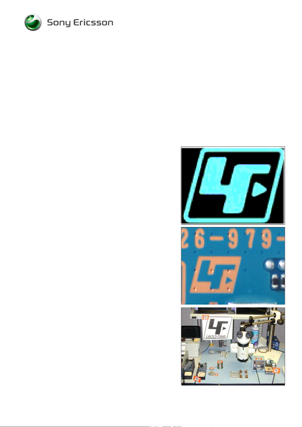
This symbol indicates that the product is lead- free.
All lead-free PBA’s will be marked with this symbol.
A lead-free work area must be set up completely separated from
work areas that are used to make lead repairs.
The lead-free work area must also be clearly labeled with the lead
free symbol as shown in the adjacent picture.
The items on this desk must remain lead-free.
They must be adequately labeled to make their lead-free status
clearly and easily recognized.
3/000 21-2/FEA 209 544/127 B
©
Company Internal
Sony Ericsson Mobile Communications AB
2(16)
Page 3
Working Instruction, Electrical
LFS (lead-free solder paste) characteristics:
High melting point (typically 220°C)
Low wettability
High surface tension
Difficult to spread
Recommended tip temperature = 370°C
W
HEN SERVICING
LFS (
WITH
I
F NOT, THERE IS A HIGH RISK FOR UNRELIABLE SOLDERING
JOINTS
LEAD-FREE SOLDER PASTE),
.
PBA’
S THAT HAVE BEEN MANUFACTURED
LFS
MUST BE USED
.
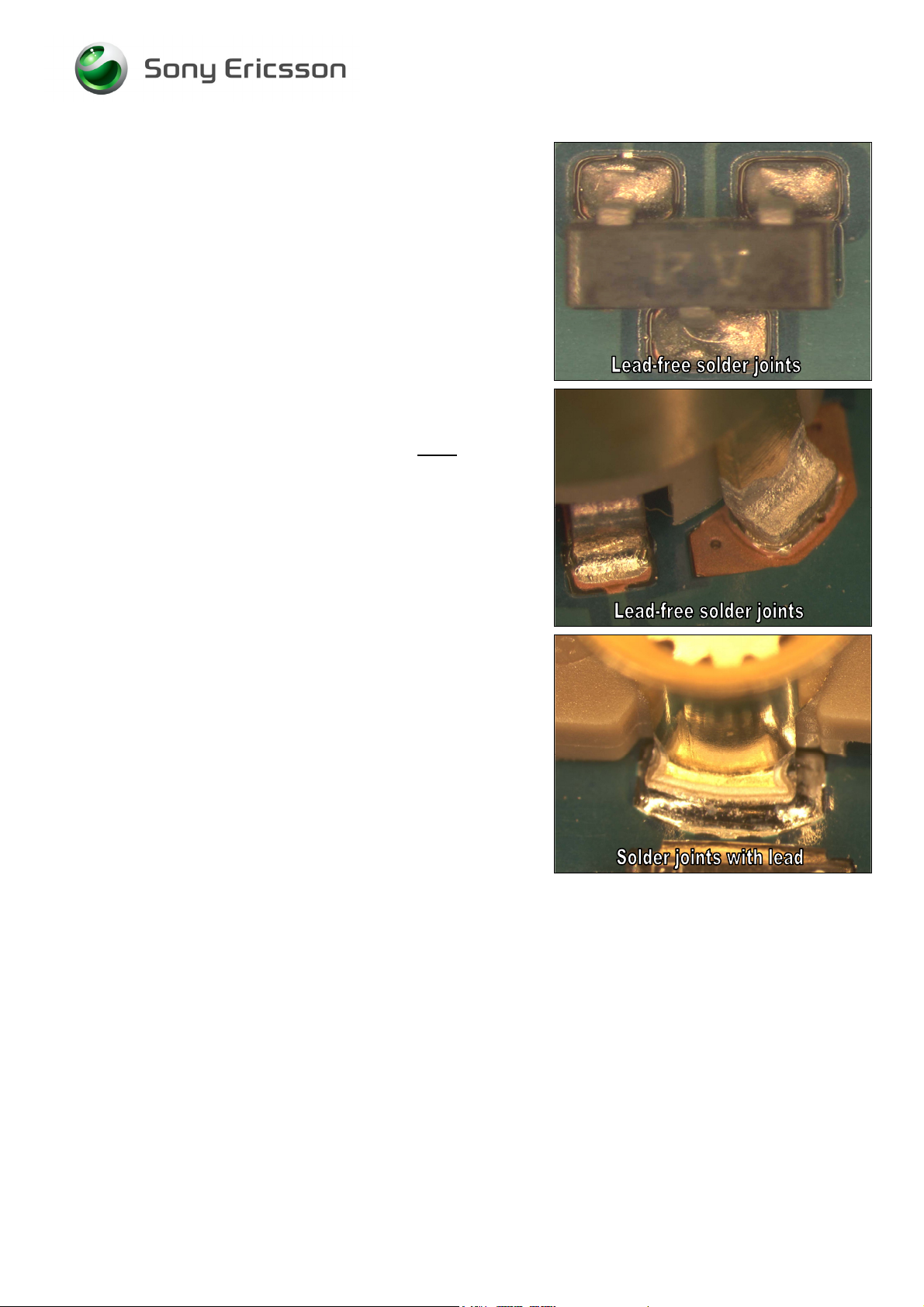
Lead-free solder joints are more difficult to inspect because they
do not have shiny surfaces like leaded solder joints.
Also, lead-free solder does not flow as well as leaded solder, so
some of the solder pad areas may remain exposed.
3/000 21-2/FEA 209 544/127 B
©
Company Internal
Sony Ericsson Mobile Communications AB
3(16)
Page 4

Working Instruction, Electrical
2 BGA equipment reflow profiles
2.1 General
This document contains reflow profile recommendations for mobile phones and similar
products.
They are just general recommendations and considerations have to be taken for every single
product.
The solder paste is secondary but could also affect the parameters.
In this document one alloy is specified:
SnAgCu (Lead free) melting point 217°C
2.2 Temperature measurement
At least two probes should be used. Primary thermocouple should be attached from back side
of the board on a drilled hole under the middle of the component because that is usually the
coolest part of component during reflow. Second thermocouple should be attached on the top
of the component body.
It is recommended that the probes are soldered on the board, but glue and capton tape could
also be used, if necessary.
Nozzle type will be chosen after the outer size of the actual component.
Make sure the nozzle does not affect any nearby placed components.
These values are recommendations and may have to be changed depending on the type of
equipment.
The maximum temperature for any component must not exceed 260
°C.
3/000 21-2/FEA 209 544/127 B
©
Company Internal
Sony Ericsson Mobile Communications AB
4(16)
Page 5
Working Instruction, Electrical
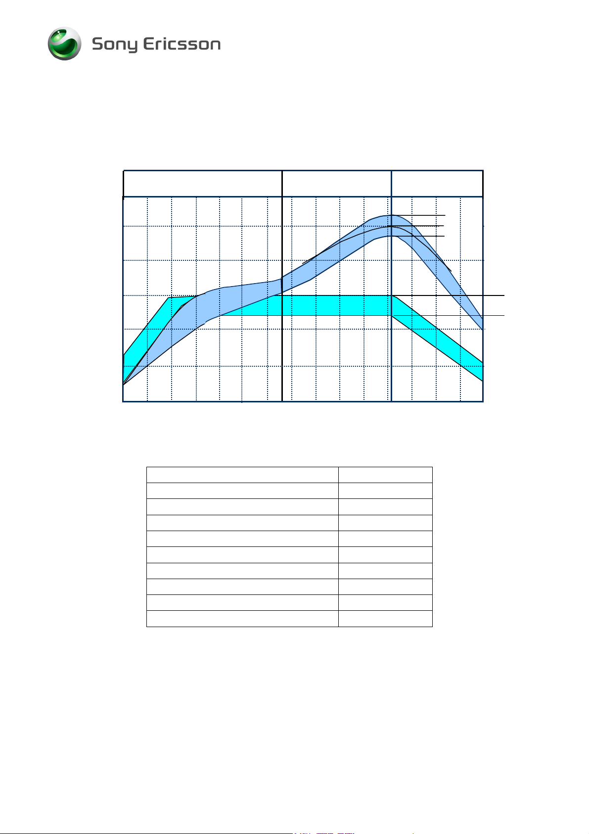
2.3 Reflow profiles
Sn/Ag/Cu (lead-free)
290
250
Reflow zone
260°C
245°C
230°C
200
150
Temperature [ºC]
100
150°C
125°C
50
0
40 80 120 160 200 240 280
Time [Seconds]
Ramp rate < 3°C/sec
Ramp rate cooling < 4°C/sec
Pre heating time 60-150 sec
Time above liquid 40-70 sec
Minimum temperature 230°C
Maximum temperature 245°C°
Maximum component temperature 260 °C
Time between 230 and 245 30 sec
Board temperature bottom side 160°C-185°C
Total time Approx. 3-5min
3/000 21-2/FEA 209 544/127 B
©
Company Internal
Sony Ericsson Mobile Communications AB
5(16)
Page 6

Working Instruction, Electrical
3 Replacement of components
EQUIPMENT
• Dentist hook
• ESD-gloves (cotton gloves)
• ESD-wristband
• Soldering tool
• Hot air soldering station
• Under Heat Equipment
• BGA Station
• Pair of tweezers
• Solder wick
• Solder paste lead-free (SN 96% Ag 3.5% Cu 0.5%)
• Flux, RMA no-clean flux
CAUTION
• Keep all contact surfaces clean of dirt and hand-grease!
• Remove the VGA Camera before starting repairing the board using hot air!
MECHANICAL INSTRUCTIONS
For all the following part replacements, disassemble and assemble the phone as described in
Working Instruction 3/00021-1/FEA 209 544/127.
3/000 21-2/FEA 209 544/127 B
©
Company Internal
Sony Ericsson Mobile Communications AB
6(16)
Page 7

Working Instruction, Electrical
3.1 LED D317: Charge LED Red
Remove the
Use the hot air soldering equipment.
Place the
Use the soldering iron equipment.
LED Red
LED Red
.
.
3.2 D314, D316, D319, D360: Keypad Led Blue
Remove the
Use the hot air soldering equipment.
Place the
Use the soldering iron equipment.
LED Blue
LED Blue
.
.
3/000 21-2/FEA 209 544/127 B
©
Company Internal
Sony Ericsson Mobile Communications AB
7(16)
Page 8

Working Instruction, Electrical
3.3 J308: LCD Display
R
EMOVE THE
Place the PBA in the Fixture
VGA
CAMERA FIRST
Loosen the snaps on the side of the board to release the
LCD Display from the PBA
A PART OF THE FLEXFILM IS ATACHED WITH ADESIVE TO THE
BOARD
BE CAREFULL TO NOT REMOVE THE SOLDERING PADS
Separate the Flex film from board
Lift the LCD Display and cut the Flex film
3/000 21-2/FEA 209 544/127 B
©
Company Internal
Sony Ericsson Mobile Communications AB
8(16)
Page 9

Working Instruction, Electrical
J308: LCD Display continued
Use under heat station to support the soldering process
Use Hot Air Station to remove the rest of Flex film
K
EEP THE UNDER HEAT STATION ON
Add Flux and remove the solder residual
Use Soldering Iron and Solder wick
Clean the pads with alcohol
P
LEASE NOTICE THAT THE SPARE PART
FROM THE ORIGINAL
THE SPARE PART
OF THE FLEX FILM
LCD
HAS SOLDERING PADS ON BOTH SIDES
LCD
IS DIFFERENT
Align the new Flex film with the board pads
Apply flux and solder with Soldering Iron
Start by applying heat on the pads of the board and then
slide the tip on top of the flex film
Clean the pads with alcohol
Use microscope to inspect the repair result
3/000 21-2/FEA 209 544/127 B
©
Company Internal
Sony Ericsson Mobile Communications AB
9(16)
Page 10

Working Instruction, Electrical
3.4 J402: Camera Socket
P
ROTECT THE BATTERY CONNECTOR WITH CAPTON TAPE
R
EMOVE THE
PCB
SPONGE FIRST
Use BGA Station to change the Camera Socket
!
3.5 J602: Antenna Connector
R
EMOVE THE
Use Hot Air Station to remove the Antenna Connector
Use BGA Repair Station to mount the Antenna Connector
PCB
SPONGE FIRST
3/000 21-2/FEA 209 544/127 B
©
Company Internal
Sony Ericsson Mobile Communications AB
10(16)
Page 11

Working Instruction, Electrical
3.6 J302: SIM Connector
Use BGA Station to replace the SIM Connector
3.7 J305: Battery Connector
PROTECT THE CAMERA SOCKET WITH CAPTON TAPE
Use BGA station to replace the Battery Connector
3/000 21-2/FEA 209 544/127 B
©
Company Internal
Sony Ericsson Mobile Communications AB
11(16)
Page 12

Working Instruction, Electrical
3.8 U604: IC Charger
Use BGA Station to replace the IC Charger
3.9 U606: FM Module (K220 Only)
Use BGA Station to replace the FM Module
3/000 21-2/FEA 209 544/127 B
©
Company Internal
Sony Ericsson Mobile Communications AB
12(16)
Page 13

Working Instruction, Electrical
3.10 U702: Audio Power Amplifier (K220 Only)
Use BGA Station to replace the Audio Power Amplifier
3.11 U605: IRDA Module
R
EMOVE THE
Use Hot Air Station to remove the IRDA Module
Use Soldering Iron to replace the IRDA Module
PCB
SPONGE FIRST
3/000 21-2/FEA 209 544/127 B
©
Company Internal
Sony Ericsson Mobile Communications AB
13(16)
Page 14

Working Instruction, Electrical
3.12 U306: Melody IC
Use BGA Station to replace the Melody IC
3.13 U307: IC Charge Pump
Use Hot Air Station to replace the IC Charge Pump
3/000 21-2/FEA 209 544/127 B
©
Company Internal
Sony Ericsson Mobile Communications AB
14(16)
Page 15

Working Instruction, Electrical
3.14 R201: NTC Resistor
P
ROTECT THE BATTERY CONNECTOR WITH CAPTON TAPE
Use Hot Air Station to replace the NTC Resistor
!
3.15 Shield can Lid Assy
D
O NOT REUSE THE SHIELDCAN LID
!
3/000 21-2/FEA 209 544/127 B
©
Company Internal
Sony Ericsson Mobile Communications AB
15(16)
Page 16

Working Instruction, Electrical
4 Revision history
Rev. Date Changes / Comments
A 2007-05-04 First release
B 2007-09-21 New component added, R201 NTC Resistor
3/000 21-2/FEA 209 544/127 B
©
Company Internal
Sony Ericsson Mobile Communications AB
16(16)
 Loading...