

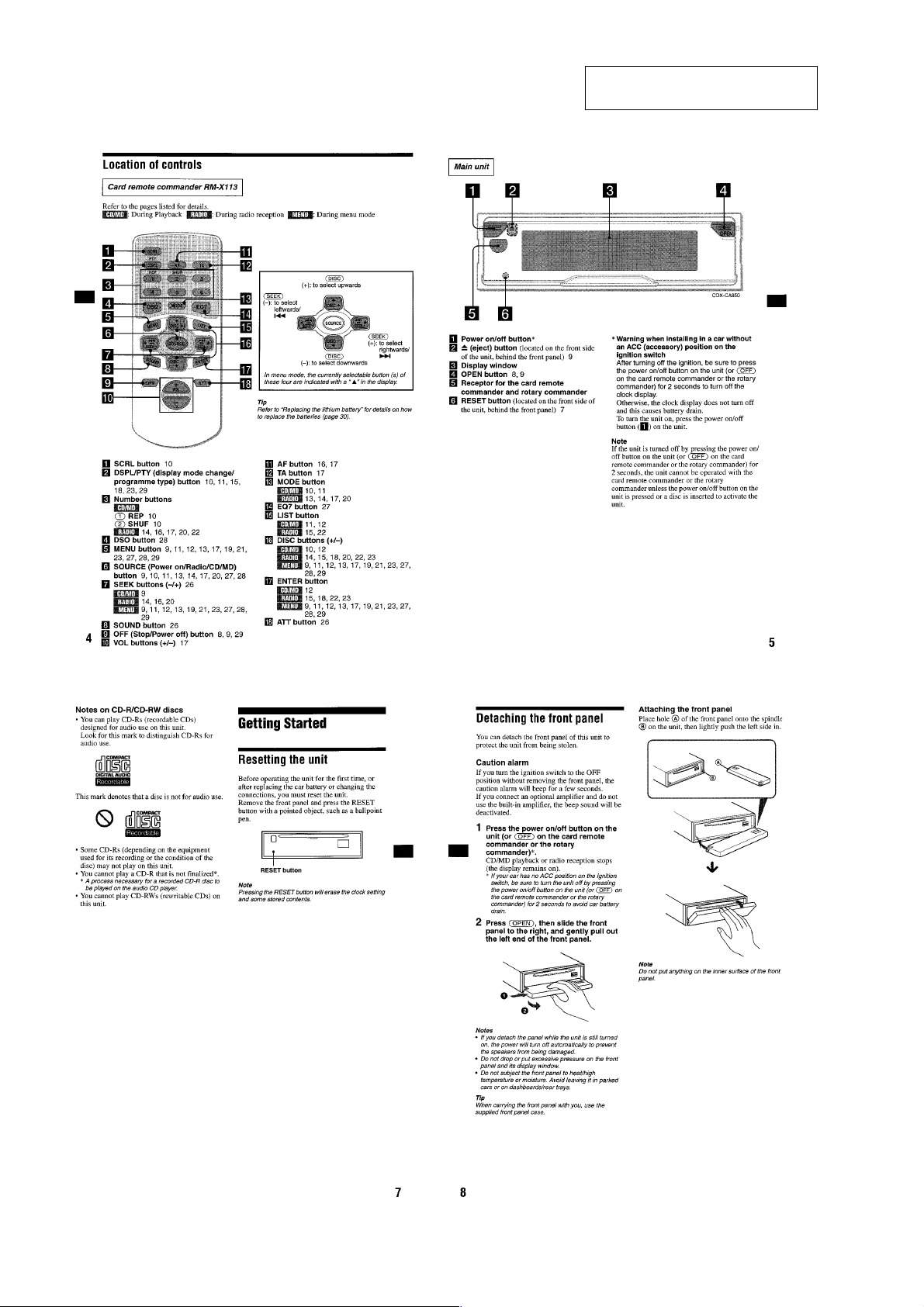
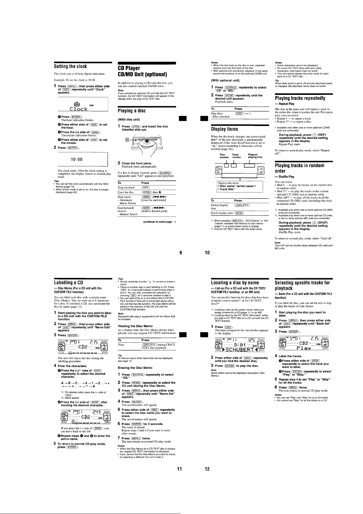
Page 1
CDX-CA850/CA850X/CA860X
SERVICE MANUAL
Ver 1.1 2001. 04
Photo: CDX-CA850X
• The tuner and CD sections have no adjustments.
AUDIO POWER SPECIFICATIONS (US Model)
POWER OUTPUT AND TOTAL HARMONIC DISTORTION
23.2 watts per channel minimum continuous average power into
4 ohms, 4 channels driven from 20 Hz to 20 kHz with no more
than 5% total harmonic distortion.
CD player section
Signal-to-noise ratio 90 dB
Frequency response 10 – 20,000 Hz
Wow and flutter Below measurable limit
Laser Diode Properties (US, Canadian Model)
Material GaAlAs
Wavelength 780 nm
Emission Duration Continuous
Laser output power Less than 44.6 µW*
* This output is the value measured at a distance
of 200 mm from the objective lens surface on the
Optical Pick-up Block.
Tuner section
FM
Tuning range 87.5 – 107.9 MHz (US, Canadian model)
87.5 – 108.0 MHz (AEP, UK model)
Antenna terminal External Antenna connector
Intermediate frequency 10.7 MHz/450 kHz
Usable sensitivity 8 dBf
Selectivity 75 dB at 400 kHz
Signal-to-noise ratio 66 dB (stereo),
72 dB (mono)
Harmonic distortion at 1 kHz
0.6% (stereo),
0.3% (mono)
Separation 35 dB at 1 kHz
Frequency response 30 – 15,000 Hz
AM (US, Canadian model)
Tuning range 530 – 1,710 kHz (US, Canadian model)
Antenna terminal External Antenna connector
Intermediate frequency 10.7 MHz/450 kHz
Sensitivity 30 µV
MW/LW (AEP, UK model)
Tuning range MW: 531 – 1,602 kHz
LW: 153 – 279 kHz
Aerial terminal External Aerial connector
Intermediate frequency 10.7 MHz/450 kHz
Sensitivity MW: 30 µV
LW : 40 µV
SPECIFICATIONS
FM/MW/LW COMPACT DISC PLAYER
US Model
Canadian Model
CDX-CA850X/CA860X
AEP Model
UK Model
CDX-CA850
Model Name Using Similar Mechanism CDX-C5000R
CD Drive Mechanism Type MG-383Z-121//Q
Optical Pick-up Name KSS-720A
Power amplifier section
Outputs Speaker outputs
(sure seal connectors)
Speaker impedance 4 – 8 ohms
Maximum power output 52 W × 4 (at 4 ohms)
General
Outputs Audio outputs (front/rear)
Subwoofer output (mono)
Power Antenna relay control lead
Power amplifier control lead
Inputs Telephone ATT control lead
Illumination control lead
Bus control input connector
Bus audio input connector
Remote controller input connector
Antenna input connector
Tone controls Bass ±10 dB at 62 Hz (US, Canadian model)
Bass ±8 dB at 100 Hz (AEP, UK model)
Treble ±10 dB at 16 kHz (US, Canadian model)
Treble ±8 dB at 10 kHz (AEP, UK model)
Loudness +8 dB at 100 Hz
+2 dB at 10 kHz
Power requirements 12 V DC car battery
(negative ground)
– Continued on next page –
CDX-CA850
FM/AM COMPACT DISC PLAYER
CDX-CA850X/CA860X
9-870-291-12
2001D0400-1
© 2001. 4
Sony Corporation
e Vehicle Company
Shinagawa Tec Service Manual Production Group
1
Page 2
CDX-CA850/CA850X/CA860X
k
Dimensions Approx. 178 × 50 × 177 mm
(7 1/8 × 2 × 7 in.) (w/h/d)
Mounting dimensions Approx. 182 × 53 × 162 mm
(7 1/4 × 2 1/8 × 6 1/2 in.) (w/h/d)
Mass Approx. 1.3 kg
(2 lb. 10 oz.)
Supplied accessories Parts for installation and connections (1 set)
Front panel case (1)
Rotary commander
RM-X5S
Card remote commander
RM-X112 (CDX-CA850X/CA860X)
RM-X113 (CDX-CA850)
Note
This unit cannot be connected to a digital preamplifier or an equalizer.
Design and specifications are subject to change without
notice.
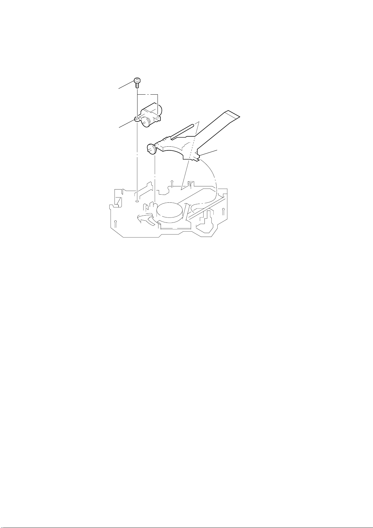
SERVICE NOTES
• US, Canadian model
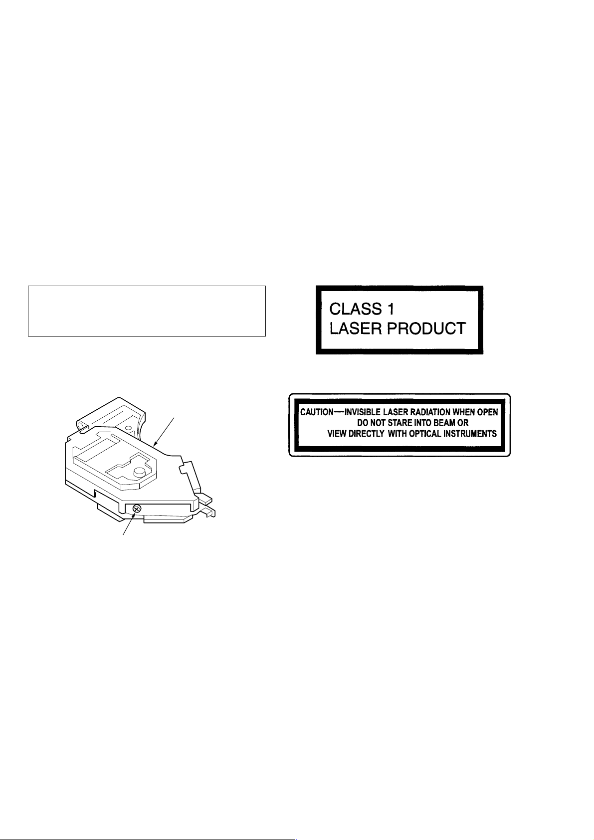
CAUTION
Use of controls or adjustments or performance of procedures
other than those specified herein may result in hazardous
radiation exposure.
If the optical pick-up block is defective, please replace the whole
optical pick-up block.
Never turn the semi-fixed resistor located at the side of optical
pick-up block.
• AEP, UK model
This label is located on the bottom of the chassis.
optical pick-up bloc
semi-fixed resistor
NOTES ON HANDLING THE OPTICAL PICK-UP BLOCK
OR BASE UNIT
The laser diode in the optical pick-up block may suffer electrostatic
breakdown because of the potential difference generated by the
charged electrostatic load, etc. on clothing and the human body.
During repair, pay attention to electrostatic breakdown and also use
the procedure in the printed matter which is included in the repair
parts.
The flexible board is easily damaged and should be handled with
care.
This label is located on the drive unit's internal
chassis.
When replacing the chassis (T .U) of mechanism deck which have
the “CAUTION LABEL” attached, please be sure to put a new
CAUTION LABEL (3-223-913-11) to the chassis (T.U).
NOTES ON LASER DIODE EMISSION CHECK
The laser beam on this model is concentrated so as to be focused on
the disc reflective surface by the objective lens in the optical pickup block. Therefore, when checking the laser diode emission, observe from more than 30 cm away from the objective lens.
Notes on Chip Component Replacement
• Never reuse a disconnected chip component.
• Notice that the minus side of a tantalum capacitor may be dam-
aged by heat.
SAFETY-RELATED COMPONENT WARNING!!
COMPONENTS IDENTIFIED BY MARK 0 OR DOTTED LINE
WITH MARK 0 ON THE SCHEMATIC DIAGRAMS AND IN
THE PARTS LIST ARE CRITICAL TO SAFE OPERATION.
REPLACE THESE COMPONENTS WITH SONY P ARTS WHOSE
PART NUMBERS APPEAR AS SHOWN IN THIS MANUAL OR
IN SUPPLEMENTS PUBLISHED BY SONY.
2
ATTENTION AU COMPOSANT AYANT RAPPORT
À LA SÉCURITÉ!!
LES COMPOSANTS IDENTIFIÉS P AR UNE MARQUE 0 SUR LES
DIAGRAMMES SCHÉMATIQUES ET LA LISTE DES PIÈCES
SONT CRITIQUES POUR LA SÉCURITÉ DE FONCTIONNEMENT.
NE REMPLACER CES COMPOSANTS QUE PAR DES PIÈCES
SONY DONT LES NUMÉROS SONT DONNÉS DANS CE MANUEL
OU DANS LES SUPPLÉMENTS PUBLIÉS PAR SONY.
Page 3

TABLE OF CONTENTS
CDX-CA850/CA850X/CA860X
Ver 1.1 2001. 04
1. GENERAL
........................................................................... 4
2. DISASSEMBLY
2-1. Sub Panel Assy.................................................................. 10
2-2. CD Mechanism Block ....................................................... 10
2-3. Main Board ....................................................................... 10
2-4. Heat Sink ........................................................................... 11
2-5. Chassis (T) Assy................................................................ 11
2-6. Lever Section..................................................................... 12
2-7. Servo Board....................................................................... 12
2-8. Arm Roller Assy................................................................ 13
2-9. Chassis (OP) Assy............................................................. 13
2-10. Optical Pick-up Block ....................................................... 14
3. DIAGRAMS
3-1. IC Pin Descriptions ........................................................... 15
3-2. Block Diagram –CD Section–........................................... 23
3-3. Block Diagram –Tuner Section–....................................... 24
3-4. Block Diagram –Display Section–.................................... 25
3-5. Circuit Boards Location .................................................... 26
3-6. Printed Wiring Boards –CD Mechanism Section–............ 28
3-7. Schematic Diagram –CD Mechanism Section (1/2)– ....... 30
3-8. Schematic Diagram –CD Mechanism Section (2/2)– ....... 31
3-9. Printed Wiring Boards –Main Section– ............................ 32
3-10. Schematic Diagram –Main Section (1/4)– ........................ 34
3-11. Schematic Diagram –Main Section (2/4)– ........................ 35
3-12. Schematic Diagram –Main Section (3/4)– ........................ 36
3-13. Schematic Diagram –Main Section (4/4)– ........................ 37
3-14. Printed Wiring Board –Sub (CD) Section–....................... 38
3-15. Schematic Diagram –Sub (CD) Section–.......................... 39
3-16. Printed Wiring Board –Key Section–................................ 40
3-17. Schematic Diagram –Key Section–................................... 41
4. EXPLODED VIEWS
4-1. Chassis Section ................................................................. 46
4-2. Front panel Section ........................................................... 47
4-3. CD Mechanism Section (1) ............................................... 48
4-4. CD Mechanism Section (2) ............................................... 49
4-5. CD Mechanism Section (3) ............................................... 50
5. ELECTRICAL PARTS LIST ........................................ 51
3
Page 4
CDX-CA850/CA850X/CA860X
SECTION 1
GENERAL
This section is extracted from AEP,
UK model’s instruction manual.
4
Page 5
CDX-CA850/CA850X/CA860X
5
Page 6
CDX-CA850/CA850X/CA860X
6
Page 7
CDX-CA850/CA850X/CA860X
7
Page 8
CDX-CA850/CA850X/CA860X
8
Page 9
Connection
CDX-CA850/CA850X/CA860X
99
Page 10
CDX-CA850/CA850X/CA860X
4
4
SECTION 2
DISASSEMBLY
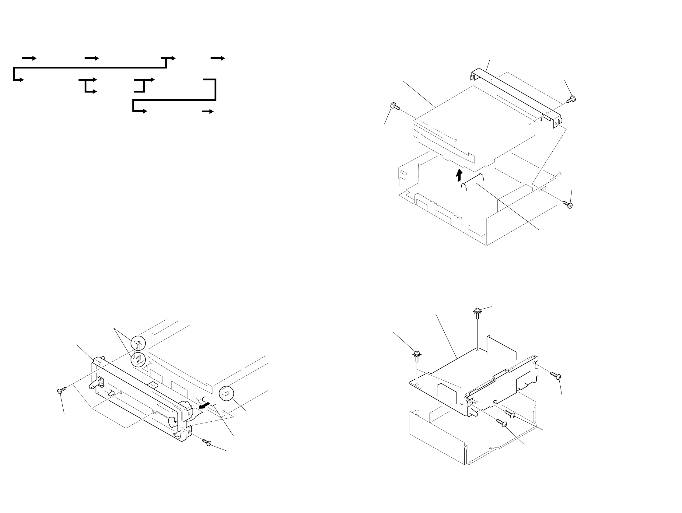
Note : This equipment can be removed using the following procedure.
Set Sub Panel Assy CD Mechanism Block
Chassis (T) Assy lever Section
Servo Board
Chassis (OP) Assy Optical Pick-up Block
Main Board Heat Sink
Arm Roller Assy
2-2. CD MECHANISM BLOCK
5 CD mechanism block
2 PTT 2.6x4
7 bracket (CD)
6 PTT 2.6x4
3
1 PTT 2.6x
Note : Follow the disassembly procedure in the numerical order given.
2-1. SUB PANEL ASSY
4 two claws
6 sub panel assy
2-3. MAIN BOARD
6 MAIN board
5 ground point screws
(PTT 2.6x6)
4 CN401
4 ground point screw
(PTT 2.6x6)
3 PTT 2.6x
2 PTT 2.6x6
3 claw
2 PTT 2.6x4
5 CN701
1 PTT 2.6x6
1 PTT 2.6x4
1010
Page 11
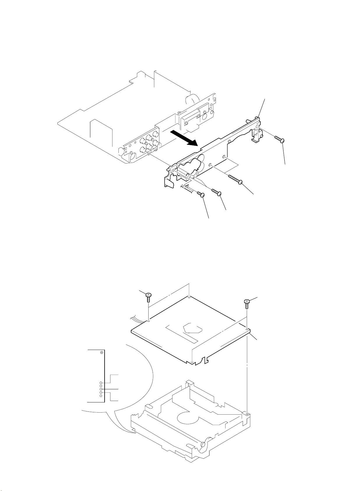
0
2-4. HEAT SINK
CDX-CA850/CA850X/CA860X
5 heat sink
3 PTT 2.6x1
2-5. CHASSIS (T) ASSY
1 Unsolder the
lead wires.
2 PTT 2.6x16
1 PTT 2.6x10
4 PTT 2.6x4
2 P 2x3
3 P 2x3
4 chassis (T) assy
black
red
white
11
Page 12
CDX-CA850/CA850X/CA860X
2-6. LEVER SECTION
5
6
lever (R) sub assy
3
tension spring (LR)
7
lever (L) sub assy
guide (disc)
1
PS 2x4
2
DISC IN board
2-7. SERVO BOARD
8 loading motor assy
(M903)
4
claws
9 PS 2x4
5 Removal the solders.
3 CN3
7 P 2x3
1 PS 2x5
2 heat sink (CD)
7 PS 2x4
4 CN2
0 SERVO board
6 Removal the solders.
12
Page 13
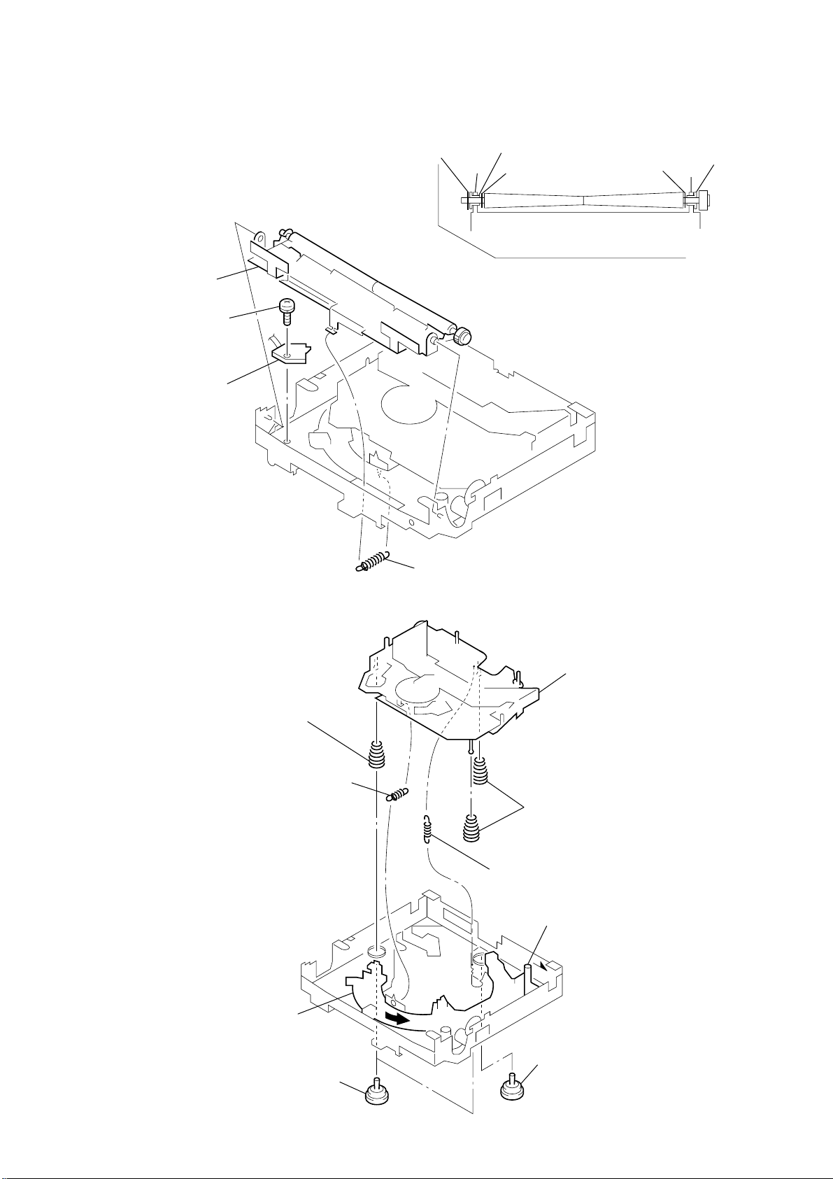
3 PS 2x3
4 LOAD board
1 tension spring (RA2)
2 arm roller assy
Fig. 1
retaining ring (roller)
arm
arm
washer(RA)
washer(RA)
bearing (roller)
bearing (roller)
2-8. ARM ROLLER ASSY
• When installing, take note of the positions
arm (roller) and washers. (Fig. 1)
CDX-CA850/CA850X/CA860X
2-9. CHASSIS (OP) ASSY
8 compression spring (FL)
1 tension spring (KF1)
9 compression spring (FL)
2 tension spring (KR1)
7 chassis (OP) assy
5 Fit lever (D) in the
direction of the arrow.
6 Turn loading ring in the
direction of the arrow.
4 damper (T)
3 damper (T)
13
Page 14
CDX-CA850/CA850X/CA860X
2-10. OPTICAL PICK-UP BLOCK
1 P 2x3
2 sled motor assy
(M902)
3 optical pick-up block
14
Page 15

CDX-CA850/CA850X/CA860X
SECTION 3
DIAGRAMS
3-1. IC PIN DESCRIPTIONS
• IC501 CXD2598Q (DIGITAL SER VO, DIGITAL SIGNAL PROCESSOR) (SER VO BOARD)
Pin No. Pin Name I/O Pin Description
1 DVDD — Digital power supply pin
2 DVSS — Digital ground
3 SOUT O Servo brock serial data output (Not used.)
4 SOCK O Servo brock serial data read clock output (Not used.)
5 XOLT O Servo brock serial data latch output (Not used.)
6 SQSO O Sub Q 80 bit, PCM peak and level data output. CD TEXT data output
7 SQCK I Clock input from SQSO read output.
8 SCSY I Fixed at “L”.
9 SBSO O Serial output of sub-P to W. (Not used.)
10 EXCK I Clock input from SBSO read output. (Fixed at “L”)
11 XRST I System reset (“L”: Reset)
12 STSM I System mute input (Fixed at “L”)
13 DATA I Serial data input from CPU.
14 XLAT I Latch input from CPU. Latch serial data at the falling edge.
15 CLOK I Serial data transfer clock input from CPU.
16 SENS O SENS output for CPU.
17 SCLK I Clock input from SENS serial data read.
18 ATSK I/O Input/output for anti-shock.
19 WFCK O WFCK (Write Flame Clock) output (Not used.)
20 XUGF O XUGF output (Not used.)
21 XPCK O XPCK output (Not used.)
22 GFS O GFS output
23 C2PO O C2PO output (Not used.)
24 SCOR O “H” output at either detection, sub code sync S0 or S1.
25 C4M O 4.2336 MHz output (Not used.)
26 WDCK O Word clock input f=2Fs (Not used.)
27 COUT I/O Track number count signal input/output (Not used.)
28 MIRR I/O Mirror signal input/output (Not used.)
29 DVSS — Digital ground
30 DVDD — Digital power supply pin
31 DFCT I/O Diffect signal input/output (Not used.)
32 FOK I/O Focus OK signal output
33 PWM1 I External control input of spindle motor.
34 LOCK I/O Lock signal input/output
35 MDP O Servo control output of spindle motor.
36 SSTP I Disc most inner track detection signal input
37 FSTIO I/O 2/3 frequency division output of pins ih and ij. (Not used.)
38 SFDR O Sled drive output
39 SRDR O Sled drive output
40 TFDR O Tracking drive output
41 TRDR O Tracking drive output
42 FFDR O Focus drive output
43 FRDR O Focus drive output
44 DVDD — Digital power supply pin
45 DVSS — Digital ground
46 TEST I Test pin (Fixed at “L”)
47 TES1 I Test pin (Fixed at “L”)
48 XTSL I X’tal select input (“L”: 16.9344 MHz, “H”: 33.8688 MHz)
49 VC I Center voltage input
50 FE I Focus error signal input
51 SE I Sled error signal input
15
Page 16

CDX-CA850/CA850X/CA860X
Pin No. Pin Name I/O Pin Description
52 TE I Tracking error signal input
53 CE I Center servo analog input
54 RFDC I RF signal input
55 ADIO O Test pin (Not used.)
56 AVSSO — Analog ground
57 IGEN I Constant current input from OP amplifier.
58 AVDDO — Analog ground
59 ASYO O EFM full-swing output (“L”: VSS, “H”: VDD)
60 ASYI I Asymmetry comparate voltage input
61 RFAC I EFM signal input
62 AVSS3 — Analog ground
63 CLTV I VCO control voltage input from master.
64 FILO O Filter output for master PLL (slave=digital PLL)
65 FILI I Filter input from master PLL.
66 PCO O Charge pump output for master PLL.
67 AVDD3 — Analog power supply pin
68 BIAS I Asymmetry circuit constant current input
69 VCTL I VCO2 control input from wideband EFM PLL. (Not used.)
70 V16M O VCO2 oscillator output for wideband EFM PLL. (Not used.)
71 VPCO O Charge pump output for wideband EFM PLL. (Not used.)
72 DVSS — Digital ground
73 MD2 I Digital out ON/OFF control input (“L”: OFF, “H”: ON)
74 DOUT O Digital out output
75 ASYE I Asymmetry circuit ON/OFF input (“L”: OFF, “H”: ON)
76 DVDD — Digital power supply pin
77 LRCK O D/A interface LR clock output (f=Fs)
78 LRCKI I D/A interface LR clock input
79 PCMD O D/A interface serial data output (2’s COMP, MSB fast)
80 PCMDI I D/A interface serial data input (2’s COMP, MSB fast)
81 BCK O D/A interface bit clock output
82 BCKI I D/A interface bit clock input
83 EMPH O Emphasis ON/OFF signal output
84 EMPHI I Emphasis ON/OFF signal input (“H”: ON, “L”: OFF)
85 XVDD — Power supply for master clock.
86 XTAI I X’tal oscillator input from master clock (16.9344 MHz).
87 XTAO O X’tal oscillator output for master clock (16.9344 MHz).
88 XVSS — Ground pin for master clock.
89 AVDD1 — Analog power supply pin
90 AOUT1 O Lch analog output
91 AIN1 I Lch OPAMP input
92 LOUT1 O Lch LINE output
93 AVSS1 — Analog ground
94 AVSS2 — Analog ground
95 LOUT2 O Rch LINE output
96 AIN2 I Rch OPAMP input
97 AOUT2 O Rch analog output
98 AVDD2 — Analog power supply pin
99 RMUT O Rch “0” detect Flug (Not used.)
100 LMUT O Lch “0” detect Flug (Not used.)
16
Page 17
CDX-CA850/CA850X/CA860X
• IC5 CXP84640-072Q (CD SYSTEM CONTROL) (SERVO BOARD)
Pin No. Pin Name I/O Pin Description
1 ITRPT — Not used in this set.
2, 3 — — Not used in this set.
4, 5 NCO — Not used in this set.
6 OPEN I Front panel open detection input
7 CLOSE O Front panel close control output
8 LINKOFF I Bus interface link input
9 NCO — Not used in this set.
10 D SW I Down switch input (SW4)
11 SSTP I Limit switch input (SW3)
12, 13 NCO — Not used in this set.
14, 15 — — Not used in this set.
16 EMPH O O De-emphasis ON/OFF control output
17 CDMON O CD mechanism deck power control output
18 CD ON O CD power control output
19 A MUT O System attenuate control output
20 LD ON O Laser power ON/OFF control output
21 CD RST O CD system reset output
22 HOLD O Hold switch output
23 AGC CONT O AGC control output
24 — — Not used in this set.
25 PH3 I Not used in this set.
26 TSTIN0 I Not used in this set.
27 TSTIN1 I Not used in this set.
28 TST.CLV I Not used in this set.
29 NCO — Not used in this set.
30 RESET I System reset input (“L”=Reset)
31 X IN I X’tal oscillator input from system clock. (10 MHz)
32 X OUT O X’tal oscillator output for system clock. (10 MHz)
33 GND — Analog ground
34 XT OUT O Not used in this set.
35 XT IN I Not used in this set.
36 AVSS — A/D converter ground
37 AVREF I A/D converter reference voltage input
38 TEP L I Not used in this set.
39 TEP H I Not used in this set.
40 SLED– I Sled drive input
41 PH2 I Not used in this set.
42 SEK/SMET I Fixed at “H” in this set.
43 GFS/MNT2 SEL I Fixed at “H” in this set.
44 SC-JIG ON/OFF I Fixed at “H” in this set.
45 SCLK O CD-TEXT data read clock output
46 LOCK I/O Lock signal input/output
47 — — Not used in this set.
48 SCK2 O Sub Q read clock output
49 SI2 I Sub Q 80 bit, PCM peak and level data 16 bit input.
50 — — Not used in this set.
51 BUS CLK I/O Bus system serial clock input/output
52 BUS SI I Bus system serial interface input
53 BUS SO O Bus system serial interface output
54 F OK I Focus OK signal input
55 GFS I GFS signal detection input
56 TEST MODE I Fixed at “H” in this set.
17
Page 18
CDX-CA850/CA850X/CA860X
Pin No. Pin Name I/O Pin Description
57 SENS I SENS signal input
58 — — Not used in this set.
59 — — Not used in this set.
60 BU.IN I Back-up power detection input
61 BUSON I Bus on control input
62 IN SW I Disc in switch input (SW1)
63 SELF SW I Self switch input (SW2)
64 SCOR O Sub-code sync output
65 CD-CKO O CD signal process serial clock input
66 LM LOD O Loading motor control output
67 CD DATA O CD signal process serial data output
68 CD-XLAT O CD signal process serial data latch output
69 LM-EJ O Loading motor control output
70 DRV-OE O Focus/tracking coil/sled motor control output
71 MD2 O Digital out ON/OFF control output (“L”: OFF, “H”: ON)
72 VDD — Power supply pin
73 NIH I Fixed at “H” in this set.
74 V/Z I Fixed at “H” in this set.
75 PH1 I Not used in this set.
76 — — Not used in this set.
77 DOUT-SEL I Fixed at “H” in this set.
78 – 80 — — Not used in this set.
18
Page 19
CDX-CA850/CA850X/CA860X
• IC501 MB90574BPMT-G-323-BND (MAIN SYSTEM CONTROL) (CDX-CA850X/CA860X) (MAIN BOARD)
• IC501 MB90574BPMT-G-324-BND (MAIN SYSTEM CONTROL) (CDX-CA850) (MAIN BOARD)
Pin No. Pin Name I/O Pin Description
1 – 4 NCO O Not used. (Open)
5 ATT O System mute control signal output
6, 7 NCO O Not used. (Open)
8 VCC — Power supply pin (+5 V)
9 AMP ATT O Amp mute signal output
10 E2PSIO I/O EEPROM data signal input/output
11 E2PCKO O EEPROM clock signal output
12 DOOR SW/FLS SI I Door switch signal input (L: close) Flash write data signal input
13 FLS SO O Flash write data signal output
14 BUS ON O BUS ON control signal output
15 BEEP O Beep signal output
16 NS MASK O Tuner mute signal output
17 UNISI I SONY BUS data signal input
18 UNISO O SONY BUS data signal output
19 UNICKO O SONY BUS clock signal output
20 IFWIDTH O Not used. (Open)
21 SWSHIFT O Not used. (Open)
22 SYSRST O System reset signal output
23 (NCO) O Not used. (Open)
24 SIRCS I Remote control data signal input
25 – 29 NCO O Not used. (open)
30 AMPON O Amp on signal output (L: OFF/H: ON)
31 VOLATT O Electronic volume mute signal output (L: Mute on)
32 NCO O Not used. (Open)
33 VSS — Ground pin
34 C — Power stabilized capacitance pin Not used. (open)
35 – 37 NCO O Not used. (Open)
38 DVCC — D/A converter VREF input
39 DVSS — D/A converter GND pin
40, 41 (NCO) O Not used. (Open)
42 AVCC — Analog power supply pin (+5 V)
43 AVRH — A/D converter VREF+ input
44 AVRL — A/D converter VREF– input
45 AVSS — Analog ground pin
46 KEYIN0 I Key signal input 0
47 KEYIN1 I Key signal input 1
48 RCIN0 I Rotary commander signal input
49 NCO O Not used. (Open)
50 QUALITY O Quality signal output
51 FM AGC O Not used in this set. (Open)
52 MPTH O MPTH signal output to RDS decoder
53 VSM I S-meter signal input
54 VCC — Power supply pin (+5 V)
55, 56 NCO O Not used. (Open)
57 BOOT O Display microcomputer write control signal output
58 DOORIND O Front panel indicator signal output
59 – 62 NIL I Not used. (Connect to ground in this set.)
63 VSS — Ground pin
64 NIL I Not used. (Connect to ground in this set.)
65 FSW IN O Not used. (Open)
66 – 68 NCO O Not used. (Open)
19
Page 20

CDX-CA850/CA850X/CA860X
Pin No. Pin Name I/O Pin Description
69 FLASH W I Flash write mode detection signal input
70 I2CSIO O Tuner, electronic volume communication data signal output
71 I2CCKO O Tuner, electronic volume communication clock signal output
72 NCO O Not used. (Open)
73 X1A I Low speed oscillation signal input (32.768 kHz)
74 X0A I Low speed oscillation signal input (32.768 kHz)
75 DAVN O DAVN signal output to RDS decoder
76 DISCON IN O Not used. (Open)
77 BUIN I Backup power supply detection signal input
78 NCO O Not used. (Open)
79 KEYACK I KEY ACK detection signal input
80 ADON O A/D conversion power control signal output
81 NOSESW I Front panel attachment detection signal input
82 FLASH ON O Flash write jig power supply output
83 PWON O System power supply control signal output
84 NCO O Not used. (Open)
85 RAMBU I RAM reset detection signal input
86 HSTX I Hardware standby signal input
87 MD2 I Operation mode input (Connect to ground.)
88, 89 MD1, 0 I Operation mode input (Connect to VCC.)
90 RESET I Microcomputer reset signal input
91 VSS — Ground pin
92 X0 I High speed oscillation signal input (3.68 MHz)
93 X1 I High speed oscillation signal input (3.68 MHz)
94 VCC — Power supply pin (+5 V)
95, 96 REIN0, 1 I Rotary encoder signal input
97 – 99 NCO O Not used. (Open)
100 4V SEL X/O I 4 V/5.5 V preout menu with/without initial setting input
101 COLORSEL X/O I Illumination select with/without initial setting input Not used. (Open)
102 MODELSEL0 U/J I Destination setting input Not used. (Open)
103 DOT/L-CUBE I DOT/L-CUBE judgment initial setting input
104 CD/MD I CDX/MDX judgment initial setting input Not used. (Open)
105, 106 NCO O Not used. (Open)
107 RCIN1 (PULL UP) I Rotary commander signal input
108 TESTIN (PULL UP) I Test mode setting detection input
109 TELATT I TEL mute detection signal input
110 ILLIN I Illumination line detection signal input
111, 112 NCO O Not used. (Open)
113 TUNON O Tuner on signal output
114, 115 NCO O Not used. (Open)
116 EMPH O Not used. (Open)
117 ACCIN I ACC power supply detection signal input L: ACC ON
118 NCO O Not used. (Open)
119 VSS — Ground pin
120 NCO O Not used. (Open)
20
Page 21

CDX-CA850/CA850X/CA860X
• IC701 HD6432355A35F (SUB SYSTEM CONTROL)
Pin No. Pin Name I/O Pin Description
1 PG3 O Spectrum analyzer clock output
2 PG4 O Not used (open)
3 VSS — Ground pin
4 NC — Not used (open)
5 VCC — Power supply pin
6 – 9 PC0 – PC3 O Not used (open)
10 VSS — Ground pin
11 – 14 PC4 – PC7 O Not used (open)
15 – 18 PB0 – PB3 O Not used (open)
19 VSS — Ground pin
20 – 23 PB4 – PB7 O Not used (open)
24 – 27 PA0 – PA3 O Not used (open)
28 VSS — Ground pin
29 – 32 PA4 – PA7 O Not used (open)
33 SP LAT(PWON) I Spectrum analyzer latch input
34 BU IN I Back-up power detection input
35 VSS — Ground pin
36 VSS — Ground pin
37 P65 O Not used (open)
38 BUS ON I Bus on control signal
39 VCC — Power supply pin
40 – 43 PE0 – PE3 O Not used (open)
44 VSS — Ground pin
45 – 48 PE4 – PE7 O Not used (open)
49 PD0 O Not used (open)
50 LINK OFF O Bus interface link off control signal
51 PD2 O Not used (open)
52 ILL-ON O Illumination on/off switch signal output
53 VSS — Ground pin
54 – 56 PD4 – PD6 O Not used (open)
57 BOOT I Flash write-in mode detection input
58 VCC — Power supply pin
59 NC — Not used (open)
60 TX/LCD DATA O Flash write-in data/LCD driver data output
61 SP SI O Not used (open)
62 RX I Flash write-in data input
63 L RST O Reset signal for SIRCS inveter
64 LCD SCK O LCD driver clock output
65 VSS — Ground pin
66 LCD CE1 O LCD driver chip enable output
67 VSS — Ground pin
68 VSS — Ground pin
69 LCD INH1 O Not used (open)
70 LCD CE2 O Not used (open)
71 LCD INH2 O Not used (open)
72 – 78 P27 – P21 O Not used (open)
79 P20 O Flash write-in control signal
80 FWE L I Flash write-in enable input
81 RES I Reset signal
82 NMI I Non maskable interrupt signal
83 STBY Standby mode signal
84 VCC — Power supply pin
21
Page 22

CDX-CA850/CA850X/CA860X
Pin No. Pin Name I/O Pin Description
85 XTAL — Crystal oscillator (18.432 MHz)
86 EXTAL — Crystal oscillator (18.432 MHz)
87 VSS — Ground pin
88 PF7 O Not used (open)
89 VCC — Power supply pin
90 – 96 PF6 – PF0 O Not used (open)
97 UNI SO O SONY Bus data output
98 UNI SI I SONY Bus data input
99 VSS — Ground pin
100 VSS — Ground pin
101 UNI SCK I SONY Bus clock input
102 P53 O Not used (open)
103 AVCC — Power supply pin for A/D converter
104 VREF — Reference voltage for A/D converter
105 – 111 P42 – P46 O Not used (Connecting to ground.)
112 P47(SA DATA) I Spectrum analyzer data input
113 AVSS — Ground pin
114 VSS — Ground pin
115 – 122 P17 – P10 O Not used (open)
123 MD0 — Mode select
124 MD1 — Mode select
125 MD2 — Mode select
126 – 128 PG0 – PG2 O Not used (open)
22
Page 23

3-2. BLOCK DIAGRAM — CD SECTION —
CDX-CA850/CA850X/CA860X
OPTICAL PICK-UP
KSS-720A
A
C
B
D
PD
LD
TRACKING
E
F
FOCUS
COIL
COIL
CONV.
I-V
M902
SLED
MOTOR
M901
SPINDLE
MOTOR
M903
LOADING
MOTOR
A
5
C
7
B
6
D
8
FOCUS
ERROR
E
11
TRACKING
F
ERROR
10
PD
4
LD
LD
DRIVE
Q101
TRACKING/FOCUS COIL DRIVE
SLED/SPINDLE/LOADING MOTOR DRIVE
10
11
12
13
AMP
LD
3
IC7
FOCUS
COIL
DRIVE
TRACKING
8
COIL
DRIVE
9
SLED
6
MOTOR
7
DRIVE
SPINDLE
MOTOR
DRIVE
LOADING
5
MOTOR
4
DRIVE
RF AMP, LD APC,
ERROR AMP
IC1
22
21
25
24
31
32
18
1
2
MUTE 1
34
MUTE 2
35
RFO RFAC
RF
EQ
FE
TE
LD ON
HOLD SW
AGC CONT
16
14
13
22
21
20
DIGITAL SERVO,
DIGITAL SIGNAL PROCESSOR
IC501
SUB
D/A
CONV.
LOUT1
LOUT2
LOCK
SQSO
SQCK
SCOR
MD2
XRST
DATA
XLAT
SCLK
CLOK
SENS
GFS
FOK
RFDC
FE
TE
SE
FFDR
FRDR
TFDR
TRDR
SFDR
SRDR
MDP
EFM
DEM
SERVO
CTL
61
54
50
52
51
42
43
40
41
38
39
35
D/A
I/F
DIGITAL
CLV
CODE
PROCESS
92
95
34
6
7
24
73
11
13
14
17
15
16
22
32
(Page 24)
TUNER
SECTION
SW3
(LIMIT)
SW1
(DISC IN)
SW4
(DOWN)
SW2
(SELF)
1
CD L
R-CH
(KEY BOARD)
X1
10MHz
CD SYSTEM CONTROL
IC5
BUS CLK
LOCK
46
OPEN
6
SI2
49
SCK2
48
SCOR
64
MD2
71
CD RST
21
CD DATA
67
CD XLAT
68
SCLK
45
CD CKO
65
SENS
57
GFS
55
FOK
54
31
XIN
32
XOUT
SSTP
11
IN SW
62
D SW
10
SELF SW
63
LM EJ
69
LM LOD
66
SLED –
40
DRIVE OE
70
LD ON
20
HOLD
22
AGC CONT
23
A MUT
CDMON
CDON
BUS SI
BUS ON
RESET
BU IN
BUS SO
TUNER
ATT
SECTION
(Page 24)
19
17
MDON
CDON
18
51
52
61
30
60
53
5
DISPLAY
SECTION
(Page 25)
S101
RESET
SYSTEM CONTROL
IC501 (1/3)
ATT
5
UNI CKO
19
UNI SI
17
UNI SO
18
BUS ON
14
SYS RST
22
BU IN
77
SIRCS
RESET
90
HSTX
86
IC502
1 2
RESET
BUS INTERFACE
IC601
BATT (L)
10 3
CHECK
13 2
RESET
BUS ON
12
CONT
9
8
11
DATA
CLK
• Signal path
:CD
Q603
SIRCS
BUFFER
IC903
BATT
BU DET
Q602
6
5
4
CN601
BUS
CONTROL IN
BATT
8
3
2
1
7
24
BU 5V
1
6
4
4
23 23
2
DISPLAY
SECTION
(Page 25)
SRST
BUS CLK
BUS SI
BUS ON
UNI SO
LINK OFF
Page 24

CDX-CA850/CA850X/CA860X
3-3. BLOCK DIAGRAM — TUNER SECTION —
(ANTENNA)
CN201
TUNER UNIT
TUX201
AM ANT MPX
1 10
2
AMDETFM ANT
RDS DET
S METER
SDA IIC
SCL IIC
SDA EEPROM
SCL EEPROM
• Signal path
:CD
:FM
:AM/MW/LW
1
CD
SECTION
(Page 23)
8
RF AMP
Q204
9 16
14
12
13
17
18
CDL
ADSO(L-CH)
IC304
3 1
CA850
RDS DECODER
IC201
MPX
IC202
NOISE
DET
MPT
DAVN
SCA
SDA
LVIN
10
20
9
72
Q205
ELECTRONIC VOLUME
IC301
4 28
AUXL OUT FL
43
MDL
33
AC INL
38
12
9
16
14
19
20
17
31
50
16
522
758
53
70
71
10
11
ACOUTL
MPX1
AM
QUAL
MP IN
SDA
SCL
SM
VOL ATT
QUALITY
NS MASK
MPTH
DAIN
VSM
I2CSIO
I2CCKO
E2PSIO
E2PCKO
OUT RL
OUTSW
SA CLK
SA OUT
SYSTEM CONTROL
IC501 (2/3)
BEEP
AMP ATT
AMP ON
TEL ATT
ILL IN
ACC IN
XDA
TEST
PW ON
TUN ON
XIA
XO
XI
27
24
21
23
15
30
109
110
117
73
74
108
83
92
93
113
CA850/CA850X
CA860X
3 1
BUFFER
IC308
5 7
CA850/CA850X
4
CD
SECTION
(Page 23)
9
BATT
X501
32.768kHz
X502
3.68MHz
2 13
7 12
SUB WOOFER AMP
IC310
1 4
CA850/CA850X
ATT
POWER
CONT.
Q104(1/2),105
BATT
COM8.5V
BUFFER
IC302
CONTROL
Q303, 304
SA CLK
SA OUT
PWON
ACC
DET
Q101
POWER
Q801-803
POWER
Q201,202
MUTE
CONT
CONT
CA860X
3
DISPLAY
SECTION
(Page 25)
ILL
DET
Q102
COM 8.5V
TU 8V
+5V
REG
Q207
Q103
TU 5V
Q306
Q308
Q310
BATT
CA860X
1 3
POWER AMP
12
11
16
BEEP
22
MUTE
4
STBY
Q104(2/2),106
+10V
REG
IC801
IC351
POWER
CONT.
BATT
R-CH
R-CH
R-CH
5
3
9
7
R-CH
10V
CN302
CN301
CN101
–1
–2
–5
–6
–3
–4
1
9
2
10
4
12
3
11
13
14
7
15
5
6
16
L
R
L
R
L
R
L
R
FL+
FL–
RL+
RL–
FR+
FR–
RR+
RR–
TEL MUTE
ILL
ACC
TEST
AMP REM
ANT REM
BATT
BUS AUDIO IN
AUDIO OUT
FRONT
AUDIO OUT
REAR
SUB OUT
2424
Page 25

3-4. BLOCK DIAGRAM — DISPLAY SECTION —
CDX-CA850/CA850X/CA860X
2
CD
SECTION
(Page 23)
3
TUNER
SECTION
(Page 24)
LCD901
BUS SI
UNI SO
BUS CLK
BUS ON
LINK OFF
S RST
PW ON
SA CLK
SA OUT
LCD DRIVER
IC901
DATA
CLK
IC702
CE
BUF
100
99
98
SUB SYSTEM CONTROL
UNI SI
98
97
UNI SO
UNI SCK
101
BUS ON
38
LINK OFF
50
RES
76
81
PW ONI
33
SA CLK
1
SA OUT
112
LCD DATA
60
LCD SCK
64
LCD CE1
66
IC701
XTAL
EXTAL
BOOT
ILL ON
SYSTEM CONTROL
IC501 (3/3)
80
79
107
48
46
47
57
82
ADON
KEY ACK
RC IN1
RC IN0
KEY IN0
KEY IN1
BOOT
BOOT
FLASH ON
FLASH ON
85
X701
18.432MHz
86
CA850
J651
(REMOTE IN)
57
52
BATT
POWER
CONT.
Q702,703
LCD+B
KEY
ACTIVE
Q701
KEY IN
MATRIX
LSW921
LCD+B
DIMMER
86
DIMMER
CONTROL
Q903
REG
Q501
LED910-913
LED851
BU5VBATT
S102
(NOSE DET)
LED
DRIVE
Q705,706
58
81
DOOR IND
NOSESW
BATT
POWER
CONT.
Q402,403
+6V REG
Q401
POWER
CONT.
Q405,407
CD 6V
+5V REG
Q406
MD ON
CD ON
CD 5V
5
CD
SECTION
(Page 23)
25 25
Page 26

CDX-CA850/CA850X/CA860X
)
3-5. CIRCUIT BOARDS LOCATION
SUB (CD) board
LOAD board
DISC IN board
KEY board
SUB board
LIMIT board
tuner unit
(TUX201
MAIN board
SERVO board
2626
Page 27

CDX-CA850/CA850X/CA860X
THIS NOTE IS COMMON FOR PRINTED WIRING
BOARDS AND SCHEMATIC DIAGRAMS.
(In addition to this, the necessary note is
printed in each block.)
for schematic diagram:
• All capacitors are in µF unless otherwise noted. pF: µµF
50 WV or less are not indicated except for electrolytics
and tantalums.
• All resistors are in Ω and 1/
specified.
• % : indicates tolerance.
f
•
• C : panel designation.
• A : B+ Line.
• Power voltage is dc 14.4V and fed with regulated dc power
• Voltages are taken with a VOM (Input impedance 10 MΩ).
• Waveforms are taken with a oscilloscope.
• Circled numbers refer to waveforms.
• Signal path.
for printed wiring boards:
• X : parts extracted from the component side.
• Y : parts extracted from the conductor side.
• x : parts mounted on the conductor side.
•
• : Pattern from the side which enables seeing.
: internal component.
Note:
The components identified by mark 0 or dotted
line with mark 0 are critical for safety.
Replace only with part
number specified.
supply from ACC and BATT cords.
Voltage variations may be noted due to normal produc-
tion tolerances.
Voltage variations may be noted due to normal production tolerances.
F : FM
f : AM/MW/L W
J : CD
a
: Through hole.
(The other layer’s patterns are not indicated.)
4
W or less unless otherwise
Note:
Les composants identifiés par
une marque 0 sont critiques
pour la sécurité.
Ne les remplacer que par une
piéce portant le numéro
spécifié.
• Waveforms
— Servo Board —
(MODE: CD PLAY)
1
Approx. 200mVp-p
qd
(TE)
IC1
2
Approx. 620mVp-p
qf
(FE)
IC1
3
qh
(RFO)
IC1
4
16MHz
ih
(XTAI)
IC501
5
10MHz
ea
(X IN)
IC5
1.2Vp-p
1.4Vp-p
4.2Vp-p
0V
0V
— Main Board —
1
4.332MHz
IC201
(OSCD)
4
2
32.768kHz
IC501
uf
3
3.68MHz
IC501
os
4
18.432MHz
IC701
(EXTAL)
ih
5Vp-p
5.1Vp-p
(X0A)
2.2Vp-p
(XO)
1.6Vp-p
Caution:
Pattern face side: Parts on the pattern face side seen from the
(Side B) pattern face are indicated.
Parts face side: Parts on the parts face side seen from the
(Side A) parts face are indicated.
— Key Board —
1
4MHz
IC903
4
4.6Vp-p
(XOUT)
27 27
Page 28

CDX-CA850/CA850X/CA860X
3-6. PRINTED WIRING BOARDS — CD MECHANISM SECTION —
2828
Page 29

(Page 33)
CDX-CA850/CA850X/CA860X
• Semiconductor
Location
Ref. No. Location
IC1 C-2
IC5 C-6
IC7 F-2
IC501 F-5
Q101 B-2
29 29
Page 30

CDX-CA850/CA850X/CA860X
• Refer to page 27 for Waveforms.
3-7. SCHEMATIC DIAGRAM — CD MECHANISM SECTION (1/2) — • Refer to page 42 for IC Block Diagrams.
IC B/D
(Page 31)
Note:
• Voltage is dc with respect to
ground under no-signal conditions.
no mark : CD PLAY
(Page 36)
(Page 31)
3030
Page 31

• Refer to page 27 for Waveforms.
3-8. SCHEMATIC DIAGRAM — CD MECHANISM SECTION (2/2) — • Refer to page 42 for IC Block Diagrams.
CDX-CA850/CA850X/CA860X
(Page 30)
IC B/D
(Page 30)
31 31
Note:
• Voltage is dc with respect to
ground under no-signal conditions.
no mark : CD PLAY
Page 32

CDX-CA850/CA850X/CA860X
3-9. PRINTED WIRING BOARDS — MAIN SECTION —
CA860X
• Semiconductor Location
Ref. No. Location
D102 C-5
D105 D-7
D106 C-7
D107 C-5
D110 E-5
D202 G-12
D203 G-12
D204 I-11
D310 G-8
D311 H-7
D501 K-5
D504 K-6
D505 K-7
D601 D-4
D603 C-2
D607 E-3
D608 D-3
D609 D-3
D610 D-4
D653 K-9
D703 K-13
D707 K-13
D715 J-4
D802 H-10
IC201 I-13
IC202 H-11
IC302 D-11
IC303 D-10
IC305 F-11
IC308 E-11
IC309 E-10
Ref. No. Location
IC310 D-12
IC502 K-6
IC601 D-3
IC702 J-10
IC801 H-10
Q101 C-4
Q102 D-5
Q103 B-5
Q104 C-6
Q105 C-6
Q106 C-5
Q201 G-11
Q202 G-12
Q204 G-11
Q205 H-11
Q207 H-12
Q303 G-8
Q304 G-7
Q402 H-2
Q403 H-2
Q405 G-3
Q407 G-4
Q602 C-3
Q603 C-3
Q701 K-8
Q702 J-3
Q703 J-4
Q705 K-3
Q706 K-4
Q802 G-2
Q803 F-2
3232
Page 33

US,Canadian model
CDX-CA850/CA850X/CA860X
AEP,UK model
(Page 29)
LIGHT GREEN
PERK
• Semiconductor
Location
Ref. No. Location
D101 B-4
D301 B-7
D302 B-7
D303 B-6
D304 B-6
D305 C-7
D306 B-8
D307 C-8
D308 C-8
D401 G-2
D402 H-3
D503 I-2
D604 B-2
D605 B-2
D606 B-2
D708 K-11
D801 G-2
IC301 F-9
IC304 F-10
IC351 B-7
IC501 J-7
IC701 J-10
(Page 38)
Q306 C-10
Q307 B-10
Q308 C-12
Q309 C-11
Q310 E-12
Q401 G-1
Q406 G-4
Q501 H-2
Q801 F-1
33 33
Page 34

CDX-CA850/CA850X/CA860X
• Refer to page 27 for Waveforms.
3-10. SCHEMATIC DIAGRAM — MAIN SECTION (1/4) — • Refer to page 42 for IC Block Diagrams.
IC B/D
IC B/D
*
_
:CA850/CA850X
:CA860X
*
*
*
*
*
(Page 35)
Note:
• Voltage is dc with respect to ground under
no-signal (detuned) condition.
no mark : FM
(Page 36)
3434
Page 35

3-11. SCHEMATIC DIAGRAM — MAIN SECTION (2/4) — • Refer to page 43 for IC Block Diagrams.
IC B/D
CDX-CA850/CA850X/CA860X
US,Canadian model
(Page
34)
IC B/D
AEP,UK model
(Page 37)
Note:
• Voltage is dc with respect to ground under
no-signal (detuned) condition.
no mark : FM
35 35
Page 36

CDX-CA850/CA850X/CA860X
• Refer to page 27 for Waveforms.
3-12. SCHEMATIC DIAGRAM — MAIN SECTION (3/4) — • Refer to page 42 for IC Block Diagrams.
(Page 30)
(Page 34)
IC B/D
Note:
• Voltage is dc with respect to ground under
no-signal (detuned) condition.
no mark : FM
( ) : AM/MW/LW
< > : CD PLAY
(Page 37)
3636
Page 37

3-13. SCHEMATIC DIAGRAM — MAIN SECTION (4/4) — • Refer to page 27 for Waveforms.
(Page 35)
CDX-CA850/CA850X/CA860X
(Page
36)
(Page 39)
37 37
Note:
• Voltage is dc with respect to ground under
no-signal (detuned) condition.
no mark : FM
Page 38

CDX-CA850/CA850X/CA860X
3-14. PRINTED WIRING BOARD — SUB (CD) SECTION —
(Page 33)
(Page 40)
3838
Page 39

3-15. SCHEMATIC DIAGRAM — SUB (CD) SECTION —
CDX-CA850/CA850X/CA860X
(Page 37)
(Page 41)
39 39
Page 40

CDX-CA850/CA850X/CA860X
3-16. PRINTED WIRING BOARD — KEY SECTION —
• Semiconductor Location
Ref. No. Location
(D900) A-12
(D901) A-11
(D902) B-12
(D910) B-3
D920 B-13
(D972) A-9
(D974) A-9
(IC901) B-8
(IC902) B-1
( ) : SIDE B
Ref. No. Location
(IC903) B-3
(LED900) B-1
LED910 B-12
LED911 B-2
LED912 B-12
LED913 B-2
(Q903) C-11
(Page 38)
4040
Page 41

• Refer to page 27 for Waveforms.
3-17. SCHEMATIC DIAGRAM — KEY SECTION — • Refer to page 43 for IC Block Diagrams.
IC B/D
CDX-CA850/CA850X/CA860X
(Page 39)
41 41
Note:
• Voltage is dc with respect to ground under no-signal
(detuned) condition.
no mark : FM
Page 42

CDX-CA850/CA850X/CA860X
• IC BLOCK DIAGRAMS
APC PD AMP
HOLD
1 24
VEE
AGCVTH
2
VEE
1.25V
VREF
LD
3
PD
4
A
5
B
6
C
7
D
8
VEE
VC
VEE
9
+
VC
VC
VC BUFFER
–
–
+
+
–
F
10
E
11
12
VC
+
–
+
–
–
+
VC
VCC
VEE
VCC
+
–
+
–
VC
+
–
+
–
+
–
RF SUMMING AMP RF EQ AMP
VC
VC
VC
VC
+
–
VEE
ERROR AMP
+
–
APC LD AMP
VCC
+
–
FOCUS
IC201 SAA6588T
LVIN
20
MULTI
PATH
DETECTOR
CIN
19
CLOCKED
COMPARATOR
RDS/RDBS
DEMODULATOR
TEST
CONTROL
SCOUT
18
BAND-PASS FILTER
OSCILLATOR
& CLOCK
57kHz
8th ORDER
RDS/RDBS
DECODER
VREF
17
CLOCK
DATA
MPX
POWER SUPPLY
SIGNAL QUALITY
DECODER
445
INTERFACE
REGISTER
+
–
VSSA
15
& RESET
VC
ERROR AMP
VC
14
CLOCK
–
+
DATA
VCC
TRACKING
AFIN
VDDA
1316
IIC BUS SLAVE
TRANSCEIVER
VCC
LC/PD
23
LD ON
22
HOLD SW
21
AGCCONT
20
RF BOT
19
RFTC
18
RF I
17
RFO
16
RFE
15
FE
14
TE
13
PAUSE
DETECTOR
FWD
REV
VCC2
VL0–
VL0+
VO4+
VO4–
VO3+
VO3–
VO2+
VO2–
VO1+
VO1–
VCC1
VIN1
VIN1–A
VIN1+A
VIN1–B
IC7 LA6556L-TE-LIC1 CXA2596M
MUTE2
MUTE1
VIN1/VREF SW
5V REG
+
–
–
+
–
+
GND
+
–
–
+
+
–
+
–
36
S-GND
35
MUTE2
34
MUTE1
VIN4
33
VIN4–
32
VIN4+
31
VREF-IN
30
VIN1 (VREF)-SW
29
VREF-OUT (CH1)
28
REG-OUT
27
REG-IN
26
VIN3+
25
VIN3–
24
VIN3
23
VIN2+
22
VIN2–
21
20
VIN2
19
VIN1 +B
1
INPUT
2
3
4
5
6
7
8
9
10
11
12
13
14
15
16
AMP-A
–
+
17
–
18
+
AMP-B
OUTPUT
CONTROL
LEVEL
SHIFT
LEVEL
SHIFT
–
+
LEVEL
SHIFT
LEVEL
SHIFT
–
+
CH2-CH4 OUTPUT
ON/OFF
CH1 OUTPUT
ON/OFF
–
+
IC601 BA8270F
BUS ON
1
2
RST
BATT
3
4
CLK
5
VREF
6
DATA
GND
7 8
MAD
PSWN
11
12
BUS ON
SWITCH
RESET
SWITCH
BATTERY
SWITCH
14
13
12
11
10
9
VCC
RST
BUS ON
CLK IN
BU IN
DATA IN
DATA OUT
1
MRO
2
MPTH
3
TCON
4 5
OSCO
OSCI
6
VSSD
7
VDDD
8
DAVN
9 10
SDA
SCL
4242
Page 43

IC301 TDA7406T
CDX-CA850/CA850X/CA860X
SWIN
ACINR
ACOUTR
SWACOUT
AC OUTL
CREF
MIXINFL
MIXINRL
MIXINFR
MIXINRR
OUTFL
OUTRL
28 2730 2932 31
MIXER
SOFT STEP
FADER
OUTPUT SELECTOR
HIGH PASS
7BAND
EQUALIZER
SOFT STEP
VOLUME
SOFT MUTE
LOUDNESS
IN GAIN
+ AUTO
ZERO
OUTFR
OUTRR
26 25 24 23
SOFT STEP
FADER
SPECTRUM
ANALIZER
OUTSW
SOFT STEP
FADER
SUB
WOOFER
FILTER
MONO
FADER
BEEP
PAUSE
II
C-BUS
DIGITAL
CONTROL
HIGH OUT
S & H
25kHz
LP
DEMODULATOR
+STEREO ADJUST
+STEREO BLEND
PILOT
CANCELLATION
SAOUT
QUAL.
PIL, DET
PLL
CREF
MULTI
PATH
DETECTOR
SUPPLY
PULSE
FORMER
AM/FM
NOISE
BLANKER
A/D
22
21
20
19
18
17
16
15
14
13
VDD
SACLK
SCL
SDA
GND
ATT
QUAL
MP OUT
MP IN
LEVEL
ACINL
33
34
35
36
37
38
39
CDR
CDL
MDR
MDL
TAPEL
MAIN SOURCE
40
41
42
43
44
SELECTOR
INPUT MULTIPLEXER
1 2 3 4 5 6 7 8 9 10 11
FDL–
FDR+
TAPE R
FDL+
PAUSE
MIXING
SELECTOR
TIM
PHONE
NAVI
86kHz
LP
STD
IN GAIN
AM/MPX2
AMIF
CMPX
12
AUX1
43
Page 44

CDX-CA850/CA850X/CA860X
IC302, 303 NJM2160AV
VCC
INFL/R
SVRFL/R
INMFL/R
INMRL/R
SVRRL/R
INRR/L
VCC
1
VREF
2
3
4
5
6
7
VREF
8
16
15
14
13
12
11
10
9
CFL/R+
CFL/R-
GNDFL/R
OUTFL/R
OUTRL/R
GNDRL/R
CRL/R-
CRL/R+
IC902 RRX9000-0601
L IN
GND A V IN V AGC LNS VCO NC
16
15 14 13 11 1012 9
INPUT
SLAGE
1 2 3 4 5 6 7 8
L IN GNDLV STBY VCC NC NC VPO NC
320kHz
BANDGAP
REFERENCE
320kHz
/500kHz
AGC
NOISE
SUPPRESSION
PULSE
FORMER
GND
C
PULSE
COUNTER
44
Page 45

SECTION 4
EXPLODED VIEWS
CDX-CA850/CA850X/CA860X
Ver 1.1 2001. 04
NOTE:
• The mechanical parts with no reference
number in the exploded views are not supplied.
• Items marked “*” are not stocked since
they are seldom required for routine service.
Some delay should be anticipated
when ordering these items.
• -XX and -X mean standardized parts, so
they may have some difference from the
original one.
• Color Indication of Appearance Parts
Example :
KNOB, BALANCE (WHITE) ... (RED)
RR
Parts Color Cabinet’s Color
• Accessories and packing materials and
hardware (# mark) list are given in
the last of this parts list.
The components identified by
mark 0 or dotted line with mark
0 are critical for safety.
Replace only with part number
specified.
Les composants identifiés par une
marque 0 sont critiques pour
la sécurité.
Ne les remplacer que par une piéce
portant le numéro spécifié.
45
Page 46

CDX-CA850/CA850X/CA860X
Ver 1.1 2001. 04
4-1. CHASSIS SECTION
9
10
MG-383Z-121//Q
11
16
#3
#2
#5
TUX201
#6
17
#1
#6
#1
#7
#6
18
#1
19
#1
#5
#5
#6
13
#1
F901
#1
25
23
17
#13
12
8
14
15
4
#4
3
2
1
5
6
7
#1
20
#2
#3
22
#3
#2
24
#1
21
Ref. No. Part No. Description Remark Ref. No. Part No. Description Remark
1 X-3378-512-1 PANEL ASSY, SUB
2 3-040-990-01 BUTTON (EJECT)
* 3 1-680-868-11 SUB (CD) BOARD
4 X-3376-699-1 GEAR ASSY
5 3-030-909-01 DAMPER, OIL
6 3-713-786-51 SCREW +P 2X3
7 X-3377-621-1 LOCK ASSY
* 8 3-223-782-01 COVER
9 1-776-207-72 CORD (WITH CONNECTOR) (POWER)
(CA850X/CA860X)
9 1-776-527-71 CORD (WITH CONNECTOR) (ISO) (POWER)
(CA850)
* 10 3-041-012-01 BRACKET (CD)
* 11 3-227-287-01 SHEET, DUST PROTECTION
* 12 3-223-783-21 CHASSIS (BACK)
* 13 3-223-780-01 HEAT SINK (CA850)
* 13 3-223-780-21 HEAT SINK (CA850X/CA860X)
* 15 3-040-998-01 BRACKET (IC)
* 16 A-3283-144-A MAIN BOARD, COMPLETE (CA850)
* 16 A-3283-145-A MAIN BOARD, COMPLETE (CA860X)
* 16 A-3283-146-A MAIN BOARD, COMPLETE (CA850X)
17 3-376-464-11 SCREW (+PTT 2.6X6), GROUND POINT
* 18 3-045-878-01 PLATE (TU), GROUND
19 1-790-355-51 CORD (WITH CONNECTOR) (RCA)
(SUB OUT (MONO))
* 20 3-224-755-01 SHEET, INSULATING
* 21 3-223-781-01 CHASSIS
22 3-047-812-01 SCREW (LOCK)
* 23 3-045-857-01 HEAT SINK (CD)
24 1-792-195-11 CABLE, FLEXIBLE FLAT (14 CORE)
25 3-046-626-01 SHEET, RADIATION
F901 1-532-877-11 FUSE (BLADE TYPE) (AUTO FUSE) 10A
TUX201 A-3220-812-A TUNER UNIT (TUX-020)
* 14 3-223-785-01 HEAT SINK (REG/D)
46
Page 47

4-2. FRONT PANEL SECTION
CDX-CA850/CA850X/CA860X
53
54
62
not
supplied
52
LCD901
58
56
55
#8
56
59
57
not supplied
(KEY board)
60
58
#8
not
supplied
51 X-3380-575-1 PANEL ASSY, FRONT
* 52 3-227-279-01 PLATE (LCD), GROUND
* 53 3-230-625-01 SHEET
* 54 3-227-283-01 SHEET (ILLUMINATOR)
* 55 3-227-278-01 PLATE (LCD), LIGHT GUIDE
56 1-694-780-11 CONDUCTIVE BOARD, CONNECTION
* 57 3-227-284-01 SHEET (REFLECTOR)
51
Ref. No. Part No. Description RemarkRef. No. Part No. Description Remark
58 3-031-319-01 SPRING (BEARING)
59 X-3380-118-1 PANEL ASSY, FRONT BACK
60 3-227-286-01 PLATE (FBP), ORNAMENTAL (CA850)
60 3-227-286-11 PLATE (FBP), ORNAMENTAL (CA850X)
60 3-227-286-21 PLATE (FBP), ORNAMENTAL (CA860X)
* 62 3-227-280-01 CASE (IR-T), SHIELD
LCD901 1-804-308-11 DISPLAY PANEL, LIQUID CRYSTAL
47
Page 48

CDX-CA850/CA850X/CA860X
4-3. CD MECHANISM SECTION (1)
(MG-383Z-121//Q)
102
#9
#9
101
not supplied
#11
109
103
not supplied
105
106
C
C
107
104
110
M903
#10
108
#11
Ref. No. Part No. Description Remark Ref. No. Part No. Description Remark
* 101 1-659-836-11 DISC IN BOARD
* 102 A-3315-034-E CHASSIS (T) ASSY
103 3-931-909-01 SPRING (LR), TENSION
* 104 A-3326-231-A SERVO BOARD, COMPLETE
105 3-338-737-01 SCREW (2X3), +PS
* 106 1-659-837-11 LOAD BOARD
107 3-047-477-01 SPRING (RA2), TENSION COIL
* 108 3-039-629-01 BRACKET (MOTOR)
109 3-931-908-13 GUIDE (DISC)
110 A-3315-040-A ROLLER ASSY, ARM
M903 A-3315-039-A MOTOR SUB ASSY, LD (LOADING)
#11
#9
48
Page 49

4-4. CD MECHANISM SECTION (2)
(MG-383Z-121//Q)
CDX-CA850/CA850X/CA860X
155
157
158
163
154
162
D
160
155
165
151
156
157
166
167
153
164
161
D
159
152
152
152
Ref. No. Part No. Description Remark Ref. No. Part No. Description Remark
151 X-3378-956-1 ARM ASSY, CHUCKING
152 3-931-897-61 DAMPER (T)
153 3-039-627-01 LEVER (D)
154 3-040-165-01 RETAINER (DISC)
155 3-018-272-01 WASHER
156 3-931-895-01 SPRING (CH), TENSION
157 3-931-898-01 SPRING (FL), COMPRESSION
158 3-032-483-01 SPRING (KF1), TENSION
159 A-3307-471-C OVERALL ASSY, CHASSIS (M)
160 3-220-180-01 SPRING (TR2), TENSION
161 3-931-881-01 LEVER (LOCK)
162 3-931-882-02 GEAR (MDL)
163 3-007-537-11 WHEEL (U), WORM
164 3-032-484-01 SPRING (KR1), TENSION
165 3-014-727-01 WHEEL (LW), WORM
166 3-039-626-01 LEVER (TR)
167 3-025-418-22 RING, LOADING
49
Page 50

CDX-CA850/CA850X/CA860X
4-5. CD MECHANISM SECTION (3)
(MG-383Z-121//Q)
207
201
M901
209
212
208
210
#9
206
211
205
202
M902
213
#9
203
#12
204
The components identified by
mark 0 or dotted line with mark
0 are critical for safety.
Replace only with part number
specified.
Ref. No. Part No. Description Remark Ref. No. Part No. Description Remark
201 X-3378-598-1 CHASSIS (OP) ASSY (including M901)
202 3-043-494-01 SPRING (SL), TORSION
203 3-040-170-01 BASE (DRIVING)
204 3-040-419-01 GEAR (MIDWAY)
* 205 1-659-835-11 LIMIT BOARD
206 3-338-737-01 SCREW (2X3), +PS
207 1-659-880-11 MOTOR FLEXIBLE BOARD
* 208 1-659-834-11 SUB BOARD
209 3-909-607-01 SCREW
0 210 8-820-103-03 PICK-UP, OPTICAL KSS-720A/K1RP
211 3-025-743-01 SPRING (FEED), LEAF
212 1-676-707-21 PICK-UP FLEXIBLE BOARD
213 A-3315-306-A SHAFT (FEED) ASSY
M902 A-3291-674-A MOTOR ASSY, SLED (SLED)
Les composants identifiés par une
marque 0 sont critiques pour
la sécurité.
Ne les remplacer que par une piéce
portant le numéro spécifié.
50
Page 51

CDX-CA850/CA850X/CA860X
SECTION 5
ELECTRICAL PARTS LIST
DISC IN
KEY
NOTE:
• Due to standardization, replacements in
the parts list may be different from the
parts specified in the diagrams or the
components used on the set.
• -XX and -X mean standardized parts, so
they may have some difference from the
original one.
• RESISTORS
All resistors are in ohms.
METAL:Metal-film resistor.
METAL OXIDE: Metal oxide-film resistor.
F:nonflammable
Ref. No. Part No. Description Remark Ref. No. Part No. Description Remark
* 1-659-836-11 DISC IN BOARD
*************
< SWITCH >
SW1 1-572-288-21 SWITCH, PUSH (DISC IN)
SW2 1-572-288-21 SWITCH, PUSH (SELF)
*************************************************************
KEY BOARD
**********
1-694-780-11 CONDUCTIVE BOARD, CONNECTION
* 3-227-278-01 PLATE (LCD), LIGHT GUIDE
* 3-227-279-01 PLATE (LCD), GROUND
* 3-227-280-01 CASE (IR-T), SHIELD
* 3-227-283-01 SHEET (ILLUMINATOR)
* 3-227-284-01 SHEET (REFLECTOR)
* 3-230-625-01 SHEET
• Items marked “*” are not stocked since
they are seldom required for routine service.
Some delay should be anticipated
when ordering these items.
• SEMICONDUCTORS
In each case, u : µ, for example:
uA.. : µA.. uPA.. : µPA..
uPB.. : µPB.. uPC.. : µPC.. uPD.. : µPD..
• CAPACITORS
uF : µF
• COILS
uH : µH
D901 8-719-018-01 DIODE MA8220-TX
D902 8-719-017-58 DIODE MA8068-TX
D910 8-719-073-01 DIODE MA111-(K8).S0
D920 8-719-420-90 DIODE MA8051-M-TX
D972 8-719-977-03 DIODE MA8056-M-TX
D974 8-719-422-94 DIODE MA8091-L-TX
FB901 1-414-235-22 INDUCTOR, FERRITE BEAD
FB902 1-414-235-22 INDUCTOR, FERRITE BEAD
IC901 8-759-653-26 IC LC75878W
IC902 8-759-830-18 IC RRX9000-0601#1
IC903 8-759-830-17 IC RRX9000-0401R#01
The components identified by
mark 0 or dotted line with mark
0 are critical for safety.
Replace only with part number
specified.
Les composants identifiés par une
marque 0 sont critiques pour
la sécurité.
Ne les remplacer que par une piéce
portant le numéro spécifié.
When indicating parts by reference
number, please include the board.
< FERRITE BEAD >
< IC >
< LIQUID CRYSTAL DISPLAY >
< CAPACITOR >
C900 1-164-156-11 CERAMIC CHIP 0.1uF 25V
C901 1-162-974-11 CERAMIC CHIP 0.01uF 50V
C902 1-126-205-11 ELECT CHIP 47uF 20% 6.3V
C903 1-135-852-21 ELECT CHIP 22uF 20% 6.3V
C904 1-164-156-11 CERAMIC CHIP 0.1uF 25V
C905 1-135-852-21 ELECT CHIP 22uF 20% 6.3V
C906 1-162-974-11 CERAMIC CHIP 0.01uF 50V
C907 1-164-388-11 CERAMIC CHIP 270PF 5% 50V
C908 1-115-156-11 CERAMIC CHIP 1uF 10V
C910 1-164-156-11 CERAMIC CHIP 0.1uF 25V
C911 1-164-156-11 CERAMIC CHIP 0.1uF 25V
C912 1-164-156-11 CERAMIC CHIP 0.1uF 25V
C982 1-164-227-11 CERAMIC CHIP 0.022uF 10% 25V
C983 1-115-412-11 CERAMIC CHIP 680PF 5% 25V
C986 1-164-489-11 CERAMIC CHIP 0.22uF 10% 16V
C990 1-164-227-11 CERAMIC CHIP 0.022uF 10% 25V
C991 1-107-826-11 CERAMIC CHIP 0.1uF 10% 16V
C992 1-107-826-11 CERAMIC CHIP 0.1uF 10% 16V
C993 1-107-826-11 CERAMIC CHIP 0.1uF 10% 16V
< CONNECTOR >
CN901 1-794-065-22 PLUG, CONNECTOR 14P
< DIODE >
D900 8-719-078-81 DIODE DF5A6.8FU(TE85R)
LCD901 1-804-308-11 DISPLAY PANEL, LIQUID CRYSTAL
< DIODE >
LED900 8-719-083-14 LED RRX9000-0501 (IR RECEIVE)
LED910 8-719-076-58 LED NSSW440-BRS (LCD BACK LIGHT)
LED911 8-719-076-58 LED NSSW440-BRS (LCD BACK LIGHT)
LED912 8-719-076-58 LED NSSW440-BRS (LCD BACK LIGHT)
LED913 8-719-076-58 LED NSSW440-BRS (LCD BACK LIGHT)
< SWITCH >
LSW921 1-762-619-21 SWITCH, KEYBOARD (WITH LED) (ON/OFF)
< TRANSISTOR >
Q903 8-729-904-75 TRANSISTOR DTD114EK-T-146
< RESISTOR >
R900 1-216-819-11 METAL CHIP 680 5% 1/16W
R901 1-216-037-00 METAL CHIP 330 5% 1/10W
R902 1-216-846-11 METAL CHIP 120K 5% 1/16W
R903 1-216-851-11 METAL CHIP 330K 5% 1/16W
R904 1-216-037-00 METAL CHIP 330 5% 1/10W
R905 1-216-295-11 SHORT 0
R910 1-216-821-11 METAL CHIP 1K 5% 1/16W
R911 1-216-857-11 METAL CHIP 1M 5% 1/16W
R912 1-216-817-11 METAL CHIP 470 5% 1/16W
R913 1-216-845-11 METAL CHIP 100K 5% 1/16W
51
Page 52

CDX-CA850/CA850X/CA860X
KEY
Ref. No. Part No. Description Remark Ref. No. Part No. Description Remark
R914 1-216-845-11 METAL CHIP 100K 5% 1/16W
R915 1-216-845-11 METAL CHIP 100K 5% 1/16W
R916 1-216-845-11 METAL CHIP 100K 5% 1/16W
R917 1-216-845-11 METAL CHIP 100K 5% 1/16W
R918 1-216-845-11 METAL CHIP 100K 5% 1/16W
R919 1-216-797-11 METAL CHIP 10 5% 1/16W
R921 1-216-029-00 METAL CHIP 150 5% 1/10W
R922 1-216-029-00 METAL CHIP 150 5% 1/10W
R923 1-216-029-00 METAL CHIP 150 5% 1/10W
R924 1-216-029-00 METAL CHIP 150 5% 1/10W
R971 1-216-029-00 METAL CHIP 150 5% 1/10W
R972 1-216-027-00 METAL CHIP 120 5% 1/10W
R973 1-216-029-00 METAL CHIP 150 5% 1/10W
R974 1-216-027-00 METAL CHIP 120 5% 1/10W
R979 1-216-041-00 METAL CHIP 470 5% 1/10W
R980 1-216-029-00 METAL CHIP 150 5% 1/10W
R981 1-216-029-00 METAL CHIP 150 5% 1/10W
R982 1-216-029-00 METAL CHIP 150 5% 1/10W
R983 1-216-857-11 METAL CHIP 1M 5% 1/16W
R984 1-216-821-11 METAL CHIP 1K 5% 1/16W
R985 1-216-821-11 METAL CHIP 1K 5% 1/16W
R986 1-216-821-11 METAL CHIP 1K 5% 1/16W
R987 1-216-841-11 METAL CHIP 47K 5% 1/16W
R988 1-216-029-00 METAL CHIP 150 5% 1/10W
R990 1-216-041-00 METAL CHIP 470 5% 1/10W
R991 1-216-829-11 METAL CHIP 4.7K 5% 1/16W
R992 1-216-829-11 METAL CHIP 4.7K 5% 1/16W
R993 1-216-829-11 METAL CHIP 4.7K 5% 1/16W
R994 1-216-829-11 METAL CHIP 4.7K 5% 1/16W
X910 1-781-646-21 VIBRATOR, CERAMIC (4MHz)
*************************************************************
* 1-659-835-11 LIMIT BOARD
LIMIT LOAD
< VIBRATOR >
***********
< SWITCH >
MAIN
* A-3283-144-A MAIN BOARD, COMPLETE (CA850)
* A-3283-145-A MAIN BOARD, COMPLETE (CA860X)
* A-3283-146-A MAIN BOARD, COMPLETE (CA850X)
*********************
1-790-355-53 CORD (WITH CONNECTOR) (RCA)
(SUB OUT (MONO))
* 3-040-998-01 BRACKET (IC)
* 3-223-780-01 HEAT SINK (CA850)
* 3-223-780-21 HEAT SINK (CA850X/CA860X)
* 3-223-783-21 CHASSIS (BACK)
* 3-223-785-01 HEAT SINK (REG/D)
7-685-646-79 SCREW +BVTP 3X8 TYPE2 N-S
7-685-790-01 SCREW +PTT 2.6X4 (S)
7-685-793-09 SCREW +PTT 2.6X8 (S)
7-685-794-09 SCREW +PTT 2.6X10 (S)
7-685-797-09 SCREW +PTT 2.6X16 (S)
< CAPACITOR >
C102 1-127-573-11 CERAMIC CHIP 1uF 10% 16V
C103 1-124-259-11 ELECT 4.7uF 20% 16V
C106 1-164-156-11 CERAMIC CHIP 0.1uF 25V
C107 1-164-156-11 CERAMIC CHIP 0.1uF 25V
C108 1-126-936-11 ELECT 3300uF 20% 16V
C201 1-162-918-11 CERAMIC CHIP 18PF 5% 50V
C202 1-162-968-11 CERAMIC CHIP 0.0047uF 10% 50V
C203 1-124-589-11 ELECT 47uF 20% 16V
C204 1-164-156-11 CERAMIC CHIP 0.1uF 25V
C205 1-126-154-11 ELECT 47uF 20% 6.3V
C206 1-162-964-11 CERAMIC CHIP 0.001uF 10% 50V
(CA850)
C207 1-164-156-11 CERAMIC CHIP 0.1uF 25V
(CA850)
C208 1-162-920-11 CERAMIC CHIP 27PF 5% 50V
(CA850)
C209 1-162-920-11 CERAMIC CHIP 27PF 5% 50V
(CA850)
C210 1-164-315-11 CERAMIC CHIP 470PF 5% 50V
(CA850)
SW3 1-572-688-11 SWITCH, PUSH (1 KEY) (LIMIT)
*************************************************************
* 1-659-837-11 LOAD BOARD
*********
< SWITCH >
SW4 1-572-288-21 SWITCH, PUSH (DOWN)
*************************************************************
52
C211 1-107-826-11 CERAMIC CHIP 0.1uF 10% 16V
(CA850)
C212 1-162-966-11 CERAMIC CHIP 0.0022uF 10% 50V
(CA850)
C213 1-164-739-11 CERAMIC CHIP 560PF 5% 50V
(CA850)
C214 1-135-834-11 CERAMIC CHIP 2.2uF 6.3V
(CA850)
C215 1-162-959-11 CERAMIC CHIP 330PF 5% 50V
(CA850)
C216 1-164-156-11 CERAMIC CHIP 0.1uF 25V
(CA850)
C217 1-162-964-11 CERAMIC CHIP 0.001uF 10% 50V
(CA850)
C218 1-162-964-11 CERAMIC CHIP 0.001uF 10% 50V
(CA850)
Page 53

CDX-CA850/CA850X/CA860X
MAIN
Ref. No. Part No. Description Remark Ref. No. Part No. Description Remark
C219 1-162-964-11 CERAMIC CHIP 0.001uF 10% 50V
(CA850)
C220 1-107-826-11 CERAMIC CHIP 0.1uF 10% 16V
(CA850)
C221 1-164-315-11 CERAMIC CHIP 470PF 5% 50V
(CA850)
C222 1-162-915-11 CERAMIC CHIP 10PF 0.5PF 50V
(CA850)
C223 1-125-891-11 CERAMIC CHIP 0.47uF 10% 10V
(CA850)
C224 1-165-176-11 CERAMIC CHIP 0.047uF 10% 16V
(CA850)
C225 1-126-785-11 ELECT 47uF 20% 10V
(CA850)
C226 1-164-156-11 CERAMIC CHIP 0.1uF 25V
C227 1-164-156-11 CERAMIC CHIP 0.1uF 25V
C228 1-164-156-11 CERAMIC CHIP 0.1uF 25V
(CA850)
C229 1-125-837-11 CERAMIC CHIP 1uF 10% 6.3V
C302 1-162-970-11 CERAMIC CHIP 0.01uF 10% 25V
C303 1-125-891-11 CERAMIC CHIP 0.47uF 10% 10V
C304 1-162-968-11 CERAMIC CHIP 0.0047uF 10% 50V
C305 1-125-837-11 CERAMIC CHIP 1uF 10% 6.3V
C306 1-165-176-11 CERAMIC CHIP 0.047uF 10% 16V
C307 1-162-970-11 CERAMIC CHIP 0.01uF 10% 25V
C308 1-126-193-11 ELECT CHIP 1uF 20% 50V
C309 1-126-193-11 ELECT CHIP 1uF 20% 50V
C310 1-126-193-11 ELECT CHIP 1uF 20% 50V
C311 1-104-942-11 ELECT 1uF 20% 50V
C312 1-136-154-00 FILM 0.012uF 5% 50V
C313 1-162-965-11 CERAMIC CHIP 0.0015uF 10% 50V
C314 1-136-154-00 FILM 0.012uF 5% 50V
C315 1-162-965-11 CERAMIC CHIP 0.0015uF 10% 50V
C316 1-126-157-11 ELECT 10uF 20% 16V
C317 1-127-573-11 CERAMIC CHIP 1uF 10% 16V
(CA860X)
C318 1-164-156-11 CERAMIC CHIP 0.1uF 25V
(CA860X)
C319 1-126-157-11 ELECT 10uF 20% 16V
(CA860X)
C320 1-124-584-00 ELECT 100uF 20% 10V
(CA860X)
C321 1-162-919-11 CERAMIC CHIP 22PF 5% 50V
(CA860X)
C322 1-127-573-11 CERAMIC CHIP 1uF 10% 16V
(CA860X)
C323 1-164-156-11 CERAMIC CHIP 0.1uF 25V
(CA860X)
C324 1-124-584-00 ELECT 100uF 20% 10V
(CA860X)
C325 1-162-919-11 CERAMIC CHIP 22PF 5% 50V
(CA860X)
C332 1-164-156-11 CERAMIC CHIP 0.1uF 25V
(CA860X)
C333 1-162-919-11 CERAMIC CHIP 22PF 5% 50V
(CA860X)
C334 1-124-584-00 ELECT 100uF 20% 10V
(CA860X)
C335 1-124-779-00 ELECT CHIP 10uF 20% 16V
C336 1-162-927-11 CERAMIC CHIP 100PF 5% 50V
C337 1-124-779-00 ELECT CHIP 10uF 20% 16V
C338 1-162-927-11 CERAMIC CHIP 100PF 5% 50V
C339 1-124-779-00 ELECT CHIP 10uF 20% 16V
C340 1-162-927-11 CERAMIC CHIP 100PF 5% 50V
C341 1-124-779-00 ELECT CHIP 10uF 20% 16V
C342 1-162-927-11 CERAMIC CHIP 100PF 5% 50V
C343 1-126-157-11 ELECT 10uF 20% 16V
C344 1-104-942-11 ELECT 1uF 20% 50V
C345 1-162-927-11 CERAMIC CHIP 100PF 5% 50V
C346 1-162-927-11 CERAMIC CHIP 100PF 5% 50V
C347 1-124-589-11 ELECT 47uF 20% 16V
C349 1-126-157-11 ELECT 10uF 20% 16V
(CA860X)
C350 1-115-467-11 CERAMIC CHIP 0.22uF 10% 10V
(CA860X)
C350 1-125-891-11 CERAMIC CHIP 0.47uF 10% 10V
(CA850/CA850X)
C351 1-115-467-11 CERAMIC CHIP 0.22uF 10% 10V
(CA860X)
C351 1-125-891-11 CERAMIC CHIP 0.47uF 10% 10V
(CA850/CA850X)
C352 1-115-467-11 CERAMIC CHIP 0.22uF 10% 10V
(CA860X)
C352 1-125-891-11 CERAMIC CHIP 0.47uF 10% 10V
(CA850/CA850X)
C353 1-115-467-11 CERAMIC CHIP 0.22uF 10% 10V
(CA860X)
C353 1-125-891-11 CERAMIC CHIP 0.47uF 10% 10V
(CA850/CA850X)
C354 1-165-176-11 CERAMIC CHIP 0.047uF 10% 16V
(CA860X)
C356 1-162-927-11 CERAMIC CHIP 100PF 5% 50V
C357 1-162-927-11 CERAMIC CHIP 100PF 5% 50V
C358 1-124-589-11 ELECT 47uF 20% 16V
(CA860X)
C358 1-126-157-11 ELECT 10uF 20% 16V
(CA850/CA850X)
C359 1-164-156-11 CERAMIC CHIP 0.1uF 25V
C360 1-164-156-11 CERAMIC CHIP 0.1uF 25V
C364 1-164-156-11 CERAMIC CHIP 0.1uF 25V
C365 1-125-837-11 CERAMIC CHIP 1uF 10% 6.3V
(CA860X)
C365 1-162-964-11 CERAMIC CHIP 0.001uF 10% 50V
(CA850/CA850X)
C326 1-127-573-11 CERAMIC CHIP 1uF 10% 16V
(CA860X)
C327 1-126-785-11 ELECT 47uF 20% 10V
C328 1-126-157-11 ELECT 10uF 20% 16V
(CA860X)
C329 1-124-584-00 ELECT 100uF 20% 10V
(CA860X)
C330 1-162-919-11 CERAMIC CHIP 22PF 5% 50V
(CA860X)
C331 1-127-573-11 CERAMIC CHIP 1uF 10% 16V
(CA860X)
C368 1-164-156-11 CERAMIC CHIP 0.1uF 25V
(CA860X)
C373 1-162-927-11 CERAMIC CHIP 100PF 5% 50V
(CA860X)
C373 1-162-966-11 CERAMIC CHIP 0.0022uF 10% 50V
(CA850/CA850X)
C374 1-162-927-11 CERAMIC CHIP 100PF 5% 50V
(CA860X)
C374 1-162-966-11 CERAMIC CHIP 0.0022uF 10% 50V
(CA850/CA850X)
C375 1-162-927-11 CERAMIC CHIP 100PF 5% 50V
(CA860X)
53
Page 54

CDX-CA850/CA850X/CA860X
MAIN
Ref. No. Part No. Description Remark Ref. No. Part No. Description Remark
C375 1-162-966-11 CERAMIC CHIP 0.0022uF 10% 50V
(CA850/CA850X)
C376 1-162-927-11 CERAMIC CHIP 100PF 5% 50V
(CA860X)
C376 1-162-966-11 CERAMIC CHIP 0.0022uF 10% 50V
(CA850/CA850X)
C377 1-162-927-11 CERAMIC CHIP 100PF 5% 50V
(CA860X)
C377 1-162-966-11 CERAMIC CHIP 0.0022uF 10% 50V
(CA850/CA850X)
C378 1-164-227-11 CERAMIC CHIP 0.022uF 10% 25V
C379 1-125-837-11 CERAMIC CHIP 1uF 10% 6.3V
(CA860X)
C380 1-125-837-11 CERAMIC CHIP 1uF 10% 6.3V
(CA860X)
C381 1-125-837-11 CERAMIC CHIP 1uF 10% 6.3V
(CA860X)
C382 1-125-837-11 CERAMIC CHIP 1uF 10% 6.3V
(CA860X)
C416 1-162-964-11 CERAMIC CHIP 0.001uF 10% 50V
C501 1-164-156-11 CERAMIC CHIP 0.1uF 25V
C503 1-164-156-11 CERAMIC CHIP 0.1uF 25V
C504 1-164-156-11 CERAMIC CHIP 0.1uF 25V
C505 1-162-968-11 CERAMIC CHIP 0.0047uF 10% 50V
(CA850)
C505 1-165-176-11 CERAMIC CHIP 0.047uF 10% 16V
(CA850X/CA860X)
C506 1-164-156-11 CERAMIC CHIP 0.1uF 25V
C507 1-164-315-11 CERAMIC CHIP 470PF 5% 50V
C508 1-164-230-11 CERAMIC CHIP 220PF 5% 50V
C509 1-162-921-11 CERAMIC CHIP 33PF 5% 50V
C510 1-162-917-11 CERAMIC CHIP 15PF 5% 50V
C511 1-162-964-11 CERAMIC CHIP 0.001uF 10% 50V
C512 1-135-834-11 CERAMIC CHIP 2.2uF 6.3V
C513 1-164-156-11 CERAMIC CHIP 0.1uF 25V
C514 1-162-927-11 CERAMIC CHIP 100PF 5% 50V
(CA850)
C383 1-164-156-11 CERAMIC CHIP 0.1uF 25V
(CA860X)
C384 1-164-156-11 CERAMIC CHIP 0.1uF 25V
(CA860X)
C385 1-125-889-11 CERAMIC CHIP 2.2uF 10% 10V
C386 1-162-919-11 CERAMIC CHIP 22PF 5% 50V
(CA860X)
C386 1-162-964-11 CERAMIC CHIP 0.001uF 10% 50V
(CA850/CA850X)
C387 1-162-919-11 CERAMIC CHIP 22PF 5% 50V
(CA860X)
C387 1-162-964-11 CERAMIC CHIP 0.001uF 10% 50V
(CA850/CA850X)
C388 1-162-919-11 CERAMIC CHIP 22PF 5% 50V
(CA860X)
C388 1-162-964-11 CERAMIC CHIP 0.001uF 10% 50V
(CA850/CA850X)
C389 1-162-919-11 CERAMIC CHIP 22PF 5% 50V
(CA860X)
C389 1-162-964-11 CERAMIC CHIP 0.001uF 10% 50V
(CA850/CA850X)
C390 1-162-964-11 CERAMIC CHIP 0.001uF 10% 50V
(CA850)
C391 1-125-837-11 CERAMIC CHIP 1uF 10% 6.3V
(CA860X)
C392 1-164-156-11 CERAMIC CHIP 0.1uF 25V
(CA860X)
C393 1-127-715-11 CERAMIC CHIP 0.22uF 10% 16V
C394 1-127-715-11 CERAMIC CHIP 0.22uF 10% 16V
C401 1-107-826-11 CERAMIC CHIP 0.1uF 10% 16V
C402 1-162-961-11 CERAMIC CHIP 330PF 10% 50V
C403 1-126-154-11 ELECT 47uF 20% 6.3V
C404 1-165-128-11 CERAMIC CHIP 0.22uF 16V
C405 1-126-154-11 ELECT 47uF 20% 6.3V
C406 1-126-154-11 ELECT 47uF 20% 6.3V
C407 1-126-176-11 ELECT 220uF 20% 10V
C408 1-128-057-11 ELECT 330uF 20% 6.3V
C410 1-107-826-11 CERAMIC CHIP 0.1uF 10% 16V
C411 1-162-923-11 CERAMIC CHIP 47PF 5% 50V
(CA850)
C412 1-162-923-11 CERAMIC CHIP 47PF 5% 50V
(CA850)
C413 1-162-964-11 CERAMIC CHIP 0.001uF 10% 50V
C414 1-162-964-11 CERAMIC CHIP 0.001uF 10% 50V
C415 1-162-964-11 CERAMIC CHIP 0.001uF 10% 50V
C515 1-162-974-11 CERAMIC CHIP 0.01uF 50V
C516 1-162-974-11 CERAMIC CHIP 0.01uF 50V
C518 1-164-156-11 CERAMIC CHIP 0.1uF 25V
C519 1-107-877-11 ELECT 1000uF 20% 10V
C520 1-125-701-11 DOUBLE LAYERS 0.047F 5.5V
C521 1-124-584-00 ELECT 100uF 20% 10V
C522 1-164-156-11 CERAMIC CHIP 0.1uF 25V
C601 1-162-974-11 CERAMIC CHIP 0.01uF 50V
C602 1-125-837-11 CERAMIC CHIP 1uF 10% 6.3V
C603 1-162-927-11 CERAMIC CHIP 100PF 5% 50V
C604 1-104-653-11 ELECT 220uF 20% 16V
C701 1-162-964-11 CERAMIC CHIP 0.001uF 10% 50V
C702 1-164-156-11 CERAMIC CHIP 0.1uF 25V
C703 1-164-156-11 CERAMIC CHIP 0.1uF 25V
C704 1-164-156-11 CERAMIC CHIP 0.1uF 25V
C705 1-164-156-11 CERAMIC CHIP 0.1uF 25V
C706 1-164-156-11 CERAMIC CHIP 0.1uF 25V
C707 1-107-826-11 CERAMIC CHIP 0.1uF 10% 16V
C708 1-126-205-11 ELECT CHIP 47uF 20% 6.3V
C709 1-107-826-11 CERAMIC CHIP 0.1uF 10% 16V
C710 1-162-974-11 CERAMIC CHIP 0.01uF 50V
C711 1-162-970-11 CERAMIC CHIP 0.01uF 10% 25V
C712 1-126-401-21 ELECT CHIP 1uF 20% 50V
C713 1-162-970-11 CERAMIC CHIP 0.01uF 10% 25V
C714 1-162-964-11 CERAMIC CHIP 0.001uF 10% 50V
C715 1-164-156-11 CERAMIC CHIP 0.1uF 25V
C716 1-164-156-11 CERAMIC CHIP 0.1uF 25V
C717 1-162-927-11 CERAMIC CHIP 100PF 5% 50V
C718 1-162-927-11 CERAMIC CHIP 100PF 5% 50V
C722 1-162-974-11 CERAMIC CHIP 0.01uF 50V
C723 1-162-974-11 CERAMIC CHIP 0.01uF 50V
C801 1-162-974-11 CERAMIC CHIP 0.01uF 50V
C802 1-162-974-11 CERAMIC CHIP 0.01uF 50V
C803 1-128-526-11 ELECT 100uF 20% 10V
C804 1-125-891-11 CERAMIC CHIP 0.47uF 10% 10V
C805 1-124-589-11 ELECT 47uF 20% 16V
(CA860X)
C806 1-126-154-11 ELECT 47uF 20% 6.3V
(CA860X)
< CONNECTOR >
CN101 1-774-701-11 PIN, CONNECTOR 16P
* CN301 1-564-506-11 PLUG, CONNECTOR 3P
54
Page 55

CDX-CA850/CA850X/CA860X
MAIN
Ref. No. Part No. Description Remark Ref. No. Part No. Description Remark
CN401 1-764-617-12 PIN, CONNECTOR (PC BOARD) 30P
CN601 1-580-907-31 PLUG, CONNECTOR (BUS CONTROL IN)
CN701 1-784-456-11 CONNECTOR, FFC/FPC 14P
FB403 1-414-235-22 INDUCTOR, FERRITE BEAD (CA850)
FB501 1-414-235-22 INDUCTOR, FERRITE BEAD
FB701 1-414-235-22 INDUCTOR, FERRITE BEAD
< JACK >
CN201 1-815-185-11 JACK (ANTENNA)
CN302 1-774-700-11 JACK, PIN 6P (BUS AUDIO IN,AUDIO OUT)
< DIODE >
D101 8-719-049-38 DIODE 1N5404TU
D102 8-719-017-58 DIODE MA8068
D105 8-719-073-01 DIODE MA111-(K8).S0
D106 8-719-053-18 DIODE 1SR154-400TE-25
D107 8-719-053-18 DIODE 1SR154-400TE-25
D110 8-719-975-40 DIODE RB411D-T146 (CA860X)
D202 8-719-073-01 DIODE MA111-(K8).S0
D203 8-719-422-41 DIODE MA8051-L-TX
D204 8-719-800-76 DIODE 1SS226 (CA850)
D301 8-719-200-82 DIODE 11ES2
D302 8-719-200-82 DIODE 11ES2
D303 8-719-200-82 DIODE 11ES2
D304 8-719-053-18 DIODE 1SR154-400TE-25
D305 8-719-200-82 DIODE 11ES2
D306 8-719-200-82 DIODE 11ES2
D307 8-719-200-82 DIODE 11ES2
D308 8-719-200-82 DIODE 11ES2
D310 8-719-801-78 DIODE 1SS184
D311 8-719-073-01 DIODE MA111-(K8).S0
D401 8-719-017-67 DIODE MA8068-H
D402 8-719-422-64 DIODE MA8062-M
D501 8-719-801-78 DIODE 1SS184
D503 8-719-977-03 DIODE DTZ5.6B
D504 8-719-073-01 DIODE MA111-(K8).S0
D505 8-719-422-41 DIODE MA8051-L-TX (CA850)
D601 8-719-073-01 DIODE MA111-(K8).S0
D603 8-719-017-94 DIODE MA8180
D604 8-719-420-51 DIODE MA729
D605 8-719-018-01 DIODE MA8220-TX
D606 8-719-018-01 DIODE MA8220-TX
D607 8-719-801-78 DIODE 1SS184
D608 8-719-073-01 DIODE MA111-(K8).S0
D609 8-719-422-64 DIODE MA8062-M
D610 8-719-073-01 DIODE MA111-(K8).S0
D653 8-719-820-05 DIODE 1SS181
D703 8-719-018-01 DIODE MA8220-TX
D707 8-719-017-58 DIODE MA8068
D708 8-719-018-01 DIODE MA8220-TX
D715 8-719-801-78 DIODE 1SS184
D801 8-719-420-14 DIODE MA8082-M
D802 8-719-420-92 DIODE MA8051-M-TX
< FERRITE BEAD >
FB201 1-414-235-22 INDUCTOR, FERRITE BEAD (CA850)
FB301 1-414-235-22 INDUCTOR, FERRITE BEAD
FB401 1-414-235-22 INDUCTOR, FERRITE BEAD
FB402 1-414-235-22 INDUCTOR, FERRITE BEAD
FB403 1-414-234-22 INDUCTOR, FERRITE BEAD (CA850X/CA860X)
< IC >
IC201 8-759-492-59 IC SAA6588T/V2-118 (CA850)
IC202 8-759-909-71 IC BA4558F-E2 (CA850)
IC301 8-759-827-13 IC TDA7406T
IC302 8-759-826-90 IC NJM2160AV-TE2 (CA860X)
IC303 8-759-826-90 IC NJM2160AV-TE2 (CA860X)
IC304 8-759-832-29 IC NJM4580M-(TE2)
IC305 8-759-832-29 IC NJM4580M-(TE2)
IC308 8-759-100-96 IC uPC4558G2 (CA860X)
IC309 8-759-100-96 IC uPC4558G2 (CA860X)
IC310 8-759-198-34 IC TA75S558F(TE85R) (CA860X)
IC351 8-759-660-96 IC TDA7560 (CA860X)
IC351 8-759-827-14 IC TA8268AH (CA850/CA850X)
IC501 6-800-243-01 IC MB90574BPMT-G-335-BND (CA850)
IC501 8-759-837-48 IC MB90574BPMT-G-323-BND
(CA850X/CA860X)
IC502 8-759-828-22 IC XC61CN4102MR
IC601 8-759-449-89 IC BA8270F-E2
IC701 6-800-141-01 IC HD6432355A37F
IC702 8-759-277-63 IC TC7W14FU(TE12R)
IC801 8-759-460-80 IC BA10FP-E2 (CA860X)
< JACK >
J651 1-566-822-41 JACK (REMOTE IN) (CA850)
< COIL >
L101 1-419-476-11 COIL, CHOKE 250uH
L201 1-216-864-11 SHORT 0
L202 1-216-296-11 SHORT 0
< TRANSISTOR >
Q101 8-729-120-28 TRANSISTOR 2SC1623-L5L6
Q102 8-729-120-28 TRANSISTOR 2SC1623-L5L6
Q103 8-729-120-28 TRANSISTOR 2SC1623-L5L6
Q104 8-729-049-13 TRANSISTOR UPA1853GR-9JG-E1
Q105 8-729-421-22 TRANSISTOR UN2211
Q106 8-729-421-22 TRANSISTOR UN2211
Q201 8-729-106-60 TRANSISTOR 2SB1115A-YQ
Q202 8-729-421-22 TRANSISTOR UN2211
Q204 8-729-120-28 TRANSISTOR 2SC1623-L5L6 (CA850)
Q205 8-729-421-22 TRANSISTOR UN2211 (CA850)
Q207 8-729-920-85 TRANSISTOR 2SD1664-QR
Q303 8-729-421-22 TRANSISTOR UN2211
Q304 8-729-424-08 TRANSISTOR UN2111
Q306 8-729-021-95 TRANSISTOR RN1441-A(TE85L) (CA860X)
Q306 8-729-920-21 TRANSISTOR DTC314TKH04 (CA850/CA850X)
Q307 8-729-021-95 TRANSISTOR RN1441-A(TE85L) (CA860X)
Q307 8-729-920-21 TRANSISTOR DTC314TKH04 (CA850/CA850X)
Q308 8-729-021-95 TRANSISTOR RN1441-A(TE85L) (CA860X)
Q308 8-729-920-21 TRANSISTOR DTC314TKH04 (CA850/CA850X)
Q309 8-729-021-95 TRANSISTOR RN1441-A(TE85L) (CA860X)
Q309 8-729-920-21 TRANSISTOR DTC314TKH04 (CA850/CA850X)
55
Page 56

CDX-CA850/CA850X/CA860X
MAIN
Ref. No. Part No. Description Remark Ref. No. Part No. Description Remark
Q310 8-729-920-21 TRANSISTOR DTC314TKH04
Q401 8-729-021-82 TRANSISTOR 2SD2396K
Q402 8-729-421-22 TRANSISTOR UN2211
Q403 8-729-424-08 TRANSISTOR UN2111
Q405 8-729-421-22 TRANSISTOR UN2211
Q406 8-729-920-85 TRANSISTOR 2SD1664-QR
Q407 8-729-424-08 TRANSISTOR UN2111-TX
Q501 8-729-040-17 TRANSISTOR 2SD2164-K
Q602 8-729-421-22 TRANSISTOR UN2211
Q603 8-729-424-18 TRANSISTOR UN2113
Q701 8-729-424-08 TRANSISTOR UN2111
Q702 8-729-106-60 TRANSISTOR 2SB1115A-YQ
Q703 8-729-120-28 TRANSISTOR 2SC1623-L5L6
Q705 8-729-026-49 TRANSISTOR 2SA1037AK-T146-R
Q706 8-729-120-28 TRANSISTOR 2SC1623-L5L6
Q801 8-729-024-95 TRANSISTOR 2SB1565EF
Q802 8-729-120-28 TRANSISTOR 2SC1623-L5L6
Q803 8-729-120-28 TRANSISTOR 2SC1623-L5L6
R210 1-216-853-11 METAL CHIP 470K 5% 1/16W
(CA850)
R211 1-216-797-11 METAL CHIP 10 5% 1/16W
(CA850)
R212 1-216-825-11 METAL CHIP 2.2K 5% 1/16W
(CA850)
R213 1-216-825-11 METAL CHIP 2.2K 5% 1/16W
(CA850)
R214 1-216-857-11 METAL CHIP 1M 5% 1/16W
(CA850)
R215 1-216-809-11 METAL CHIP 100 5% 1/16W
(CA850)
R216 1-216-833-11 METAL CHIP 10K 5% 1/16W
(CA850)
R217 1-216-833-11 METAL CHIP 10K 5% 1/16W
(CA850)
R218 1-216-809-11 METAL CHIP 100 5% 1/16W
(CA850)
R219 1-216-845-11 METAL CHIP 100K 5% 1/16W
(CA850)
< RESISTOR >
R101 1-216-821-11 METAL CHIP 1K 5% 1/16W
R102 1-216-073-00 METAL CHIP 10K 5% 1/10W
R103 1-216-073-00 METAL CHIP 10K 5% 1/10W
R104 1-216-821-11 METAL CHIP 1K 5% 1/16W
R105 1-216-841-11 METAL CHIP 47K 5% 1/16W
R106 1-216-829-11 METAL CHIP 4.7K 5% 1/16W
R107 1-216-841-11 METAL CHIP 47K 5% 1/16W
R108 1-216-829-11 METAL CHIP 4.7K 5% 1/16W
R109 1-216-829-11 METAL CHIP 4.7K 5% 1/16W
R110 1-216-845-11 METAL CHIP 100K 5% 1/16W
R111 1-216-837-11 METAL CHIP 22K 5% 1/16W
R113 1-216-833-11 METAL CHIP 10K 5% 1/16W
R114 1-216-833-11 METAL CHIP 10K 5% 1/16W
R115 1-216-833-11 METAL CHIP 10K 5% 1/16W
R116 1-216-833-11 METAL CHIP 10K 5% 1/16W
R117 1-216-833-11 METAL CHIP 10K 5% 1/16W
R118 1-216-833-11 METAL CHIP 10K 5% 1/16W
R125 1-216-841-11 METAL CHIP 47K 5% 1/16W
R130 1-216-073-00 METAL CHIP 10K 5% 1/10W
R131 1-216-073-00 METAL CHIP 10K 5% 1/10W
R201 1-216-797-11 METAL CHIP 10 5% 1/16W
R202 1-216-831-11 METAL CHIP 6.8K 5% 1/16W
R203 1-216-833-11 METAL CHIP 10K 5% 1/16W
R204 1-216-829-11 METAL CHIP 4.7K 5% 1/16W
R205 1-216-817-11 METAL CHIP 470 5% 1/16W
R206 1-216-817-11 METAL CHIP 470 5% 1/16W
(CA850)
R207 1-216-797-11 METAL CHIP 10 5% 1/16W
(CA850)
R208 1-216-832-11 METAL CHIP 8.2K 5% 1/16W
(CA850)
R209 1-216-821-11 METAL CHIP 1K 5% 1/16W
(CA850)
R220 1-216-825-11 METAL CHIP 2.2K 5% 1/16W
(CA850)
R221 1-216-841-11 METAL CHIP 47K 5% 1/16W
R222 1-216-809-11 METAL CHIP 100 5% 1/16W
(CA850)
R222 1-216-864-11 SHORT 0 (CA850X/CA860X)
R223 1-216-809-11 METAL CHIP 100 5% 1/16W
(CA850)
R223 1-216-864-11 SHORT 0 (CA850X/CA860X)
R301 1-216-841-11 METAL CHIP 47K 5% 1/16W
R302 1-216-845-11 METAL CHIP 100K 5% 1/16W
R303 1-216-833-11 METAL CHIP 10K 5% 1/16W
R304 1-216-833-11 METAL CHIP 10K 5% 1/16W
R305 1-216-833-11 METAL CHIP 10K 5% 1/16W
R306 1-216-833-11 METAL CHIP 10K 5% 1/16W
R307 1-216-833-11 METAL CHIP 10K 5% 1/16W
R308 1-216-833-11 METAL CHIP 10K 5% 1/16W
R309 1-216-833-11 METAL CHIP 10K 5% 1/16W
R310 1-216-833-11 METAL CHIP 10K 5% 1/16W
R311 1-216-845-11 METAL CHIP 100K 5% 1/16W
(CA860X)
R312 1-216-833-11 METAL CHIP 10K 5% 1/16W
R313 1-216-864-11 SHORT 0 (CA850/CA850X)
R314 1-216-833-11 METAL CHIP 10K 5% 1/16W
R315 1-216-797-11 METAL CHIP 10 5% 1/16W
(CA860X)
R316 1-216-817-11 METAL CHIP 470 5% 1/16W
(CA860X)
R317 1-216-839-11 METAL CHIP 33K 5% 1/16W
(CA860X)
R318 1-216-837-11 METAL CHIP 22K 5% 1/16W
(CA860X)
R319 1-216-837-11 METAL CHIP 22K 5% 1/16W
(CA860X)
R320 1-216-817-11 METAL CHIP 470 5% 1/16W
(CA860X)
56
Page 57

CDX-CA850/CA850X/CA860X
MAIN
Ref. No. Part No. Description Remark Ref. No. Part No. Description Remark
R321 1-216-797-11 METAL CHIP 10 5% 1/16W
(CA860X)
R322 1-216-839-11 METAL CHIP 33K 5% 1/16W
(CA860X)
R323 1-216-797-11 METAL CHIP 10 5% 1/16W
(CA860X)
R324 1-216-817-11 METAL CHIP 470 5% 1/16W
(CA860X)
R325 1-216-839-11 METAL CHIP 33K 5% 1/16W
(CA860X)
R326 1-216-837-11 METAL CHIP 22K 5% 1/16W
(CA860X)
R327 1-216-837-11 METAL CHIP 22K 5% 1/16W
(CA860X)
R328 1-216-817-11 METAL CHIP 470 5% 1/16W
(CA860X)
R329 1-216-797-11 METAL CHIP 10 5% 1/16W
(CA860X)
R330 1-216-839-11 METAL CHIP 33K 5% 1/16W
(CA860X)
R368 1-216-805-11 METAL CHIP 47 5% 1/16W
R369 1-216-821-11 METAL CHIP 1K 5% 1/16W
R370 1-216-833-11 METAL CHIP 10K 5% 1/16W
(CA860X)
R370 1-216-841-11 METAL CHIP 47K 5% 1/16W
(CA850/CA850X)
R372 1-216-801-11 METAL CHIP 22 5% 1/16W
(CA860X)
R372 1-216-831-11 METAL CHIP 6.8K 5% 1/16W
(CA850/CA850X)
R373 1-216-833-11 METAL CHIP 10K 5% 1/16W
R375 1-216-813-11 METAL CHIP 220 5% 1/16W
R376 1-216-813-11 METAL CHIP 220 5% 1/16W
R377 1-216-813-11 METAL CHIP 220 5% 1/16W
R378 1-216-813-11 METAL CHIP 220 5% 1/16W
R379 1-216-813-11 METAL CHIP 220 5% 1/16W
R380 1-216-864-11 SHORT 0
R381 1-216-864-11 SHORT 0
R382 1-216-864-11 SHORT 0
R331 1-216-821-11 METAL CHIP 1K 5% 1/16W
R332 1-216-833-11 METAL CHIP 10K 5% 1/16W
R333 1-216-833-11 METAL CHIP 10K 5% 1/16W
R334 1-216-821-11 METAL CHIP 1K 5% 1/16W
R335 1-216-813-11 METAL CHIP 220 5% 1/16W
(CA860X)
R335 1-216-864-11 SHORT 0 (CA850/CA850X)
R336 1-216-841-11 METAL CHIP 47K 5% 1/16W
(CA850/CA850X)
R337 1-216-813-11 METAL CHIP 220 5% 1/16W
(CA860X)
R337 1-216-864-11 SHORT 0 (CA850/CA850X)
R338 1-216-841-11 METAL CHIP 47K 5% 1/16W
(CA850/CA850X)
R339 1-216-813-11 METAL CHIP 220 5% 1/16W
(CA860X)
R339 1-216-864-11 SHORT 0 (CA850/CA850X)
R340 1-216-841-11 METAL CHIP 47K 5% 1/16W
(CA850/CA850X)
R341 1-216-813-11 METAL CHIP 220 5% 1/16W
(CA860X)
R341 1-216-864-11 SHORT 0 (CA850/CA850X)
R342 1-216-841-11 METAL CHIP 47K 5% 1/16W
(CA850/CA850X)
R343 1-216-864-11 SHORT 0
R344 1-216-841-11 METAL CHIP 47K 5% 1/16W
R345 1-216-864-11 SHORT 0 (CA850/CA850X)
R346 1-216-864-11 SHORT 0 (CA850/CA850X)
R347 1-216-864-11 SHORT 0 (CA850/CA850X)
R348 1-216-864-11 SHORT 0 (CA850/CA850X)
R357 1-216-864-11 SHORT 0 (CA850/CA850X)
R358 1-216-864-11 SHORT 0 (CA850/CA850X)
R359 1-216-864-11 SHORT 0 (CA850/CA850X)
R360 1-216-864-11 SHORT 0 (CA850/CA850X)
R364 1-216-829-11 METAL CHIP 4.7K 5% 1/16W
R365 1-216-864-11 SHORT 0 (CA850/CA850X)
R383 1-216-835-11 METAL CHIP 15K 5% 1/16W
(CA860X)
R383 1-216-864-11 SHORT 0 (CA850/CA850X)
R384 1-216-835-11 METAL CHIP 15K 5% 1/16W
(CA860X)
R384 1-216-864-11 SHORT 0 (CA850/CA850X)
R385 1-216-835-11 METAL CHIP 15K 5% 1/16W
(CA860X)
R385 1-216-864-11 SHORT 0 (CA850/CA850X)
R386 1-216-835-11 METAL CHIP 15K 5% 1/16W
(CA860X)
R386 1-216-864-11 SHORT 0 (CA850/CA850X)
R387 1-216-833-11 METAL CHIP 10K 5% 1/16W
(CA860X)
R388 1-216-825-11 METAL CHIP 2.2K 5% 1/16W
(CA860X)
R389 1-216-833-11 METAL CHIP 10K 5% 1/16W
(CA860X)
R390 1-216-825-11 METAL CHIP 2.2K 5% 1/16W
(CA860X)
R391 1-216-833-11 METAL CHIP 10K 5% 1/16W
(CA860X)
R392 1-216-825-11 METAL CHIP 2.2K 5% 1/16W
(CA860X)
R393 1-216-833-11 METAL CHIP 10K 5% 1/16W
(CA860X)
R394 1-216-825-11 METAL CHIP 2.2K 5% 1/16W
(CA860X)
R395 1-216-845-11 METAL CHIP 100K 5% 1/16W
(CA860X)
R396 1-216-845-11 METAL CHIP 100K 5% 1/16W
(CA860X)
R397 1-216-845-11 METAL CHIP 100K 5% 1/16W
(CA860X)
R398 1-216-845-11 METAL CHIP 100K 5% 1/16W
(CA860X)
57
Page 58

CDX-CA850/CA850X/CA860X
MAIN
Ref. No. Part No. Description Remark Ref. No. Part No. Description Remark
R399 1-216-837-11 METAL CHIP 22K 5% 1/16W
(CA860X)
R400 1-216-833-11 METAL CHIP 10K 5% 1/16W
(CA860X)
R401 1-216-825-11 METAL CHIP 2.2K 5% 1/16W
R402 1-216-825-11 METAL CHIP 2.2K 5% 1/16W
R403 1-216-825-11 METAL CHIP 2.2K 5% 1/16W
R405 1-216-864-11 SHORT 0
R406 1-216-793-11 RES-CHIP 4.7 5% 1/16W
R407 1-216-805-11 METAL CHIP 47 5% 1/16W
R408 1-216-797-11 METAL CHIP 10 5% 1/16W
R410 1-216-801-11 METAL CHIP 22 5% 1/16W
R417 1-216-825-11 METAL CHIP 2.2K 5% 1/16W
R422 1-216-839-11 METAL CHIP 33K 5% 1/16W
(CA860X)
R423 1-216-839-11 METAL CHIP 33K 5% 1/16W
(CA860X)
R424 1-216-839-11 METAL CHIP 33K 5% 1/16W
(CA860X)
R425 1-216-839-11 METAL CHIP 33K 5% 1/16W
(CA860X)
R426 1-216-821-11 METAL CHIP 1K 5% 1/16W
R427 1-216-821-11 METAL CHIP 1K 5% 1/16W
R428 1-216-821-11 METAL CHIP 1K 5% 1/16W
R429 1-216-821-11 METAL CHIP 1K 5% 1/16W
R430 1-216-864-11 SHORT 0
R501 1-216-845-11 METAL CHIP 100K 5% 1/16W
R503 1-216-845-11 METAL CHIP 100K 5% 1/16W
(CA860X)
R504 1-216-845-11 METAL CHIP 100K 5% 1/16W
R505 1-216-864-11 SHORT 0 (CA850)
R506 1-216-837-11 METAL CHIP 22K 5% 1/16W
R533 1-216-864-11 SHORT 0
R534 1-216-864-11 SHORT 0
R535 1-216-864-11 SHORT 0
R536 1-216-864-11 SHORT 0
R539 1-216-845-11 METAL CHIP 100K 5% 1/16W
R540 1-216-864-11 SHORT 0
R541 1-216-821-11 METAL CHIP 1K 5% 1/16W
R601 1-216-809-11 METAL CHIP 100 5% 1/16W
R604 1-216-821-11 METAL CHIP 1K 5% 1/16W
R605 1-216-809-11 METAL CHIP 100 5% 1/16W
R607 1-216-835-11 METAL CHIP 15K 5% 1/16W
R652 1-218-871-11 METAL CHIP 10K 0.5% 1/16W
R653 1-216-809-11 METAL CHIP 100 5% 1/16W
R654 1-216-809-11 METAL CHIP 100 5% 1/16W
(CA850)
R702 1-216-809-11 METAL CHIP 100 5% 1/16W
R703 1-216-845-11 METAL CHIP 100K 5% 1/16W
R704 1-216-864-11 SHORT 0
R705 1-216-864-11 SHORT 0
R706 1-216-809-11 METAL CHIP 100 5% 1/16W
R707 1-216-845-11 METAL CHIP 100K 5% 1/16W
R708 1-216-845-11 METAL CHIP 100K 5% 1/16W
R709 1-216-845-11 METAL CHIP 100K 5% 1/16W
R711 1-216-037-00 METAL CHIP 330 5% 1/10W
R712 1-216-829-11 METAL CHIP 4.7K 5% 1/16W
R713 1-216-825-11 METAL CHIP 2.2K 5% 1/16W
R714 1-216-813-11 METAL CHIP 220 5% 1/16W
R715 1-216-813-11 METAL CHIP 220 5% 1/16W
R716 1-216-813-11 METAL CHIP 220 5% 1/16W
R717 1-216-809-11 METAL CHIP 100 5% 1/16W
R718 1-216-809-11 METAL CHIP 100 5% 1/16W
R507 1-216-845-11 METAL CHIP 100K 5% 1/16W
R508 1-216-833-11 METAL CHIP 10K 5% 1/16W
R509 1-216-833-11 METAL CHIP 10K 5% 1/16W
R510 1-216-841-11 METAL CHIP 47K 5% 1/16W
R511 1-216-809-11 METAL CHIP 100 5% 1/16W
R512 1-216-845-11 METAL CHIP 100K 5% 1/16W
R513 1-216-829-11 METAL CHIP 4.7K 5% 1/16W
R514 1-216-813-11 METAL CHIP 220 5% 1/16W
R515 1-216-845-11 METAL CHIP 100K 5% 1/16W
R516 1-216-864-11 SHORT 0
R517 1-216-864-11 SHORT 0 (CA860X)
R520 1-216-864-11 SHORT 0
R521 1-216-809-11 METAL CHIP 100 5% 1/16W
R522 1-216-845-11 METAL CHIP 100K 5% 1/16W
R523 1-216-845-11 METAL CHIP 100K 5% 1/16W
R524 1-216-845-11 METAL CHIP 100K 5% 1/16W
R525 1-216-853-11 METAL CHIP 470K 5% 1/16W
R526 1-216-835-11 METAL CHIP 15K 5% 1/16W
R527 1-216-793-11 RES-CHIP 4.7 5% 1/16W
R530 1-216-821-11 METAL CHIP 1K 5% 1/16W
R531 1-216-821-11 METAL CHIP 1K 5% 1/16W
R532 1-216-864-11 SHORT 0
R719 1-216-821-11 METAL CHIP 1K 5% 1/16W
R720 1-218-871-11 METAL CHIP 10K 0.5% 1/16W
R721 1-218-871-11 METAL CHIP 10K 0.5% 1/16W
R724 1-216-845-11 METAL CHIP 100K 5% 1/16W
R728 1-216-845-11 METAL CHIP 100K 5% 1/16W
R729 1-216-821-11 METAL CHIP 1K 5% 1/16W
R731 1-216-813-11 METAL CHIP 220 5% 1/16W
R732 1-216-821-11 METAL CHIP 1K 5% 1/16W
R733 1-216-037-00 METAL CHIP 330 5% 1/10W
R734 1-216-821-11 METAL CHIP 1K 5% 1/16W
R735 1-216-821-11 METAL CHIP 1K 5% 1/16W
R736 1-216-821-11 METAL CHIP 1K 5% 1/16W
R737 1-216-829-11 METAL CHIP 4.7K 5% 1/16W
R738 1-216-829-11 METAL CHIP 4.7K 5% 1/16W
R739 1-216-829-11 METAL CHIP 4.7K 5% 1/16W
R740 1-216-829-11 METAL CHIP 4.7K 5% 1/16W
R741 1-216-037-00 METAL CHIP 330 5% 1/10W
R742 1-216-833-11 METAL CHIP 10K 5% 1/16W
R743 1-216-833-11 METAL CHIP 10K 5% 1/16W
R744 1-216-821-11 METAL CHIP 1K 5% 1/16W
R745 1-216-005-00 METAL CHIP 15 5% 1/10W
58
Page 59

CDX-CA850/CA850X/CA860X
MAIN
Ref. No. Part No. Description Remark Ref. No. Part No. Description Remark
R746 1-216-005-00 METAL CHIP 15 5% 1/10W
R747 1-216-005-00 METAL CHIP 15 5% 1/10W
R748 1-216-005-00 METAL CHIP 15 5% 1/10W
R749 1-216-005-00 METAL CHIP 15 5% 1/10W
R750 1-216-005-00 METAL CHIP 15 5% 1/10W
R801 1-216-829-11 METAL CHIP 4.7K 5% 1/16W
R802 1-216-833-11 METAL CHIP 10K 5% 1/16W
R803 1-216-821-11 METAL CHIP 1K 5% 1/16W
R804 1-216-817-11 METAL CHIP 470 5% 1/16W
R805 1-216-825-11 METAL CHIP 2.2K 5% 1/16W
R806 1-216-864-11 SHORT 0
R813 1-216-815-11 METAL CHIP 330 5% 1/16W
(CA860X)
< SWITCH >
S101 1-692-431-21 SWITCH, TACTILE (RESET)
S102 1-771-540-11 SWITCH, PUSH (1 KEY) (NOSE DET)
< THERMISTOR (POSITIVE) >
TH101 1-810-940-11 THERMISTOR, POSITIVE
TH102 1-810-940-11 THERMISTOR, POSITIVE
TH601 1-801-792-21 THERMISTOR, POSITIVE
< TUNER >
TUX201 A-3220-812-A TUNER UNIT (TUX-020)
< VIBRATOR >
X201 1-767-853-21 VIBRATOR, CRYSTAL (4.332MHz) (CA850)
X501 1-567-098-41 VIBRATOR, CRYSTAL (32.768kHz)
X502 1-767-833-21 VIBRATOR, CERAMIC (3.68MHz)
X701 1-781-822-21 VIBRATOR, CERAMIC (18.432MHz)
*************************************************************
* A-3326-231-A SERVO BOARD, COMPLETE
**********************
C304 1-164-227-11 CERAMIC CHIP 0.022uF 10% 25V
C305 1-162-965-11 CERAMIC CHIP 0.0015uF 10% 50V
C306 1-162-965-11 CERAMIC CHIP 0.0015uF 10% 50V
C307 1-162-962-11 CERAMIC CHIP 470PF 10% 50V
C308 1-162-962-11 CERAMIC CHIP 470PF 10% 50V
C309 1-164-227-11 CERAMIC CHIP 0.022uF 10% 25V
C310 1-125-838-11 CERAMIC CHIP 2.2uF 10% 6.3V
C311 1-164-677-11 CERAMIC CHIP 0.033uF 10% 16V
C312 1-164-360-11 CERAMIC CHIP 0.1uF 16V
C501 1-126-391-11 ELECT CHIP 47uF 20% 6.3V
C502 1-162-965-11 CERAMIC CHIP 0.0015uF 10% 50V
C504 1-162-967-11 CERAMIC CHIP 0.0033uF 10% 50V
C505 1-165-176-11 CERAMIC CHIP 0.047uF 10% 16V
C506 1-107-823-11 CERAMIC CHIP 0.47uF 10% 16V
C507 1-107-826-11 CERAMIC CHIP 0.1uF 10% 16V
C508 1-164-230-11 CERAMIC CHIP 220PF 5% 50V
C509 1-164-360-11 CERAMIC CHIP 0.1uF 16V
C510 1-164-217-11 CERAMIC CHIP 150PF 5% 50V
C511 1-164-217-11 CERAMIC CHIP 150PF 5% 50V
C512 1-162-963-11 CERAMIC CHIP 680PF 10% 50V
C513 1-162-963-11 CERAMIC CHIP 680PF 10% 50V
C514 1-126-391-11 ELECT CHIP 47uF 20% 6.3V
C515 1-164-360-11 CERAMIC CHIP 0.1uF 16V
C516 1-162-974-11 CERAMIC CHIP 0.01uF 50V
C517 1-164-360-11 CERAMIC CHIP 0.1uF 16V
C518 1-164-360-11 CERAMIC CHIP 0.1uF 16V
C519 1-164-360-11 CERAMIC CHIP 0.1uF 16V
C520 1-164-360-11 CERAMIC CHIP 0.1uF 16V
C521 1-164-360-11 CERAMIC CHIP 0.1uF 16V
C522 1-164-360-11 CERAMIC CHIP 0.1uF 16V
C550 1-164-360-11 CERAMIC CHIP 0.1uF 16V
C553 1-164-360-11 CERAMIC CHIP 0.1uF 16V
C554 1-164-360-11 CERAMIC CHIP 0.1uF 16V
< CONNECTOR >
SERVO
< CAPACITOR >
C101 1-115-156-11 CERAMIC CHIP 1uF 10V
C103 1-104-609-11 ELECT CHIP 100uF 20% 4V
C104 1-115-156-11 CERAMIC CHIP 1uF 10V
C106 1-107-826-11 CERAMIC CHIP 0.1uF 10% 16V
C107 1-125-837-11 CERAMIC CHIP 1uF 10% 6.3V
C108 1-162-974-11 CERAMIC CHIP 0.01uF 50V
C109 1-162-917-11 CERAMIC CHIP 15PF 5% 50V
C111 1-115-156-11 CERAMIC CHIP 1uF 10V
C115 1-164-733-11 CERAMIC CHIP 820PF 10% 50V
C116 1-165-128-11 CERAMIC CHIP 0.22uF 16V
C117 1-164-733-11 CERAMIC CHIP 820PF 10% 50V
C118 1-164-360-11 CERAMIC CHIP 0.1uF 16V
C127 1-104-851-11 TANTAL. CHIP 10uF 20% 10V
C301 1-126-393-11 ELECT CHIP 33uF 20% 10V
C302 1-164-360-11 CERAMIC CHIP 0.1uF 16V
C303 1-164-227-11 CERAMIC CHIP 0.022uF 10% 25V
CN1 1-764-616-12 HOUSING, CONNECTOR (PC BOARD) 30P
CN2 1-794-153-21 CONNECTOR, FPC (ZIF) 16P
CN3 1-770-347-21 CONNECTOR, FPC 6P
< JUMPER RESISTOR >
FB101 1-216-295-11 SHORT 0
FB102 1-216-295-11 SHORT 0
FB503 1-216-295-11 SHORT 0
< IC >
IC1 8-752-095-36 IC CXA2596M-T6
IC5 8-752-914-87 IC CXP84640-072Q
IC7 8-759-832-99 IC LA6576L-TE-L
IC501 8-752-392-04 IC CXD2598Q
< JUMPER RESISTOR >
JR501 1-216-295-11 SHORT 0
JR505 1-216-864-11 SHORT 0
59
Page 60

CDX-CA850/CA850X/CA860X
SERVO SUB SUB (CD)
Ref. No. Part No. Description Remark Ref. No. Part No. Description Remark
JR506 1-216-864-11 SHORT 0
< TRANSISTOR >
Q101 8-729-904-87 TRANSISTOR 2SB1197K-T-146-R
R517 1-216-837-11 METAL CHIP 22K 5% 1/16W
R518 1-216-834-11 METAL CHIP 12K 5% 1/16W
R519 1-216-834-11 METAL CHIP 12K 5% 1/16W
R520 1-216-834-11 METAL CHIP 12K 5% 1/16W
R521 1-216-834-11 METAL CHIP 12K 5% 1/16W
< RESISTOR >
R101 1-216-847-11 METAL CHIP 150K 5% 1/16W
R102 1-216-847-11 METAL CHIP 150K 5% 1/16W
R103 1-216-801-11 METAL CHIP 22 5% 1/16W
R104 1-216-857-11 METAL CHIP 1M 5% 1/16W
R105 1-216-833-11 METAL CHIP 10K 5% 1/16W
R106 1-216-857-11 METAL CHIP 1M 5% 1/16W
R107 1-216-835-11 METAL CHIP 15K 5% 1/16W
R108 1-216-838-11 METAL CHIP 27K 5% 1/16W
R109 1-216-801-11 METAL CHIP 22 5% 1/16W
R110 1-216-843-11 METAL CHIP 68K 5% 1/16W
R111 1-216-842-11 METAL CHIP 56K 5% 1/16W
R113 1-216-839-11 METAL CHIP 33K 5% 1/16W
R122 1-216-845-11 METAL CHIP 100K 5% 1/16W
R123 1-216-839-11 METAL CHIP 33K 5% 1/16W
R127 1-216-821-11 METAL CHIP 1K 5% 1/16W
R213 1-216-821-11 METAL CHIP 1K 5% 1/16W
R301 1-216-843-11 METAL CHIP 68K 5% 1/16W
R302 1-216-839-11 METAL CHIP 33K 5% 1/16W
R303 1-216-821-11 METAL CHIP 1K 5% 1/16W
R304 1-216-839-11 METAL CHIP 33K 5% 1/16W
R306 1-216-833-11 METAL CHIP 10K 5% 1/16W
R307 1-216-833-11 METAL CHIP 10K 5% 1/16W
R308 1-216-833-11 METAL CHIP 10K 5% 1/16W
R309 1-216-833-11 METAL CHIP 10K 5% 1/16W
R310 1-216-833-11 METAL CHIP 10K 5% 1/16W
R522 1-216-834-11 METAL CHIP 12K 5% 1/16W
R523 1-216-834-11 METAL CHIP 12K 5% 1/16W
R524 1-216-845-11 METAL CHIP 100K 5% 1/16W
R526 1-216-845-11 METAL CHIP 100K 5% 1/16W
R527 1-216-845-11 METAL CHIP 100K 5% 1/16W
R531 1-216-809-11 METAL CHIP 100 5% 1/16W
R532 1-216-845-11 METAL CHIP 100K 5% 1/16W
R533 1-216-845-11 METAL CHIP 100K 5% 1/16W
R535 1-216-845-11 METAL CHIP 100K 5% 1/16W
R551 1-216-841-11 METAL CHIP 47K 5% 1/16W
R552 1-216-841-11 METAL CHIP 47K 5% 1/16W
R553 1-216-845-11 METAL CHIP 100K 5% 1/16W
R554 1-216-845-11 METAL CHIP 100K 5% 1/16W
R555 1-216-845-11 METAL CHIP 100K 5% 1/16W
R558 1-216-864-11 SHORT 0
R560 1-216-809-11 METAL CHIP 100 5% 1/16W
R563 1-216-809-11 METAL CHIP 100 5% 1/16W
R564 1-216-845-11 METAL CHIP 100K 5% 1/16W
R568 1-216-837-11 METAL CHIP 22K 5% 1/16W
R569 1-216-809-11 METAL CHIP 100 5% 1/16W
R570 1-216-821-11 METAL CHIP 1K 5% 1/16W
R572 1-216-809-11 METAL CHIP 100 5% 1/16W
R590 1-216-845-11 METAL CHIP 100K 5% 1/16W
R594 1-216-845-11 METAL CHIP 100K 5% 1/16W
R595 1-216-845-11 METAL CHIP 100K 5% 1/16W
R599 1-216-821-11 METAL CHIP 1K 5% 1/16W
R311 1-216-833-11 METAL CHIP 10K 5% 1/16W
R312 1-216-845-11 METAL CHIP 100K 5% 1/16W
R313 1-216-842-11 METAL CHIP 56K 5% 1/16W
R314 1-216-842-11 METAL CHIP 56K 5% 1/16W
R315 1-216-842-11 METAL CHIP 56K 5% 1/16W
R316 1-216-842-11 METAL CHIP 56K 5% 1/16W
R317 1-216-838-11 METAL CHIP 27K 5% 1/16W
R318 1-216-842-11 METAL CHIP 56K 5% 1/16W
R319 1-216-842-11 METAL CHIP 56K 5% 1/16W
R320 1-216-833-11 METAL CHIP 10K 5% 1/16W
R321 1-216-846-11 METAL CHIP 120K 5% 1/16W
R322 1-216-835-11 METAL CHIP 15K 5% 1/16W
R501 1-216-833-11 METAL CHIP 10K 5% 1/16W
R503 1-216-845-11 METAL CHIP 100K 5% 1/16W
R504 1-216-857-11 METAL CHIP 1M 5% 1/16W
R505 1-216-839-11 METAL CHIP 33K 5% 1/16W
R506 1-216-845-11 METAL CHIP 100K 5% 1/16W
R507 1-216-827-11 METAL CHIP 3.3K 5% 1/16W
R511 1-216-845-11 METAL CHIP 100K 5% 1/16W
R513 1-216-827-11 METAL CHIP 3.3K 5% 1/16W
R516 1-216-845-11 METAL CHIP 100K 5% 1/16W
< VIBRATOR >
X1 1-781-758-21 VIBRATOR, CERAMIC (CHIP TYPE) (10MHz)
X2 1-781-759-21 VIBRATOR, CERAMIC (CHIP TYPE) (16MHz)
*************************************************************
* 1-659-834-11 SUB BOARD
**********
< CONNECTOR >
CN1 1-770-347-21 CONNECTOR, FPC 6P
*************************************************************
* 1-680-868-11 SUB (CD) BOARD
**************
1-792-195-11 CABLE, FLEXIBLE FLAT (14 CORE)
* 3-039-443-11 SHEET (CONNECTOR)
< CAPACITOR >
C852 1-162-960-11 CERAMIC CHIP 220PF 10% 50V
C853 1-162-960-11 CERAMIC CHIP 220PF 10% 50V
60
Page 61

CDX-CA850/CA850X/CA860X
SUB (CD)
Ref. No. Part No. Description Remark Ref. No. Part No. Description Remark
< CONNECTOR >
CN852 1-794-064-12 SOCKET, CONNECTOR 14P
**************
HARDWARE LIST
**************
< DIODE >
D851 8-719-078-81 DIODE DF5A6.8FU(TE85R)
D852 8-719-078-81 DIODE DF5A6.8FU(TE85R)
LED851 8-719-082-38 LED CL-270SR-C-TS (INSERT MARK)
< SWITCH >
LSW851 1-771-883-11 SWITCH, TACTILE (WITH LED) (Z)
< RESISTOR >
R855 1-219-286-11 METAL CHIP 680 2% 1/16W
R856 1-219-286-11 METAL CHIP 680 2% 1/16W
*************************************************************
MISCELLANEOUS
***************
9 1-776-207-72 CORD (WITH CONNECTOR) (POWER)
(CA850X/CA860X)
9 1-776-527-71 CORD (WITH CONNECTOR) (ISO) (POWER)
(CA850)
24 1-792-195-11 CABLE, FLEXIBLE FLAT (14 CORE)
201 X-3378-598-1 CHASSIS (OP) ASSY (including M901)
207 1-659-880-11 MOTOR FLEXIBLE BOARD
0 210 8-820-103-03 PICK-UP, OPTICAL KSS-720A/K1RP
212 1-676-707-21 PICK-UP FLEXIBLE BOARD
F901 1-532-877-11 FUSE (BLADE TYPE) (AUTO FUSE) 10A
M902 A-3291-674-A MOTOR ASSY, SLED (SLED)
M903 A-3315-039-A MOTOR SUB ASSY, LD (LOADING)
*************************************************************
ACCESSORIES & PACKING MATERIALS
********************************
1-476-546-31 REMOTE COMMANDER (RM-X113) (CA850)
1-476-546-41 REMOTE COMMANDER (RM-X112)
(CA850X/CA860X)
1-476-589-11 REMOTE COMMANDER (RM-X5S)
3-020-953-01 LABEL (MODE) (for RM-X5S)
3-229-196-11 MANUAL, INSTRUCTION (ENGLISH,FRENCH,
DUTCH,ITALIAN,GERMAN) (CA850)
3-229-196-21 MANUAL, INSTRUCTION (ENGLISH,SPANISH,
SWEDISH,PORTUGUESE,GREEK,RUSSIAN)
3-229-198-11 MANUAL, INSTRUCTION (ENGLISH,FRENCH,
SPANISH) (CA850X/CA860X)
3-229-199-11 MANUAL, INSTRUCTION, INSTALL (ENGLISH,
FRENCH,SPANISH) (CA850X/CA860X)
3-229-200-11 MANUAL, INSTRUCTION, INSTALL (ENGLISH,
FRENCH,DUTCH,ITALIAN,GERMAN)
(CA850)
3-229-200-21 MANUAL, INSTRUCTION, INSTALL (ENGLISH,
SPANISH,SWEDISH,PORTUGUESE,
GREEK,RUSSIAN)
#1 7-685-790-01 SCREW +PTT 2.6X4 (S)
#2 7-685-792-09 SCREW +PTT 2.6X6 (S)
#3 7-621-772-20 SCREW +B 2X5
#4 7-685-646-79 SCREW +BVTP 3X8 TYPE2 N-S
#5 7-685-794-09 SCREW +PTT 2.6X10 (S)
#6 7-685-793-09 SCREW +PTT 2.6X8 (S)
#7 7-685-797-09 SCREW +PTT 2.6X16 (S)
#8 7-685-105-19 SCREW +P 2X8 TYPE2 NON-SLIT
#9 7-627-553-37 SCREW, PRECISION +P 2X3 TYPE3
#10 7-627-553-17 SCREW, PRECISION +P 2X2 TYPE3
#11 7-628-253-00 SCREW +PS 2X4
#12 7-627-850-28 SCREW, PRECISION +P 1.4X3
#13 7-628-253-15 SCREW +PS 2X5
*************************************************************
PARTS FOR INSTALLATION AND CONNECTIONS
***************************************
251 X-3373-602-1 FRAME ASSY
252 3-386-828-01 SCREW, FITTING (CA850)
253 3-349-410-01 BUSHING (CA850)
254 X-3366-405-1 SCREW ASSY (EXP), FITTING (CA850)
255 3-924-961-01 SUPPORT (ND), FITTING (CA850X/CA860X)
256 7-682-160-01 SCREW +P 4X6 (CA850X/CA860X)
257 X-3368-725-1 SCREW ASSY, FITTING (CA850X/CA860X)
258 3-040-979-01 COLLAR
259 3-934-325-01 SCREW, +K (5X8) TAPPING
260 1-465-459-21 ADAPTOR, ANTENNA (CA850)
261 3-041-000-01 SPRING, FITTING
262 1-776-207-72 CORD (WITH CONNECTOR) (POWER)
263 1-776-527-71 CORD (WITH CONNECTOR) (ISO) (POWER)
264 7-685-248-14 SCREW +KTP 3X12 TYPE4 (for RM-X5S)
265 3-231-381-01 STRAP (ROTARY COMMANDER) (for RM-X5S)
* 266 3-671-893-00 CLAMP (LOW TYPE) (for RM-X5S)
267 X-3373-432-1 BRACKET ASSY (for RM-X5S)
251
257
254
252
253
258 259
(CA850X/CA860X)
(CA850)
255
256
262260
263261
3-230-549-01 LID, BATTERY CASE (for RM-X112/X113)
X-3378-490-1 CASE (PANEL) ASSY (for FRONT PANEL)
*************************************************************
267
The components identified by
mark 0 or dotted line with mark
0 are critical for safety.
Replace only with part number
specified.
265 266264
Les composants identifiés par une
marque 0 sont critiques pour
la sécurité.
Ne les remplacer que par une piéce
portant le numéro spécifié.
61
Page 62

CDX-CA850/CA850X/CA860X
REVISION HISTORY
Clicking the version allows you to jump to the revised page.
Also, clicking the version at the upper right on the revised page allows you to jump to the next revised
page.
Ver. Date Description of Revision
1.1 2001. 04 Change the page of exploded views.
1.0 2001. 02 New
62
 Loading...