

Page 1
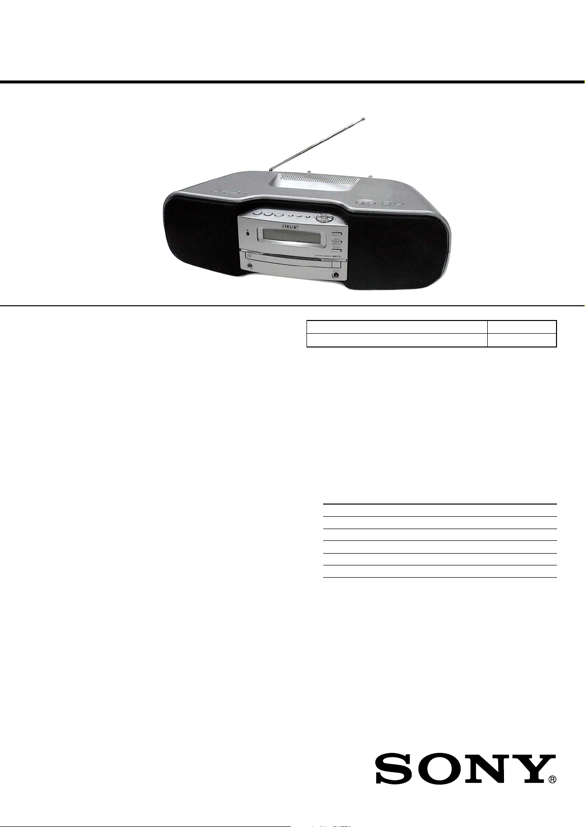
ZS-S50CP
SERVICE MANUAL
Ver. 1.1 2007.08
Model Name Using Similar Optical Pick-up Block NEW
Optical Pick-up Block Type KSM-213CCP
SPECIFICATIONS
CD player section
System
Compact disc digital audio system
Laser diode properties
Emission duration: Continuous
Laser output: Less than 44.6 µW
(This output is the value measured at a distance of about 200 mm from
the objective lens surface on the optical pick-up block with 7 mm
aperture.)
Number of channels
2
Frequency response
20 - 20 000 Hz +1/−1 dB
Wow and flutter
Below measurable limit
Radio section
Frequency range
FM: 87.5 - 108 MHz
AM:
except Mexican model:
531 - 1 611 kHz (9 kHz step)
530 - 1 610 kHz (10 kHz step)
Mexican model:
530 - 1 710 kHz
IF
FM: 10.7 MHz
AM: 450 kHz
Antennas
FM: Telescopic antenna
AM: Built-in ferrite bar antenna
AEP Model
E Model
Power output
4.5 W + 4.5 W (at 6 Ω, 10% harmonic distortion)
Power requirements
For player:
Mexican model: 120 V AC, 60 Hz
Singapore model: 230 - 240 V AC, 50 Hz
Other models: 230 V AC, 50 Hz
9 V DC, 6 R20 (size D) batteries
For remote control:
3 V DC, 2 R6 (size AA) batteries
Power consumption
AC 16 W
Battery life
For player:
FM Radio reception
Sony R20P: approx. 30 h
Sony alkaline LR20: approx. 60 h
CD playback
Sony R20P: approx. 8 h
Sony alkaline LR20: approx. 20 h
It is recommended that you use alkaline batteries.
Dimensions
Approx. 480 × 156 × 250 mm (w/h/d)
(incl. projecting parts)
Mass
Approx. 4.3 kg (incl. batteries)
Supplied accessories
AC power cord (1)
Remote control (1)
General
Speaker
Full range: 10 cm dia., 6 Ω, cone type (2)
Input
AUDIO IN jack (stereo minijack): Minimum input level 245 mV
Outputs
Headphones jack (stereo minijack)
For 16 - 64 Ω impedance headphones
9-887-662-02
2007H05-1
© 2007.08
Sony Corporation
Personal Audio Division
Published by Sony Techno Create Corporation
Design and specifications are subject to change without notice.
PERSONAL AUDIO SYSTEM
Page 2

ZS-S50CP
Notes on chip component replacement
• Never reuse a disconnected chip component.
• Notice that the minus side of a tantalum capacitor may be
damaged by heat.
CAUTION
Use of controls or adjustments or performance of procedures
other than those specified herein may result in hazardous radiation
exposure.
TABLE OF CONTENTS
1. SERVICING NOTES ................................................ 3
2. GENERAL ................................................................... 4
3. DISASSEMBLY
3-1. Disassembly Flow ........................................................... 6
3-2. Cabinet (Lower) Assy...................................................... 7
3-3. Cabinet (Upper) Assy ...................................................... 8
3-4. CD Block ......................................................................... 8
3-5. Main Block Assy ............................................................. 9
3-6. MAIN Board, CD Block Assy......................................... 9
3-7. Speaker (10 cm) (SP101) (L-CH),
Speaker (10 cm) (SP201) (R-CH) ................................... 10
3-8. Belt .................................................................................. 10
3-9. Optical Pick-up Block (KSM-213CCP) .......................... 11
4. TEST MODE ............................................................... 12
5. ELECTRICAL ADJUSTMENTS .......................... 12
6. DIAGRAMS
6-1. Block Diagram – CD SERVO Section – ......................... 15
6-2. Block Diagram – TUNER Section – ............................... 16
6-3. Block Diagram – MAIN Section – .................................. 17
6-4. Block Diagram – POWER SUPPLY Section – ............... 18
6-5. Printed Wiring Boards – CD Section – ........................... 20
6-6. Schematic Diagram – CD Board – .................................. 21
6-7. Printed Wiring Board – TU Board –................................ 22
6-8. Schematic Diagram – TU Board – .................................. 23
6-9. Printed Wiring Boards – JACK Section – ....................... 24
6-10. Printed Wiring Board – MAIN Board – .......................... 25
6-11. Schematic Diagram – MAIN Section (1/2) – .................. 26
6-12. Schematic Diagram – MAIN Section (2/2) – .................. 27
6-13. Printed Wiring Board – LCD Board –............................. 28
6-14. Printed Wiring Boards – KEY Section –......................... 29
6-15. Schematic Diagram – PANEL Section – ......................... 30
6-16. Printed Wiring Boards – POWER SUPPLY Section –.... 32
6-17. Schematic Diagram – POWER SUPPLY Section – ........ 33
SAFETY-RELATED COMPONENT WARNING!!
COMPONENTS IDENTIFIED BY MARK 0 OR DOTTED LINE
WITH MARK 0 ON THE SCHEMATIC DIAGRAMS AND IN
THE PARTS LIST ARE CRITICAL TO SAFE OPERATION.
REPLACE THESE COMPONENTS WITH SONY PAR TS WHOSE
PART NUMBERS APPEAR AS SHOWN IN THIS MANU AL OR
IN SUPPLEMENTS PUBLISHED BY SONY.
7. EXPLODED VIEWS
7-1. Overall Section ................................................................ 42
7-2. Cabinet (Lower) Section.................................................. 43
7-3. Cabinet (Upper) Section .................................................. 44
7-4. Cabinet (Front) Section ................................................... 45
7-5. Front Panel Assy.............................................................. 46
7-6. Main Block Section ......................................................... 47
7-7. Loading Mechanism Section ........................................... 48
7-8. CD Block ......................................................................... 49
8. ELECTRICAL PARTS LIST .................................. 50
2
Page 3
SECTION 1
W
SERVICING NOTES
ZS-S50CP
NOTES ON HANDLING THE OPTICAL PICK-UP
BLOCK OR BASE UNIT
The laser diode in the optical pick-up block may suffer electrostatic
break-down because of the potential difference generated by the
charged electrostatic load, etc. on clothing and the human body.
During repair, pay attention to electrostatic break-down and also
use the procedure in the printed matter which is included in the
repair parts.
The flexible board is easily damaged and should be handled with
care.
NOTES ON LASER DIODE EMISSION CHECK
The laser beam on this model is concentrated so as to be focused on
the disc reflective surface by the objective lens in the optical pickup block. Therefore, when checking the laser diode emission,
observe from more than 30 cm away from the objective lens.
MODEL IDENTIFICATION
– Model Number Label –
MODEL NO.
PERSONAL AUDIO SYSTEM
ZS-S50CP
UNLEADED SOLDER
Boards requiring use of unleaded solder are printed with the leadfree mark (LF) indicating the solder contains no lead.
(Caution: Some printed circuit boards may not come printed with
the lead free mark due to their particular size)
: LEAD FREE MARK
Unleaded solder has the following characteristics.
• Unleaded solder melts at a temperature about 40 °C higher
than ordinary solder.
Ordinary soldering irons can be used but the iron tip has to be
applied to the solder joint for a slightly longer time.
Soldering irons using a temperature regulator should be set to
about 350 °C.
Caution: The printed pattern (copper foil) may peel away if
the heated tip is applied for too long, so be careful!
• Strong viscosity
Unleaded solder is more viscou-s (sticky, less prone to flow)
than ordinary solder so use caution not to let solder bridges
occur such as on IC pins, etc.
• Usable with ordinary solder
It is best to use only unleaded solder but unleaded solder may
also be added to ordinary solder.
Mexican model: AC: 120 V 60 Hz 16 W
Singapore model: AC: 230 - 240 V
Other models: AC: 230 V - 50 Hz 16 W
-
50 Hz 16
3
Page 4

ZS-S50CP
Basic Operations
SECTION 2
Playing a CD/MP3 disc
1
Press CD ȳ on the unit.
“CD” app ears in the display.
2
Press ìȶ on the unit, and place a disc with the
label side up on the CD tray.
To c lose the CD tray, press ì
ȫ
3
Press
on the unit.
à
e unit plays all the tracks/MP3 les once.
When you place MP3 discs, “MP3” appears in the
display aer the unit reads the le information.
Audio CD
Track number Playing time
MP3 disc
ȶ
on the unit.
GENERAL
Tips
Playback starts from the track/MP3 le you last stopped playing
ˎ
(Resume play). During stop, the track/MP3 le number to be played
is displayed.
To cancel the resume play (to start play from the beginning of the
ˎ
rst track/MP3 le), press
you open the CD tray or turn o the unit, the resume play is also
canceled.
Notes
When pressing ȯ (ßˎÑ, ùˎÃ, j, ) on the unit, press
ˎ
the marking at the part near the outer edge.
You cannot locate a specic track if “SHUF” or “PGM” is lit in the
ˎ
display. Press
“SHUF” and “PGM” disappears from the display.
Example of folder structure and playing order
e playing order of the folders and les is as follows:
ȫ
while the CD is stopped. When
Ą
ȫ
, and then press MODE Ȯ repeatedly until
Ą
Folder
MP3 le
This section is extracted from
instruction manual.
Changing the AM tuning interval
Changing the AM tuning interval
If you need to change the AM tuning interval, do the
(except Mexican model)
following:
If you need to change the AM tuning interval, do the
following:
1
Press RADIO BANDˎAUTO PRESET ȴ on the unit
until “AM” is displayed.
1
Press RADIO BANDˎAUTO PRESET ȴ on the unit
until “AM” is displayed.
2
Press ENTER ȯ on the unit for 2 seconds.
2
Press ENTER ȯ on the unit for 2 seconds.
3
Press RADIO BANDˎAUTO PRESET ȴ on the unit for
2 seconds.
3
Press RADIO BANDˎAUTO PRESET ȴ on the unit for
2 seconds.
“9K STEP” or “10K STEP” ashes.
“9K STEP” or “10K STEP” ashes.
4
Press TUNE + or – on the unit to select “9K STEP” for
9 kHz interval or “10K STEP” for 10 kHz interval.
4
Press TUNE + or – on the unit to select “9K STEP” for
9 kHz interval or “10K STEP” for 10 kHz interval.
5
Press ENTER ȯ on the unit.
5
Press ENTER ȯ on the unit.
Aer changing the tuning interval, you need to reset your
preset AM radio stations.
Aer changing the tuning interval, you need to reset your
preset AM radio stations.
*VOLUME + Ȱ and àȫ on the unit have a tactile dot.
Before using the unit
To turn on/o the power
Press POWER ȩ.
To adjust the volume
Press VOLUME +, – Ȱ.
To listen through headphones
Connect the headphones to the (headphones) jack ȸ.
To select the sound characteristic
Press SOUND Ȳ repeatedly to select the audio emphasis
you want.
Choose To get
To reinforce the bass sound
Press MEGA BASS ȱ to display “MEGA BASS” in the
display.
To return to normal sound, press MEGA BASS
disappear from the display.
Powerful, clean sounds, emphasizing low and
high range audio
Light, bright sounds emphasizing high and
middle range audio
Percussive sounds, emphasizing bass audio
The presence of vocals, stressing middle
range audio
The whole dynamic range for music such as
classical music
ȱ
to
MP3 le number After the song title is displayed,
*If the playing time is more than 100 minutes, it appears “--:--” in
the display.
To Pr ess
Pause playba ck
Stop playback
Go to the next track/
MP3 file
Go back to the
previous track/MP3
file
Select a folder on an
MP3 disc
Locate a point while
listening to the sound
Locate a point while
observing the display
Remove the CD
On the remote
To s elect CD function, press FUNCTION Ⱥ repeatedly
to select “CD” in the display.
the playing time* will appear.
ê
ȫ
. To resume play, press it again.
Ą
ȫ
.
ßˎÑ (Ñ
on the remote) ȯ.
ùˎÃ (Ã
on the remote) ȯ.
/PRESET + ( + on the remote)
to go forward and /PRESET – (
– on the remote)ȯ to go backward.
ßˎÑ
(forward) or
or
(forward) or
ù
.
ùˎÃ
ù
ȯ
)
ùˎÃ
ȯ
)
(backward) ȯ while playing and hold it
until you find the point. (On the remote,
ß
use
ßˎÑ
(backward) ȯ in pause and hold it until
you find the point. (On the remote, use
ß
or
ì
ȶ
Notes on MP3 discs
When the disc is inserted, the unit reads all the les on that disc.
ˎ
During this time, “READING” is displayed. If there are many folders
or non-MP3 les on the disc, it may take a long time for play to
begin or for the next MP3 le to start play.
We recommend that you do not save unnecessary folders or les
other than MP3 ones in the disc to be used for MP3 listening.
A folder that does not include an MP3 le is skipped.
ˎ
Maximum number of les: 255
ˎ
Maximum number of folders: 150 (including the root folder)
ȯ
Maximum number of folders and les in total: 300
Maximum directory levels: 8
Folder names and le names can be displayed with up to 32
ˎ
characters including quotation marks.
e characters A - Z, 0 - 9, and _ can be displayed on this unit.
ˎ
Other characters are displayed as “_”.
is unit conforms to Version 1.0, 1.1, 2.2, 2.3 and 2.4 of the ID3 tag
ˎ
format. When the le has the ID3 tag information, “song title”, “artist
name” and “album name” can be displayed. If the le does not have
the ID3 tag information, “NO TITLE” appears instead of song title,
“NO ARTIST” appears instead of artist name and “NO ALBUM”
appears instead of album name. e ID3 tag information can be
displayed with up to 30 characters.
e characters may not be displayed correctly according to the
ˎ
character code.
When naming, be sure to add the le extension “mp3” to the le
ˎ
name.
If you put the extension “mp3” to a le other than an MP3 le, the
ˎ
unit cannot recognize the le properly and will generate random
noise that could damage your speakers.
e le name does not correspond to the ID3 tag.
ˎ
Listening to the radio
To listen to FM or AM
1
Press RADIO BANDˎAUTO PRESET ȴ on the unit
BANDȴ on the remote) repeatedly to
(RADIO
ˎ
select FM or AM.
2
Hold down TUNE + or – ȯ until the frequency digits
begin to change in the display.
e unit automatically scans the radio frequencies and
stops when it nds a clear station.
If you cannot tune in a station, press TUNE + or –
repeatedly to change the frequency step by step.
When an FM stereo broadcast is received, “ST”
appears.
Tip
If the FM broadcast is noisy, press MODE Ȯ until “MONO” appears
in the display and the radio will play in monaural.
ȯ
4
Page 5
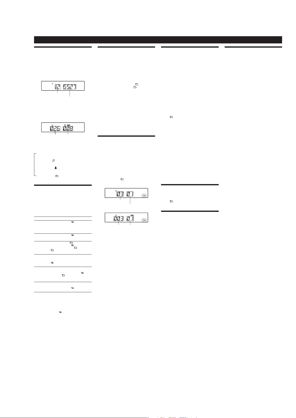
Using the display
You ca n check information about the CD using the
display.
Checking the information of an audio CD
To check the total track number and playing
time of the CD
Press Ąȫ to stop the CD playback.
Total track number
Total playing time
Checking the information of an MP3 disc
To check the total folder number and total le
number on the CD
Press Ąȫ while the CD is stopped, and you can check
them in the display.
Total le number Total folder number
To check le information
Press DISPLAY Ȭ on the unit while playing an MP3
disc. e display changes as follows:
e current le number and playing time
Ô
e song title (
)
e artist name (
)
e album name (
)
Playing tracks/MP3 les repeatedly
(Repeat Play)
You can play tracks/MP3 les repeatedly in normal,
Shue or Program play modes.
1 Press CD
ȳ
.
“CD” app ears in the display.
2 Proceed as follows.
To repeat Do this
A single
track/MP3
file
1Press REPEAT
ȭ
until “ 1” appears.
2Press
Ãˎù
or
ßˎÑ (Ã
or Ñ on the
remote)
ȯ
to select the track/MP3 le that you
want to repeat.
3Press
à
ȫ
.
All tracks/
MP3 files on
the CD
1Press REPEAT
ȭ
until “ ” appears.
2Press
à
ȫ
.
A selected
folder (MP3
disc only)
1Press MODE
Ȯ
until “ ” appears, and then
press REPEAT
ȭ
until “ ” appears.
2Select the folder by pressing
/PRESET + or –
(
+ or – on the remote) ȯ.
3Press
à
ȫ
.
Tracks/MP3
files in
random
order
1Select Shue Play (see “Playing tracks/MP3 les
in random order”).
2Press REPEAT
ȭ
until “SHUF” and
“
” appear.
3Press
à
ȫ
.
Files in a
selected
folder in
random
order (MP3
disc only)
1Start Folder Shue Play (see “Playing tracks/
MP3 les in random order”).
2Press REPEAT
ȭ
on the unit until “ ”,
“SHUF” and “
” appear.
3Press
à
ȫ
.
Programed
tracks/MP3
files
1Program tracks/MP3 les (see “Creating your
own program”).
2Press REPEAT
ȭ
until “ ” and “PGM” appear.
3Press
à
ȫ
.
On the remote
To s elect the CD function, press FUNCTION
Ⱥ
repeatedly until “CD” appears in the display.
To c ancel Repeat Play
Press REPEAT ȭ until “ ” disappears from the display.
Other Operations
Playing tracks/MP3 les in random
order
(Shue Play)
You can play tracks/MP3 les in random order. When
playing an MP3 disc, you can also play MP3 les in a
selected folder in random order (Folder Shue Play).
1 Press CD
ȳ
.
“CD” app ears in the display.
2 Press MODE
Ȯ
until “SHUF” appears in the display.
When you select Folder Shue Play (MP3 disc only),
press MODE
Ȯ
on the unit until “ ” and “SHUF”
appear in the display. en press
/PRESET + or
–
ȯ
on the unit to select a folder you want.
3 Press à
ȫ
on the unit to start Shue Play.
On the remote
To s elect the CD function, press FUNCTION Ⱥ
repeatedly until “CD” appears in the display.
To cancel Shue Play
Stop playing rst. en press MODE Ȯ repeatedly until
“SHUF” disappears from the display.
Tips
ˎ
During Shue Play, you cannot select the previous track/MP3 le by
pressing
ùˎÃ (Ã
on the remote) ȯ.
ˎ
e resume function does not work during Shue Play.
Creating your own program
(Program Play)
You can arrange the playing order of up to 20 tracks on
a CD.
1 Press CD
ȳ
.
“CD” app ears in the display.
2 Press MODE
Ȯ
repeatedly until “PGM” ashes in the
display.
3 Press
ùˎÃ
or
ßˎÑ (Ã
or Ñon the
remote)
ȯ
then press ENTER ȯ for the track/MP3
les you want to program in the order you want.
For MP3 les, press
/PRESET + or – ȯ rst and
then press ENTER
ȯ
.
Audio CD (Program Play)
Programed track number
Playing order
MP3 disc (Program Play)
Programed track number Playing order
4 Press à
ȫ
to start Program Play.
On the remote
To s elect the CD function, press CD ȳ.
To c ancel Program Play
Stop playing rst. en press MODEȮ repeatedly until
“PGM” disappears from the display.
To delete the last track of the program
Press CLEAR Ȼ on the remote while the player is
stopped.
To check the order of tracks before play
Press ENTERȯ.
Every time you press the button, the track number
appears in the programed order.
To change the current program
Press Ąȫ once if the CD is stopped and twice if the
CD is playing. e current program will be erased.
en create a new program following the programing
procedure.
Tips
ˎ
If you try to program 21 tracks/MP3 les or more, “FULL” will
appear in the display.
ˎ
You can play the same program again, since the program is saved
until you open the CD tray or turn o the power of the unit.
ˎ
e resume function does not work during Program Play.
Presetting radio stations
You can store radio stations into the unit’s memory. You
can preset up to 30 radio stations, 20 for FM and 10 for
AM in any order.
1 Press RADIO BAND
ˎ
AUTO PRESET ȴ on the unit to
select the band.
2 Hold down RADIO BAND
ˎ
AUTO PRESET ȴ on the
unit for 2 seconds until “AUTO” ashes in the display.
3 Press ENTER
ȯ
while “AUTO” ashes in the display.
e stations are stored in memory from the lower
frequencies to the higher ones.
If a station cannot be preset automatically
You need to preset a station with a weak signal manually.
1 Press RADIO BAND
ˎ
AUTO PRESET ȴ on the unit to
select the band.
2 Tune in a station you want.
3 Hold down ENTER
ȯ
on the unit for 2 seconds until
the preset number ashes in the display.
4 Press /PRESE T + or –
ȯ
on the unit until the
preset number you want for the station ashes in
the display.
5 Press ENTER
ȯ
on the unit.
e new station replaces the old one.
On the remote
1 Press RADIO
ˎ
BANDȴ repeatedly until the band
you want appears in the display.
2 Tune in a station you want.
3 Hold down ENTER
ȯ
for 2 seconds until the preset
number ashes in the display.
4 Press PRESET + or –
ȯ
until the preset number you
want for the station ashes in the display.
5 Press ENTER
ȯ
.
e new station replaces the old one.
Tip
e preset radio stations remain in memory even if you unplug the
AC power cord or remove the batteries.
Playing preset radio stations
1 Press RADIO BAND
ˎ
AUTO PRESET ȴ on the unit
(RADIO
ˎ
BANDȴ on the remote) to select the band.
2 Press /PRESE T + or –
ȯ
on the unit (PRESET + or
–
ȯ
on the remote) to tune in the stored station.
Falling asleep to music
1 Play the music source you want.
2 Press SLEEP
ȹ
on the unit to display “SLEEP”.
3 Press SLEEP
ȹ
on the unit to select the minutes
until the unit goes o automatically.
Each time you press the button, the indication changes
as follows:
“AUTO*” “60MIN” “30MIN” “20MIN”
“10MIN” “OFF”.
*When you select “AUTO”, the CD stops playing in 90 minutes at
most and the unit goes o automatically. When you are listening
to the radio, the radio goes o in 90 minutes.
If 4 seconds have passed aer you pressed SLEEP ȹ,
the minutes in the display are entered.
When the preset time has passed, the unit goes o
automatically.
To cancel the sleep function
Press POWER ȩ to turn o the power.
Tip
e display’s backlight goes o while sleeping time is active.
Connecting optional component
You can enjoy the sound from a PC, TV, VCR, portable
digital music player, etc. through the speakers of this unit.
Be sure to turn o the power of each component before
making any connections.
For details, refer to the instruction manual of the
component to be connected.
1 Connect the AUDIO IN jack ȷ on the unit to the
line output jack of the portable digital music player
or other components using an audio connecting
cable* (not supplied).
*For a PC: use a cable which lls the connector of your PC.
For a TV or VCR: use a cable with a stereo-mini plug on one
end and two phono plugs on the other end.
For a portable digital music player: use a cable with a stereomini plug on both ends.
2 Turn the unit and the connected component on.
3 Press AUDIO IN ȵ and start playing sound on the
connected component.
e sound from the connected component is output
from the speakers.
ZS-S50CP
5
Page 6
ZS-S50CP
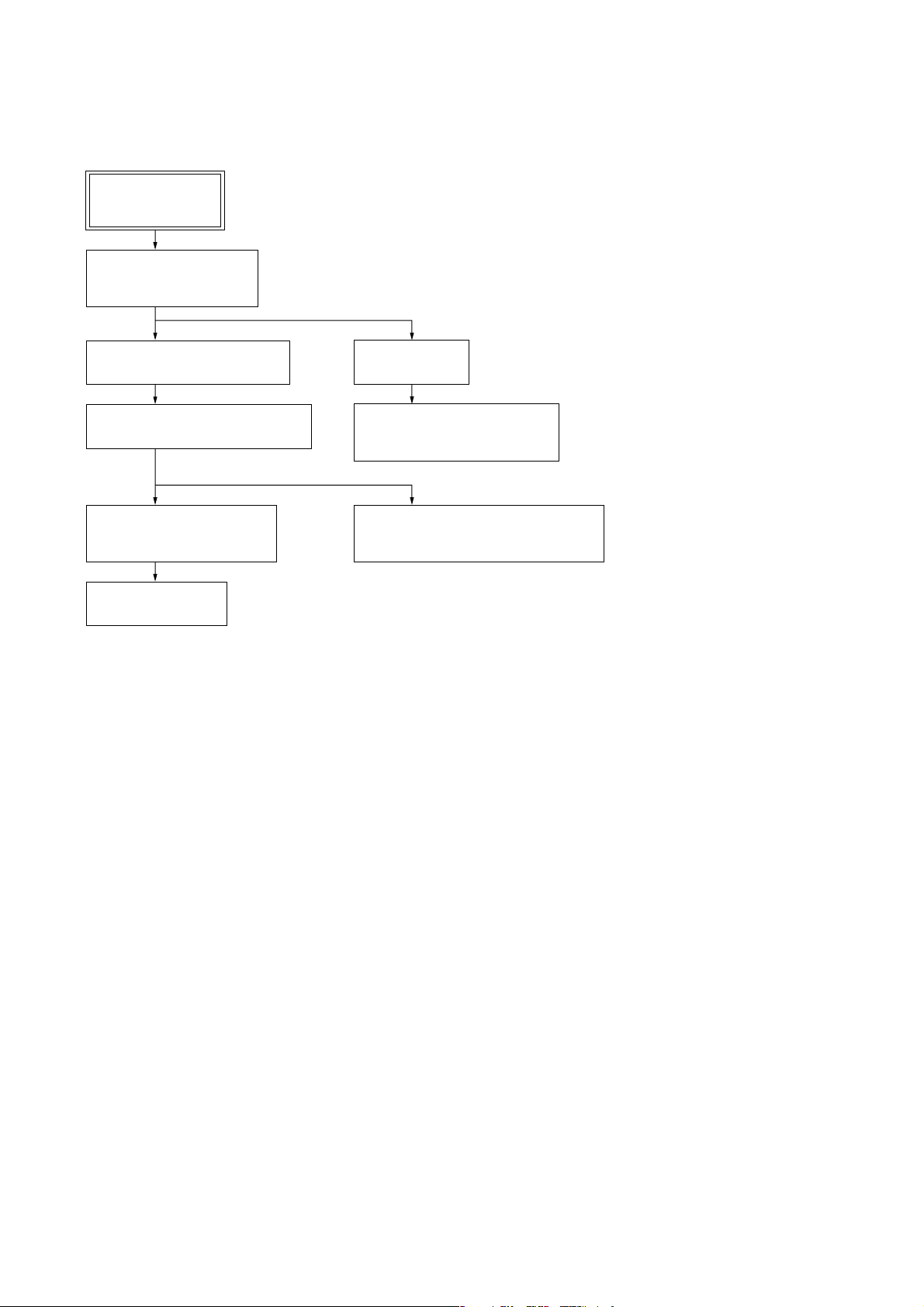
• This set can be disassembled in the order shown below.
3-1. DISASSEMBLY FLOW
SET
3-2. CABINET (LOWER)
ASSY
(Page 7)
SECTION 3
DISASSEMBLY
3-3. CABINET (UPPER) ASSY
(Page 8)
3-5. MAIN BLOCK ASSY
(Page 9)
3-6. MAIN BOARD,
CD BLOCK ASSY
(Page 9)
3-8. BELT
(Page 10)
3-4. CD BLOCK
(Page 8)
3-9. OPTICAL PICK-UP BLOCK
(KSM-213CCP)
(Page 11)
3-7. SPEAKER (10 cm) (SP101) (L-CH),
SPEAKER (10 cm) (SP201) (R-CH)
(Page 10)
6
Page 7
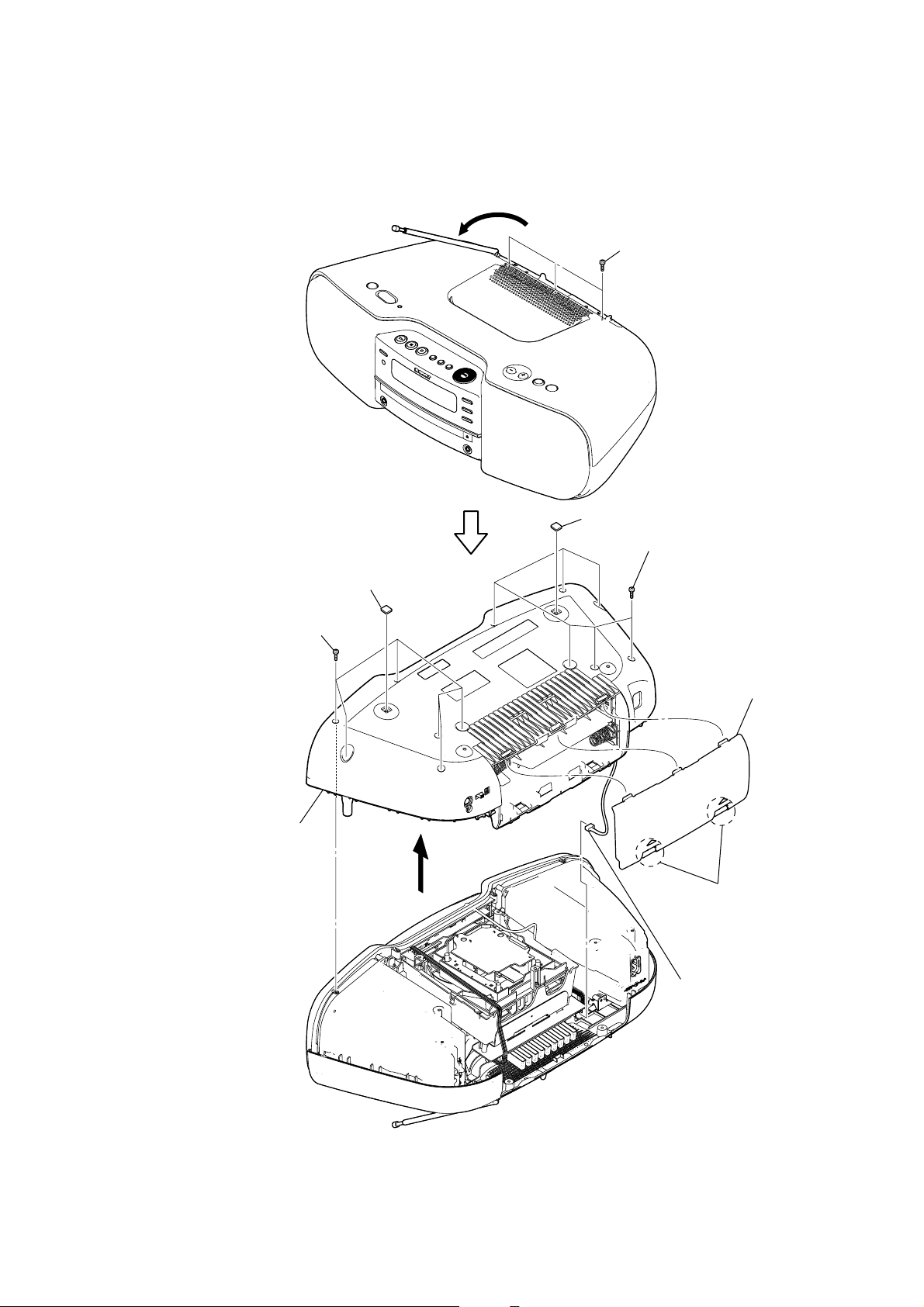
Note: Follow the disassembly procedure in the numerical order given.
3-2. CABINET (LOWER) ASSY
1
2
three screws
(B2.6)
ZS-S50CP
5
9
cabinet (lower) assy
six screws
(B2.6)
8
foot (felt)
Turn the set.
6
8
foot (felt)
5
six screws
(B2.6)
4
battery case lid
3
Release two hooks.
7
connector
(CN901)
7
Page 8
ZS-S50CP
)
3-3. CABINET (UPPER) ASSY
3
two screws
(B2.6)
4
screw
(B2.6)
5
screw
(P2.6
×
10)
flexible flat cable (4 core)
7
(CNP810)
6
4
screw
(B2.6)
5
screw
(P2.6
×
10)
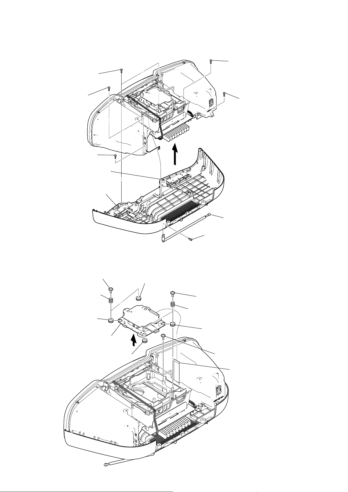
3-4. CD BLOCK
3
two springs (insulator)
8
cabinet (upper) assy
2
two floating screws
5
insulator
6
CD block
5
4
insulator
5
insulator
2
two floating screws
3
two springs
(insulator)
5
1
screw
(M3)
insulator
2
telescopic antenna
(ANT1)
2
floating screw
1
flexible flat cable
(21 core) (CNP201
8
Page 9
3-5. MAIN BLOCK ASSY
y
8
flexible flat cable (11 core)
(CNP806)
7
flexible flat cable (11 core)
(CNP802)
2
connector
(CN306)
1
connector
(CN309)
5
screw
(B2.6)
3
4
connector
(CN310)
5
screw
(B2.6)
connector
(CN902)
6
0
main block ass
ZS-S50CP
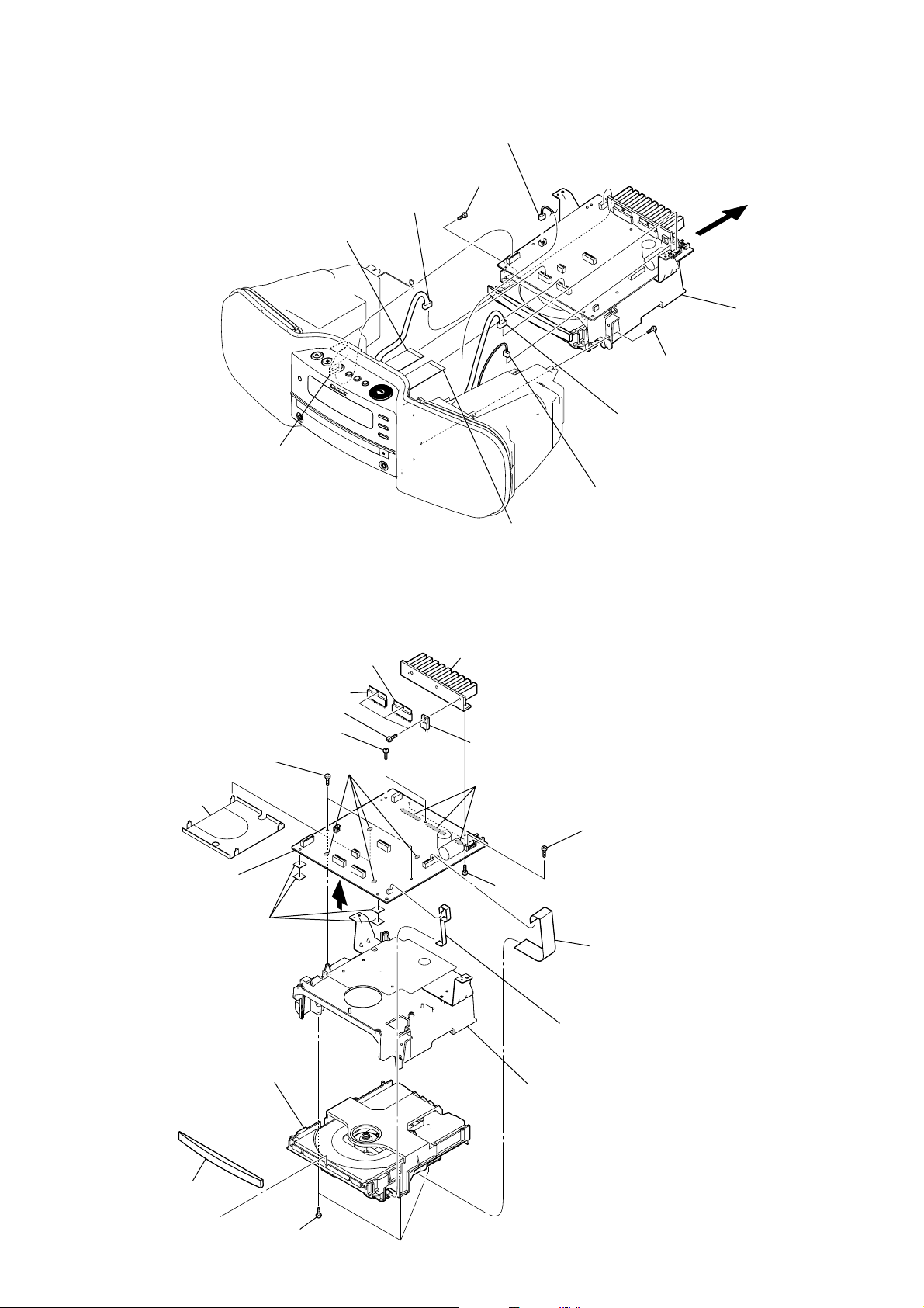
3-6. MAIN BOARD, CD BLOCK ASSY
qa
IC BA5417 (IC304)
qa
IC BA5417 (IC305)
0
three screws (B2.6)
3
two screws (B2.6)
6
3
7
shield plate
(main PWB)
qd
two screws (B2.6)
MAIN board
5
four sheets (1)
four
solders
4
9
flexible flat cable (7 core)
(CNP807)
qs
heat sink assy
qa
transistor 2SD2394-F
9
three solders
8
two screws (B2.6)
3
screw (B2.6)
1
flexible flat cable (14 core)
(with sield (FFC): AEP, Italian, East European,
Russian models)
(MAIN board: CNP803, CD board: CNP201)
qf
panel (CD)
qj
CD block assy
qg
three screws (B3)
2
qh
chassis block
flexible flat cable (5 core)
(MAIN board: CNP805, MOTOR board: CN001)
9
Page 10
ZS-S50CP
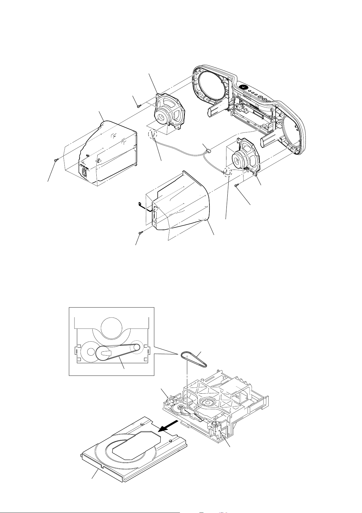
3-7. SPEAKER (10 cm) (SP101) (L-CH), SPEAKER (10 cm) (SP201) (R-CH)
6
speaker (10 cm)
(SP201) (R-CH)
5
four screws
(B3)
2
speaker box (R) section
3
connector
(CN311)
4
Remove two solders.
1
six screws
(B2.6)
6
speaker (10 cm)
(SP101) (L-CH)
3-8. BELT
position of belt
1
six screws
(B2.6)
belt
4
Remove two solders.
2
speaker box (L) section
4
belt
5
four screws
(B3)
10
3
tray (AU)
2
claw
1
2
claw
Page 11
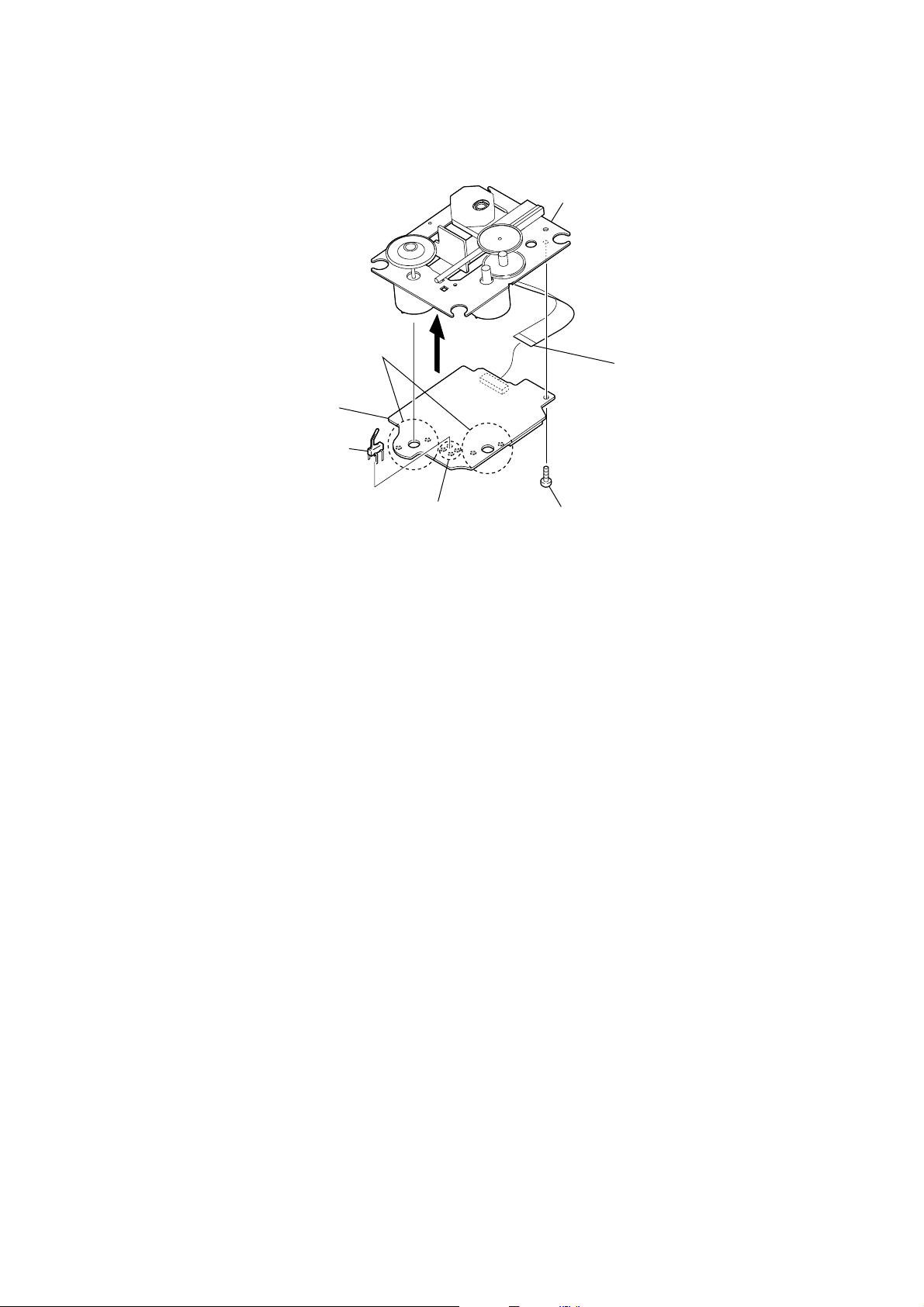
3-9. OPTICAL PICK-UP BLOCK (KSM-213CCP)
1
Remove four solders.
7
CD board
6
detection switch (limit)
(S201)
4
optical pick-up block
(KSM-213CCP)
2
ZS-S50CP
flexible flat cable (16 core)
(CN301)
5
Remove four solders.
3
screw
(BVTT2
×
6)
11
Page 12
ZS-S50CP
+
–
CD board
TP121 (RFI)
TP124 (VC)
oscilloscope
(DC range)
V
SECTION 4
TEST MODE
SECTION 5
ELECTRICAL ADJUSTMENTS
COLD RESET
Procedure:
1. In the power on status, press three buttons of [ENTER], x ,
[POWER] simultaneously.
2. The set is reset and display “RESET”, then becomes standby
status.
PANEL TEST MODE
Procedure:
1. In the standby mode or power on status, press three buttons of
[ENTER], [SLEEP], [DISPLAY] simultaneously.
2. When enter this mode, it turns on all segments of the liquid
crystal display.
3. In this mode, it displays as follows.
[BAND] button : Date/Version display
[AUDIO IN] button: Destination display
4. To exit from this mode, press three buttons of [ENTER],
[SLEEP], [DISPLAY] simultaneously.
CHANGE OF THE AM TUNING INTERVAL
(except Mexican model)
Procedure:
1. Press the [POWER] button to turn the power on.
2. Press the [BAND] button to select “AM”.
3. Press the [ENTER] button for 2 seconds, and then press the
[BAND] button for 2 seconds, “9K STEP” or “10K STEP” is
displayed on the liquid crystal display.
4. The AM tuning interval is selected by pressing the [TUNE +]/
[TUNE ---] button, and it is fix ed by pressing the [ENTER] button.
CD SECTION
Note:
1. CD Block is basically constructed to operate without adjustment.
2. Use YEDS-18 disc (3-702-101-01) unless otherwise indicated.
3. Use an oscilloscope with more than 10 MΩ impedance.
4. Clean the object lens by an applicator with neutral detergent when the
signal level is low than specified value with the following checks.
5. Check the focus bias check when optical pick-up block is replaced.
FOCUS BIAS CHECK
Procedure :
1. Connect oscilloscope to TP121 (RFI) and TP124 (VC) on the
CD board.
2. Press the [POWER] button to turn the power ON and press the
[CD] button to set the “CD” function.
3. Set disc (YEDS-18) on the tray and press the N button to
playback.
4. Confirm that oscilloscope waveform is as sho wn in the figure
below. (eye pattern)
A good eye pattern means that the diamond shape (◊) in the
center of the waveform can be clearly distinguished.
VOLT/DIV: 200 m
TIME/DIV: 500 ns
Checking Location:
– CD Board (Conductor Side) –
TP124
(VC)
TP121
(RFI)
IC101
level:
1.2
±
0.3 Vp-p
12
Page 13
ZS-S50CP
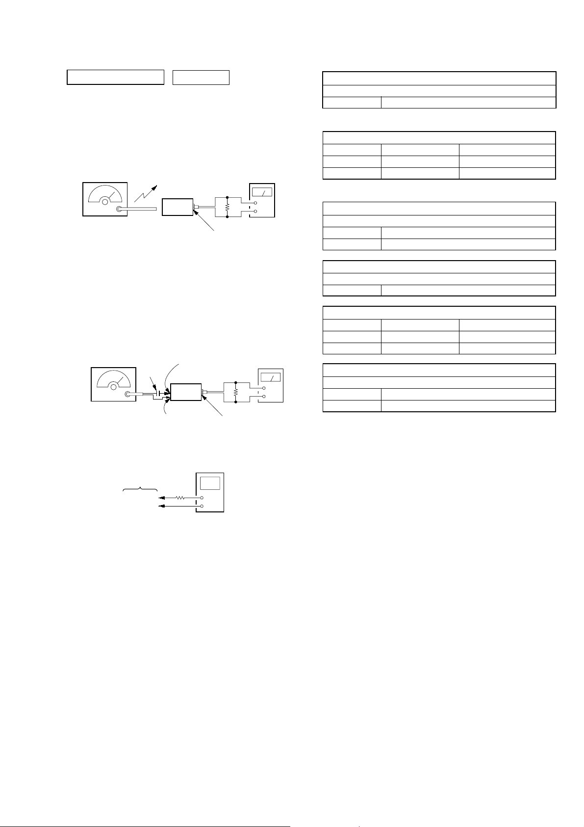
TUNER SECTION 0 dB=1 µV
[AM]
Setting:
Function: RADIO
Band: AM
AM RF signal
generator
30% amplitude
modulation by
400 Hz signal
Output level:
as low as possible
[FM]
Setting:
Function: RADIO
Band: FM
FM RF signal
generator
75 kHz frequency
deviation by 1 kHz
signal
Output level:
as low as possible
Put the lead-wire
antenna close to
the set.
set
TU board
TP (ANT)
0.01 µF
set
TU board
TP (GND)
level meter
32
Ω
+
–
JACK (HP) Board
i
jack (J301)
level meter
32
Ω
+
–
JACK (HP) Board
i
jack (J301)
AM IF ADJUSTMENT
Adjust for a maximum reading on level meter
T1 450 kHz
(): except Mexican model
AM FREQUENCY COVERAGE ADJUSTMENT
Adjustment Part Frequency Display Reading on Digital Voltmeter
L4 530 kHz (531 kHz) 1.0 ± 0.3 V
Confirmation 1,710 kHz (1,611 kHz) 5.2 ± 0.8 V (4.8 ± 0.6 V)
(): except Mexican model
AM TRACKING ADJUSTMENT
Adjust for a maximum reading on level meter
L3 620 kHz (621 kHz)
CT3 1,400 kHz (1,404 kHz)
FM IF ADJUSTMENT
Adjust for a minimum reading on level meter
T2 10.7 MHz
FM FREQUENCY COVERAGE ADJUSTMENT
Adjustment Part Frequency Display Reading on Digital Voltmeter
L2 108 MHz 3.0 ± 0.3 V
Confirmation 87.5 MHz 1.3 ± 0.4 V
FM TRACKING ADJUSTMENT
Adjust for a maximum reading on level meter
L1 87.5 MHz
CT1 108 MHz
Adjustment and Connecting Locations: TU board (see page 14)
digital voltmeter
TU board
100 k
TP (VT)
TP (GND)
Ω
• Repeat the procedures in each adjustment several times, and
the tracking adjustments should be finally done by the trimmer
capacitors.
• Remove FM antenna in FM adjustment.
13
Page 14
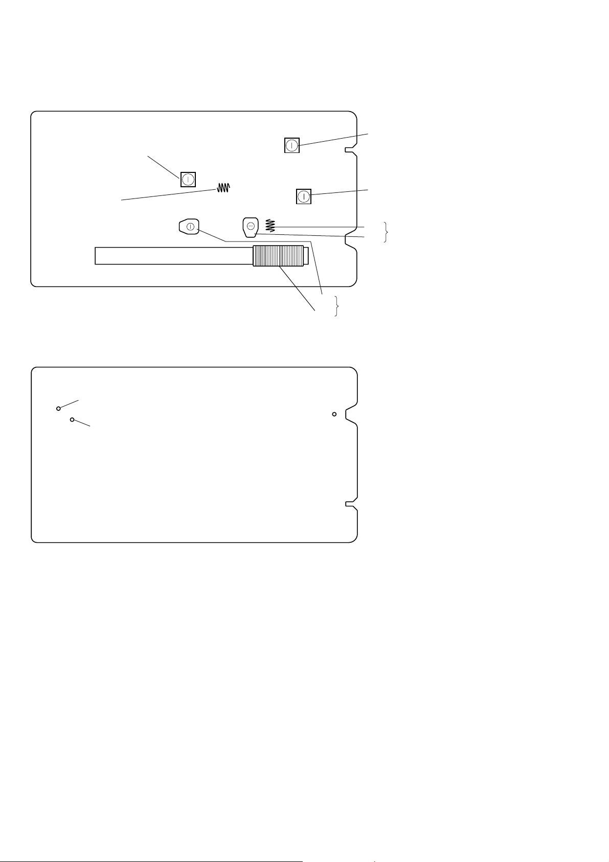
ZS-S50CP
Adjustment and Connecting Location:
– TU Board (Component Side) –
AM Frequency Coverage Adjustment
L4
L2
FM Frequency Coverage Adjustment
– TU Board (Conductor Side) –
TP
(VT)
TP
(GND)
T2 FM IF Adjustment
T1 AM IF Adjustment
L1
CT1
CT3
AM T rac king Adjustment
L3
TP
(ANT)
FM T rac king Adjustment
14
Page 15

SECTION 6
DIAGRAMS
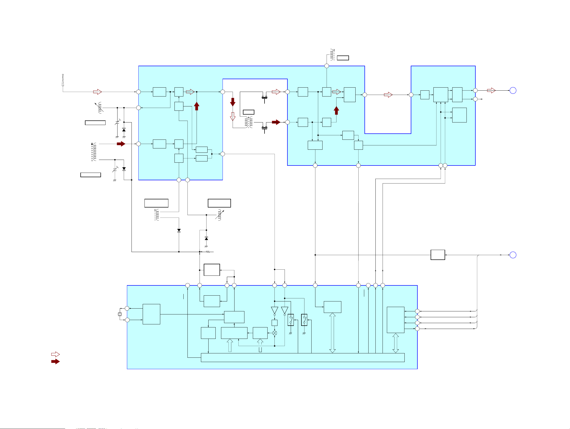
6-1. BLOCK DIAGRAM – CD SERVO Section –
CD
DETECTOR
A
B
C
D
E
F
LASER DIODE
I-V AMP
VCC
+3.3V
A
B
C
D
E
F
FNi1 (A)
95
97 FPi1 (B)
94 FNi2 (C)
96 FPi2 (D)
100 TNi (E)
98 TPi (F)
RFo
89
3RFRP RFZI
88
2
76TEi TEZi
AGCi
83RFEQo 81 RFi
82 RFRPi
ZS-S50CP
30LO
27RO
R-CH
CD-L
A
(Page 17)
PD
LD
OPTICAL PICK-UP
BLOCK
(KSM-213CCP)
M401
(SPINDLE)
M402
(SLED)
2-AXIS
DEVICE
(TRACKING)(FOCUS)
LD
PD
VC
SP+
M
SP–
SL+
M
SL–
T+
T–
F+
F–
AUTOMATIC
POWER CONTROL
Q301
91 LDo 92MDi
FOCUS/TRACKING COIL DRIVE,
SLED/SPINDLE MOTOR DRIVE
2 VO1+
1 VO1–
12 VO2–
11 VO2+
18 VO3+
17 VO3–
26 VO4+
VO4–
27
IC401
MUTE
7
BIAS
IN1
IN2’
IN3’
IN4’
23
3
9
20
24
84 VRo
13 DMo
12 FMo
10 TRo
9 FOo
CD-MP3 PROCESSOR
IC101
38BUS0
39BUS1 59 BUS1
40BUS2 (SO) 60 BUS2
41BUS3 (SI) 61 BUS3
42BUCK (CLK)
43XCCE
48PIO0
58 BUS0
66 BUCK
67 CCEN
68 REQ
SYSTEM CONTROLLER
IC803 (1/3)
ZS-S50CP
R-ch is omitted due to same as L-ch.
SIGNAL PATH
: CD PLAY
CD
+3.3V
S201
(LIMIT)
20 IO0 (/HSO)
XI
23
X102
16.9344MHz
O-TRY-CLS 89
O-TRY-OPN
54SBSY
37XRST
XO
24
57 SBSY
70 MP3/CD-RST
69 MMUTE
I-TRY-OPN
I-TRY-CLS
90
92
91
LOADING
MOTOR DRIVE
IC601
OPEN/CLOSE DETECT
S001
DISC TRAY
OPEN
CLOSE
M
M001
(LOADING)
1515
Page 16
ZS-S50CP
6-2. BLOCK DIAGRAM – TUNER Section –
FM/AM RF AMP, MIX, OSC,
FM/AM IF AMP, DET, MPX
ANT1
FM TELESCOPIC
ANTENNA
IC1
10
QUAD
T2
FM IFT
FM IF
L1
FM RF
CT1, L1
FM TRACKING
L3
AM FERRITE-ROD
ANTENNA
CT3, L3
AM TRACKING
CT1
CT3
D3
(1/2)
FM
RF-IN
2
24
D1
22
RF AMP
FM
RF-OUT
AM
RF-IN
RF AMP
L4
AM OSC
AM FREQUENCY
COVERAGE
FM
AM
D3
(2/2)
FM
MIX
FM
OSC
AM
MIX
AM
OSC
AM OSC
20 21
FM OSC
BUFFER
BUFFER
MIX-OUT
4 7
AM IFT
AM IF
OSC
-OUT
19
L2
FM OSC
FM FREQUENCY
COVERAGE
D2
CF2
T1
CF4
FM
IF-IN
FM IF
AMP
AM
IF-IN
AM IF
6
AMP
FM
DET
AM
DET
IF
BUFFER
IF-OUT
17 18
AF
BUFFER
LEVEL
DET
DET
-OUT
ST
IND
ST-IND
MPX
-IN
AF
16
15
AMP
MPX
LPF1/BAND
LPF2/MO-ST
13
14
MUTE
STEREO/
MONO,
FM/AM
L-OUT
R-OUT
12
11
R-CH
RA-L
B
(Page 17)
• R-ch is omitted due to same as L-ch.
• SIGNAL PATH
: FM
: AM
X1
75kHz
VT B+
LOW-PASS
FILTER
6
PD
LP-OUT
MW/LW
XOUT
20
19
XIN
REFERENCE
DIVIDER
FM/AM PLL
IC2
LOW-PASS
FILTER
UNLOCK
DETECT
LP-IN
PHASE
DETECTOR/
CHARGE PUMP
12 BIT
PROGRAMMABLE
DIVIDER
SWALLOW
COUNTER
111218
FM IN
AM IN
1/2
SHIFT REGISTER & LATCH
10 9
IF IN
UNIVERSAL
COUNTER
ST-IND
BAND
7
BAND
13817 16
MO/ST
CCB
INTERFACE
DI
2
CL
3
CE
1
DO
4
MUTING
Q801
R MUTING
R DATA
R CLOCK
R CE
R COUNT
R DATA, R CLOCK, R CE,
R COUNT, R MUTING
C
(Page 17)
ZS-S50CP
1616
Page 17
6-3. BLOCK DIAGRAM – MAIN Section –
(Page 15)
(Page 16)
CD-L
A
RA-L
B
J302
AUDIO IN
R-CH
INPUT SELECTOR,
ELECTRICAL VOLUME
IC302
L2-IN
5
L1-IN
4
L4-IN
7
L-IGOUT
8
L-VOLIN
9
22
DATA21CLK
L-OUT
ZS-S50CP
R-CH
MEGA BASS
CONTROL
Q101
27
MUTING
Q102
R-CH
R-CH
POWER AMP
IC304
POWER AMP
IC305
+
SP201
(R-CH)
SP101
(L-CH)
J301
i
(Page 16)
R DATA, R CLOCK, R CE,
R COUNT, R MUTING
C
5.53MHz
X802
R DATA
R CLOCK
R CE
R COUNT
R MUTING
SHIFT CLOCK
Q802, 803
RESET SIGNAL
GENERATOR
IC802
EEPROM
IC805
TU-DATA
97
TU-CLK
98
TU-CE
96
TU-COUNT
99
TU-BMUTE
100
X0
82
X1
83
CLKSFT-AM
85
CLKSFT-FM
86
77
21
22
XRESETSYS +3.3V
ROM-SDA
ROM-SCL
33
34
VOL-DATA
VOL-CLK
SYSTEM CONTROLLER
IC803 (2/3)
48
A-MUTE
53
BASS-ON
LCD-SO
LCD-SCK
LCD-CSB
LCD-INHB
LCD-RSTB
I-KEY0 – I-KEY2
I-WAKEUP
O-BK-LIGHT
19
20
14
12
13
47
1
44 – 46
WAKE UP
SWITCH
Q806
SW +9V
LED DRIVE
Q402
LCD DRIVER
IC402
SI
47
SCK
48
CSB
INHB
RSTB
SEG1 – SEG32
COM1 – COM4
S401 – 405,
S407 – 422
D404
OPR/BATT
D402, 403
(LCD BACK LIGHT)
46
44
45
SEG1 – SEG32
5 – 12,
14 – 25, 27 – 38
COM1 – COM4
1 – 4
32 – 136 – 33
LCD401
LIQUID
CRYSTAL
DISPLAY
ZS-S50CP
R-ch is omitted due to same as L-ch.
SIGNAL PATH
: FM
: CD PLAY
I-RMC
64
REMOTE CONTROL
RECEIVER
IC401
: AUDIO IN
1717
Page 18
ZS-S50CP
6-4. BLOCK DIAGRAM – POWER SUPPLY Section –
AMP B+
LCD-VDDON
BATCHK-H
REG6V-CHK
REG3V-CHK
CD-ON
SYSTEM CONTROLLER
IC803 (3/3)
SYS +3.3V
LCD +3.3V
3
RMC +3.3V
43
38
39
+1.5V
CD +1.5V
CD +3.3V
54
CD POWER
ON/OFF SWITCH
Q909, 910
REG +6.2V
VOL B+
VT B+
SW +9V
REGULATOR
IC201
B+ SWITCH
Q915
D913
+3.3V
REGULATOR
Q913
D914
B+ SWITCH
Q807, 812
B+ SWITCH
Q808, 809
D805
B+ SWITCH
Q814, 815
+6.2V
REGULATOR
Q907
+3.3V
REGULATOR
IC801
B+ SWITCH
Q904, 906
D917
RECT
D901 – 904
F902
T901
POWER
TRANSFORMER
J901
AC IN
O-PCONT
I-AC/DC
BATCHK-M
56
55
41
AC POWER
SUPPLY DETECT
Q804
BATTERY
VOLTAGE DETECT
Q810, 811. 816
MAIN POWER
ON/OFF SWITCH
Q905
DRY BATTERY
SIZE "D"
(IEC DESIGNATION R20)
6PCS. 9V
ZS-S50CP
1818
Page 19

ZS-S50CP
Ver. 1.1
• Note for Printed Wiring Boards and Schematic Diagrams
Note on Printed Wiring Board:
• X : parts extracted from the component side.
• Y : parts extracted from the conductor side.
• W : indicates side identified with part number.
• f : internal component.
• : Pattern from the side which enables seeing.
(The other layers' patterns are not indicated.)
Caution:
Pattern face side: Parts on the pattern face side seen from
(Conductor Side) the pattern face are indicated.
Parts face side: Parts on the parts face side seen from
(Component Side) the parts face are indicated.
• Indication of transistor
C
Q
B
E
These are omitted.
Note on Schematic Diagram:
• All capacitors are in µF unless otherwise noted. (p: pF)
50 WV or less are not indicated except for electrolytics
and tantalums.
• All resistors are in Ω and 1/
specified.
• f : internal component.
• C : panel designation.
Note: The components identified by mark 0 or dotted line
with mark 0 are critical for safety.
Replace only with part number specified.
• A : B+ Line.
• H : adjustment for repair.
• Power voltage is dc 4.5 V and fed with regurated dc pow er
supply from pin 1 and 4 of KH905 on the TERMINAL
(A) board, and power voltage is dc 9 V and fed with
regurated dc power supply from pin 3 and 4 of KH905
on the TERMINAL (A) board.
• Voltages and waveforms are dc with respect to ground
under no-signal (detuned) conditions.
– CD Board –
no mark :CD PLAY
– TU Board –
no mark : FM
(): AM
– Other Boards –
no mark : FM
(): CD PLAY
• Voltages are taken with a V OM (Input impedance 10 MΩ).
Voltage variations may be noted due to normal production tolerances.
• Waveform are taken with a oscilloscope.
Voltage variations may be noted due to normal production tolerances.
• Circled numbers refer to waveform.
• Signal path.
F : FM
f : AM
J : CD PLAY
i : AUDIO IN
• Abbreviation
EE : East European model
IT : Italian model
MX : Mexican model
RU : Russian model
SP : Singapore model
TH : Thai model
4
W or less unless otherwise
• Circuit Boards Location
PANEL (TOP) board
KEY (TOP-L) board
LCD board
JACK (HP) board
TU board
JACK (AU IN) board
MOTOR board
MAIN board
KEY (TOP-R) board
TERMNAL (B) board
CD board
TERMNAL (A) board
POWER board
ZS-S50CP
1919
Page 20

ZS-S50CP
6-5. PRINTED WIRING BOARDS – CD Section –
1
2 3 4 567 8 9
A
CD BOARD
B
(COMPONENT SIDE)
C401
C405
C
R212
R211
D
C207
IC201
5
C206
314
R201
E
C202
C204
C201
C205
X102
C115
R112
R111
C133
R155
C130
C128
C309
Q301
: Uses unleaded solder.• See Page 19 for Circuit Boards Location.
CD BOARD
TP121
(RFI)
C106
C306
R303
R302
E
C307
R301
R304
1-872-135-
11
(11)
(CONDUCTOR SIDE)
C125
TP124
(VC)
C122
C123
R142
R151
C144
C148
C149
C143
C140
C141
R144
R140
R143
C138
C124
R135
C137
C139
C142
C146
C147
R146
R148
C150
R136
C145
R134
C105
C104
C118
R139
R130
C100
R145
R147
R149
R150
R129
76
100
C117
CN301
C136
R128
M
M401
(SPINDLE)
R402
S201
(LIMIT)
28 22 21 15
C404
IC401
C403
R405
M402
(SLED)
M
17 814
R415
R414
C108
C301
C302
50
26
R106
R104
R113
R154
C132
R105
C109
C110
C116
R153
R210
R110
R209
R218
R219
R220
R221
R222
R223
R157
R156
R108
R408
R208
R207
R206
R205
R204
R203
C151
C152
1
21
R202
CN201
(Page 25)
G
MAIN
BOARD
CNP803
C107
1
C120
R126
R125
C119
C112
R127
R114
IC101
C101
C103
C126
C127
161
C153
C102
R118
R120
5175
25
C113
R101
R102
C303
ZS-S50CP
F
G
K
MAIN BOARD
CNP805
(Page 25)
MOTOR BOARD
CN001
M
M001
(LOADING)
11
(11)
S001
DISC TRAY
OPEN/CLOSE
DETECT
OPEN T CLOSE
OPTICAL PICK-UP BLOCK
(KSM-213CCP)
1-866-548-
1-872-135-
21
(21)
2020
Page 21

ZS-S50CP
6-6. SCHEMATIC DIAGRAM – CD Board –
CN301
16P
OPTICAL
PICK-UP
BLOCK
(KSM-213CCP)
M401
(SPINDLE)
M
M402
(SLED)
M
SP-
SP+
SL+
SL-
• See Page 31 for Waveforms. • See Page 34 for IC Block Diagrams. • See Page 37 for IC Pin Function Description.
(BX5BT/CBX1)
R127
0
0
C107
0.1
Q301
2SA2119K
AUTOMATIC POWER
C301
0.1
C405
0.1
CONTROL
R303
C306
100
2.2
C303C302
1010
C404
0.1
10V
R304
2.2
C309
0.001
C403
0.1
R301
100k
C307
1
R302
0
R143
47k
C137
0.01
1
C100
0.1
C139
C106
100
10V
C105
0.1
C144
0.1
C148
47p
C149
C104
0.1
0.01
C140
TP121 (RFI)
C141
C142
TP124 (VC)
R144
C143
C146
C145
R145
R146
R147
R148
R149
C150
R405
10k
R402
2.2k
R142 R139
22k 47k
470p
C138
0.01
0.0022
0.1
22k
0.01
470p
0.01
0.1
C147
22p
0
0
0
0
0
0.001
R150
0
C136
47p
R129
1k
R134
R140
0
1M
R136 R135
22k 470k
R130
4.7k
C117
0.022
C118
0.01
R126
0.0047
C124
0.0047
C125
R120
0
R118
C153
100k
220
R101
0.0022
C127
0.1
C126
C103
0.1
R114
0.1
10k
0.1
C113
R102
10k
R125
0
470k
C112 C108
0.1 0.1
R128
IC101
CD-MP3 PROCESSOR
IC101
TC94A70FG-006
C119
0.022
C120
0.01
0
R151
0.1
C102
C123
470p
C122
470p
C101
0.1
10k
R113
0.1
C133
R112
100
100
R111
R110
10k
0.1
C110
R153
1M
R154
C115
47
R155
22
6.3V
0.1
C116
1M
R108
0
2
1k
1M
R105
R106
X102
16.9344MHz
5p
C128
5p
C130
0.1
C132
R104
0
CN201
21P
100
R212
100
R210
100
R209
100
R218
100k
R219
100k
R220
100k
R221
100k
R222
100k
R223
100k
R208
100
R207
100
R206
100
R205
100
R204
100
R203
100
R211
G
MAIN
BOARD(2/2)
CNP803
(Page 27)
IC B/D
C207
1
R157
100
R156
100
C201
C205
0.1
100
TK63115SCL-G@GT
10V
C109
0.1
C202
100
10V
IC201
+1.5V REGULATOR
C204
0.1
IC201
C206
1
C151
470p
470p
C152
R201
0
R202
0
S201
(LIMIT)
ZS-S50CP
IC401
FOCUS/TRACKING COIL DRIVE,
SLED/SPINDLE MOTOR DRIVE
IC401
BA5826SFP-E2
SP-
SP+
R414
4.7k
IC B/D
SL+
SL-
R408
2.2k
C401
R415
220
47k
10V
2121
Page 22

ZS-S50CP
6-7. PRINTED WIRING BOARD – TU Board –
1 2 3 4 5 6 7 8 9 10
TU BOARD
A
TP
(VT)
B
JW14
TP
(GND)
1
2
C
D
MAIN
D
BOARD
CNP802
(Page 25)
11
10
IC2
: Uses unleaded solder.• See Page 19 for Circuit Boards Location.
AM FERRITE-ROD
ANTENNA
L3
L4
L2
(MX)
JC24
(EXCEPT MX)
(SHIELD CASE)
24
C13
(MX)
IC1
ANT1
FM TELESCOPIC
ANTENNA
TP
(ANT)
L1
R5
1
T1
E
F
• Semiconductor
Location
Ref. No. Location
D1 B-7
D2 C-6
D3 C-6
D10 B-9
D11 B-9
IC1 D-7
IC2 D-3
13
C77
(EXCEPT MX)
C78
12
T2
1-863-438-
11
(11)
ZS-S50CP
2222
Page 23

ZS-S50CP
6-8. SCHEMATIC DIAGRAM – TU Board –
TU
L3
AM FERRITE-ROD
ANTENNA
(EXCEPT MX)
(MX)
JC24
00
L11
1µH
JC12 JC11
0
C32
1000p
R32
100k
D1
KV1471E
C34
0.01
CT1
• See Page 31 for Waveforms. • See Page 34 for IC Block Diagrams.
D3
KV1520NT
CT3
C37
0.01
R30
22k
(MX)
C13
KV1471E0.01
0.010.01
L1
FM
RF
L2
FM
OSC
R33
R31
4.7k
10k
C41
220p
C42
100p
C43
22p
C47 C39R40R41 C49
10p 0.1220k10k 0.01
C80
0.01
D2C33C35
C31C30
22p0.01
0
JC3
R24
220
L4
AM OSC
AM FREQUENCY
COVERAGE
R14
1k
C24 C22
R11
220p 0.1
2.2k
C23
C21
1
1
50V
50V
C20
0.1
TP
(VT)
R50
1k
R91
220
C51 C52 R51
22p 10p 10k
X1
75KHz
R52 C53
0 0.22
R55
C59 R53 C95
10K
100p 4.7k 1000p
C65
R65 R63
4.7
10k 10k
50V
100p
C54
220
10V
R54
470
C55
1000p
1000p
C56
C57
ANT1
FM TELESCOPIC
ANTENNA
(ANT)
JC33
11
XIN
XOUT
CE
C61 C62 C63
0
220
0
JC2
JC34
100p 100p 100p
0
0
R61 R60 R59 R58
2.2k 2.2k 2.2k 2.2k
C29
100
10V
JC4
R92
LP-OUT
DI
CL
R10
47
PD
LP-IN
DO
MUTE
0
JC1
C27 C26
100p 100p
VSS
VDD
MW/LW
BAND
FM IN
MO/ST
BAND
ST-IND
C66 C68
100p 100p
AM IN
IF IN
FM/AM PLL
LC72137M-TLM
C60
1000p
R94
1k
IC2
JC5
R4
0
10k
R56
220
R57
100
L21
10µH
R MUTE
R COUNT
R CLOCK
R DATA
RADIO 6V
S GND
CNP1
11P
R CE
LCH
RCH
GND
VT
D
MAIN
BOARD
(2/2)
CNP802
(Page 27)
(GND)
R13
1k
TP
FM FREQUENCY
COVERAGE
FM
R2
470
R3
10k
C10
1
50V
RF-OUT
GND1FMRF-IN
47p
FM/AM RF AMP,MIX,OSC,
FM/AM IF AMP,DET,MPX
IC1
TA2149BN
TP
D11
1SS355
D10
1SS355
AM
VCC1
RF-IN
FM OSC
AM LOW
CUT
OUT
MIX-
C1
C8
JC13
0
R1
470R51K
AM IFT
C11C4
0.11000p1000p
AM OSC
VCC2
T1
OUT
OSC-
AM
IF-IN
JC6
0
IF-OUT
ST-IND
IF-IN
FM
CF4
C18
220
10V
GND2
DET-OUT
AGC
CF2
C12
4.7
50V
C9
10p
LPF2
MPX-IN
R-OUT
QUAD
C7
5p
T2
FM
IFT
C15
∗
C14
∗
∗C14, 15
0.01 (EXCEPT MX)
0.022 (MX)
/MO-ST
LPF1
L-OUT
/BAND
C78
4700p
C77
4700p
(EXCEPT MX)
ZS-S50CP
2323
Page 24

ZS-S50CP
Ver. 1.1
6-9. PRINTED WIRING BOARDS – JACK Section –
1 2 3 4 5
A
J302
AUDIO IN
SP101
(L-CH)
SP201
(R-CH)
: Uses unleaded solder.• See Page 19 for Circuit Boards Location.
B
C
MAIN BOARD
CN310
(Page 25)
JACK (AU IN) BOARD
D307
L301
C244
L201
L101
P
KH310
C144
N
14
MAIN BOARD
CN309
(Page 25)
D306
C245
C145
1-873-830-
11,12
(11,12)
JACK (HP) BOARD
C142
C243
C242
R141
C143
J301
i
FB101
FB201
1-873-829-
11,12
(11,12)
R233
CN311
R133
1
KH307
Q
5
FB301
MAIN BOARD
CN306
R241
(Page 25)
ZS-S50CP
2424
Page 25

6-10. PRINTED WIRING BOARD – MAIN Board –
• See Page 19 for Circuit Boards Location.
ZS-S50CP
Ver. 1.1
: Uses unleaded solder.
ZS-S50CP
A
B
C
D
E
F
G
H
I
J
K
1 2 3 4 5 6 7 8 9 10 11
D
TU BOARD
CNP1
(Page 22)
N
JACK (AU IN)
BOARD
KH310
(Page 24)
Q
JACK (HP)
BOARD
KH307
(Page 24)
MAIN BOARD
R201
C201
R220
C204
C104
R226
R224
C227
R223
R212
(Page 28)
LCD BOARD
L
FFC401
C810
C232
JW821
C811
C809
10
D913
R934
R935
C908
C913
R915
Q915
JW861
JW810
JW811
C247
C147
D302
R303
JW818
C310
FB203
C230
FB203
IC305
5
C238
C233
JW831
D802
R984
R986
D801
R994
R968
R988
R995
R963
Q806
JW835
JW836
JW837
R965
R969
R306
JW820
R211
R305
Q202
C226
C229
C218
C224
10
C222
R217
C234
JW838
JW839
JW840
JW841
C307
R235
R216
CNP806
JW833
JW842
C223
JW830
2
R813
JW957
JW834
4
1
CNP810
R998
R999
R996
R997
JW848
R967
JW851
JW819
(MX, SP, TH)
R213
R215
C221
15
C219
JW816
JW814
JW828
C923
C305
R313
R301
C210
C211
C110
C111
C213
C113
JW817
C231
(MX, SP, TH)
C805
JW908
R302
C237
(AEP, IT, EE, RU)
1
R933
JW801
1
2
JW802
C812
C808
JW803
CNP802
R972
C813
R971
10
11
R120
C205
R126
R124
C127
CN309
JW812
Q801
R973
R101
C101
C105
C112C212
C208
C206
C207
C209
R202
R123
3
1
C228
R207
R206
R307
D301
R232
C202
1
5
10
14
C108
C106
C109
C107
R102
JW813
R110
R210
R222
C116
C216
Q101
Q201
R125
R225
C117
C217
R108
D303
C306
C241
R231
C141
R131
C120
C246
5
C239
CN306
1
R234
JW807
IC302
JW809
C304
JW815
C128
R121
C236
C203
R314
R122
JW805
C240
28
25
20
15
C235
JW806
JW804
C103
C140
R134
R132
C102
C308
C303
R112
R107
R106
R221
C220
R227
Q807
R989
1
Q808
Q809
D805
R864
R872
JW850
JW849
JW845
JW846
JW823
FB202
FB202
(AEP, IT, EE, RU)
R127
C136
C139
C135
R975
R974
JW852
R866
JW944
JW825
C131
(Page 29)
KEY (TOP-L) BOARD
J
R993
Q812
R977
R976
R871
R865
JW854
JW853
JW822
C137
(MX, SP, TH)
C146
1
C132
FFC403
JW832
11
C848
IC805
FB103
1
4
R982
R981
R859
R860
R867
R868
R869
R873
R970
R855
FB103
JW827
C138
C133
8
5
R839
R840
R862
R857
R858
4
R960
C125
C130
(AEP, IT, EE, RU)
C129
IC304
5
C134
R117
C834
R861
R826
C837
JW858
135
IC802
R959
Q810
C124
D304
D305
R961
R837
L802
C844
R958
7
R836
C846
C845
R825
JW859
C825
R890
R304
Q102
C118
R116
R856
R956
R957
6
C843
Q811
R111
C126
10
C122
(Page 28)
LCD BOARD
H
CNP807
R834
R830
R832
JW860
30
L801
JW960
R888
Q814
R951
R952
Q816
R891
JW869
JW868
C123
R135
C119
FFC402
2
25
35
C821
GDS
R955
Q815
C851
R954
R953
R979
R978
R892
(MX, SP, TH)
C121
Q804
C842
40
JW870
R113
1
20
15
JW862
45
C827
C823
R115
L804
10
15
50
C820
1
3
C815
C814
L803
JW897
(AEP, IT, EE, RU)
FB102
JW876
R816
5
IC803
55
JW882
JW891
JW863
JW826
C806
R814
100
60
R853
IC801
Q909
JW896
FB102
JW953
R920
D910
R802
65
JW880
C912
R919
R937
R922
C804
R810
R809
R803
R808
95
90
85
80
75
70
R818
(EXCEPT MX)
JW881
R847
JW888
R845
R851
R849
R980
JW889
JW890
R928
R929
D914
R936
R930
D912
C920
C919
Q904
R917
R916
R921
Q906
R923
Q905
IC601
9
C601
R804
C602
R623
R602
R805
R812
R811
1
R806
R807
C824
X802
C839
R801
JW878
JW879
R991
R841
R843
Q910
Q913
C922
C918
JW952
R918
C925
C916
R906
JW829
Q907
JW965
C909
C818
C819 C826
C817
C858
R838
(MX)
R835
R985
R833
R987
JW966
R983
R842
R844
20
JW886
CNP803
R966
R964
R914
2
C931
L807
L805
D906
C921
D909
C907
C911
R924
JW954
ECB
Q803
21
JW892
R925
C603
R601
D601
C822
C816
R829
1
C905
R926
R927
JW956
Q802
JW883
D602
R827
JW884
R625
R831
JW887
JW885
JW893
JW894
JW950
JW955
CN310
JW958
CNP805
JW877
JW895
13
CN901
TERMINAL (A) BOARD
A
2525
2
4
5
R624
R626
JW969
12
1
CN902
5
1-873-821-
KH905
(Page 32)
K
G
(Page 20)
P
(Page 24)
B
11,12
(11,12)
MOTOR BOARD
CN001
(Page 20)
CD BOARD
CN201
JACK (AU IN)
BOARD
KH310
POWER BOARD
KH903
(Page 32)
• Semiconductor
Location
Ref. No. Location
D301 I-2
D302 G-4
D303 I-2
D304 K-7
D305 K-7
D601 B-9
D602 C-10
D801 C-5
D802 C-5
D805 C-6
D906 H-9
D909 I-9
D910 J-8
D912 G-8
D913 B-4
D914 G-8
IC302 D-3
IC304 J-7
IC305 J-5
IC601 B-9
IC801 F-8
IC802 F-7
IC803 D-8
IC805 C-6
Q101 H-3
Q102 J-7
Q201 H-2
Q202 J-5
Q801 C-2
Q802 D-10
Q803 C-10
Q804 G-7
Q806 D-5
Q807 B-6
Q808 B-6
Q809 C-6
Q810 G-7
Q811 G-7
Q812 B-6
Q814 F-7
Q815 F-7
Q816 G-7
Q904 I-8
Q905 K-8
Q906 J-8
Q907 J-9
Q909 G-8
Q910 F-9
Q913 G-9
Q915 C-4
Page 26

ZS-S50CP
Ver. 1.1
6-11. SCHEMATIC DIAGRAM – MAIN Section (1/2) –
(1/2)
C240
C203
0.22
10 50V
C140 C103
0.22 10 50V
INPUT SELECTOR,
ELECTRICAL VOLUME
C212 C102 C101 C201 C202 C205C105
4.7
50V
R-IGOUT
L-TRE
0.0022
R934R935
1k1k
220
10V
C104
C112
4.7
4.7
50V
50V0.047
L-VOLIN
L-IGOUT
R-TRE
D-GND
CLK
R301 R302
4.7k 4.7k
C210
470p
C211
KTC3205Y-AT
+3.3V REGULATOR
C931 C912 R930
100
0.22 0.22 10k
16V
L4-IN
(Page 27)
VOL-DATA
MEGABASS-ON
U-COM(VDD)
REG3V-CHK
CD-RCH
TU-RCH
TU-LCH
CD-LCH
VOL-CLK
A-MUTE
BATT-M
REG6.2V
CD-3.3V
9V(SW)
AC-HI
P-CON
CD-ON
TU-VT
D-GND
IC302
R2S15904SP
R202
10k
C208
C209
0.047
0.047
C106
0.022
C108
C107
0.022
R102
10k
L1-BASS
L2-BASS
C109
0.047
C207
0.022
0.022
R2-BASS
NC
C111 C110
0.0022 470p
D913
1SS355TE-17
C206
R1-BASS
220
16V
R-VOLIN
NC
• See Page 34 for IC Block Diagrams.
L-OUT
C922
4.7
50V
50V
1 50V
1 50V
10
C113
C213
C204
R3-IN
R4-IN
4.7
50V
C147
0.22
C247
0.22
RT1N241C-TP-1
1SS355TE-17
R223
22k
C227
470p
R226
100k
R224
47k
R112
R303
Q909,910
CD POWER ON/OFF SWITCH
Q909
RT1P141C-TP
Q910
D906
1k
1SS355TE-17
10k
R123
22k
R126
100k
C127
470p
R124
47k
10
4.7
50V
50V
L3-IN
L2-IN
DATA
R-EFIN
R313
10k
C303
10
50V
Q913
R936
100
UDZW-TE173.9B
R132 R232
4.7k 4.7k
R101 R201 R220R120
4.7k 4.7k 4.7k4.7k
4.7
4.7
50V
50V1050V
L1-IN
R1-IN
VCC
A-GND
R314
10k
C304
0.22
C305
470
10V
R929
470
R928
C919
0.22
D912
R234R134
4.7k4.7k
R2-IN
R-OUT
C308
0.1
D914R914
1N4002B1k
1k
Q101,201
MEGA BASS ON/OFF CONTROL
R122
10k
R110
10k
C116
0.0022
C216
0.0022
R210
10k
R222
10k
R212
1k
D302
R106
10k
Q101
2SC3052EF-T1-LEF
Q201
2SC3052EF-T1-LEF
R206
10k
R207
4.7k
C913
100
16V
CN310
2P
KH310
CN309
L+ CH
L- CH
R+ CH
R- CH
BATT-M
CN306
CN901
CN902
3P
L CH
GND
R CH
5P
GND
3P
BATT
GND
5P
BATT
AC HI
VDD
GND
GND
D301
MC2838-T112-1
R307 R231 R131 C241 C141
1M 1k 1k 0.47 0.47
D305
1SS355TE-17
D304
1SS355TE-17
C123
22
25V
R113
220
(MX,SP,TH)
FB102
R215
1k
R213
220
C223
22
25V
FILTER
FILTER
R116
R216
C224
0.22
R918
1k
1k
1k
STBY
GND
R115
1k
(MX,SP,TH)
C310
220
16V
GND
STBY
R923
47k
Q904,906
B+ SWITCH
2SC3052EF-T1-LEF
C125
220
16V
C124
0.22
Q904
FB103
(MX,SP,TH)
FB203
BS-R
C129
C130
C230
C229
BS-R
R921
2.2k
R937
4.7k
R922
2.2k
100
16V
0.1
(AEP,IT,EE,RU)
(AEP,IT,EE,RU)(AEP,IT,EE,RU)
0.1
100
16V
PREGND1
FB202
1.1µH
C219
100p
C226
1
50V
PREGND1
C916
0.01
C925
0.22
C119
100p
C121 C126
22
25V150V
Q102
C122
0.001
R135
1k
C118
0.001
C221
22
25V
FB202
(MX,SP,TH)
R235
0.001
1k
R916 R917
1k 1k
MC2836-T112-1
C222
2SA1365
D910
(AEP,IT,EE,RU)
FB102
1.1µH
Q906
VCC
C138
100p
FB103
1.1µH
C237
1000
16V
FB203
1.1µH
VCC
R926 R925 R924
2.2k 2.2k 2.2k
ON/OFF SWITCH
C131
100
16V
C132
0.1
C135
0.22
C136
0.22
R227
2.2
C235 C238
0.22 100p
C232
0.1
C231
100
16V
Q905
RT1N436C-TP
MAIN POWER
R919
10k
BS-L
NC
R121R221
1k1k
C120
C220
10
10
50V
50V
C139
C133
220p
0.22
C134
0.22
C146
R117R127
2.22.2
R217
2.2
C234
0.22
C233
0.22
NC
BS-L
R920
10k
C137
220p
1000
16V
C246C236
220p0.22
C239
220p
R927
2.2k
C918
4700
16V
Q102,202
MUTING
C909C920C921C923
220
16V
Q202
2SD2394-F
Q907
C306
10
50V
PREGND2
C218
0.001
PREGND2
R906
100
C911
0.22
D909
UDZW-TE176.8B
2SC3052EF-T1-LEF
D303
1SS355TE-17
POWER AMP
IC304
BA5417
C128R111
1 50V4.7k
R125
R108R107
47k
4704.7k
C117
0.22
R304
2.2k
C307
10
50V
2SC3052EF-T1-LEF
R305
R225
2.2k
47k
C217R208
0.22470
C228
1 50V
R211
4.7k
POWER AMP
R306
IC305
4.7k
BA5417
Q915
2SC3052EF-T1-LEF
B+ SWITCH
+6.2V REGULATOR
R915
2.2k
C908
0.22
C905
C907
470
0.1
16V
4P
L CH
GND
R CH
KH307
5P
L+ CH
L- CH
R+ CH
R- CH
GND
(Page 33)
(Page 33)
D306 D307
1SS355TE-17 1SS355TE-17
C144
470p
L101
L301
L201
C244
470p
FB301
C243 R241
0.001 1k
C242
100
10V
R233 R133
100 100
47µH
1µH
47µH
C145
470p
C245
470p
C143
0.001
R141
FB101
1k
FB201
C142
100
10V
CN311
4P
AUDIO IN
J302
J301
SP101
(L-CH)
SP201
(R-CH)
ZS-S50CP
2626
Page 27

ZS-S50CP
Ver. 1.1
6-12. SCHEMATIC DIAGRAM – MAIN Section (2/2) –
(2/2)
(Page 26)
(Page 23)
TU-RCH
REG6.2V
REG3V-CHK
U-COM(VDD)
MEGABASS-ON
A-MUTE
VOL-CLK
VOL-DATA
BATT-M
CD-LCH
CD-RCH
CD-3.3V
(Page 21)
TU-LCH
9V(SW)
TU-VT
D-GND
P-CON
CD-ON
AC-HI
CNP802
11P
B MUTE
R COUNT
R CLOCK
R DATA
R CE
LCH
+B
RCH
GND
VT
S GND
CNP803
21P
AVDD(3.3V)
R-OUT
DACGND
L-OUT
AGND
RST
BUS0
BUS1
BUS2
BUS3
BUCK
CCE
REQ
SBSY
DGND
D-OUT
DVDD(3.3V)
VM(7V)
MGND
CD DRIVE MUTE
ZDET/LRCKIN
R973
0
C813
100p
C812
100p
C811
100p
C810
100p
C809
100p
TU-L
C808
47k
R971
47k
R972
R933
VT
TU-L
TU-R
R964
47k
R966
10k
56
54
53
48
34
33
0.01
TU-R
1k
VT
Q801
RT1N144C-TP-1
MUTING
C805
100p
39
L803
L807
10µH
70
58
59
60
61
66
67
68
57
L805
10µH
69
100
R813
220
MC2838-T112-1
99
98
97
96
D805
• See Page 31 for Waveforms. • See Page 34 for IC Block Diagrams. • See Page 37 for IC Pin Function Description.
77
58
59
62
60
57
61
1k
1k
1k
1k
R841
R842
R843
R844
BUS1
BUS2
BUS0
BUS3
SUFFIX0
ROM-SDA
LCD-SCK
LCD-SO
ROM-SCK
VCC
10
10
1k
1k
R826
R825
R839
R840
22
21
20
19
Q811
RT1N241C-TP
89
90
LOADING MOTOR
DRIVE
IC601
BA6208
R601R602
47k47k
55
56
54
1k
1k
1k
1k
R845
R847
R849
R851
SBSY
I-AC/DC
O-PCONT
NC
NC
NC
Q810,811,816
BATTERY DETECT VOLTAGE
C601
1000
10V
CD-ON
NC
53
1k
R853
BASS-ON
NC
NC
NC
NC
R888
MD2
A-MUTE
I-WAKEUP
BATCHK-H
BATCHK-M
REG3V-CHK
REG6V-CHK
AD-VREF
VOL-CLK
VOL-DATA
NC
R958R959
100k100k
INPUT1
AD-VSS
AD-VCC
1k
MD1
MD0
I-KEY2
I-KEY1
I-KEY0
GND
NC
NC
NC
2SA1235
INPUT2
NC
R856
47k
R857
R858
R855
R873
R869
R868
R867
R866
R865
R872
R871
R864
C844
R862
R861 R859
C843
0.1
Q810
GND
41
R960
47k
R961
10k
R624 R626
NC
OUT1
OUT2
VCC
R623
C602
0.1
C603
0.1
55
Q808
2SA1235
68
69
66
63
67
70
1k
Q802,803
Q802
2SC3052
SHIFT CLOCK
C826
47p
C824
47p
Q803
2SC3052
X802
C822
0.1
SUPPLY DETECT
+3.3V REGULATOR
IC801
XC6202P332FR
VIN
Q808,809
B+ SWITCH
Q804
2SC3052
AC POWER
GND
C820
0.01
5.53MHz
C819C818
22p8p
R801
470
C839
R807
0.1
10k
R806
L804
10k
10µH
R812
1k
R805
1k
R811
1k
R804
1k
C842
0.1
R810
1k
R809
1k
R803
1k
R808
1k
R802
1k
R980
47k
Q814
RTF015P02TL
OUT
R953
R954
4.7k
470k
R952
22k
R951
22k
S
R955
1M
Q814,815
B+ SWITCH
Q815
2SC3052
C851
0.01
C817
8p
C858
22p
89
90
91
92
96
97
98
99
100
R974
47k
R976R977
10k47k
Q809
R975
2SC3052
10k
R978
47k
C823 R979
0.01 10k
C816
0.01
C814
100
16V
C815
0.1
VSS
X0
X1
VCC
CLKSFT-AM
CLKSFT-FM
NC
NC
O-TRY-CLS
O-TRY-OPN
I-TRY-CLS
I-TRY-OPN
NC
NC
NC
TU-CE
TU-DATA
TU-CLK
TUCOUNT
TUBMUTE
NC
O-BK-LIGHT
1k
R814
C806
0.01
1
R818 R827
1k 1k
NC
NC
NC
NC
1k
R816
3
RESET SIGNAL
GENERATOR
IC802
S-80828CNMC
NC
XRESET
LCD-VDDON
NC
R892 R891
47k 10k
C827C821
0.01100 16V
NC
NC
NC
NC
L802
47µH
L801
0-22µH
R957
1k
NC
NC
NC
NC
R956
47k
C837
0.01
RST
NC NC
R829
NC
MMUTE
MP3/CD-RST
NC
LCD-INHB
GND
1k
R830
12
77
C825
0.1
C834
100
16V
VIN
GND
65
1k
1k
1k
R831
R833
R835
REQ
CCEN
BUCK
SYSTEM CONTROLLER
IC803
MB90F045PF-G-9027-SPE1
NC
LCD-CSB
LCD-RSTB
1k
1k
R832
R834
14
13
56
R890
10k
SUFFIX2
NC
2SC3052
Q816
64
1k
R838
100p
C845
1N4002
1N4002
I-RMC
SUFFIX1
NC
NC
100p
C846
D602
D601
WAKE UP SWITCH
47k
47k
1k
1k
1k
R984
1k
R986
1k
R988
1k
1k
1k
1k
1k
0.1
4.7k
4.7k 1k
92
91
47k 47k
R625
47k
47k
R860
Q806
2SA1235
R970
4.7k
4.7k
4.7k
CLOSE-SW
MO-CLOSE
MO-OPEN
OPEN-SW
R995
470k
1k
R963
CNP805
62
63
65
R994
47k
D801 D802
1SS355TE-17 MC2836
22
21
1
64
20
19
14
13
12
CN001
OPEN-SW
CLOSE-SW
GND
MO-CLOSE
MO-OPEN
R981
5P
R989
3
∗
∗R981,982
47k(SUFFIX-11)
22k(SUFFIX-12)
48
47k
41
39
38
34
33
38
10k
R968
47k
5P
GND
47k
Q807,812
B+ SWITCH
RT1N436C
4.7k
R983
(MX)
4.7k
R987
10k
R969
R965
47k
100p
C804
R967
10k
1k
R837
1k
R836
Q807
2SA1235
Q812
C848
0.1
R982
∗
R991R985
4.7k4.7k
(EXCEPT MX)
CNP806
11P
SAT-LED
BK-LIGHY
GND
KEY-2
KEY-1
KEY-0
GND
LCD-VDD
9V(SW)
RMC-3.3V
LCD-VDD
RMC-S
CNP807
7P
SCK
CSB
RSTB
INHB
GND
(Page
30)
SI
(Page
30)
R993
R999
4701k470
R998
CLOSE
R997
R996
470
CD TRAY
OPEN/CLOSE
DETECTOPEN
CNP810
4P
KEY-0
OPR
GND
(LOADING)
(Page 30)
M001
EEPROM
IC805
S-24CS04AFJ
A0
VDD
A1
WP
A2
CLK
GND
DATA
S001
10k
ZS-S50CP
2727
Page 28

ZS-S50CP
Ver. 1.1
6-13. PRINTED WIRING BOARD – LCD Board –
1 2 3 4 5 6 7 8 9 10
A
LCD BOARD
B
Q402
R441
R443
C401
13
JW401
JW402
JW403
R428
C
JW405
JC402
IC401
R446
D402
(LCD BACK LIGHT)
R407
R405
41
R404
R408
R432
R431
JC401
R430
1 30 36
11 10 5 1
: Uses unleaded solder.• See Page 19 for Circuit Boards Location.
S401
Z
S401, 404, 405, 408
L401
LCD401
LIQUID CRYSTAL DISPLAY
26
30
20
3539
13
15
IC402
R451
C410
JC405
R461
JC404
R459
C408
C409
C407
R457
R460
JC403
C406
R458
10
5
45
C404
R464
R463
52
R462
C403
R465
75 1
C402
R466
JW404
D403
(LCD BACK LIGHT)
AUDIO IN
RADIO
BAND
AUTO PRESET
S404
S405
D
MAIN BOARD
L
(Page 25)
FFC401
CNP806
MAIN BOARD
H
(Page 25)
FFC402
CNP807
FFC404
PANEL (TOP) BOARD
M
(Page 29)
CNP404
S408
CD
11,12
(11,12)
1-873-823-
ZS-S50CP
2828
Page 29

ZS-S50CP
Ver. 1.1
6-14. PRINTED WIRING BOARDS – KEY Section –
1 2 3 4 5 6 7 8 9
PANEL (TOP) BOARD
A
N X x
S412
R415
R414
S413
R416
B
CNP404
LCD BOARD
M
FFC404
C
(Page 28)
S414
R417
DISPLAY
S415
R418
: Uses unleaded solder.• See Page 19 for Circuit Boards Location.
S402, 403, 407,
S409 – 422
11,12
(11,12)
R419
R429
REPEAT MODE
S416
R420
R421
R426
S417
. m
TUNE –
S420
R433
R447
R439
R440
R442
R444
S418
S419
ENTER
S422
R445
M
/PRESET
+
m
/PRESET
–
M >
TUNE +
S421
1-873-824-
KEY (TOP-R) BOARD
D
D404
KEY (TOP-L) BOARD
S403
SLEEP
S402
POWER
R401
4
R402
R403
1
FFC403
E
MAIN BOARD
J
CNP810
(Page 25)
OPR/BATT
R434
KH403A
2
1
1-873-825-
11,12
(11,12)
S407
VOLUME
–
KH403B
12
R406
R409
R410
S409
R411
VOLUME
+
MEGA BASS
S410
R412
R413
S411
SOUND
1-873-826-
11,12
(11,12)
ZS-S50CP
2929
Page 30

ZS-S50CP
6-15. SCHEMATIC DIAGRAM – PANEL Section –
1
RMC-3.3V
FFC401
(Page 27)
RMC-S
9V(SW)
LCD-VDD
GND
KEY-0
KEY-1
KEY-2
GND
BK-LIGHT
SAT-LED
11
• See Page 31 for Waveforms. • See Page 34 for IC Block Diagrams.
D402,403
(LCD BACK LIGHT)
D403
1L034FY23E0CA201
REMOTE CONTROL RECEIVER
IC401
NJL22H400A
D402
R428 R432
4.7k 220
1L034FY23E0CA201
Q402
2SC3052
LED DRIVE
R431
100
R430
100
36
37
38
R441
220k
34
35
R443
C401
1k
1
30
31
32
33
OUT
GND
VCC
27
28
29
LCD401
LIQUID CRYSTAL DISPLAY
COM1
COM2
SEG1
COM3
SEG2
COM4
SEG3
SEG4
SEG5
SEG6
SEG9
SEG7
SEG10
SEG8
SEG11
SEG12
SEG13
SEG14
SEG15
SEG18
SEG16
SEG19
SEG17
SEG20
SEG21
SEG22
SEG23
SEG26
SEG24
SEG27
SEG25
SEG28
SEG29
SEG30
SEG31
SEG32
3
10
11
20
21
22
23
24
25
27
28
29
30
31
32
33
34
35
36
37
38
R404 R405 R446
220 470 1k
AUDIO IN
RADIO
BAND
AUTO PRESET
9
12
14
15
16
17
18
19
7
8
R407 R408
220 470
5
6
S408S405S404S401
CD
1
4
2
4
KEY-2
KEY-1
GND
GND
1
FFC402
(Page 27)
FFC403
(Page 27)
NC
C403
R451
1
LCD-VDD
GND
INHB
RSTB
CSB
SI
SCK
7
4
KEY-0
OPR
GND
R434
GND
220
1
L401
R463
47k
R401 R402 R403
470 220 1k
D404
L-34HD
OPR/BATT POWER SLEEP
4.7k
R466 C404
4.7k 1
R457
100
R458
100
R459
100
R460
100
R461
100
R462
220k
R464
470k
S402 S403
1
R465
22k
C406
47p
C407
47p
C408
47p
C409
47p
C410
47p
C402
1
KH403A
2P
KEY-0
GND
KH403B
KEY-0
GND
VLCD
2P
V1
V2
VSS
INHB
RSTB
CSB
OSC1
OSC2
SI
SCK
VDD
NC
COM1
1
SEG29
SEG30
SEG31
SEG32
LCD DRIVER
NJU6533FA2
SEG1
COM4
COM3
COM2
4
3
5
2
R406 R409
1k 2.2k
SEG28
IC402
SEG2
6
VOLUME
SEG25
SEG26
SEG27
SEG4
SEG3
SEG5
9
8
7
SEG21
SEG22
SEG23
SEG24
SEG6
11
10
NC
SEG20
SEG19
SEG18
SEG17
SEG16
SEG15
SEG14
SEG13
SEG12
SEG11
SEG10
SEG9
NC
SEG8
SEG7
12
R410 R411 R412 R413
1k 2.2k 2.2k 4.7k
25
24
23
22
21
20
19
18
17
16
15
14
S411S409S407 S410
SOUNDMEGA BASS+-
CNP404
KEY-2
KEY-1
GND
GND
4P
R429
1k
R433 R439 R447 R440 R442 R444 R445
2.2k 2.2k 1k
S421 S422S420 S418 S419
TUNE +TUNE -
FFC404
2.2k 10k 4.7k
4.7k
PRESET +PRESET -
ENTER
R426R421R420R419R418R417R414 R416R415
4.7k10k4.7k2.2k2.2k1k1k 2.2k1k
S417S416S415S414S413S412
MODEREPEATDISPLAY
ZS-S50CP
3030
Page 31

• Waveforms
– CD Board –
– TU Board – – MAIN Board –
ZS-S50CP
– LCD Board –
1
IC101 ia (RFi)
(CD play mode)
200 mV/DIV, 500 ns/DIV
2
IC101 wf (XO)
(CD play mode)
59.1 ns
1 V/DIV, 20 ns/DIV
0.5 to 1.3 Vp-p
3.3 Vp-p
IC2 w; (XOUT)
qa
0.9 Vp-p
13.3 µs
500 mV/DIV, 5 µs/DIV
IC803 is (X0)
ra
182 ns
2 V/DIV, 100 ns/DIV
4.4 Vp-p
IC402 ta (OSC2)
ea
3 Vp-p
62.8 µs
1 V/DIV, 20 µs/DIV
ZS-S50CP
3131
Page 32

ZS-S50CP
Ver. 1.1
6-16. PRINTED WIRING BOARDS – POWER SUPPLY Section –
1 2 3 4 5 6 7 8 9
TERMINAL (B) BOARD
A
: Uses unleaded solder.• See Page 19 for Circuit Boards Location.
MAIN BOARD
A
CN904
B
JW905
JW906
C
TP904
1-873-828-
DRY BATTERY
(IEC DESIGNATION R20)
11,12
(11,12)
SAZE "D"
6PCS. 9V
TERMINAL (A) BOARD
JW904
JW903
1
KH905
R904
TP902
CN901
5
(Page 25)
TO SHIELD PLATE
1-873-827-
(BOTTOM)
11,12
(11,12)
POWER BOARD
D902
C902
D904
D
E
G
C904
C901
C903
FH902
F902
J901
~AC IN
T901
POWER
TRANSFORMER
D901
F
FH901
D903
R901
C936
R903
R902
D917
JW902
JW901
C927
C929
KH903
C937
C906
R908
B
MAIN BOARD
CN902
(Page 25)
ZS-S50CP
11,12
1-873-822-
(11,12)
3232
Page 33

6-17. SCHEMATIC DIAGRAM – POWER SUPPLY Section –
ZS-S50CP
J901
JW905
CN904
2P
BATT-M
BATT-M BATT
JW906
T901
POWER
TRANSFORMER
TP904
F902
T3.15AL
250V
DRY BATTERY
SIZE"D"
(IEC DESIGNATION R20)
6PCS. 9V
C901
0.022
D901
2A02M
D902
2A02M
C902
0.022
C903
0.022
D903
2A02M
D904
2A02M
C904
0.022
D917R901
1SS355TE-171k
C906
100
16V
C927
0.22
C929
10
50V 0.22 10k
TP902
R902
1k
C936 R903
C937
2200
16V
JW903
JW904
R908
4.7k
R904
1k
KH905
5P
BATT-M
BATT-M
KH903
BATT
AC HI
GND
GND
GND
GND
VDD
(Page 26)
TO
SHIELD PLATE
(BOTTOM)
5P
(Page 26)
ZS-S50CP
3333
Page 34

ZS-S50CP
• IC Block Diagrams
– CD Board –
IC201 TK63115SCL-G@GT
1
VIN
THERMAL &
OVER CURRENT
PROTECTION
2
GND
3 NC4
VCONT
VOLTAGE
REFERENCE
ON/OFF
CONTROL
–
+
– TU Board –
IC1 TA2149BN
IC401 BA5826SFP-E2
AM
OSC
24
23
22
21
20
19
18
17
16
15
14
13
FM RFOUT
RF VCC
AM RFIN
FM OSC
AM OSC
OSC OUT
ST LED
IF REQ
DET OUT
MPX IN
LPF1
LPF2
RF GND
1
28
27
26
25
24
23
22
21
20
19
18
17
16
15
GND
VO4(–)
VO4(+)
IN4
IN4'
BIAS
VCC
VCC
IN3'
IN3
VO3(+)
VO3(–)
RESETt
OPIN
FM RFIN
AM LOW CUT
MIX OUT
VCC
AM IF IN
FM IF IN
GND
AGC
QUAD
R-OUT
L-OUT
1
VO1(–)
VO1(+)
VOUT5
RESET
REGB
REGOUT
MUTE
VO2(+)
VO2(–)
OPOUT
IN1
GND
IN2'
IN2
GND
2
3
4
5
6
7
8
9
10
11
12
13
14
D.BUFF
D.BUFF
THERMAL
SHUT-DOWN
REGULATOR
BIAS TRAP
MUTE
D.BUFF
D.BUFF
LEVEL
SHIFT
REGULATOR
LEVEL
SHIFT
LEVEL
SHIFT
LEVEL
SHIFT
D.BUFF
D.BUFF
VCC
VCC
D.BUFF
D.BUFF
FM RF
2
3
4
5
6
7
8
9
10
11
MUTE
12
AM IF
FM IF
AGC
MIX
AM
MIX
FM
LEVEL
DET
1/8
AM
DET
FM
DET
ST/MO
FM/AM
OSC
BUFF
IF BUFF
AF BUFF
FM
VCO
DIVIDE
DECODE
1/1 OR
1/16
IF REQ
BUFF
ST
SW
AF
IC2 LC72137M-TLM-E
CE
1
DI
2
CCB
3
4
5
6
7
8
9
10
UNIVERSAL
COUNTER
I/F
PROGRAMMABLE
LATCH
DATA SHIFT REGISTER
CL
DO
B01
B02
B03
I01
I02
IFIN
12BITS
DIVIDER
UNLOCK
DETECTOR
SWALLOW
COUNTER
1/16,1/17
4BITS
REFERENCE
DIVIDER
PHASE
DETECTOR
CHARGE
PUMP
POWER ON
RESET
1/2
20
XOUT
XIN
19
18
AOUT
17
AIN
PD
16
VSS
15
14
VDD
B04
13
FMIN
12
AMIN
11
ZS-S50CP
3434
Page 35

– MAIN Board –
IC302 R2S15904SP
ZS-S50CP
INL1
AGND
INPUT
SELECTOR
INL2
VCC
24 23 22
MODE
SELECTOR
INPUT GAIN
CONTROL
INL3
INL4
REFIN
REF
MUTE
IGOUTL
DATA
MCU
VOLUME
VOLINL
CLK
21 2025262728
I/F
SURROUND
INPUT GAIN
CONTROL
DGND
TRER
TREL
19 18 17 16 15
TONE CONTROL
L-CH BASS/TREBLE
TONE CONTROL
R-CH BASS/TREBLE
VOLUME
IGOUTR
VOLINR
NC
BASSR1
NC
BASSR2
INR4
LOUT
INPUT
SELECTOR
1 2 3 5 6 7 8 94 10 11 12 13 14
INR3
INR2
ROUT
MUTE
INR1
BASSL2
BASSL1
IC601 NJM2374AE
SWITCH
SWITCH
1 2 3 4 5 6 7
NC
INPUT 1
NC
INPUT 2
MOTOR
MOTOR
REG
GND
DRIVE
DRIVE
Vcc
OUTPUT 2
8
OUTPUT1
9
NC
35
Page 36

ZS-S50CP
– LCD Board –
IC402 NJU6533FA2
N.C.
OSC2
51
52
OSCILLATION
CIRCUIT
COM1
1
COM2
COM3
COM4
2
3
4
COMMON
DRIVER
V1
SCK
VDD
OSC1
50
48
49
DECODER
XCS
SI
47
46
COMMAND
REGISTER
INDICATOR
REGISTER
45
XRST
XINH
44 43
RESET CIRCUIT
VSS
POWER ON
V2
VLCD
41
40
42
N.C.
39
38
SEG32/P4
37
SEG31/P3
36
SEG30/P2
35
SEG29/P1
SEG1
SEG2
SEG3
SEG4
SEG5
SEG6
SEG7
SEG8
N.C.
34
SEG28
SEG27
33
SEG26
32
31
SEG25
30
SEG24
SEG23
29
28
SEG22
27
SEG21
23
SEG17
24 25
SEG18
SEG19
LATCH CIRCUIT
26
N.C.
SEG20
5
6
7
8
9
10
11
12
13
141516
SEG9
SEG10
SEGMENT DRIVER / UNIVERSAL OUTPUT PORT DRIVER
20
22
21
18
19
17
SEG12
SEG13
SEG14
SEG15
SEG16
SEG11
36
Page 37

• IC Pin Function Description
CD BOARD IC101 TC94A70FG-006 (CD-MP3 PROCESSOR)
Pin No.
1
2
3
4
5
6
7
8
9
10
11 VREF I
12
13
14
15 VCOi I
16
17
18
19 FGiN I
20 IO0 (/HSO) I
21 IO1 (/UHSO)
22
23
24
25
26
27
28
29 DVR O
30
31
32
33
34
35
36
37
38, 39
40
41
42
43
44
45 IRQ I
46
47
Pin Name I/O Description
AVSS3 - Ground terminal
RFZi I RF ripple zero crossing signal input terminal
RFRP O RF ripple signal output terminal
SBAD/RFDC O Sub beam addition signal or RF peak detection signal output terminal Not used
FEi O Focus error signal output terminal Not used
TEi O Tracking error signal output terminal
TEZi I Tracking error zero crossing signal input terminal
AVDD3 - Power supply terminal (+3.3 V)
FOo O Focus coil drive signal output terminal
TRo O Tracking coil drive signal output terminal
Reference voltage (+1.65V) input terminal
FMo O Sled motor drive signal output terminal
DMo O Spindle motor drive signal output terminal
VSSP3 - Ground terminal
VCO control voltage input terminal
VDDP3 - Power supply terminal (+3.3 V)
VDD1 - Power supply terminal (+1.5 V)
VSS - Ground terminal
FG signal input terminal Not used
Disc inner position detection signal input terminal
O Not used
XVSS3 - Ground terminal
XI I System clock input terminal (16.9344 MHz)
XO O System clock output terminal (16.9344 MHz)
XVDD3 - Power supply terminal (+3.3 V)
DVSS3 - Ground terminal
RO O Audio data (R-ch) output to the input selector
DVDD3 - Power supply terminal (+3.3 V)
Reference voltage (+1.65V) output terminal
LO O Audio data (L-ch) output to the input selector
DVSS3 - Ground terminal
VDDT3 - Power supply terminal (+3.3 V)
VSS1 - Ground terminal
VDD1 - Power supply terminal (+1.5 V)
VDDM1 - Power supply terminal (+1.5 V)
SRAMSTB I S-RAM standby mode control signal input terminal Fixed at "L" in this set
XRST I Reset signal input from the system controller "L": reset
BUS0, BUS1 I Serial data input from the system controller
BUS2 (SO) I Serial data input from the system controller
BUS3 (SI) I Serial data input from the system controller
BUCK (CLK) I Serial data transfer clock signal input from the system controller
XCCE I Chip enable signal input from the system controller
TEST I Setting terminal for test mode Normally fixed at "L"
Interrupt request signal input terminal Not used
AoUT3 (PO4) O Request signal output terminal Not used
AoUT2 (PO5) O Audio data output terminal Not used
ZS-S50CP
37
Page 38

ZS-S50CP
Pin No.
48
49, 50
51
52
53
54
55
56
57
58
59
60
61
62
63 BCK (PO8) O
64
65
66
67
68
69
70
71
72
73
74
75 LPFN I
76 LPFo O
77 PVREF I
78 VCOF O
79
80
81
82
83
84
85
86
87
88
89
90
91
92
93
94
95
Pin Name I/O Description
PIO0 O Request signal output to the system controller
PIO1, PIO2 O Not used
PIO3 I Gate signal input terminal Not used
VSS1 - Ground terminal
VDDT3 - Power supply terminal (+3.3 V)
SBSY O Subcode block sync signal output to the system controller
SBOK/FOK O Not used
IPF O Not used
SFSY/LOCK O Not used
ZDET O Zero detection signal output terminal Not used
GPIN I Not used
MS I Microcomputer interface mode selection signal input terminal Fixed at "H" in this set
DOUT (PO6) O Digital audio data output terminal Not used
AOUT (PO7) O Audio data output terminal Not used
LRCK (PO9)
AIN (PI4) I Digital audio data input terminal Not used
BCKi (PI5) I Bit clock signal input terminal Not used
LRCKi (PI6) I L/R sampling clock signal input terminal Not used
VDD1 - Power supply terminal (+1.5 V)
VSS - Ground terminal
AWRC - Not used
PVDD3 - Power supply terminal (+3.3 V)
PDO O Phase error margin signal between EFM signal and PLCK signal output terminal
TMAXS O TMAX detection signal output terminal Not used
TMAX O TMAX detection signal output terminal
PVSS3 - Ground terminal
SLCo O EFM slice level output terminal
RFi
RFRPi
RFEQo O EFM slice level output terminal
VRo O Reference voltage (+1.65V) output terminal
RESiN O External resistor connection terminal
VMDiR O Reference voltage (+1.65V) output terminal for automatic power control circuit
TESTR O Low-pass filter terminal for RFEQO offset correction
AGCi
RFo O RF signal generation amplification output terminal
RVDD3 - Power supply terminal (+3.3 V)
LDo O
MDi
RVSS3 - Ground terminal
FNi2 (C)
FNi1 (A)
Bit clock signal output terminal Not used
O
L/R sampling clock signal output terminal Not used
Inverted signal input from the operation amplifier for PLL loop filter
Signal output from the operation amplifier for PLL loop filter
Reference voltage (+1.65V) input terminal
VCO filter output terminal
I
RF signal input terminal
I
RF ripple signal input terminal
I
RF signal amplitude adjustment amplification input terminal
Laser diode on/off control signal output to the automatic power control circuit
"H": laser diode on
I
Light amount monitor input from the laser diode of optical pick-up block
I
Main beam (C) input from the optical pick-up block
I
Main beam (A) input from the optical pick-up block
38
Page 39

ZS-S50CP
Pin No.
96
97
98
99
100
Pin Name
FPi2 (D)
FPi1 (B)
TPi (F)
TNPC O External capacitor connection terminal
TNi (E)
I/O
I
Main beam (D) input from the optical pick-up block
I
Main beam (B) input from the optical pick-up block
I
Sub beam (F) input from the optical pick-up block
I
Sub beam (E) input from the optical pick-up block
Description
39
Page 40

ZS-S50CP
MAIN BOARD IC803 MB90F045PF-G-9027-SPE1 (SYSTEM CONTROLLER)
Pin No. Pin Name I/O Description
1
2
3
4 to 10
11
12
13
14
15 to 18
19
20
21 ROM-SDA I/O
22 ROM-SCL O
23 VCC -
24 to 32
33
34
35 AD-VCC 36
37
38
39
40
41
42
43
44 to 46
47 I-WAKEUP I
48
49
50
51
52
53 BASS-ON O
54
55
56
57
58 to 61
62, 63
64
65
66
O-BK-LIGHT
NC
LCD-VDDON O LCD power supply on/off control signal output terminal "H": LCD power on
NC - Not used
GND - Ground terminal
LCD-INHB O LCD display control signal output to the LCD driver
LCD-RSTB O System reset signal output to the LCD driver
LCD-CSB O Serial data transfer chip select signal output to the LCD driver
NC - Not used
LCD-SO O Serial data output to the LCD driver
LCD-SCK O Serial data transfer clock signal output to the LCD driver
NC - Not used
VOL-DATA O Serial data output to the electrical volume
VOL-CLK O Serial data transfer clock signal output to the electrical volume
AD-VREF
AD-VSS - Ground terminal
REG6V-CHK
REG3V-CHK
NC - Not used
BATCHK-M
GND - Ground terminal
BATCHK-H
I-KEY0 to
I-KEY2
A-MUTE
MD0
MD1
MD2
NC - Not used
CD-ON O CD +3.3V power supply on/off control signal output terminal "H": power on
I-AC/DC
O-PCONT
SBSY I Subcode block sync signal input from the CD-MP3 processor
BUS0 to BUS3
SUFFIX0,
SUFFIX1
I-RMC
SUFFIX2 I Input terminal for destination discrimination
BUCK O Serial data transfer clock signal output to the CD-MP3 processor
O
LED drive signal output terminal for LCD back light "H": LED on
-
Not used
Two-way data bus with the EEPROM
Serial data transfer clock signal output to the EEPROM
Power supply terminal (+3.3V)
Power supply terminal (+3.3V)
-
Reference voltage (+3.3V) terminal
I
Input terminal for +6.2V power supply voltage detection
I
Input terminal for CD +3.3V power supply voltage detection
I
Input terminal for battery middle voltage (+4.5V) detection
I
Input terminal for battery high voltage and AC power supply (+9V) detection
I Front panel key input terminal (A/D input)
Wake-up signal input terminal
O
Audio muting on/off control signal output terminal "H": muting on
I
Input terminal for mode setting "L": flash writing mode, "H": normal mode
I
Input terminal for mode setting "H": normal and flash writing mode
I
Input terminal for mode setting "L": normal mode, "H": flash writing mode
Mega bass on/off control signal output terminal "L": Mega bass on
I
AC/DC power supply detection terminal "L": AC, "H": DC (battery)
O
System power on/off control signal output terminal "H": power on
O
Serial data output to the CD-MP3 processor
I Input terminal for destination discrimination
I
SIRCS signal input from the remote control receiver
40
Page 41

Pin No. Pin Name I/O Description
67
68
69
70
71 to 76
77 XRESET I
78 to 80
81
82 X0 I
83 X1 O
84 VCC 85 CLKSFT-AM O
86 CLKSFT-FM O
87, 88
89
90
91
92
93 to 95
96
97
98
99
100
CCEN O Chip enable signal output to the CD-MP3 processor
REQ I Request signal input from the CD-MP3 processor
MMUTE
MP3/CD-RST
NC - Not used
NC - Not used
VSS - Ground terminal
NC - Not used
O-TRY-CLS O Loading motor control signal output terminal (for loading in)
O-TRY-OPN O Loading motor control signal output terminal (for loading out)
I-TRY-CLS
I-TRY-OPN I Disc tray open position detection signal input terminal
NC - Not used
TU-CE O Chip enable signal output to the FM/AM PLL "L" active
TU-DATA O Serial data output to the FM/AM PLL
TU-CLK O Serial data transfer clock signal output to the FM/AM PLL
TU-COUNT I Serial count data input from the FM/AM PLL
TU-BMUTE
O Muting signal output to the coil/motor driver
O
System reset signal output to the CD-MP3 processor "L": reset
System reset signal input from the reset signal generator "L": reset
For several hundreds msec. after the power supply rises, "L" is input, then it changes to "H"
System clock input terminal (5.53 MHz)
System clock output terminal (5.53 MHz)
Power supply terminal (+3.3V)
Oscillation frequency selection on/off control signal output terminal for AM
Oscillation frequency selection on/off control signal output terminal for FM
I
Disc tray close position detection signal input terminal
O
Tuner muting on/off control signal output to the FM/AM PLL "H": muting on
ZS-S50CP
41
Page 42

ZS-S50CP
Ver. 1.1
SECTION 7
EXPLODED VIEWS
NOTE:
• -XX and -X mean standardized parts, so they
may have some difference from the original
one.
• Color Indication of Appearance Parts
Example:
KNOB, BALANCE (WHITE) . . . (RED)
↑↑
Parts Color Cabinet's Color
7-1. OVERALL SECTION
cabinet (upper) section
#1
• Items marked “*” are not stocked since they
are seldom required for routine service. Some
delay should be anticipated when ordering
these items.
• The mechanical parts with no reference
number in the exploded views are not supplied.
• Accessories are given in the last of the
electrical parts list.
ANT1
4
2
2
• Abbreviation
EE : East European model
IT : Italian model
MX : Mexican model
RU : Russian model
SP : Singapore model
TH : Thai model
The components identified by mark 0 or
dotted line with mark 0 are critical for safety .
Replace only with part number specified.
main block section
A
2
B
A
5
B
#1
cabinet (front) section
2
2
2
1
2
cabinet (lower) section
2
3
Ref. No. Part No. Description Remark
1 2-889-174-01 LID, BATTERY CASE
2 3-252-827-01 SCREW (B2.6), (+) BV TAPPING
3 4-233-372-02 FOOT (FELT)
4 3-252-833-01 SCREW (M3), (+) P
42
2
Ref. No. Part No. Description Remark
5 2-889-175-01 PANEL (CD)
ANT1 1-754-376-11 ANTENNA, TELESCOPIC
#1 7-685-135-19 SCREW +P 2.6X10 TYPE2 NON-SLIT
Page 43

7-2. CABINET (LOWER) SECTION
63
ZS-S50CP
Ver. 1.1
58
59
54
53
not supplied
54
67
55
62
59
55
TERMINAL
(B) board
66
51
TP904
66
64
TP902
58
64
TERMINAL
(A) board
65
Ref. No. Part No. Description Remark
51 2-889-171-41 CABINET (LOWER)
53 3-100-916-01 PLATE (BOTTOM), SHIELD
54 3-254-151-01 SCREW (B2.6), (+) P TAPPING
55 3-252-827-01 SCREW (B2.6), (+) BV TAPPING
58 3-255-740-01 CUSHION (BATTERY A)
59 3-917-753-41 CUSHION (SP)
62 2-892-711-01 HOLDER (A), BATTERY
Ref. No. Part No. Description Remark
63 A-1254-618-A TERMINAL (B) BOARD, COMPLETE
64 4-985-672-01 SCREW (+PTPWH M2.6), FLOATING
65 A-1254-617-A TERMINAL (A) BOARD, COMPLETE
66 2-892-712-01 HOLDER (B), BATTERY
67 3-559-407-01 CUSHION, STOPPER
TP902 3-240-561-02 TERMINAL (−), BATTERY
TP904 3-240-561-02 TERMINAL (−), BATTERY
43
Page 44

ZS-S50CP
Ver. 1.1
7-3. CABINET (UPPER) SECTION
106
112
111
not supplied
(KEY (TOP-L)
board
109
101
105
104
108
110
111
FFC403
112
108
not supplied
(KEY (TOP-R)
board
107
101
103
102
101
Ref. No. Part No. Description Remark
101 3-252-827-01 SCREW (B2.6), (+) BV TAPPING
102 2-891-065-01 HANDLE, LOWER
103 3-253-143-01 SCREW (B2.6), (+) P TAPPING
104 2-889-173-01 HANDLE, UPPER
105 3-208-682-01 CUSHION (POW)
106 X-2177-816-1 CABINET (UPPER) SUB ASSY (AEP, IT, EE, RU)
106 X-2177-817-1 CABINET (UPPER) SUB ASSY (MX, SP, TH)
44
103
Ref. No. Part No. Description Remark
107 3-208-681-01 CUSHION (VOL)
108 3-573-007-01 SHEET (1)
109 A-1254-598-A KEY (TOP) PC BOARD ASSY
110 3-211-602-01 CUSHION (UPPER)
111 3-255-740-01 CUSHION (BATTERY A)
112 3-917-753-41 CUSHION (SP)
FFC403 1-831-984-21 CABLE, FLEXIBLE FLAT (4 CORE)
Page 45

7-4. CABINET (FRONT) SECTION
ZS-S50CP
Ver. 1.1
158
155
154
168
163
156
TU board
153
not supplied
SP101
168
164
152
#1
163
157
154
168
154
154
159
160
not supplied
166
F902
J901
154
168
154
161
162
165
T901
167
167
front panel assy
Ref. No. Part No. Description Remark
151 X-2177-815-1 CABINET (FRONT) SUB ASSY
152 3-254-143-01 SCREW (B3), (+) BV TAPPING
153 1-831-711-21 CABLE, FLEXIBLE FLAT (11 CORE)
154 3-252-827-01 SCREW (B2.6), (+) BV TAPPING
155 3-249-551-01 HOLDER (PWB TU)
156 A-1071-793-A TU BOARD, COMPLETE (MX)
156 A-1177-912-A TU BOARD, COMPLETE
(AEP, IT, EE, RU, SP, TH)
157 2-889-187-11 BOX (L), SPEAKER
158 4-017-441-01 CUSHION (B)
159 2-889-199-01 TERMINAL, ANTENNA
160 A-1254-620-A POWER BOARD, COMPLETE
161 3-254-140-11 SCREW (B2.6), (+) BV TAPPING
162 2-889-188-11 BOX (R), SPEAKER
163 3-255-740-01 CUSHION (BATTERY A)
164 3-917-753-41 CUSHION (SP)
154
152
168
SP201
151
168
Ref. No. Part No. Description Remark
165 3-219-355-01 WASHER (L)
166 3-219-356-01 WASHER (R)
167 2-178-844-01 WASHER (CD CHASSIS)
168 3-243-076-01 WOVEN (90), FABRIC NON
0F902 1-533-470-12 FUSE (T3.15AL/250V)
0J901 1-526-838-11 INLET, AC 2P (-AC IN)
0J901 1-540-009-12 INLET, AC (-AC IN) (MX)
SP101 1-826-645-11 SPEAKER (10cm) (L-CH)
SP201 1-826-645-11 SPEAKER (10cm) (R-CH)
0T901 1-443-859-11 TRANSFORMER, POWER (MX)
0T901 1-443-860-11 TRANSFORMER, POWER
#1 7-685-135-19 SCREW +P 2.6X10 TYPE2 NON-SLIT
(AEP, IT, EE, RU, SP, TH)
(AEP, IT, EE, RU, SP, TH)
45
Page 46

ZS-S50CP
7-5. FRONT PANEL ASSY
219
217
204
208
219
207
216
219
224
223
222
218
215
224
209
223
222
201
not
supplied
221
220
LCD401
211
FFC404
214
221
201
212
FFC401
FFC402
LCD
board
not
supplied
213
210
201
218
204
205
217
Ref. No. Part No. Description Remark
201 3-254-151-01 SCREW (B2.6), (+) P TAPPING
202 A-1254-612-A PANEL (TOP) BOARD, COMPLETE
203 A-1254-613-A JACK (AU IN) BOARD, COMPLETE
204 4-985-672-01 SCREW (+PTPWH M2.6), FLOATING
205 2-889-193-01 PLATE (PANEL), LIGHT GUIDE
206 X-2177-814-1 PANEL SUB ASSY, FRONT
207 A-1254-614-A JACK (HP) BOARD, COMPLETE
208 X-2177-026-1 BUTTON (PANEL TOP) ASSY
209 2-890-707-01 BASE (FOLDER) (B)
210 A-1254-596-A LCD BOARD, COMPLETE
211 2-889-191-01 HOLDER LCD
212 2-889-194-01 SHEET (DIFFUSION)
213 2-889-192-01 PLATE (LCD), LIGHT GUIDE
214 2-889-195-01 REFLECTOR
215 X-2177-027-1 BUTTON (HOLDER) ASSY
203
206
(H, S, s, ENTER)
(l j, J, J L, j)
201
202
Ref. No. Part No. Description Remark
216 3-213-479-01 SPACER (PANEL)
217 3-213-738-01 SHEET (PANEL)
218 3-573-007-01 SHEET (1)
219 3-255-740-01 CUSHION (BATTERY A)
220 3-209-206-01 SHEET (SENSOR)
221 3-917-753-41 CUSHION (SP)
222 3-215-441-01 CUSHION FOLDER
223 3-215-441-11 CUSHION FOLDER
224 3-217-771-01 CUSHION (BTN, P-TOP)
FFC401 1-832-425-21 CABLE, FLEXIBLE FLAT (11 CORE)
FFC402 1-831-764-21 CABLE, FLEXIBLE FLAT (7 CORE)
FFC404 1-831-981-21 CABLE, FLEXIBLE FLAT (4 CORE)
LCD401 1-802-394-11 LIQUID CRYSTAL DISPLAY
46
Page 47

7-6. MAIN BLOCK SECTION
ZS-S50CP
Ver. 1.1
not supplied
IC304
IC305
255
256
not supplied
254
254
255
254
254
Q907
260
251
254
254
258
259
261
(AEP, IT, EE, RU)
not supplied
Ref. No. Part No. Description Remark
251 3-216-266-01 PLATE (CD BLOCK 2), SHIELD
252 3-254-143-01 SCREW (B3), (+) BV TAPPING
253 2-889-186-01 CHASSIS
254 3-252-827-01 SCREW (B2.6), (+) BV TAPPING
255 3-573-007-01 SHEET (1)
256 A-1254-619-A MAIN BOARD, COMPLETE (AEP, IT, EE, RU)
256 A-1254-647-A MAIN BOARD, COMPLETE (MX)
256 A-1287-679-A MAIN BOARD, COMPLETE (SP, TH)
253
loading mechanism section
252
Ref. No. Part No. Description Remark
258 1-832-616-21 CABLE, FLEXIBLE FLAT (21 CORE)
259 1-832-534-21 CABLE, FLEXIBLE FLAT (5 CORE)
260 3-917-753-41 CUSHION (SP)
261 3-208-686-01 SEIELD (FFC) (AEP, IT, EE, RU)
IC304 8-759-426-51 IC BA5417
IC305 8-759-426-51 IC BA5417
Q907 8-729-018-99 TRANSISTOR 2SD2394-F
47
Page 48

ZS-S50CP
7-7. LOADING MECHANISM SECTION
306
302
not supplied
301
305
304
303
not supplied
not supplied
(MOTOR board)
305
303
305
CD block
305
304
303
Ref. No. Part No. Description Remark
301 A-1242-967-A LOADING (BK) ASSY
302 3-080-478-01 BELT
303 4-985-672-01 SCREW (+PTPWH M2.6), FLOATING
304 4-227-045-41 SPRING (INSULATOR)
48
Ref. No. Part No. Description Remark
305 4-229-005-41 INSULATOR
306 3-208-653-01 SPACER (CD MECHANICAL)
Page 49

7-8. CD BLOCK
)
)
(including M401, M402
(including M401, M402
353
353
ZS-S50CP
M401
M401
(included in 353)
(included in 353)
S201
S201
M402
M402
(included in 353)
(included in 353)
351
351
352
352
#2
#2
Ref. No. Part No. Description Remark
351 A-1244-423-A CD BOARD, COMPLETE
352 1-832-404-21 CABLE, FLEXIBLE FLAT (16 CORE)
0353 8-820-070-07 OPTICAL PICK-UP BLOCK (KSM-213CCP/C2NP)
(including M401, M402)
Ref. No. Part No. Description Remark
S201 1-771-853-11 SWITCH, DETECTION (LIMIT)
#2 7-685-853-04 SCREW +BVTT 2X6 (S)
49
Page 50

ZS-S50CP
Ver. 1.1
CD
SECTION 8
ELECTRICAL PARTS LIST
NOTE:
• Due to standardization, replacements in the
parts list may be different from the parts
specified in the diagrams or the components
used on the set.
• -XX and -X mean standardized parts, so they
may have some difference from the original
one.
• Items marked “*” are not stocked since they
are seldom required for routine service.
Some delay should be anticipated when
ordering these items.
• CAPACITORS
uF: µF
• COILS
uH: µH
Ref. No. Part No. Description Remark Ref. No. Part No. Description Remark
A-1244-423-A CD BOARD, COMPLETE
*******************
< CAPACITOR >
C100 1-164-360-11 CERAMIC CHIP 0.1uF 16V
C101 1-164-360-11 CERAMIC CHIP 0.1uF 16V
C102 1-164-360-11 CERAMIC CHIP 0.1uF 16V
C103 1-164-360-11 CERAMIC CHIP 0.1uF 16V
C104 1-164-360-11 CERAMIC CHIP 0.1uF 16V
C105 1-164-360-11 CERAMIC CHIP 0.1uF 16V
C106 1-128-995-21 ELECT CHIP 100uF 20% 10V
C107 1-164-360-11 CERAMIC CHIP 0.1uF 16V
C108 1-164-360-11 CERAMIC CHIP 0.1uF 16V
C109 1-164-360-11 CERAMIC CHIP 0.1uF 16V
C110 1-164-360-11 CERAMIC CHIP 0.1uF 16V
C112 1-164-360-11 CERAMIC CHIP 0.1uF 16V
C113 1-164-360-11 CERAMIC CHIP 0.1uF 16V
C115 1-124-778-00 ELECT CHIP 22uF 20% 6.3V
C116 1-164-360-11 CERAMIC CHIP 0.1uF 16V
C117 1-164-227-11 CERAMIC CHIP 0.022uF 10% 25V
C118 1-162-970-11 CERAMIC CHIP 0.01uF 10% 25V
C119 1-164-227-11 CERAMIC CHIP 0.022uF 10% 25V
C120 1-162-970-11 CERAMIC CHIP 0.01uF 10% 25V
C122 1-164-315-11 CERAMIC CHIP 470PF 5% 50V
• RESISTORS
All resistors are in ohms.
METAL: Metal-film resistor.
METAL OXIDE: Metal oxide-film resistor.
F: nonflammable
• SEMICONDUCTORS
In each case, u: µ, for example:
uA... : µA... uPA... : µPA...
uPB... : µPB... uPC... : µPC...
uPD... : µPD...
• Abbreviation
EE : East European model
IT : Italian model
MX : Mexican model
RU : Russian model
C147 1-107-826-11 CERAMIC CHIP 0.1uF 10% 16V
C148 1-162-923-11 CERAMIC CHIP 47PF 5% 50V
C149 1-162-919-11 CERAMIC CHIP 22PF 5% 50V
C150 1-162-964-11 CERAMIC CHIP 0.001uF 10% 50V
C151 1-164-315-11 CERAMIC CHIP 470PF 5% 50V
C152 1-164-315-11 CERAMIC CHIP 470PF 5% 50V
C153 1-164-360-11 CERAMIC CHIP 0.1uF 16V
C201 1-128-995-21 ELECT CHIP 100uF 20% 10V
C202 1-128-995-21 ELECT CHIP 100uF 20% 10V
C204 1-164-360-11 CERAMIC CHIP 0.1uF 16V
C205 1-164-360-11 CERAMIC CHIP 0.1uF 16V
C206 1-165-908-11 CERAMIC CHIP 1uF 10% 10V
C207 1-165-908-11 CERAMIC CHIP 1uF 10% 10V
C301 1-164-360-11 CERAMIC CHIP 0.1uF 16V
C302 1-137-710-91 CERAMIC CHIP 10uF 20% 6.3V
C303 1-137-710-91 CERAMIC CHIP 10uF 20% 6.3V
C306 1-128-995-21 ELECT CHIP 100uF 20% 10V
C307 1-165-908-11 CERAMIC CHIP 1uF 10% 10V
C309 1-162-964-11 CERAMIC CHIP 0.001uF 10% 50V
C401 1-128-394-11 ELECT CHIP 220uF 20% 10V
C403 1-164-360-11 CERAMIC CHIP 0.1uF 16V
C404 1-164-360-11 CERAMIC CHIP 0.1uF 16V
C405 1-164-360-11 CERAMIC CHIP 0.1uF 16V
SP : Singapore model
TH : Thai model
The components identified by mark 0 or
dotted line with mark 0 are critical for safety .
Replace only with part number specified.
When indicating parts by reference number,
please include the board.
C123 1-164-315-11 CERAMIC CHIP 470PF 5% 50V
C124 1-162-968-11 CERAMIC CHIP 0.0047uF 10% 50V
C125 1-162-968-11 CERAMIC CHIP 0.0047uF 10% 50V
C126 1-107-826-11 CERAMIC CHIP 0.1uF 10% 16V
C127 1-162-966-11 CERAMIC CHIP 0.0022uF 10% 50V
C128 1-162-910-11 CERAMIC CHIP 5PF 0.25PF 50V
C130 1-162-910-11 CERAMIC CHIP 5PF 0.25PF 50V
C132 1-164-360-11 CERAMIC CHIP 0.1uF 16V
C133 1-107-826-11 CERAMIC CHIP 0.1uF 10% 16V
C136 1-162-923-11 CERAMIC CHIP 47PF 5% 50V
C137 1-162-970-11 CERAMIC CHIP 0.01uF 10% 25V
C138 1-164-315-11 CERAMIC CHIP 470PF 5% 50V
C139 1-162-970-11 CERAMIC CHIP 0.01uF 10% 25V
C140 1-162-970-11 CERAMIC CHIP 0.01uF 10% 25V
C141 1-162-966-11 CERAMIC CHIP 0.0022uF 10% 50V
C142 1-107-826-11 CERAMIC CHIP 0.1uF 10% 16V
C143 1-162-970-11 CERAMIC CHIP 0.01uF 10% 25V
C144 1-107-826-11 CERAMIC CHIP 0.1uF 10% 16V
C145 1-162-970-11 CERAMIC CHIP 0.01uF 10% 25V
C146 1-164-315-11 CERAMIC CHIP 470PF 5% 50V
50
< CONNECTOR >
CN201 1-784-833-51 CONNECTOR, FFC (LIF (NON-ZIF)) 21P
CN301 1-770-425-51 CONNECTOR, FFC/FPC 16P
< IC >
IC101 6-709-624-01 IC TC94A70FG-006
IC201 6-710-808-01 IC TK63115SCL-G@GT
IC401 6-710-637-01 IC BA5826SFP-E2
< TRANSISTOR >
Q301 6-551-120-01 TRANSISTOR 2SA2119K
< RESISTOR >
R101 1-216-813-11 METAL CHIP 220 5% 1/10W
R102 1-216-833-11 METAL CHIP 10K 5% 1/10W
R104 1-216-295-91 SHORT CHIP 0
R105 1-216-857-11 METAL CHIP 1M 5% 1/10W
R106 1-216-821-11 METAL CHIP 1K 5% 1/10W
Page 51

ZS-S50CP
CD
JACK (AU IN) JACK (HP)
Ref. No. Part No. Description Remark Ref. No. Part No. Description Remark
R108 1-216-864-11 SHORT CHIP 0
R110 1-216-833-11 METAL CHIP 10K 5% 1/10W
R111 1-216-809-11 METAL CHIP 100 5% 1/10W
R112 1-216-809-11 METAL CHIP 100 5% 1/10W
R113 1-216-833-11 METAL CHIP 10K 5% 1/10W
R114 1-216-833-11 METAL CHIP 10K 5% 1/10W
R118 1-216-845-11 METAL CHIP 100K 5% 1/10W
R120 1-216-864-11 SHORT CHIP 0
R125 1-216-864-11 SHORT CHIP 0
R126 1-216-864-11 SHORT CHIP 0
R127 1-216-864-11 SHORT CHIP 0
R128 1-216-853-11 METAL CHIP 470K 5% 1/10W
R129 1-216-821-11 METAL CHIP 1K 5% 1/10W
R130 1-216-829-11 METAL CHIP 4.7K 5% 1/10W
R134 1-216-857-11 METAL CHIP 1M 5% 1/10W
R135 1-216-853-11 METAL CHIP 470K 5% 1/10W
R136 1-216-837-11 METAL CHIP 22K 5% 1/10W
R139 1-216-841-11 METAL CHIP 47K 5% 1/10W
R140 1-216-864-11 SHORT CHIP 0
R142 1-216-837-11 METAL CHIP 22K 5% 1/10W
R143 1-216-841-11 METAL CHIP 47K 5% 1/10W
R144 1-216-837-11 METAL CHIP 22K 5% 1/10W
R145 1-216-864-11 SHORT CHIP 0
R146 1-216-864-11 SHORT CHIP 0
R147 1-216-864-11 SHORT CHIP 0
R148 1-216-864-11 SHORT CHIP 0
R149 1-216-864-11 SHORT CHIP 0
R150 1-216-864-11 SHORT CHIP 0
R151 1-216-864-11 SHORT CHIP 0
R153 1-216-857-11 METAL CHIP 1M 5% 1/10W
R408 1-216-825-11 METAL CHIP 2.2K 5% 1/10W
R414 1-216-829-11 METAL CHIP 4.7K 5% 1/10W
R415 1-216-841-11 METAL CHIP 47K 5% 1/10W
< VIBRATOR >
X102 1-795-101-21 VIBRATOR, CERAMIC (16.934MHz)
************************************************************
A-1254-613-A JACK (AU IN) BOARD, COMPLETE
***************************
< CAPACITOR >
C144 1-162-962-11 CERAMIC CHIP 470PF 10% 50V
C145 1-162-962-11 CERAMIC CHIP 470PF 10% 50V
C244 1-162-962-11 CERAMIC CHIP 470PF 10% 50V
C245 1-162-962-11 CERAMIC CHIP 470PF 10% 50V
< DIODE >
D306 8-719-988-61 DIODE 1SS355TE-17
D307 8-719-988-61 DIODE 1SS355TE-17
< JACK >
J302 1-815-629-21 JACK (AUDIO IN)
< COIL >
L101 1-410-517-11 INDUCTOR 47uH
L201 1-410-517-11 INDUCTOR 47uH
L301 1-414-142-61 INDUCTOR 1uH
************************************************************
R154 1-216-857-11 METAL CHIP 1M 5% 1/10W
R155 1-216-805-11 METAL CHIP 47 5% 1/10W
R156 1-216-809-11 METAL CHIP 100 5% 1/10W
R157 1-216-809-11 METAL CHIP 100 5% 1/10W
R201 1-216-295-91 SHORT CHIP 0
R202 1-216-295-91 SHORT CHIP 0
R203 1-216-809-11 METAL CHIP 100 5% 1/10W
R204 1-216-809-11 METAL CHIP 100 5% 1/10W
R205 1-216-809-11 METAL CHIP 100 5% 1/10W
R206 1-216-809-11 METAL CHIP 100 5% 1/10W
R207 1-216-809-11 METAL CHIP 100 5% 1/10W
R208 1-216-809-11 METAL CHIP 100 5% 1/10W
R209 1-216-809-11 METAL CHIP 100 5% 1/10W
R210 1-216-809-11 METAL CHIP 100 5% 1/10W
R211 1-216-809-11 METAL CHIP 100 5% 1/10W
R212 1-216-809-11 METAL CHIP 100 5% 1/10W
R218 1-216-845-11 METAL CHIP 100K 5% 1/10W
R219 1-216-845-11 METAL CHIP 100K 5% 1/10W
R220 1-216-845-11 METAL CHIP 100K 5% 1/10W
R221 1-216-845-11 METAL CHIP 100K 5% 1/10W
R222 1-216-845-11 METAL CHIP 100K 5% 1/10W
R223 1-216-845-11 METAL CHIP 100K 5% 1/10W
R301 1-216-845-11 METAL CHIP 100K 5% 1/10W
R302 1-216-864-11 SHORT CHIP 0
R303 1-216-789-11 METAL CHIP 2.2 5% 1/10W
R304 1-216-789-11 METAL CHIP 2.2 5% 1/10W
R402 1-216-825-11 METAL CHIP 2.2K 5% 1/10W
R405 1-216-833-11 METAL CHIP 10K 5% 1/10W
A-1254-614-A JACK (HP) BOARD, COMPLETE
*************************
< CAPACITOR >
C142 1-124-584-00 ELECT 100uF 20% 10V
C143 1-162-964-11 CERAMIC CHIP 0.001uF 10% 50V
C242 1-124-584-00 ELECT 100uF 20% 10V
C243 1-162-964-11 CERAMIC CHIP 0.001uF 10% 50V
< CONNECTOR >
CN311 1-815-552-11 PIN, CONNECTOR (PWB) 4P
< FERRITE BEAD >
FB101 1-469-701-21 FERRITE, EMI (SMD) (1608)
FB201 1-469-701-21 FERRITE, EMI (SMD) (1608)
FB301 1-469-701-21 FERRITE, EMI (SMD) (1608)
< JACK >
J301 1-815-629-21 JACK (i)
< RESISTOR >
R133 1-216-809-11 METAL CHIP 100 5% 1/10W
R141 1-216-821-11 METAL CHIP 1K 5% 1/10W
R233 1-216-809-11 METAL CHIP 100 5% 1/10W
R241 1-216-821-11 METAL CHIP 1K 5% 1/10W
************************************************************
51
Page 52

ZS-S50CP
KEY (TOP-L) KEY (TOP-R) LCD
Ref. No. Part No. Description Remark Ref. No. Part No. Description Remark
KEY (TOP-L) BOARD
*****************
< LED >
D404 8-719-059-97 LED L-34HD (OPR/BATT)
< RESISTOR >
R401 1-216-817-11 METAL CHIP 470 5% 1/10W
R402 1-216-813-11 METAL CHIP 220 5% 1/10W
R403 1-216-821-11 METAL CHIP 1K 5% 1/10W
R434 1-216-813-11 METAL CHIP 220 5% 1/10W
< SWITCH >
S402 1-786-050-21 SWITCH, KEY BOARD (POWER)
S403 1-786-050-21 SWITCH, KEY BOARD (SLEEP)
************************************************************
KEY (TOP-R) BOARD
*****************
D403 6-501-831-01 LED 1L034FY23E0CA201 (LCD BACK LIGHT)
< FLEXIBLE FLAT CABLE >
FFC401 1-832-425-21 CABLE, FLEXIBLE FLAT (11 CORE)
FFC402 1-831-764-21 CABLE, FLEXIBLE FLAT (7 CORE)
FFC404 1-831-981-21 CABLE, FLEXIBLE FLAT (4 CORE)
< IC >
IC401 6-600-349-11 IC NJL22H400A
IC402 6-709-360-01 IC NJU6533FA2
< JUMPER RESISTOR >
JC401 1-216-864-11 SHORT CHIP 0
JC402 1-216-864-11 SHORT CHIP 0
JC403 1-216-864-11 SHORT CHIP 0
JC404 1-216-864-11 SHORT CHIP 0
JC405 1-216-864-11 SHORT CHIP 0
< LIQUID CRYSTAL DISPLAY >
< RESISTOR >
R406 1-216-821-11 METAL CHIP 1K 5% 1/10W
R409 1-216-825-11 METAL CHIP 2.2K 5% 1/10W
R410 1-216-821-11 METAL CHIP 1K 5% 1/10W
R411 1-216-825-11 METAL CHIP 2.2K 5% 1/10W
R412 1-216-825-11 METAL CHIP 2.2K 5% 1/10W
R413 1-216-829-11 METAL CHIP 4.7K 5% 1/10W
< SWITCH >
S407 1-786-050-21 SWITCH, KEY BOARD (VOLUME −)
S409 1-786-050-21 SWITCH, KEY BOARD (VOLUME +)
S410 1-786-050-21 SWITCH, KEY BOARD (MEGA BASS)
S411 1-786-050-21 SWITCH, KEY BOARD (SOUND)
************************************************************
A-1254-596-A LCD BOARD, COMPLETE
********************
2-889-191-01 HOLDER LCD
2-889-192-01 PLATE (LCD), LIGHT GUIDE
2-889-194-01 SHEET (DIFFUSION)
2-889-195-01 REFLECTOR
3-209-206-01 SHEET (SENSOR)
3-831-441-99 SHEET (1)
3-917-753-41 CUSHION (SP)
< CAPACITOR >
LCD401 1-802-394-11 LIQUID CRYSTAL DISPLAY
< TRANSISTOR >
Q402 8-729-620-07 TRANSISTOR 2SC3052EF-T1-LEF
< RESISTOR >
R404 1-216-813-11 METAL CHIP 220 5% 1/10W
R405 1-216-817-11 METAL CHIP 470 5% 1/10W
R407 1-216-813-11 METAL CHIP 220 5% 1/10W
R408 1-216-817-11 METAL CHIP 470 5% 1/10W
R428 1-216-829-11 METAL CHIP 4.7K 5% 1/10W
R430 1-216-809-11 METAL CHIP 100 5% 1/10W
R431 1-216-809-11 METAL CHIP 100 5% 1/10W
R432 1-216-813-11 METAL CHIP 220 5% 1/10W
R441 1-216-849-11 METAL CHIP 220K 5% 1/10W
R443 1-216-821-11 METAL CHIP 1K 5% 1/10W
R446 1-216-821-11 METAL CHIP 1K 5% 1/10W
R451 1-216-829-11 METAL CHIP 4.7K 5% 1/10W
R457 1-216-809-11 METAL CHIP 100 5% 1/10W
R458 1-216-809-11 METAL CHIP 100 5% 1/10W
R459 1-216-809-11 METAL CHIP 100 5% 1/10W
R460 1-216-809-11 METAL CHIP 100 5% 1/10W
R461 1-216-809-11 METAL CHIP 100 5% 1/10W
R462 1-216-849-11 METAL CHIP 220K 5% 1/10W
R463 1-216-841-11 METAL CHIP 47K 5% 1/10W
R464 1-216-853-11 METAL CHIP 470K 5% 1/10W
C401 1-115-156-11 CERAMIC CHIP 1uF 10V
C402 1-125-837-11 CERAMIC CHIP 1uF 10% 6.3V
C403 1-125-837-11 CERAMIC CHIP 1uF 10% 6.3V
C404 1-125-837-11 CERAMIC CHIP 1uF 10% 6.3V
C406 1-162-923-11 CERAMIC CHIP 47PF 5% 50V
C407 1-162-923-11 CERAMIC CHIP 47PF 5% 50V
C408 1-162-923-11 CERAMIC CHIP 47PF 5% 50V
C409 1-162-923-11 CERAMIC CHIP 47PF 5% 50V
C410 1-162-923-11 CERAMIC CHIP 47PF 5% 50V
< LED >
D402 6-501-831-01 LED 1L034FY23E0CA201 (LCD BACK LIGHT)
52
R465 1-216-837-11 METAL CHIP 22K 5% 1/10W
R466 1-216-829-11 METAL CHIP 4.7K 5% 1/10W
< SWITCH >
S401 1-786-050-21 SWITCH, KEY BOARD (Z)
S404 1-786-050-21 SWITCH, KEY BOARD (AUDIO IN)
S405 1-786-050-21 SWITCH, KEY BOARD
(RADIO, BAND, AUTO PRESET)
S408 1-786-050-21 SWITCH, KEY BOARD (CD)
************************************************************
Page 53

ZS-S50CP
Ver. 1.1
MAIN
Ref. No. Part No. Description Remark Ref. No. Part No. Description Remark
A-1254-619-A MAIN BOARD, COMPLETE (AEP, IT, EE, RU)
A-1254-647-A MAIN BOARD, COMPLETE (MX)
A-1287-679-A MAIN BOARD, COMPLETE (SP, TH)
*********************
< CAPACITOR >
C101 1-126-963-11 ELECT 4.7uF 20% 50V
C102 1-126-964-11 ELECT 10uF 20% 50V
C103 1-126-964-11 ELECT 10uF 20% 50V
C104 1-126-963-11 ELECT 4.7uF 20% 50V
C105 1-126-963-11 ELECT 4.7uF 20% 50V
C106 1-162-995-11 CERAMIC CHIP 0.022uF 50V
C107 1-162-995-11 CERAMIC CHIP 0.022uF 50V
C108 1-165-176-11 CERAMIC CHIP 0.047uF 10% 16V
C109 1-165-176-11 CERAMIC CHIP 0.047uF 10% 16V
C110 1-162-962-11 CERAMIC CHIP 470PF 10% 50V
C111 1-162-966-11 CERAMIC CHIP 0.0022uF 10% 50V
C112 1-126-963-11 ELECT 4.7uF 20% 50V
C113 1-126-960-11 ELECT 1uF 20% 50V
C116 1-162-966-11 CERAMIC CHIP 0.0022uF 10% 50V
C117 1-115-467-11 CERAMIC CHIP 0.22uF 10% 10V
C118 1-162-964-11 CERAMIC CHIP 0.001uF 10% 50V
C119 1-162-927-11 CERAMIC CHIP 100PF 5% 50V
C120 1-126-964-11 ELECT 10uF 20% 50V
C121 1-104-662-91 ELECT 22uF 20% 25V
C122 1-162-964-11 CERAMIC CHIP 0.001uF 10% 50V
C123 1-104-662-91 ELECT 22uF 20% 25V
C124 1-165-128-11 CERAMIC CHIP 0.22uF 16V
C125 1-126-934-11 ELECT 220uF 20% 16V
C126 1-126-960-11 ELECT 1uF 20% 50V
C127 1-162-962-11 CERAMIC CHIP 470PF 10% 50V
C128 1-126-960-11 ELECT 1uF 20% 50V
C129 1-126-933-11 ELECT 100uF 20% 16V
C130 1-107-826-11 CERAMIC CHIP 0.1uF 10% 16V
C131 1-126-933-11 ELECT 100uF 20% 16V
C132 1-107-826-11 CERAMIC CHIP 0.1uF 10% 16V
C133 1-115-467-11 CERAMIC CHIP 0.22uF 10% 10V
C134 1-115-467-11 CERAMIC CHIP 0.22uF 10% 10V
C135 1-115-467-11 CERAMIC CHIP 0.22uF 10% 10V
C136 1-115-467-11 CERAMIC CHIP 0.22uF 10% 10V
C137 1-126-767-11 ELECT 1000uF 20% 16V
C138 1-162-927-11 CERAMIC CHIP 100PF 5% 50V
C139 1-162-960-11 CERAMIC CHIP 220PF 10% 50V
C140 1-115-467-11 CERAMIC CHIP 0.22uF 10% 10V
C141 1-117-863-11 CERAMIC CHIP 0.47uF 10% 6.3V
C146 1-162-960-11 CERAMIC CHIP 220PF 10% 50V
C147 1-115-467-11 CERAMIC CHIP 0.22uF 10% 10V
C201 1-126-963-11 ELECT 4.7uF 20% 50V
C202 1-126-964-11 ELECT 10uF 20% 50V
C203 1-126-964-11 ELECT 10uF 20% 50V
C204 1-126-963-11 ELECT 4.7uF 20% 50V
C205 1-126-963-11 ELECT 4.7uF 20% 50V
C206 1-162-995-11 CERAMIC CHIP 0.022uF 50V
C207 1-162-995-11 CERAMIC CHIP 0.022uF 50V
C208 1-165-176-11 CERAMIC CHIP 0.047uF 10% 16V
C209 1-165-176-11 CERAMIC CHIP 0.047uF 10% 16V
C210 1-162-962-11 CERAMIC CHIP 470PF 10% 50V
C211 1-162-966-11 CERAMIC CHIP 0.0022uF 10% 50V
C212 1-126-963-11 ELECT 4.7uF 20% 50V
C213 1-126-960-11 ELECT 1uF 20% 50V
C216 1-162-966-11 CERAMIC CHIP 0.0022uF 10% 50V
C217 1-115-467-11 CERAMIC CHIP 0.22uF 10% 10V
C218 1-162-964-11 CERAMIC CHIP 0.001uF 10% 50V
C219 1-162-927-11 CERAMIC CHIP 100PF 5% 50V
C220 1-126-964-11 ELECT 10uF 20% 50V
C221 1-104-662-91 ELECT 22uF 20% 25V
C222 1-162-964-11 CERAMIC CHIP 0.001uF 10% 50V
C223 1-104-662-91 ELECT 22uF 20% 25V
C224 1-165-128-11 CERAMIC CHIP 0.22uF 16V
C226 1-126-960-11 ELECT 1uF 20% 50V
C227 1-162-962-11 CERAMIC CHIP 470PF 10% 50V
C228 1-126-960-11 ELECT 1uF 20% 50V
C229 1-126-933-11 ELECT 100uF 20% 16V
C230 1-107-826-11 CERAMIC CHIP 0.1uF 10% 16V
C231 1-126-933-11 ELECT 100uF 20% 16V
C232 1-107-826-11 CERAMIC CHIP 0.1uF 10% 16V
C233 1-115-467-11 CERAMIC CHIP 0.22uF 10% 10V
C234 1-115-467-11 CERAMIC CHIP 0.22uF 10% 10V
C235 1-115-467-11 CERAMIC CHIP 0.22uF 10% 10V
C236 1-115-467-11 CERAMIC CHIP 0.22uF 10% 10V
C237 1-126-767-11 ELECT 1000uF 20% 16V
C238 1-162-927-11 CERAMIC CHIP 100PF 5% 50V
C239 1-162-960-11 CERAMIC CHIP 220PF 10% 50V
C240 1-115-467-11 CERAMIC CHIP 0.22uF 10% 10V
C241 1-117-863-11 CERAMIC CHIP 0.47uF 10% 6.3V
C246 1-162-960-11 CERAMIC CHIP 220PF 10% 50V
C247 1-115-467-11 CERAMIC CHIP 0.22uF 10% 10V
C303 1-126-964-11 ELECT 10uF 20% 50V
C304 1-165-128-11 CERAMIC CHIP 0.22uF 16V
C305 1-126-925-91 ELECT 470uF 20% 10V
C306 1-126-964-11 ELECT 10uF 20% 50V
C307 1-126-964-11 ELECT 10uF 20% 50V
C308 1-107-826-11 CERAMIC CHIP 0.1uF 10% 16V
C310 1-126-934-11 ELECT 220uF 20% 16V
C601 1-126-926-11 ELECT 1000uF 20% 10V
C602 1-107-826-11 CERAMIC CHIP 0.1uF 10% 16V
C603 1-107-826-11 CERAMIC CHIP 0.1uF 10% 16V
C804 1-162-927-11 CERAMIC CHIP 100PF 5% 50V
C805 1-162-927-11 CERAMIC CHIP 100PF 5% 50V
C806 1-162-970-11 CERAMIC CHIP 0.01uF 10% 25V
C808 1-162-970-11 CERAMIC CHIP 0.01uF 10% 25V
C809 1-162-927-11 CERAMIC CHIP 100PF 5% 50V
C810 1-162-927-11 CERAMIC CHIP 100PF 5% 50V
C811 1-162-927-11 CERAMIC CHIP 100PF 5% 50V
C812 1-162-927-11 CERAMIC CHIP 100PF 5% 50V
C813 1-162-927-11 CERAMIC CHIP 100PF 5% 50V
C814 1-126-933-11 ELECT 100uF 20% 16V
C815 1-107-826-11 CERAMIC CHIP 0.1uF 10% 16V
C816 1-162-970-11 CERAMIC CHIP 0.01uF 10% 25V
C817 1-162-913-11 CERAMIC CHIP 8PF 0.5PF 50V
C818 1-162-913-11 CERAMIC CHIP 8PF 0.5PF 50V
C819 1-162-919-11 CERAMIC CHIP 22PF 5% 50V
C820 1-162-970-11 CERAMIC CHIP 0.01uF 10% 25V
C821 1-126-933-11 ELECT 100uF 20% 16V
C822 1-107-826-11 CERAMIC CHIP 0.1uF 10% 16V
C823 1-162-970-11 CERAMIC CHIP 0.01uF 10% 25V
53
Page 54

ZS-S50CP
MAIN
Ref. No. Part No. Description Remark Ref. No. Part No. Description Remark
D906 8-719-988-61 DIODE 1SS355TE-17
C824 1-162-923-11 CERAMIC CHIP 47PF 5% 50V
C825 1-107-826-11 CERAMIC CHIP 0.1uF 10% 16V
C826 1-162-923-11 CERAMIC CHIP 47PF 5% 50V
C827 1-162-970-11 CERAMIC CHIP 0.01uF 10% 25V
C834 1-126-933-11 ELECT 100uF 20% 16V
C837 1-162-970-11 CERAMIC CHIP 0.01uF 10% 25V
C839 1-107-826-11 CERAMIC CHIP 0.1uF 10% 16V
C842 1-107-826-11 CERAMIC CHIP 0.1uF 10% 16V
C843 1-107-826-11 CERAMIC CHIP 0.1uF 10% 16V
C844 1-107-826-11 CERAMIC CHIP 0.1uF 10% 16V
C845 1-162-927-11 CERAMIC CHIP 100PF 5% 50V
C846 1-162-927-11 CERAMIC CHIP 100PF 5% 50V
C848 1-107-826-11 CERAMIC CHIP 0.1uF 10% 16V
C851 1-162-970-11 CERAMIC CHIP 0.01uF 10% 25V
C858 1-162-919-11 CERAMIC CHIP 22PF 5% 50V
C905 1-126-935-11 ELECT 470uF 20% 16V
C907 1-107-826-11 CERAMIC CHIP 0.1uF 10% 16V
C908 1-165-128-11 CERAMIC CHIP 0.22uF 16V
C909 1-126-934-11 ELECT 220uF 20% 16V
C911 1-115-467-11 CERAMIC CHIP 0.22uF 10% 10V
D909 6-501-170-01 DIODE UDZW-TE17-6.8B
D910 6-500-334-01 DIODE MC2836-T112-1
D912 6-501-164-01 DIODE UDZW-TE17-3.9B
D913 8-719-988-61 DIODE 1SS355TE-17
D914 8-719-063-79 DIODE 1N4002B
< FERRITE BEAD >
FB102 1-410-397-21 FERRITE 1.1uH (AEP, IT, EE, RU)
FB103 1-410-397-21 FERRITE 1.1uH (AEP, IT, EE, RU)
FB202 1-410-397-21 FERRITE 1.1uH (AEP, IT, EE, RU)
FB203 1-410-397-21 FERRITE 1.1uH (AEP, IT, EE, RU)
< IC >
IC302 6-710-289-01 IC R2S15904SP
IC601 8-759-962-08 IC BA6208
IC801 6-706-338-01 IC XC6202P332FR
IC802 6-704-118-01 IC S-80828CNMC-B8NT2G
IC803 6-807-526-01 IC MB90F045PF-G-9027-SPE1
* IC805 6-708-842-01 IC S-24CS04AFJ-TB-G
C912 1-115-467-11 CERAMIC CHIP 0.22uF 10% 10V
C913 1-126-933-11 ELECT 100uF 20% 16V
C916 1-162-970-11 CERAMIC CHIP 0.01uF 10% 25V
C918 1-126-937-11 ELECT 4700uF 20% 16V
C919 1-165-128-11 CERAMIC CHIP 0.22uF 16V
C920 1-126-933-11 ELECT 100uF 20% 16V
C921 1-126-923-91 ELECT 220uF 20% 10V
C922 1-126-964-11 ELECT 10uF 20% 50V
C923 1-126-934-11 ELECT 220uF 20% 16V
C925 1-165-128-11 CERAMIC CHIP 0.22uF 16V
C931 1-165-128-11 CERAMIC CHIP 0.22uF 16V
< CONNECTOR >
CN306 1-815-446-11 PIN, CONNECTOR (PWB) 5P
CN309 1-815-444-11 PIN, CONNECTOR (PWB) 3P
CN310 1-815-443-11 PIN, CONNECTOR (PWB) 2P
CN901 1-815-551-11 PIN, CONNECTOR (PWB) 3P
CN902 1-815-446-11 PIN, CONNECTOR (PWB) 5P
CNP802 1-568-830-11 CONNECTOR, FFC 11P
CNP803 1-779-289-11 CONNECTOR, FFC (LIF (NON-ZIF)) 21P
CNP805 1-779-273-11 CONNECTOR, FFC (LIF (NON-ZIF)) 5P
CNP806 1-568-830-11 CONNECTOR, FFC 11P
CNP807 1-568-826-11 CONNECTOR, FFC 7P
CNP810 1-784-765-11 CONNECTOR, FFC 4P
< DIODE >
D301 6-500-335-01 DIODE MC2838-T112-1
D302 8-719-988-61 DIODE 1SS355TE-17
D303 8-719-988-61 DIODE 1SS355TE-17
D304 8-719-988-61 DIODE 1SS355TE-17
D305 8-719-988-61 DIODE 1SS355TE-17
D601 8-719-063-79 DIODE 1N4002B
D602 8-719-063-79 DIODE 1N4002B
D801 8-719-988-61 DIODE 1SS355TE-17
D802 6-500-334-01 DIODE MC2836-T112-1
D805 6-500-335-01 DIODE MC2838-T112-1
< COIL >
L801 1-414-137-31 INDUCTOR 0.22uH
L802 1-414-743-21 INDUCTOR 47uH
L804 1-410-509-11 INDUCTOR 10uH
L805 1-410-509-11 INDUCTOR 10uH
L807 1-414-741-11 INDUCTOR 10uH
< TRANSISTOR >
Q101 8-729-620-07 TRANSISTOR 2SC3052EF-T1-LEF
Q102 8-729-620-07 TRANSISTOR 2SC3052EF-T1-LEF
Q201 8-729-620-07 TRANSISTOR 2SC3052EF-T1-LEF
Q202 8-729-620-07 TRANSISTOR 2SC3052EF-T1-LEF
Q801 8-729-027-46 TRANSISTOR DTC114YKA-T146
Q802 8-729-620-07 TRANSISTOR 2SC3052EF-T1-LEF
Q803 8-729-620-07 TRANSISTOR 2SC3052EF-T1-LEF
Q804 8-729-620-07 TRANSISTOR 2SC3052EF-T1-LEF
Q806 8-729-600-22 TRANSISTOR 2SA1235-F
Q807 8-729-600-22 TRANSISTOR 2SA1235-F
Q808 8-729-600-22 TRANSISTOR 2SA1235-F
Q809 8-729-620-07 TRANSISTOR 2SC3052EF-T1-LEF
Q810 8-729-600-22 TRANSISTOR 2SA1235-F
Q811 8-729-027-52 TRANSISTOR DTC124EKA-T146
Q812 6-551-444-01 TRANSISTOR RT1N436C-TP-1
Q814 6-551-067-01 FET RTF015P02TL
Q815 8-729-620-07 TRANSISTOR 2SC3052EF-T1-LEF
Q816 8-729-620-07 TRANSISTOR 2SC3052EF-T1-LEF
Q904 8-729-620-07 TRANSISTOR 2SC3052EF-T1-LEF
Q905 6-551-444-01 TRANSISTOR RT1N436C-TP-1
Q906 8-729-024-43 TRANSISTOR 2SA1365-T112-1EF
Q909 8-729-027-23 TRANSISTOR DTA114EKA-T146
Q910 8-729-027-52 TRANSISTOR DTC124EKA-T146
Q913 8-729-028-54 TRANSISTOR KTC3205
Q915 8-729-620-07 TRANSISTOR 2SC3052EF-T1-LEF
< RESISTOR >
R101 1-216-829-11 METAL CHIP 4.7K 5% 1/10W
R102 1-216-833-11 METAL CHIP 10K 5% 1/10W
54
Page 55

ZS-S50CP
MAIN
Ref. No. Part No. Description Remark Ref. No. Part No. Description Remark
R106 1-216-833-11 METAL CHIP 10K 5% 1/10W
R107 1-216-829-11 METAL CHIP 4.7K 5% 1/10W
R108 1-216-817-11 METAL CHIP 470 5% 1/10W
R110 1-216-833-11 METAL CHIP 10K 5% 1/10W
R111 1-216-829-11 METAL CHIP 4.7K 5% 1/10W
R112 1-216-821-11 METAL CHIP 1K 5% 1/10W
R113 1-216-813-11 METAL CHIP 220 5% 1/10W
R115 1-216-821-11 METAL CHIP 1K 5% 1/10W
R116 1-216-821-11 METAL CHIP 1K 5% 1/10W
R117 1-216-789-11 METAL CHIP 2.2 5% 1/10W
R120 1-216-829-11 METAL CHIP 4.7K 5% 1/10W
R121 1-216-821-11 METAL CHIP 1K 5% 1/10W
R122 1-216-833-11 METAL CHIP 10K 5% 1/10W
R123 1-216-837-11 METAL CHIP 22K 5% 1/10W
R124 1-216-841-11 METAL CHIP 47K 5% 1/10W
R125 1-216-841-11 METAL CHIP 47K 5% 1/10W
R126 1-216-845-11 METAL CHIP 100K 5% 1/10W
R127 1-216-789-11 METAL CHIP 2.2 5% 1/10W
R131 1-216-821-11 METAL CHIP 1K 5% 1/10W
R132 1-216-829-11 METAL CHIP 4.7K 5% 1/10W
R134 1-216-829-11 METAL CHIP 4.7K 5% 1/10W
R135 1-216-821-11 METAL CHIP 1K 5% 1/10W
R201 1-216-829-11 METAL CHIP 4.7K 5% 1/10W
R202 1-216-833-11 METAL CHIP 10K 5% 1/10W
R206 1-216-833-11 METAL CHIP 10K 5% 1/10W
R207 1-216-829-11 METAL CHIP 4.7K 5% 1/10W
R208 1-216-817-11 METAL CHIP 470 5% 1/10W
R210 1-216-833-11 METAL CHIP 10K 5% 1/10W
R211 1-216-829-11 METAL CHIP 4.7K 5% 1/10W
R212 1-216-821-11 METAL CHIP 1K 5% 1/10W
R213 1-216-813-11 METAL CHIP 220 5% 1/10W
R215 1-216-821-11 METAL CHIP 1K 5% 1/10W
R216 1-216-821-11 METAL CHIP 1K 5% 1/10W
R217 1-216-789-11 METAL CHIP 2.2 5% 1/10W
R220 1-216-829-11 METAL CHIP 4.7K 5% 1/10W
R221 1-216-821-11 METAL CHIP 1K 5% 1/10W
R222 1-216-833-11 METAL CHIP 10K 5% 1/10W
R223 1-216-837-11 METAL CHIP 22K 5% 1/10W
R224 1-216-841-11 METAL CHIP 47K 5% 1/10W
R225 1-216-841-11 METAL CHIP 47K 5% 1/10W
R226 1-216-845-11 METAL CHIP 100K 5% 1/10W
R227 1-216-789-11 METAL CHIP 2.2 5% 1/10W
R231 1-216-821-11 METAL CHIP 1K 5% 1/10W
R232 1-216-829-11 METAL CHIP 4.7K 5% 1/10W
R234 1-216-829-11 METAL CHIP 4.7K 5% 1/10W
R235 1-216-821-11 METAL CHIP 1K 5% 1/10W
R301 1-216-829-11 METAL CHIP 4.7K 5% 1/10W
R302 1-216-829-11 METAL CHIP 4.7K 5% 1/10W
R303 1-216-833-11 METAL CHIP 10K 5% 1/10W
R304 1-216-825-11 METAL CHIP 2.2K 5% 1/10W
R305 1-216-825-11 METAL CHIP 2.2K 5% 1/10W
R306 1-216-829-11 METAL CHIP 4.7K 5% 1/10W
R307 1-216-857-11 METAL CHIP 1M 5% 1/10W
R313 1-216-833-11 METAL CHIP 10K 5% 1/10W
R314 1-216-833-11 METAL CHIP 10K 5% 1/10W
R601 1-216-841-11 METAL CHIP 47K 5% 1/10W
R602 1-216-841-11 METAL CHIP 47K 5% 1/10W
R623 1-216-841-11 METAL CHIP 47K 5% 1/10W
R624 1-216-841-11 METAL CHIP 47K 5% 1/10W
R625 1-216-841-11 METAL CHIP 47K 5% 1/10W
R626 1-216-841-11 METAL CHIP 47K 5% 1/10W
R801 1-216-817-11 METAL CHIP 470 5% 1/10W
R802 1-216-821-11 METAL CHIP 1K 5% 1/10W
R803 1-216-821-11 METAL CHIP 1K 5% 1/10W
R804 1-216-821-11 METAL CHIP 1K 5% 1/10W
R805 1-216-821-11 METAL CHIP 1K 5% 1/10W
R806 1-216-833-11 METAL CHIP 10K 5% 1/10W
R807 1-216-833-11 METAL CHIP 10K 5% 1/10W
R808 1-216-821-11 METAL CHIP 1K 5% 1/10W
R809 1-216-821-11 METAL CHIP 1K 5% 1/10W
R810 1-216-821-11 METAL CHIP 1K 5% 1/10W
R811 1-216-821-11 METAL CHIP 1K 5% 1/10W
R812 1-216-821-11 METAL CHIP 1K 5% 1/10W
R813 1-216-813-11 METAL CHIP 220 5% 1/10W
R814 1-216-821-11 METAL CHIP 1K 5% 1/10W
R816 1-216-821-11 METAL CHIP 1K 5% 1/10W
R818 1-216-821-11 METAL CHIP 1K 5% 1/10W
R825 1-216-797-11 METAL CHIP 10 5% 1/10W
R826 1-216-797-11 METAL CHIP 10 5% 1/10W
R827 1-216-821-11 METAL CHIP 1K 5% 1/10W
R829 1-216-821-11 METAL CHIP 1K 5% 1/10W
R830 1-216-821-11 METAL CHIP 1K 5% 1/10W
R831 1-216-821-11 METAL CHIP 1K 5% 1/10W
R832 1-216-821-11 METAL CHIP 1K 5% 1/10W
R833 1-216-821-11 METAL CHIP 1K 5% 1/10W
R834 1-216-821-11 METAL CHIP 1K 5% 1/10W
R835 1-216-821-11 METAL CHIP 1K 5% 1/10W
R836 1-216-821-11 METAL CHIP 1K 5% 1/10W
R837 1-216-821-11 METAL CHIP 1K 5% 1/10W
R838 1-216-821-11 METAL CHIP 1K 5% 1/10W
R839 1-216-821-11 METAL CHIP 1K 5% 1/10W
R840 1-216-821-11 METAL CHIP 1K 5% 1/10W
R841 1-216-821-11 METAL CHIP 1K 5% 1/10W
R842 1-216-821-11 METAL CHIP 1K 5% 1/10W
R843 1-216-821-11 METAL CHIP 1K 5% 1/10W
R844 1-216-821-11 METAL CHIP 1K 5% 1/10W
R845 1-216-821-11 METAL CHIP 1K 5% 1/10W
R847 1-216-821-11 METAL CHIP 1K 5% 1/10W
R849 1-216-821-11 METAL CHIP 1K 5% 1/10W
R851 1-216-821-11 METAL CHIP 1K 5% 1/10W
R853 1-216-821-11 METAL CHIP 1K 5% 1/10W
R855 1-216-821-11 METAL CHIP 1K 5% 1/10W
R856 1-216-841-11 METAL CHIP 47K 5% 1/10W
R857 1-216-841-11 METAL CHIP 47K 5% 1/10W
R858 1-216-841-11 METAL CHIP 47K 5% 1/10W
R859 1-216-821-11 METAL CHIP 1K 5% 1/10W
R860 1-216-821-11 METAL CHIP 1K 5% 1/10W
R861 1-216-829-11 METAL CHIP 4.7K 5% 1/10W
R862 1-216-829-11 METAL CHIP 4.7K 5% 1/10W
R864 1-216-821-11 METAL CHIP 1K 5% 1/10W
R865 1-216-821-11 METAL CHIP 1K 5% 1/10W
R866 1-216-821-11 METAL CHIP 1K 5% 1/10W
R867 1-216-821-11 METAL CHIP 1K 5% 1/10W
R868 1-216-821-11 METAL CHIP 1K 5% 1/10W
R869 1-216-821-11 METAL CHIP 1K 5% 1/10W
55
Page 56

ZS-S50CP
Ver. 1.1
MAIN MOTOR PANEL (TOP)
Ref. No. Part No. Description Remark Ref. No. Part No. Description Remark
R871 1-216-821-11 METAL CHIP 1K 5% 1/10W
R872 1-216-821-11 METAL CHIP 1K 5% 1/10W
R873 1-216-821-11 METAL CHIP 1K 5% 1/10W
R888 1-216-821-11 METAL CHIP 1K 5% 1/10W
R890 1-216-833-11 METAL CHIP 10K 5% 1/10W
R891 1-216-833-11 METAL CHIP 10K 5% 1/10W
R892 1-216-841-11 METAL CHIP 47K 5% 1/10W
R979 1-216-833-11 METAL CHIP 10K 5% 1/10W
R980 1-216-841-11 METAL CHIP 47K 5% 1/10W
R981 1-216-837-11 METAL CHIP 22K 5% 1/10W
(SUFFIX-12)
R981 1-216-841-11 METAL CHIP 47K 5% 1/10W
(SUFFIX-11)
R982 1-216-837-11 METAL CHIP 22K 5% 1/10W
(SUFFIX-12)
R906 1-216-809-11 METAL CHIP 100 5% 1/10W
R914 1-216-821-11 METAL CHIP 1K 5% 1/10W
R915 1-216-825-11 METAL CHIP 2.2K 5% 1/10W
R916 1-216-821-11 METAL CHIP 1K 5% 1/10W
R917 1-216-821-11 METAL CHIP 1K 5% 1/10W
R918 1-216-821-11 METAL CHIP 1K 5% 1/10W
R919 1-216-833-11 METAL CHIP 10K 5% 1/10W
R920 1-216-833-11 METAL CHIP 10K 5% 1/10W
R921 1-216-825-11 METAL CHIP 2.2K 5% 1/10W
R922 1-216-825-11 METAL CHIP 2.2K 5% 1/10W
R923 1-216-841-11 METAL CHIP 47K 5% 1/10W
R924 1-216-825-11 METAL CHIP 2.2K 5% 1/10W
R925 1-216-825-11 METAL CHIP 2.2K 5% 1/10W
R926 1-216-825-11 METAL CHIP 2.2K 5% 1/10W
R927 1-216-825-11 METAL CHIP 2.2K 5% 1/10W
R928 1-216-821-11 METAL CHIP 1K 5% 1/10W
R929 1-216-817-11 METAL CHIP 470 5% 1/10W
R930 1-216-833-11 METAL CHIP 10K 5% 1/10W
R933 1-216-821-11 METAL CHIP 1K 5% 1/10W
R934 1-216-821-11 METAL CHIP 1K 5% 1/10W
R935 1-216-821-11 METAL CHIP 1K 5% 1/10W
R936 1-216-809-11 METAL CHIP 100 5% 1/10W
R937 1-216-829-11 METAL CHIP 4.7K 5% 1/10W
R951 1-216-837-11 METAL CHIP 22K 5% 1/10W
R952 1-216-837-11 METAL CHIP 22K 5% 1/10W
R953 1-216-829-11 METAL CHIP 4.7K 5% 1/10W
R954 1-216-853-11 METAL CHIP 470K 5% 1/10W
R955 1-216-857-11 METAL CHIP 1M 5% 1/10W
R956 1-216-841-11 METAL CHIP 47K 5% 1/10W
R957 1-216-821-11 METAL CHIP 1K 5% 1/10W
R958 1-216-845-11 METAL CHIP 100K 5% 1/10W
R959 1-216-845-11 METAL CHIP 100K 5% 1/10W
R960 1-216-841-11 METAL CHIP 47K 5% 1/10W
R961 1-216-833-11 METAL CHIP 10K 5% 1/10W
R963 1-216-841-11 METAL CHIP 47K 5% 1/10W
R964 1-216-841-11 METAL CHIP 47K 5% 1/10W
R965 1-216-841-11 METAL CHIP 47K 5% 1/10W
R966 1-216-833-11 METAL CHIP 10K 5% 1/10W
R967 1-216-833-11 METAL CHIP 10K 5% 1/10W
R968 1-216-833-11 METAL CHIP 10K 5% 1/10W
R982 1-216-841-11 METAL CHIP 47K 5% 1/10W
(SUFFIX-11)
R983 1-216-829-11 METAL CHIP 4.7K 5% 1/10W
R984 1-216-829-11 METAL CHIP 4.7K 5% 1/10W
R985 1-216-829-11 METAL CHIP 4.7K 5% 1/10W
(MX)
R986 1-216-829-11 METAL CHIP 4.7K 5% 1/10W
R987 1-216-829-11 METAL CHIP 4.7K 5% 1/10W
R988 1-216-829-11 METAL CHIP 4.7K 5% 1/10W
R989 1-216-841-11 METAL CHIP 47K 5% 1/10W
R991 1-216-829-11 METAL CHIP 4.7K 5% 1/10W
(EXCEPT MX)
R993 1-216-833-11 METAL CHIP 10K 5% 1/10W
R994 1-216-841-11 METAL CHIP 47K 5% 1/10W
R995 1-216-853-11 METAL CHIP 470K 5% 1/10W
R996 1-216-817-11 METAL CHIP 470 5% 1/10W
R997 1-216-817-11 METAL CHIP 470 5% 1/10W
R998 1-216-821-11 METAL CHIP 1K 5% 1/10W
R999 1-216-817-11 METAL CHIP 470 5% 1/10W
< VIBRATOR >
X802 1-813-940-11 PIEZOELECTRIC OSCILLATOR (5.53MHz)
************************************************************
MOTOR BOARD
***********
< CONNECTOR >
CN001 1-779-542-21 CONNECTOR, FFC (LIF (NON-ZIF)) 5P
< SWITCH >
S001 1-786-514-21 SWITCH, LEVER (SLIDE)
(CD TRAY OPEN/CLOSE DETECT)
************************************************************
A-1254-612-A PANEL (TOP) BOARD, COMPLETE
***************************
< CONNECTOR >
CNP404 1-784-726-11 CONNECTOR, FFC 4P
R969 1-216-833-11 METAL CHIP 10K 5% 1/10W
R970 1-216-841-11 METAL CHIP 47K 5% 1/10W
R971 1-216-841-11 METAL CHIP 47K 5% 1/10W
R972 1-216-841-11 METAL CHIP 47K 5% 1/10W
R973 1-216-864-11 SHORT CHIP 0
R974 1-216-841-11 METAL CHIP 47K 5% 1/10W
R975 1-216-833-11 METAL CHIP 10K 5% 1/10W
R976 1-216-833-11 METAL CHIP 10K 5% 1/10W
R977 1-216-841-11 METAL CHIP 47K 5% 1/10W
R978 1-216-841-11 METAL CHIP 47K 5% 1/10W
56
< RESISTOR >
R414 1-216-821-11 METAL CHIP 1K 5% 1/10W
R415 1-216-821-11 METAL CHIP 1K 5% 1/10W
R416 1-216-825-11 METAL CHIP 2.2K 5% 1/10W
R417 1-216-821-11 METAL CHIP 1K 5% 1/10W
R418 1-216-825-11 METAL CHIP 2.2K 5% 1/10W
R419 1-216-825-11 METAL CHIP 2.2K 5% 1/10W
R420 1-216-829-11 METAL CHIP 4.7K 5% 1/10W
R421 1-216-833-11 METAL CHIP 10K 5% 1/10W
R426 1-216-829-11 METAL CHIP 4.7K 5% 1/10W
Page 57

ZS-S50CP
TUTERMINAL (A)POWERPANEL (TOP) TERMINAL (B)
Ref. No. Part No. Description Remark Ref. No. Part No. Description Remark
R429 1-216-821-11 METAL CHIP 1K 5% 1/10W
R433 1-216-825-11 METAL CHIP 2.2K 5% 1/10W
R439 1-216-825-11 METAL CHIP 2.2K 5% 1/10W
R440 1-216-829-11 METAL CHIP 4.7K 5% 1/10W
R442 1-216-825-11 METAL CHIP 2.2K 5% 1/10W
R444 1-216-833-11 METAL CHIP 10K 5% 1/10W
R445 1-216-829-11 METAL CHIP 4.7K 5% 1/10W
R447 1-216-821-11 METAL CHIP 1K 5% 1/10W
< SWITCH >
S412 1-786-050-21 SWITCH, KEY BOARD (N)
S413 1-786-050-21 SWITCH, KEY BOARD (X)
S414 1-786-050-21 SWITCH, KEY BOARD (x)
S415 1-786-050-21 SWITCH, KEY BOARD (DISPLAY)
S416 1-786-050-21 SWITCH, KEY BOARD (REPEAT)
R904 1-216-821-11 METAL CHIP 1K 5% 1/10W
TP902 3-240-561-02 TERMINAL (−), BATTERY
************************************************************
CN904 1-815-443-11 PIN, CONNECTOR (PWB) 2P
A-1254-617-A TERMINAL (A) BOARD, COMPLETE
****************************
< RESISTOR >
< BATTERY TERMINAL >
A-1254-618-A TERMINAL (B) BOARD, COMPLETE
****************************
< CONNECTOR >
S417 1-786-050-21 SWITCH, KEY BOARD (MODE)
S418 1-786-050-21 SWITCH, KEY BOARD (m, FOLDER/PRESET −)
S419 1-786-050-21 SWITCH, KEY BOARD (M, FOLDER/PRESET +)
S420 1-786-050-21 SWITCH, KEY BOARD (. m, TUNE −)
S421 1-786-050-21 SWITCH, KEY BOARD (M >, TUNE +)
S422 1-786-050-21 SWITCH, KEY BOARD (ENTER)
************************************************************
A-1254-620-A POWER BOARD, COMPLETE
***********************
< CAPACITOR >
C901 1-162-995-11 CERAMIC CHIP 0.022uF 50V
C902 1-162-995-11 CERAMIC CHIP 0.022uF 50V
C903 1-162-995-11 CERAMIC CHIP 0.022uF 50V
C904 1-162-995-11 CERAMIC CHIP 0.022uF 50V
C906 1-126-933-11 ELECT 100uF 20% 16V
C927 1-115-467-11 CERAMIC CHIP 0.22uF 10% 10V
C929 1-126-964-11 ELECT 10uF 20% 50V
C936 1-115-467-11 CERAMIC CHIP 0.22uF 10% 10V
C937 1-126-768-11 ELECT 2200uF 20% 16V
< DIODE >
D901 8-719-046-07 DIODE 2A02M
D902 8-719-046-07 DIODE 2A02M
D903 8-719-046-07 DIODE 2A02M
D904 8-719-046-07 DIODE 2A02M
D917 8-719-988-61 DIODE 1SS355TE-17
< FUSE HOLDER >
FH901 1-533-233-31 FUSE HOLDER
FH902 1-533-233-31 FUSE HOLDER
< RESISTOR >
< BATTERY TERMINAL >
TP904 3-240-561-02 TERMINAL (−), BATTERY
************************************************************
A-1071-793-A TU BOARD, COMPLETE (MX)
A-1177-912-A TU BOARD, COMPLETE (EXCEPT MX)
*******************
< CAPACITOR >
C1 1-162-923-11 CERAMIC CHIP 47PF 5% 50V
C4 1-162-964-11 CERAMIC CHIP 0.001uF 10% 50V
C7 1-162-910-11 CERAMIC CHIP 5PF 0.25PF 50V
C8 1-162-964-11 CERAMIC CHIP 0.001uF 10% 50V
C9 1-162-915-11 CERAMIC CHIP 10PF 0.5PF 50V
C10 1-126-960-11 ELECT 1uF 20% 50V
C11 1-107-826-11 CERAMIC CHIP 0.1uF 10% 16V
C12 1-126-963-11 ELECT 4.7uF 20% 50V
C13 1-162-970-11 CERAMIC CHIP 0.01uF 10% 25V
(MX)
C14 1-162-970-11 CERAMIC CHIP 0.01uF 10% 25V
(EXCEPT MX)
C14 1-164-227-11 CERAMIC CHIP 0.022uF 10% 25V
(MX)
C15 1-162-970-11 CERAMIC CHIP 0.01uF 10% 25V
(EXCEPT MX)
C15 1-164-227-11 CERAMIC CHIP 0.022uF 10% 25V
(MX)
C18 1-126-923-91 ELECT 220uF 20% 10V
C20 1-107-826-11 CERAMIC CHIP 0.1uF 10% 16V
C21 1-126-960-11 ELECT 1uF 20% 50V
C22 1-107-826-11 CERAMIC CHIP 0.1uF 10% 16V
C23 1-126-960-11 ELECT 1uF 20% 50V
C24 1-162-960-11 CERAMIC CHIP 220PF 10% 50V
C26 1-162-927-11 CERAMIC CHIP 100PF 5% 50V
R901 1-216-821-11 METAL CHIP 1K 5% 1/10W
R902 1-216-821-11 METAL CHIP 1K 5% 1/10W
R903 1-216-833-11 METAL CHIP 10K 5% 1/10W
R908 1-216-829-11 METAL CHIP 4.7K 5% 1/10W
************************************************************
C27 1-162-927-11 CERAMIC CHIP 100PF 5% 50V
C29 1-104-658-91 ELECT 100uF 20% 10V
C30 1-162-970-11 CERAMIC CHIP 0.01uF 10% 25V
C31 1-162-919-11 CERAMIC CHIP 22PF 5% 50V
C32 1-162-964-11 CERAMIC CHIP 0.001uF 10% 50V
C33 1-162-970-11 CERAMIC CHIP 0.01uF 10% 25V
C34 1-162-970-11 CERAMIC CHIP 0.01uF 10% 25V
C35 1-162-970-11 CERAMIC CHIP 0.01uF 10% 25V
C37 1-162-970-11 CERAMIC CHIP 0.01uF 10% 25V
57
Page 58

ZS-S50CP
TU
Ref. No. Part No. Description Remark Ref. No. Part No. Description Remark
C39 1-107-826-11 CERAMIC CHIP 0.1uF 10% 16V
C41 1-164-230-11 CERAMIC CHIP 220PF 5% 50V
C42 1-162-927-11 CERAMIC CHIP 100PF 5% 50V
C43 1-162-919-11 CERAMIC CHIP 22PF 5% 50V
C47 1-162-915-11 CERAMIC CHIP 10PF 0.5PF 50V
C49 1-161-051-00 CERAMIC 0.01uF 10% 25V
JC11 1-216-864-11 SHORT CHIP 0
JC12 1-216-864-11 SHORT CHIP 0
JC13 1-216-864-11 SHORT CHIP 0
JC24 1-216-864-11 SHORT CHIP 0 (EXCEPT MX)
JC33 1-216-864-11 SHORT CHIP 0
JC34 1-216-864-11 SHORT CHIP 0
C51 1-162-919-11 CERAMIC CHIP 22PF 5% 50V
C52 1-162-915-11 CERAMIC CHIP 10PF 0.5PF 50V
C53 1-136-169-00 FILM 0.22uF 5% 50V
C54 1-126-923-91 ELECT 220uF 20% 10V
C55 1-162-927-11 CERAMIC CHIP 100PF 5% 50V
C56 1-162-964-11 CERAMIC CHIP 0.001uF 10% 50V
C57 1-162-964-11 CERAMIC CHIP 0.001uF 10% 50V
C59 1-162-927-11 CERAMIC CHIP 100PF 5% 50V
C60 1-162-964-11 CERAMIC CHIP 0.001uF 10% 50V
C61 1-162-927-11 CERAMIC CHIP 100PF 5% 50V
C62 1-162-927-11 CERAMIC CHIP 100PF 5% 50V
C63 1-162-927-11 CERAMIC CHIP 100PF 5% 50V
C65 1-126-963-11 ELECT 4.7uF 20% 50V
C66 1-162-927-11 CERAMIC CHIP 100PF 5% 50V
C68 1-162-927-11 CERAMIC CHIP 100PF 5% 50V
C77 1-162-968-11 CERAMIC CHIP 0.0047uF 10% 50V
(EXCEPT MX)
C78 1-162-968-11 CERAMIC CHIP 0.0047uF 10% 50V
(EXCEPT MX)
C80 1-162-970-11 CERAMIC CHIP 0.01uF 10% 25V
C95 1-162-964-11 CERAMIC CHIP 0.001uF 10% 50V
< FILTER >
CF2 1-760-235-81 FILTER, CERAMIC
CF4 1-781-962-21 FILTER, CERAMIC
< COIL >
L1 1-409-775-11 COIL, AIR-CORE
L2 1-416-509-11 COIL, AIR-CORE
L3 1-754-117-12 ANTENNA, FERRITE-ROD (MW)
L4 1-411-234-21 COIL, AM OSC
L11 1-414-142-11 INDUCTOR 1uH (MX)
L21 1-410-509-11 INDUCTOR 10uH
< RESISTOR >
R1 1-216-817-11 METAL CHIP 470 5% 1/10W
R2 1-216-817-11 METAL CHIP 470 5% 1/10W
R3 1-216-833-11 METAL CHIP 10K 5% 1/10W
R4 1-216-833-11 METAL CHIP 10K 5% 1/10W
R5 1-216-821-11 METAL CHIP 1K 5% 1/10W
R10 1-216-805-11 METAL CHIP 47 5% 1/10W
R11 1-216-825-11 METAL CHIP 2.2K 5% 1/10W
R13 1-216-821-11 METAL CHIP 1K 5% 1/10W
R14 1-216-821-11 METAL CHIP 1K 5% 1/10W
R24 1-216-813-11 METAL CHIP 220 5% 1/10W
R30 1-216-837-11 METAL CHIP 22K 5% 1/10W
R31 1-216-829-11 METAL CHIP 4.7K 5% 1/10W
R32 1-216-845-11 METAL CHIP 100K 5% 1/10W
R33 1-216-833-11 METAL CHIP 10K 5% 1/10W
R40 1-216-849-11 METAL CHIP 220K 5% 1/10W
< CONNECTOR >
CNP1 1-568-854-11 CONNECTOR, FFC 11P
< TRIMMER >
CT1 1-141-442-91 CAP, CERAMIC TRIMMER
CT3 1-141-304-21 CAP, CERAMIC TRIMMER
< DIODE >
D1 8-719-078-48 DIODE KV1471ETR-G
D2 8-719-078-48 DIODE KV1471ETR-G
D3 8-719-050-69 DIODE KV1520N
D10 8-719-988-61 DIODE 1SS355TE-17
D11 8-719-988-61 DIODE 1SS355TE-17
< IC >
IC1 6-700-512-01 IC TA2149BN
IC2 8-759-483-40 IC LC72137M-TLM-E
< JUMPER RESISTOR >
JC1 1-216-864-11 SHORT CHIP 0
JC2 1-216-864-11 SHORT CHIP 0
JC3 1-216-864-11 SHORT CHIP 0
JC4 1-216-864-11 SHORT CHIP 0
JC5 1-216-864-11 SHORT CHIP 0
JC6 1-216-864-11 SHORT CHIP 0
R41 1-216-833-11 METAL CHIP 10K 5% 1/10W
R50 1-216-821-11 METAL CHIP 1K 5% 1/10W
R51 1-216-833-11 METAL CHIP 10K 5% 1/10W
R52 1-216-864-11 SHORT CHIP 0
R53 1-216-829-11 METAL CHIP 4.7K 5% 1/10W
R54 1-216-817-11 METAL CHIP 470 5% 1/10W
R55 1-216-833-11 METAL CHIP 10K 5% 1/10W
R56 1-216-813-11 METAL CHIP 220 5% 1/10W
R57 1-216-809-11 METAL CHIP 100 5% 1/10W
R58 1-216-825-11 METAL CHIP 2.2K 5% 1/10W
R59 1-216-825-11 METAL CHIP 2.2K 5% 1/10W
R60 1-216-825-11 METAL CHIP 2.2K 5% 1/10W
R61 1-216-825-11 METAL CHIP 2.2K 5% 1/10W
R63 1-216-833-11 METAL CHIP 10K 5% 1/10W
R65 1-216-833-11 METAL CHIP 10K 5% 1/10W
R91 1-216-813-11 METAL CHIP 220 5% 1/10W
R92 1-216-813-11 METAL CHIP 220 5% 1/10W
R94 1-216-821-11 METAL CHIP 1K 5% 1/10W
< TRANSFORMER >
T1 1-433-741-11 TRANSFORMER, IF
T2 1-419-465-11 COIL (DET)
< VIBRATOR >
X1 1-795-449-11 VIBRATOR, CRYSTAL (75kHz)
************************************************************
58
Page 59

ZS-S50CP
Ver. 1.1
Ref. No. Part No. Description Remark Ref. No. Part No. Description Remark
MISCELLANEOUS
**************
153 1-831-711-21 CABLE, FLEXIBLE FLAT (11 CORE)
258 1-832-616-21 CABLE, FLEXIBLE FLAT (21 CORE)
259 1-832-534-21 CABLE, FLEXIBLE FLAT (5 CORE)
301 A-1242-967-A LOADING (BK) ASSY
352 1-832-404-21 CABLE, FLEXIBLE FLAT (16 CORE)
0353 8-820-070-07 OPTICAL PICK-UP BLOCK (KSM-213CCP/C2NP)
ANT1 1-754-376-11 ANTENNA, TELESCOPIC
0F902 1-533-470-12 FUSE (T3.15AL/250V)
IC304 8-759-426-51 IC BA5417
IC305 8-759-426-51 IC BA5417
0J901 1-526-838-11 INLET, AC 2P (-AC IN)
0J901 1-540-009-11 INLET, AC (-AC IN) (MX)
Q907 8-729-018-99 TRANSISTOR 2SD2394-F
S201 1-771-853-11 SWITCH, DETECTION (LIMIT)
SP101 1-826-645-11 SPEAKER (10cm) (L-CH)
SP201 1-826-645-11 SPEAKER (10cm) (R-CH)
0T901 1-443-859-11 TRANSFORMER, POWER (MX)
0T901 1-443-860-11 TRANSFORMER, POWER
************************************************************
ACCESSORIES
************
0 1-769-412-22 CORD, POWER (AEP, IT, EE, RU, SP)
0 1-834-027-11 CORD, POWER (MX)
0 1-834-539-11 CORD, POWER (TH)
2-055-382-01 LID, BATTERY CASE
3-099-777-52 MANUAL, INSTRUCTION (ENLISH, SPANISH)
(including M401, M402)
(AEP, IT, EE, RU, SP, TH)
(AEP, IT, EE, RU, SP, TH)
(for RMT-CS50/RMT-CS50AD)
(MX)
3-099-777-62 MANUAL, INSTRUCTION (ENLISH, SPANISH)
3-099-777-71 MANUAL, INSTRUCTION (UKRAINIAN) (EE, RU)
3-099-778-12 MANUAL, INSTRUCTION (ENGLISH) (AEP)
3-099-778-22 MANUAL, INSTRUCTION (FRENCH, GERMAN)
3-099-778-32 MANUAL, INSTRUCTION (SPANISH) (AEP)
3-099-778-42 MANUAL, INSTRUCTION
(DUTCH, PORTUGUESE) (AEP)
3-099-778-52 MANUAL, INSTRUCTION (ITALIAN) (IT)
3-099-778-62 MANUAL, INSTRUCTION (FINNISH, SWEDISH)
3-099-778-72 MANUAL, INSTRUCTION (POLISH) (EE, RU)
3-099-778-82 MANUAL, INSTRUCTION (CZECH, HUNGARIAN)
3-099-778-93 MANUAL, INSTRUCTION
(RUSSIAN, SLOVAKIAN) (EE, RU)
A-1251-503-A RMT-CS50 (Remote control)
(including battery case lid) (MX, SP, TH)
A-1251-505-A RMT-CS50AD (Remote control)
(including battery case lid) (AEP, IT, EE, RU)
(SP, TH)
(AEP)
(EE, RU)
(EE, RU)
59
Page 60

ZS-S50CP
REVISION HISTORY
Clicking the version allows you to jump to the revised page.
Also, clicking the version at the top of the revised page allows you to jump to the next revised page.
Ver. Date Description of Revision
1.0 2007.04 New
1.1 2007.08 Addition of Thai model
Change of JACK (AU IN), JACK (HP), KEY (TOP-L), KEY (TOP-R),
LCD, MAIN, PANEL (TOP), POWER, TERMINAL (A) and
TERMINAL (B) boards (Suffix-12)
Addition of Ref. No. 67, 165, 166, 167, 168 on EXPLODED VIEWS
Addition of INSTRUCTION MANUAL (UKRAINIAN)
(ECN-ECC28982/ECC37266/SPM-07058)
2
 Loading...