

Page 1
STEREO CD RECEIVER
XR-MT3
THIS MANUAL IS APPLICABLE TO THE FOLLOWING MODEL(S) AND TYPE(S).
Type
KUCXCN AC120V –––––
MYXCN AC220-230V –––––
NVXCN AC230V –––––
DBDXCN AC110-127V/220-230V/240V With the voltage selector
DLXCN/NC AC110-127V/220-230V/240V With the voltage selector
Model
XR-MT3 the following method.
Power Requirement
The voltage can be converted by
ORDER NO.
RRV2343
¶ System Component Table
Component Model
STEREO CD RECEIVER SYSTEM
STEREO CD RECEIVER XR-MT3 XR-MT3 XR-MT3 XR-MT3 RRV2343
SPEAKER SYSTEM S-MT3W S-MT3H S-MT3 S-MT3-N RRV2344
KUCXCN MYXCN,NVXCN DBDXCN DLXCN/NC
X-MT2000
Service
manual
RRV2342
CONTENTS
1. SAFETY INFORMATION
2. EXPLODED VIEWS AND PARTS LIST
3. BLOCK DIAGRAM AND SCHEMATIC DIAGRAM
4. PCB CONNECTION DIAGRAM
5. PCB PARTS LIST
6. ADJUSTMENT
PIONEER CORPORATION 4-1, Meguro 1-chome, Meguro-ku, Tokyo 153-8654, Japan
PIONEER ELECTRONICS SERVICE, INC. P.O. Box 1760, Long Beach, CA 90801-1760, U.S.A.
PIONEER EUROPE NV Haven 1087, Keetberglaan 1, 9120 Melsele, Belgium
PIONEER ELECTRONICS ASIACENTRE PTE. LTD. 253 Alexandra Road, #04-01, Singapore 159936
c
PIONEER CORPORATION 2000
................................................
.....................................................
.......................................
.................
...
...........................
10
22
32
37
2
4
7. GENERAL INFORMATION
7.1 DIAGNOSIS
7.1.1 TROUBLE SHOOTING
7.1.2 DISASSEMBLY/ASSEMBLY
7.2 PARTS
7.2.1 IC
7.2.2 DISPLAY
7.3 REMOTE CONTROL UNIT
8. PANEL FACILITIES AND SPECIFICATIONS
..................................................
..........................................................
..........................................................
...............................................
T – IZK JULY 2000 Printed in Japan
Remarks
This manual.
................................
........................
................
..........................
....
41
41
41
45
53
53
55
56
58
Page 2
XR-MT3
1. SAFETY INFORMATION
This service manual is intended for qualified service technicians ; it is not meant for the casual do-ityourselfer. Qualified technicians have the necessary test equipment and tools, and have been trained
to properly and safely repair complex products such as those covered by this manual.
Improperly performed repairs can adversely affect the safety and reliability of the product and may
void the warranty. If you are not qualified to perform the repair of this product properly and safely, you
should not risk trying to do so and refer the repair to a qualified service technician.
WARNING
This product contains lead in solder and certain electrical parts contain chemicals which are known to the state of California to cause
cancer, birth defects or other reproductive harm.
Health & Safety Code Section 25249.6 – Proposition 65
NOTICE
(FOR CANADIAN MODEL ONLY)
Fuse symbols (fast operating fuse) and/or (slow operating fuse) on PCB indicate that replacement parts must
be of identical designation.
REMARQUE
(POUR MODÈLE CANADIEN SEULEMENT)
Les symboles de fusible (fusible de type rapide) et/ou (fusible de type lent) sur CCI indiquent que les pièces
de remplacement doivent avoir la même désignation.
(FOR USA MODEL ONLY)
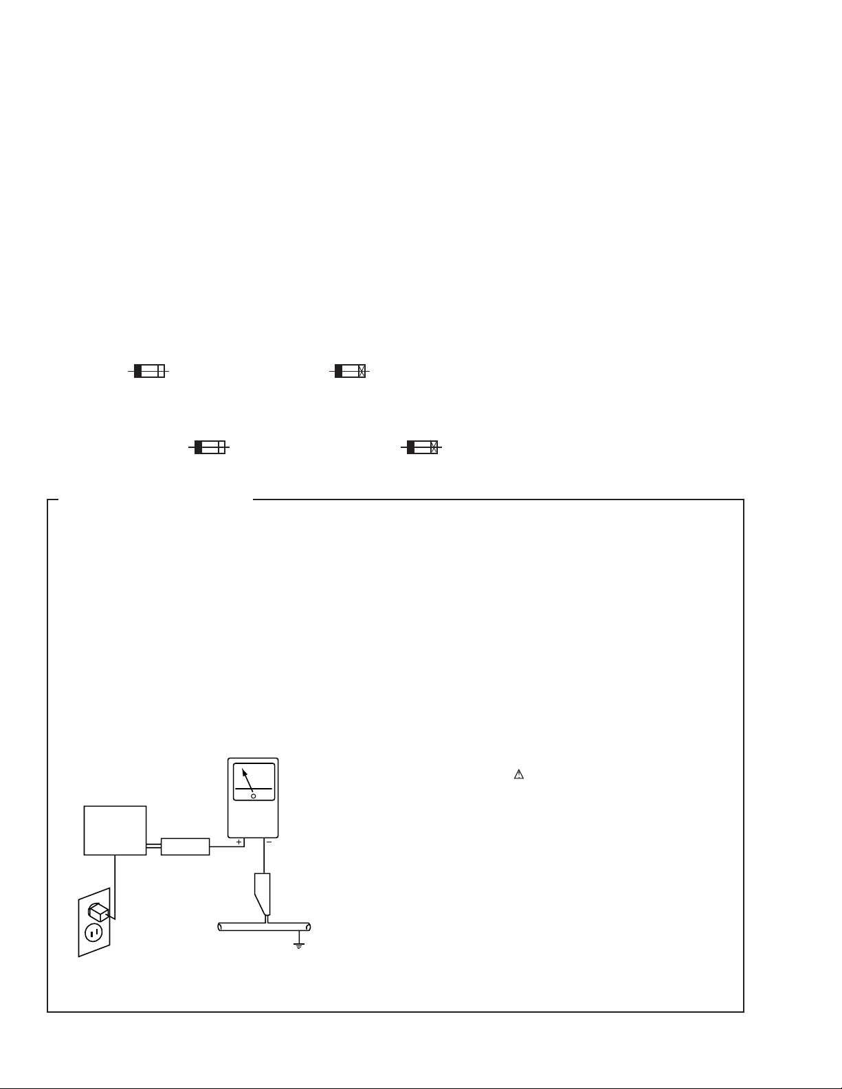
1. SAFETY PRECAUTIONS
The following check should be performed for the
continued protection of the customer and service
technician.
LEAKAGE CURRENT CHECK
Measure leakage current to a known earth ground (water
pipe, conduit, etc.) by connecting a leakage current tester
such as Simpson Model 229-2 or equivalent between the
earth ground and all exposed metal parts of the appliance
(input/output terminals, screwheads, metal overlays, control
shaft, etc.). Plug the AC line cord of the appliance directly
into a 120V AC 60Hz outlet and turn the AC power switch
on. Any current measured must not exceed 0.5mA.
Reading should
not be above
0.5mA
Earth
ground
Device
under
test
Also test with
plug reversed
(Using AC adapter
plug as required)
Leakage
current
tester
Test all
exposed metal
surfaces
ANY MEASUREMENTS NOT WITHIN THE LIMITS
OUTLINED ABOVE ARE INDICATIVE OF A POTENTIAL
SHOCK HAZARD AND MUST BE CORRECTED BEFORE
RETURNING THE APPLIANCE TO THE CUSTOMER.
2. PRODUCT SAFETY NOTICE
Many electrical and mechanical parts in the appliance
have special safety related characteristics. These are
often not evident from visual inspection nor the protection
afforded by them necessarily can be obtained by using
replacement components rated for voltage, wattage, etc.
Replacement parts which have these special safety
characteristics are identified in this Service Manual.
Electrical components having such features are identified
by marking with a
in this Service Manual.
The use of a substitute replacement component which does
not have the same safety characteristics as the PIONEER
recommended replacement one, shown in the parts list in
this Service Manual, may create shock, fire, or other hazards.
Product Safety is continuously under review and new
instructions are issued from time to time. For the latest
information, always consult the current PIONEER Service
Manual. A subscription to, or additional copies of, PIONEER
Service Manual may be obtained at a nominal charge from
PIONEER.
on the schematics and on the parts list
AC Leakage Test
2
Page 3
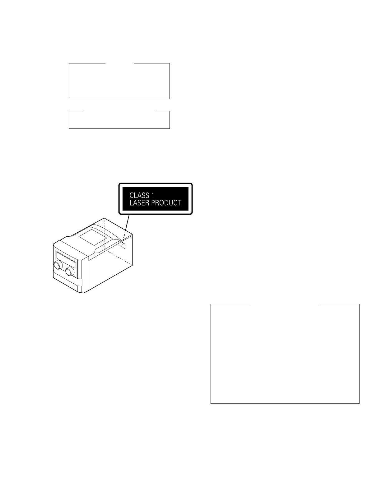
IMPORTANT
THIS PIONEER APPARATUS CONTAINS
LASER OF CLASS 1.
SERVICING OPERATION OF THE APPARATUS
SHOULD BE DONE BY A SPECIALLY
INSTRUCTED PERSON.
LASER DIODE CHARACTERISTICS
MAXIMUM OUTPUT POWER: 5 mW
WAVELENGTH: 760 - 800 nm
LABEL CHECK (For MYXCN and NVXCN Types)
XR-MT3
Additional Laser Caution
1.Laser Interlock Mechanism
The position of the switch for detecting loading state is
detected by the system microprocessor, and the design
prevents laser diode oscillation when the switch is pressed
physically.
Thus, the interlock will no longer function if the switch is released
physically and deliberatery .
Laser diode oscillation will continue, if pin 46 of TA2065F (IC2)
on the CD SERVO PCB ASSY is connected to GND, or else
the terminals of Q1 are shorted to each other (fault condition).
2.When the cover is opened, close viewing of the objective
lens with the naked eye will cause exposure to a Class 1
laser beam.
3
Page 4
XR-MT3
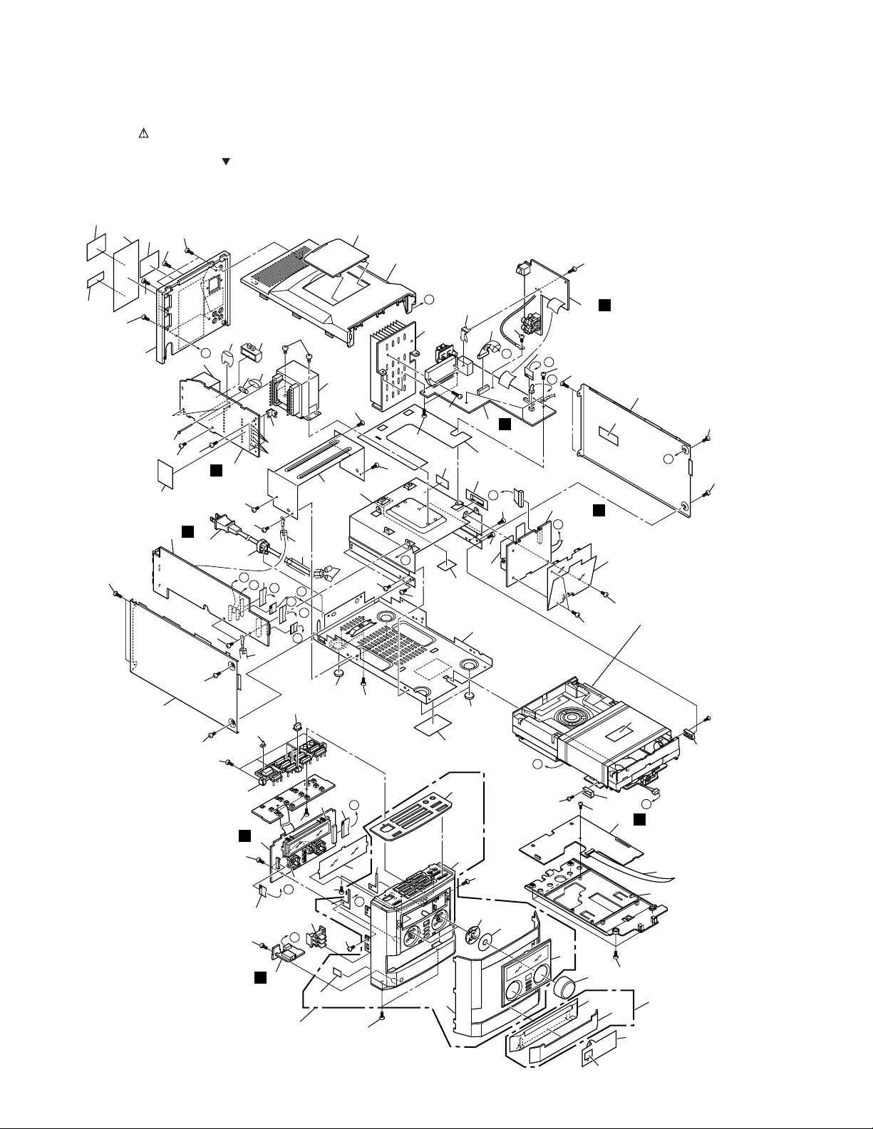
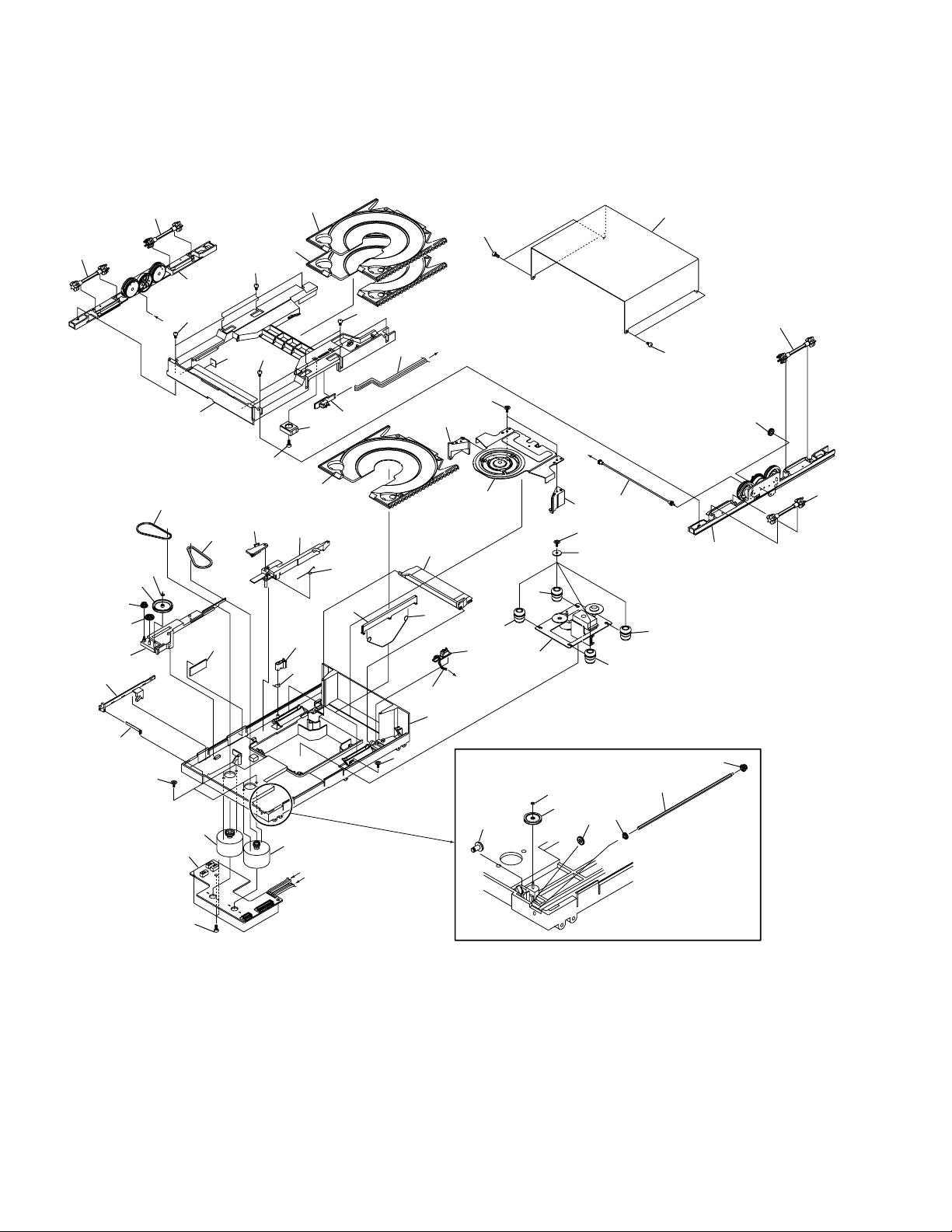
2. EXPLODED VIEWS AND PARTS LIST
NOTES:• Parts marked by "NSP" are generally unavailable because they are not in our Master Spare Parts List.
The mark found on some component parts indicates the importance of the safety factor of the part.
•
Therefore, when replacing, be sure to use parts of identical designation.
Screws adjacent to mark on the product are used for disassembly.
•
2.1 EXTERIOR SECTION
69
70
71
8
8
87
34
8
89
15
K
44
54
9
72
A
6
68
78
93
2
22
H
4
77
57
73
62
52
50
9
80
59
55
1
C
G
15
6
J
95
E
2
F
18(2/2)
H
6
79
14
D
8
49
8
45
81
66
E
53
2
33
Refer to section
"2.2 CD MECHA.
SECTION".
85
39
82
10
I
B
21
41
8
17
60
6
8
K
16
40
8
16
36
8
84
48
65
20
26,61
2
A
8
16
63
B
29
E
18(1/2)
7
15
32
64
G
F
2
8
37
8
47
G
12
8
23
8
88
38
90
F
25
28
31
13
44
J
5
27
7
56
51
91
92
94
B
E
D
C
35
42
8
43
C
75
46
I
76
19
15
62
2
24
D
74
58
8
A
9
16
67
4
Page 5

(1) EXTERIOR SECTION PARTS LIST
XR-MT3
Mark No. Description Part No.
1 AMP PCB Assy AUD-PMT1E
2 Screw BBZ30P060FMC
3 Screw KBZ30P060FNI
4 Screw BBZ30P140FMC
5 Screw BBZ40P060FMC
6 Screw BPZ20P050FMC
7 Screw BPZ26P080FMC
8 Screw BPZ30P100FNI
9 Screw CBZ30P060FMC
10 CD SERVO PCB Assy CD--PMT1E
11 • • • • • •
12 DISPLAY PCB Assy See Contrast table(2)
NSP 13 HP JACK PCB Assy • • • • • •
14 TERMINAL/JACK PCB Assy JK--PMT1E
15 Screw KBZ30P040FMC
16 Screw KBZ30P060FNI
17 CD DOOR Assy MT SUBPMT1DR01
18 POWER PCB Assy See Contrast table(2)
19 S-Assy PMT1 FP01 See Contrast table(2)
19 S-Assy PMT1 FP02 See Contrast table(2)
20 TUNER PCB Assy See Contrast table(2)
21 FFC Cable 16Pin 040160100101
22 FFC Cable 16Pin 040160260100
23 FFC Cable 17Pin 040170100100
24 FFC Cable 24Pin 040240200130
25 FFC Cable 30Pin 040300400100
26 Power TF EI35 120V See Contrast table(2)
26 Power TF EI35 230V See Contrast table(2)
26 Power TF EI35 11-2 See Contrast table(2)
27 Power TF EI66 120V See Contrast table(2)
Mark No. Description Part No.
47 Direct Access Knob Set 510PMT109010
48 Side Panel-L 600PMT117001
49 Side Panel-R 600PMT118001
NSP 50 Bottom Tray 600PMT121000
51 Transformer Bracket 605PMT122000
52 FCC Cable HLD 605PMT142000
53 Cable Holder 605PMT143000
54 Power Heat Sink 613PMT124000
55 Heat Sink 613PMT131000
56 CD Shield Plate 650PMT139000
57 CD Insulation Sheet 650PMT144000
58 Display Filter Plate See Contrast table(2)
59 PC Sheet 650PMT149000
60 Transport Stopper PL 650PMT197010
61 Shielding Plate 650277225000
62 Rubber Foot 700PMT130000
63 Capacitor Boot 700PMT150000
64 Bushing See Contrast table(2)
65 Cable/Plastic Tie 727000100000
66 65 Label See Contrast table(2)
NSP 67 Trans. Stopper Label 809PMT194021
68 FCC Label See Contrast table(2)
NSP 69 Serial No Barcode Label See Contrast table(2)
70 Warning Label MT3KUC See Contrast table(2)
70 Warning Label MT3E See Contrast table(2)
70 Warning Label MT3D See Contrast table(2)
70 Warning Label MT3DL See Contrast table(2)
71 Back Label MT3KUC See Contrast table(2)
71 Back Label MT3MY See Contrast table(2)
71 Back Label MT3NV See Contrast table(2)
27 Power TF EI66 230V See Contrast table(2)
27 Power TF EI66 11-2 See Contrast table(2)
28 Micro Fuse 251001 124010010002
29 Fuse #23901.6 (1.6A) See Contrast table(2)
29 Fuse #21801.6 (1.6A) See Contrast table(2)
30 Micro Fuse 251002 124020010002
31 Micro Fuse #25103.5 124035010000
32 PLA-ULP-6’06"-SP2NMG See Contrast table(2)
32 PLA-VDE-6’06"-VDG See Contrast table(2)
32 PLA-MOU-6’06"-BS6 See Contrast table(2)
32 PLA-JIS-6’06"-JIS See Contrast table(2)
33 CD MECHA,CMCJ 153000117000
34 Top Panel See Contrast table(2)
35 Direct Access Knob Lens 500PMT111000
36 Back Cover See Contrast table(2)
37 Power Standby Lens 500PMT129000
38 Fuse Insulation Cap 500623200000
39 CD Base Adaptor R 503PMT125000
40 CD Base Adaptor L 503PMT126000
41 Servo PCB Bracket 505PMT114000
42 FL Bracket 505PMT134000
43 LED Bracket 505PMT135000
44 PCB Mounting Bracket 505PMT136000
45 Volume Knob 510PMT103001
46 Clock Control Knob Set 510PMT108001
71 Back Label MT3DBD See Contrast table(2)
71 Back Label MT3DL See Contrast table(2)
72 Fuse Caution Label See Contrast table(2)
NSP 73 Front Panel 500PMT101001
NSP 74 GND. Copper Plate C 650PMT152000
NSP 75 GND. Copper Plate D 650PMT153000
NSP 76 GND. Copper Plate E 650PMT155000
NSP 77 Control Panel Plate 650PMT116010
NSP 78 Front Cover See Contrast table(2)
NSP 79 Display Lens 500PMT106010
NSP 80 Illuminated Ring 509PMT105000
NSP 81 CD Door 500PMT102001
NSP 82 CD Door Cover 600PMT120010
83 • • • • • •
84 PCB Insulation Sheet 650PMT157000
85 CD Caution Label See Contrast table(2)
NSP 86 Fuse Label See Contrast table(2)
87 Voltage Sel. Cover See Contrast table(2)
88 Voltage Sel. Knob See Contrast table(2)
NSP 89 Serial Label See Contrast table(2)
90 Tube AWG5 D4.72 L70 728000047L07
91 Tube AWG5 D4.72 L90 728000047L09
92 Tube AWG1 D7.35 L120 728000073L12
93 Tube AWG1 D7.35 L160 728000073L16
94 Tube AWG1 D7.35 L15 728000073L15
95 Ref Silver Label See Contrast table(2)
5
Page 6
XR-MT3
(2) CONTRAST TABLE
XR-MT3/KUCXCN, MYXCN, NVXCN, DBDXCN and DLXCN/NC are constructed the same except for the following :
Mark No. Symbol and Description
12 DISPLAY PCB Assy DIP-PMT1E DIP-PMT1E-E DIP-PMT1E-E DIP-PMT1E-DL DIP-PMT1E-DL
18 POWER PCB Assy GEN-PMT1E-UL GEN-PMT1E-GA GEN-PMT1E-GA GEN-PMT1E-DL GEN-PMT1E-DL
19 S-Assy PMT1 FP01 SUBPMT1FP01 Not used Not used SUBPMT1FP01 SUBPMT1FP01
19 S-Assy PMT1 FP02 Not used SUBPMT1FP02 SUBPMT1FP02 Not used Not used
20 TUNER PCB Assy TUN-PMT1E-UL TUN-PMT1E-EU TUN-PMT1E-EU TUN-PMT1E-DL TUN-PMT1E-DL
26 Power TF EI35 120V 123113513020 Not used Not used Not used Not used
26 Power TF EI35 230V Not used 123183513140 123183513140 Not used Not used
26 Power TF EI35 11-2 Not used Not used Not used 1231D3513140 1231D3513140
27 Power TF EI66 120V 123516636021 Not used Not used Not used Not used
27 Power TF EI66 230V Not used 123586636142 123586636142 Not used Not used
27 Power TF EI66 11-2 Not used Not used Not used 1235D6636140 1235D6636140
29 Fuse #23901.6 (1.6A) 124016020001 Not used Not used Not used Not used
29 Fuse #21801.6 (1.6A) Not used 124016000002 124016000002 124016000002 124016000002
32 PLA-ULP-6'06"-SP2NMG 134117120108 Not used Not used Not used Not used
32 PLA-VDE-6'06"-VDG Not used 134220120001 Not used Not used 134220120001
32 PLA-MOU-6'06"-BS6 Not used Not used 134240120014 Not used Not used
32 PLA-JIS-6'06"-JIS Not used Not used Not used 134100120001 Not used
34 Top Panel 500PMT104001 500PMT104001 500PMT104001 500PMT148001 500PMT148001
36 Back Cover 500PMT113001 500PMT181000 500PMT181000 500PMT113001 500PMT113001
58 Display Filter Plate 650PMT147001 650PMT147002 650PMT147002 650PMT147002 650PMT147002
64 Bushing 700PMT156000 700PMT146000 700PMT146000 700PMT146000 700PMT146000
66 65 Label 809PMT194010 Not used Not used Not used Not used
68 FCC Label 809PMT194030 Not used Not used Not used Not used
NSP 69 Serial No Barcode Label 809PMT194040 809PMT194120 809PMT194090 Not used Not used
70 Warning Label MT3KUC 809PMT194050 Not used Not used Not used Not used
KUCXCN MYXCN NVXCN DBDXCN DLXCN/NC
Part No.
70 Warning Label MT3E Not used 809PMT194080 809PMT194080 Not used Not used
70 Warning Label MT3D Not used Not used Not used 809PMT194100 Not used
70 Warning Label MT3DL Not used Not used Not used Not used 809PMT194110
71 Back Label MT3KUC 809PMT196010 Not used Not used Not used Not used
71 Back Label MT3MY Not used 809PMT196020 Not used Not used Not used
71 Back Label MT3NV Not used Not used 809PMT196030 Not used Not used
71 Back Label MT3DBD Not used Not used Not used 809PMT196040 Not used
71 Back Label MT3DL Not used Not used Not used Not used 809PMT196050
72 Fuse Caution Label 809036380130 Not used Not used Not used Not used
NSP 78 Front Cover 600PMT119010 600PMT119020 600PMT119020 600PMT119010 600PMT119010
85 CD Caution Label Not used 809PMT194070 809PMT194070 809PMT194070 809PMT194070
NSP 86 Fuse Label Not used 809PMT194130 809PMT194130 809PMT194130 809PMT194130
87 Voltage Sel. Cover Not used Not used Not used 500PMT110001 500PMT110001
88 Voltage Sel. Knob Not used Not used Not used 510PMT112001 510PMT112001
NSP 89 Serial Label Not used Not used Not used 809000009000 809000009000
95 Ref Silver Label Not used 809PMT151000 809PMT151000 Not used Not used
6
Page 7

XR-MT3
7
Page 8
XR-MT3
2.2 CD MECHA. SECTION
41
23
21
33
6
42
43
34
46
28
51
56
57
27
32
1
A
20
49
53
C
18
38
39
45
B
40
19
5
53
52
39
8
8
3
50
C
2
36
48
29
25
26
22
11
35
47
37
51
50
55
24
9
8
49
7
8
4
38
15
54
44
49
31
30
B
A
53
16
48
17
14
13
10
12
8
Page 9

CD MECHA. SECTION PARTS LIST
•
XR-MT3
Mark No. Description Part No.
1 Assy Chassis 45-093-4256
2 Drawer 2 45-264-3278
3 Assy Holder L 45-093-3241
4 Assy Holder R3B 45-093-3296
5 Assy Gear Drive 45-093-4243
6 Assy Carriage 101 45-093-4347
7 Bevel Gear 4 45-222-4214
8 Assy Gear Star 45-093-4244
9 Cover 2 45-112-3154
10 Shaft 45-300-4173
11 Slider 4 45-259-3175
12 Gear Spline 45-222-4021
13 Bevel Gear 1 45-222-4059
14 Gear Idler 1 45-222-4176
15 Plate Spring 45-160-4174
16 Bevel Gear 3 45-222-4177
17 Pulley C 45-222-4058
18 Assy Clamper SO 45-093-4358
19 Arm Slider R 45-219-3187
20 Arm Slider L 45-219-3188
21 Slider 1 45-259-2185
22 Assy Slider 2 45-093-3240
23 Arm Stopper A2 45-239-4279
24 Arm Stopper B 45-239-4065
25 Gear Idler A 45-222-4128
26 Gear Idler C 45-222-4051
27 Lever 2 45-259-3289
28 Lifter 45-259-3025
29 Pulley A 45-229-4052
30 Assy Motor CRG S 45-093-4238
Mark No. Description Part No.
31 Assy Motor DRW S 45-093-4239
32 Spring 01-080-4541
33 Spring 01-082-4643
34 Spring 01-082-4647
35 Belt 02-083-4171
36 Belt 02-083-4172
37 Cushion 45-063-4136
38 Insulator 45-063-3201
39 Insulator 45-063-3202
40 Pickup Unit KSM213CCM
41 Assy Carriage 201 45-093-4348
42 Assy Carriage 301 45-093-4349
43 Spacer SW 45-219-4127
44 Assy PC Board A 45-093-4263
45 Assy PC Board B 45-093-4265
46 Assy PC Board C 45-093-4264
47 Rubber Cushion 45-063-4115
48 Washer GWP15×045025S
49 Screw GSL20A2606
50 Screw GSL20B2006
51 Screw GSL10B2006
52 Washer GWN31×120050
53 Screw GSL15A2608
54 Screw GSP14A2604
55 Screw GST15A2005
56 Lead Wire 45-072-4171
57 Lead Wire 45-072-4172
9
Page 10
1
23
XR-MT3
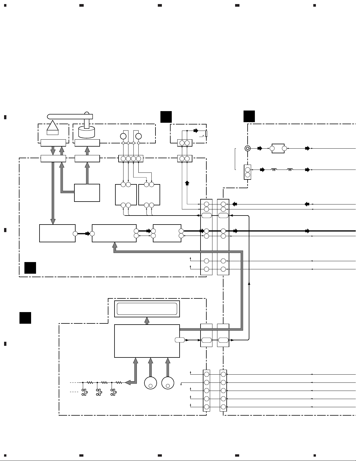
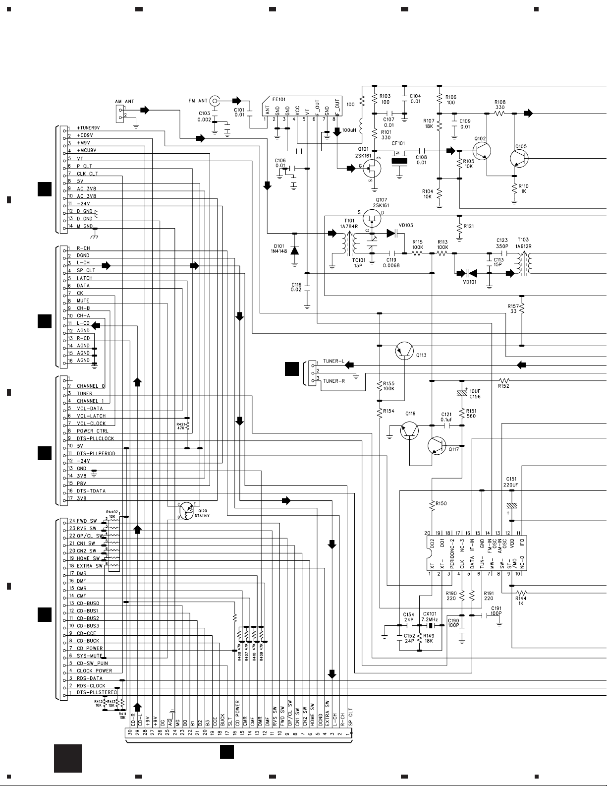
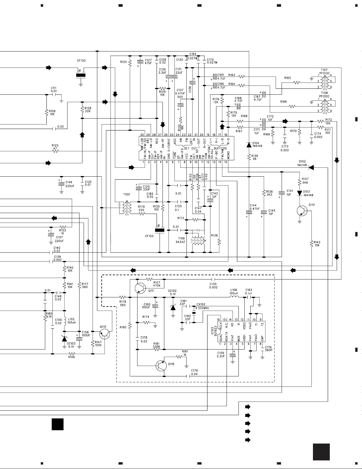
3. BLOCK DIAGRAM AND SCHEMATIC DIAGRAM
A
3.1 BLOCK DIAGRAM
4
HP JACK PCB ASSY
7 3
IC7
FIN
RIN
2
6
BA4558N
F
IC4
CN1
(4P)
(PH)
PHONES
14
CN204
(4P)
ANTENNA
(PH)
CN6
(30P)
L-CH
2
R-CH
5
12-1512-15
CD-L
1
7
CD-R
29
30
29
30
2
5
CN8
(30P)
FM
AM
PICKUP
ASSY
(16P)
CN3
(16P)
Spindle
Motor
CN4
(6P)
B
IC3
TA2092N
DRIVER
IC2
TA2065F
RF AMP.
RFO RFI
1
53
TC9284BF
DECODER
Carriage
Motor
IC1
-
M M
+
TA7291S
DRIVER
-
Drawer
Motor
+
4
321 14
CN5
CARR-
DRAW-
CARR+
DRAW+
7 3
IC6
TA7291S
RIN
LO
RO
DRIVER
6
2
9 1 9 1
FIN
CD MECHA.
TUNER PCB ASSY
A
(FM)
(AM)
FE101
1 8
T101 T103
CN102
CN101
1
2
(FM)
(AM)
(PH)(PH)
CONTROL DATA
+9V
27
27
28
28
CD SERVO PCB ASSY
B
+9V
C
LCD401
FL TUBE
DISPLAY PCB ASSY
G
CN401
(24P)
CN205
(24P)
CN402
IC401
PDA068A
73-76
8-10 8-10
SYSTEM CONTROL IC
CN404
(17P)
5V
10 10
12 12
3V8
-24V
FUNCTION
D
KEY INPUT
JOG
VOL
JOG
P8V
3V8
14 14
15 15
17 17
CN207
(17P)
10
1234
Page 11
(FM)
(AM)
FM-IN
1
IC101
LA1837NZ
AM-RF
27
TUNER-L
TUNER-R
5
17
16
+TUNER9V
CN13
(3P)
TUNER-L
TUNER-R
CN206
(16P)
L-CH
R-CH
L-CD
R-CD
CN11
(14P)
678
XR-MT3
A
: AUDIO SIGNAL ROUTE (RF/CD)
(T)
: AUDIO SIGNAL ROUTE (TUNER)
(AM)
: AUDIO SIGNAL ROUTE (AM)
(FM)
: AUDIO SIGNAL ROUTE (FM)
(AU)
: AUDIO SIGNAL ROUTE (AUX)
(PH)
: AUDIO SIGNAL ROUTE (PHONES)
TERMINAL/JACK PCB ASSY
D
(PH)
IC901
BA4558N
BUFFER
(AU)
CN206
(4P)
141
1.6A/250V
(AU)
SN206
(4P)
4
F306
L
AUXOUT
R
L
AUXIN
R
LIVE
NEUTRAL
L
SPEAKER
OUT
R
AC IN
B
C
D
12
13
10
SN302
1
2
3
5
6
8
9
10
7
9
(12P)
J201
(13P)
(AU)(AU)
7
9
(AU)(AU)
12
13
10
(PH)(PH)(PH)(PH)
18 1331 24
1 10
IC251
STK4142
AMPLIFIER
IC304
IC303
IC305
IC306
IC307
IC308
5 7
3 1
9V
TF302
POWER
TRANSFORMER
TF303
POWER
TRANSFORMER
(AU)
(AU)
32
IC201
CN302
AC31V
AC31V
AC24V
AC3.8V
MCUAC
CN203
9V
BH3854AFS
(12P)
1
2
3
5
6
8
9
10
(13P)
IC202
2 9
CN208
1
1
3
3
CN202
3
3
1
1
11
11
13
13
1
1
2
2
3
3
4
4
8
8
9
9
10
10
11
11
CN301
C
(3P)
AMP PCB ASSY
(T)(T)
(T)
(16P)
(AU)
(T)
14
15 13
(AU)
4
5
11
BU4052BC
9V +31V
CN204
(9P)
SN204
(9P)
9V
+TUNER9V
+M9V
+CD9V
+MCU9V
5V
AC3.8V AC3.8V
AC3.8V
-24V
(14P)
POWER PCB ASSY
E
+31V
9V
IC301
9V REG.
D312
5V
3 1
IC302
5V REG.
-31V
973
973
-31V
D301-D304
4 2
SELECTOR
11
5
6
7
8
Page 12
1
XR-MT3
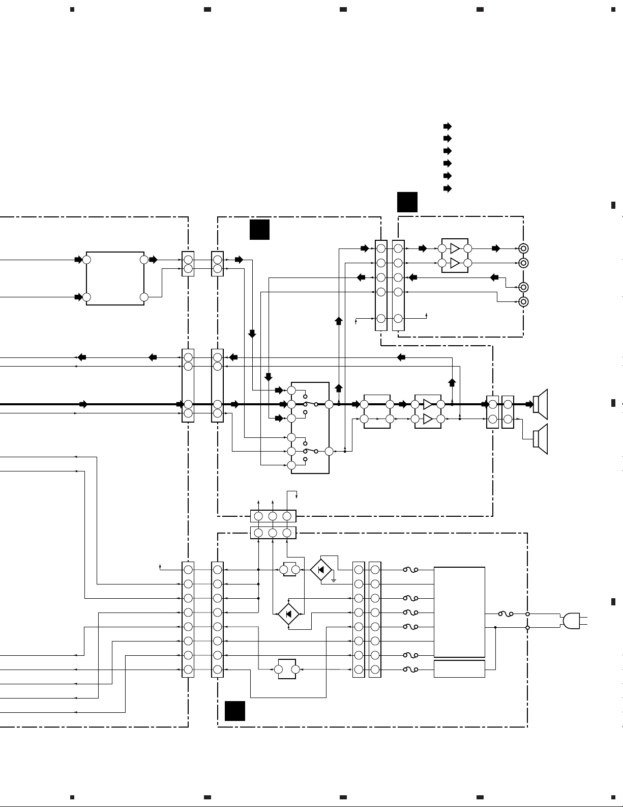
3.2 OVERALL WIRING DIAGRAM
A
PICKUP ASSY
23
4
HP JACK PCB
ASSY
B
F
CARRIAGE
MOTOR
DRAWER
MOTOR
CD
MECHA.
1 2 3 4 5 6 7 8 9 10 11 12 13 14 15 16
1 2 1 23 4 5 6 7 8 9
10 11 12 13 14 15 16
CN3
CN1CN204
DGND
1
1
2
2
R-CH
3
3
L-CH
4
4
S- CLT
CN5
CARR+
1
M
2
CARR-
3
DRAW-
4
M
DRAW+
CN4
DM+
1
2
DM-
3
FM+
4
FM-
5
SLT
6
GND
CN2
EXTRA SW
1
2
HOME SW
3
COM
4
CN2 SW
5
CN1 SW
6
OP/CL SW
7
FWD SW
8
RVS SW
CD SERVO PCB ASSY
B
(CD--PMT1E)
CN6 CN8
DGND
R-CH
L-CH
EXTRA SW
SP CLT
HOME SW
CN2 SW
CN1 SW
OP/CL SW
FWD SW
RVS SW
DMF
DMR
CMF
CMR
CD POWER
SLT
BUCK
CCE
B3
B2
B1
B0
MG
AG
DG
+9V
+9V
CD-L
CD-R
1
1
2
2
3
3
4
4
5
5
6
6
7
7
8
8
9
9
10
10
11
11
12
12
13
13
14
14
15
15
16
16
17
17
18
18
19
19
20
20
A
21
21
22
22
TUNER PCB ASSY
23
23
(KUCXCN : TUN-PMT1E-UL)
24
24
25
25
(MYXCN, NVXCN :
26
26
TUN-PMT1E-EU)
27
27
28
28
(DBDXCN, DLXCN/NC :
29
29
TUN-PMT1E-DL)
30
30
AM ANT FM ANT
1 2
CN101
FM ANT
CN102
KUCXCN
DBDXCN
DLXCN/NC
CN102
MYXCN
NVXCN
CN401 CN205
FWD SW
C
G
DISPLAY PCB
ASSY
(KUCXCN : DIP-PMT1E)
D
(MYXCN, NVXCN : DIP-PMT1E-E)
RVS SW
OP/CL SW
CN1 SW
CN2 SW
HOM SW
EXTRA SW
CD-BUS0
CD-BUS1
CD-BUS2
CD-BUS3
CD-CCE
CD-BUCK
CD POWER
SYS-MUTE
CD-SW PUIN
CLOCK POWER
RDS-DATA
RDS-CLOCK
DTS-PLLSTEREO
(DBDXCN, DLXCN/NC : DIP-PMT1E-DL)
DMR
DMF
CMR
CMF
24
24
23
23
22
22
21
21
20
20
19
19
18
18
17
17
16
16
15
15
14
14
13
13
12
12
11
11
10
10
9
9
8
8
7
7
6
6
5
5
4
4
3
3
2
2
1
1
NC
CHANNEL 0
TUNER
CHANNEL 1
VOL-DATA
VOL-LATCH
VOL-CLOCK
POWER CTRL
DTS-PLLCLOCK
5V
DTS-PLLPERIOD
-24V
GND
3V8
P8V
1 2 3 4 5 6 7 8 9 10 11 12 13 14 15 16 17
1 2 3 4 5 6 7 8 9 10 11 12 13 14 15 16 17
DTS-TDATA
3V8
CN207
CN404
12
1234
Page 13
5
678
XR-MT3
Note : When ordering service parts, be sure to refer to "EXPLODED VIEWS and PARTS LIST" or "PCB PARTS LIST".
L
CN13
TUNER-L
GND
TUNER-R
AUX IN
R
AUX OUT
L
R
CN203
CN201
1
1
2
2
3
3
TERMINAL/JACK PCB ASSY
D
(JK--PMT1E)
J201
1 2 3 4 5 6 7 8 9 10 11 12 13
1 2 3 4 5 6 7 8 9 10 11 12 13
LINEOUTL
MUTE CLT
LINEOUTR
+9V
SPCTL
AUXINL
AUXINR
MUTE
AGND
AGND
VOLOUTL
VOLOUTR
AGND
CN206
SUBWOOFER
1
1
2
2
3
3
4
4
L
SPEAKER
R
A
B
CN206 CN202
R-CH
1
L-CH
DATA
CK
CH-B
CH-A
L-CD
R-CD
1
2
2
3
3
4
4
5
5
6
6
7
7
8
8
9
9
10
10
11
11
12
12
13
13
14
14
15
15
16
16
DGND
SP CLT
LATCH
MUTE
AGND
AGND
AGND
AGND
CN11 CN301
+TUNER9V
1
1
+M9V
2
2
+CD9V
3
3
+MCU9V
4
4
VT
5
5
POWER CLT
6
6
CLOCK CLT
7
7
5V
8
8
AC3.8
9
9
AC3.8
10
10
-24V
11
11
D GND
12
12
D GND
13
13
M GND
14
14
AMP PCB ASSY
C
(AUD-PMT1E)
CN204
SN204
PWR CTLAC9V
AGND
GND
DGND
+3V
1 2 3 4 5 6 7 8 9
1 2 3 4 5 6 7 8 9
PGND
-31V
E
POWER PCB ASSY
(KUCXCN : GEN-PMT1E-UL)
(MYXCN : GEN-PMT1E-GA)
(NVXCN : GEN-PMT1E-GA)
(DBDXCN : GEN-PMT1E-DL)
(DLXCN/NC : GEN-PMT1E-DL)
MCUACGND
CN302 SN302
1
AC12V
AC12V
AC31V
AC31VGND
AC31V
AC24V
AC24VGND
AC3.8V
AC3.8V
MCUAC
RELAYB+
1
2
2
3
3
4
4
5
5
6
6
7
7
8
8
9
9
10
10
11
11
12
12
LIVE
NEUTRAL
C
AC IN
D
13
5
6
7
8
Page 14
1
XR-MT3
3.3 TUNER PCB ASSY
CN101
A
CN11
136-14PMT1-B00J
118-040102-002A
CN301
E
CN206 135-006116-160J
(AM)
23
CN102
KUCXCN, DBDXCN, DLXCN/NC : 118-040102-002A
MYXCN, NVXCN : 118-030401-000A
(FM)
C184
(AM)
50P
042-104511-000A
C180
0.01
(AM)
C288
50P
012-007840-010A
(AM)
(FM)
R412
L108
019-000107-006A
(FM)
KV1561A-2
(FM)
2.2K
4
(FM)
008-314170-008A
008-314170-008A
012-006120-010A
(HP)(HP)
007-200610-000A
(AM)
KV1561A-2
(AM)
B
CN202
C
CN13
CN207 135-TOCB17-171J
136-03PMT1-B00J
C
008-685500-000A
CN201
(HP) (HP)
4.7K
2SC1815
CN404
G
C
135-FEBTVK-240J
CN205
(HP)
IC102
010-849257-001A
(TC9257P)
2SC1815
2.2K
(T)(T)
8.2K
CN401
G
R424
2.2K
(HP) (HP)
009-607200-000A
D
CN8
B
CN6
14
135-006232-300J
A
1234
Page 15
5
678
XR-MT3
(AM)
C128
(T)
019-000107-006A
(AM)
(FM)(FM)
(AM)
6.8K
(FM)
IC101
010-101837-060A
(LA1837L)
(FM)
012-002240-010A
(AM)
C285
560P
C284
4.7K
4.7/50
012-000120-010A
5.6K
5.6K
2.2K
(T)
2.2K
5.6K
(T)
3.3K
3.3K
012-000120-010A
5.6K
(T)(T)
A
B
2SC1815
C282
011-010051-120A
A
019-000450-012A
(T)
018-010014-000A
4.7K
MYXCN, NVXCN
008-685500-000A
2.2K
008-618150-000A
2.2K
008-618150-000A
012-7NF803-0007A
009-604332-000A
ONLY
TUNER PCB ASSY
(KUCXCN : TUN-PMT1E-UL)
(MYXCN, NVXCN : TUN-PMT1E-EU)
(DBDXCN, DLXCN/NC : TUN-PMT1E-DL)
5
6
5.6K
: AUDIO SIGNAL ROUTE (RF/CD)
(T)
: TUNER SIGNAL ROUTE
(AM)
: TUNER SIGNAL ROUTE (AM)
(FM)
: TUNER SIGNAL ROUTE (FM)
(HP)
: AUDIO SIGNAL ROUTE (PHONES)
7
(T)(T)(T)
C
D
A
15
8
Page 16
1
XR-MT3
3.4 CD SERVO PCB ASSY
A
BA4558N-HT
B
23
037-003534-100
020-001693-000A
IC1
010-849284-000A
(TC9284BF)
DECODER
4
2.2M
135-006232-301J
4.7K
4.7K
CN8
1.5M
A
008-680500-000A
C
2SB562
(HP)
CN204
F
136-045CD1-201J
2SC1815
CD MECHA.
C72
D
136-08PMT1-250J
16
B
C73
3.3K
4.7K 4.7K
3.3K
1234
Page 17
5
678
XR-MT3
A
CD SERVO PCB
008-68500-000A
018-010014-000A
B
ASSY
(CD--PMT1E)
100K
TSO
220K
EFO
1.8K
VREF
100K
0.047
RFO
IC2
010-832065-000A
(TA2065F)
RF AMP.
4.7K
2.2M
2.2K
2.2K
100K
CD
PICKUP
135-TOCA16-160A
B
C
M
M
136-04PMT1-250J
5
CARRIAGE
MOTOR
DRAWER
MOTOR
IC3
010-832092-000A
(TA2092N)
6
W11
10K
: AUDIO SIGNAL ROUTE (RF/CD)
(HP)
: AUDIO SIGNAL ROUTE (PHONES)
CD
MECHA
136-067238-205J
47K
D
B
7
8
17
Page 18
1
23
4
XR-MT3
3.5 AMP PCB, TERMINAL/JACK PCB, POWER PCB and HP JACK PCB ASSYS
CN13
A
A
136-03189D-200J
MTZJ4.7B
135-006116-160J
4.7/50
(T) (T)
A
CN206
(AU)
(HP)
008-801144-000A
DTC114ES
(HP)(HP)(HP)
MTZJ5.1B
MTZJ5.1B
SELECTOR
B
4.7/50
(AU)
(AU)(AU)
(AU)
MTZJ9.1B
(AU)
(AU)
CN203
050-140060-200J
008-801144-000A
100
010-400009-001A
008-685500-000A
IC301
(BA09ST)
011-010240-120A
AMP PCB ASSY
C
(AUD-PMT1E)
008-801144-000A
008-801144-000A
C
(AU)
(AU)
(AU)
(AU)
(AU)
BA4558N-HT
(AU)
(AU)
(AU)
(AU)
(AU)
(AU)
CN11
(AU)
D
BA4558N-HT
A
135-2001WS-140J
18
C D E
1234
TERMINAL/JACK PCB ASSY
D
(JK--PMT1E)
Page 19
5
678
XR-MT3
(HP)
MTZJ5.1B
IC251
010-554141-000A
(STK4132)
: AUDIO SIGNAL ROUTE (RF/CD)
(T)
: TUNER SIGNAL ROUTE
(HP)(HP)
(HP)
008-680500-000A
(AU)
(HP)
128-122125-000A
011-024001-00A
R300
: AUDIO SIGNAL ROUTE (AUX)
: AUDIO SIGNAL ROUTE (PHONES)
HP JACK PCB
F
ASSY
116-008020-000
CN1
B
135-2001WR-040J
118-000134-001A
018-010016-202A
018-010016-202A
A
PHONES
SPEAKER
B
D301-D304 : 011-025401-000A
D306,D307,D309-D311,D313 : 011-024001-000A
4700/16
011-010082-120A
2SC1815
+5V
REGULATOR
008-685500-000A
135-005267-090J
136-09PMT1-C00J
E
CN302
011-024001-000A
POWER PCB ASSY
(KUCXCN : GEN-PMT1E-UL) (MYXCN : GEN-PMT1E-GA)
(NVXCN : GEN-PMT1E-GA) (DBDXCN : GEN-PMT1E-DL)
(DLXCN/NC : GEN-PMT1E-DL)
050-120060-251J
SN302
011-024001-000A
124-010010-002A
124-035010-000A
124-035010-000A
124-010010-002A
124-010010-002A
019-500160-000A
128-090109-000A
LIVE
NEUTRAL
AC IN
C
D
• NOTE FOR FUSE REPLACEMENT
CAUTION -
5
FOR CONTINUED PROTECTION AGAINST RISK OF FIRE.
REPLACE WITH SAME TYPE AND RATINGS ONLY.
C E F
6
7
19
8
Page 20

1
XR-MT3
3.6 DISPLAY PCB ASSY
DISPLAY PCB
G
A
ASSY
(KUCXCN : DIP-PMT1E)
(MYXCN, NVXCN : DIP-PMT1E-E)
(DBDXCN, DLXCN/NC : DIP-PMT1E-DL)
23
LED401-LED403 : 110-033045-013A
1K
1K
4
B
1K
CN205
A
135-FESTVK-240J
C
For
DOWNLOAD
R135
NC
CN207
SW401-SW415 : 021-114165-000A
A
110-033040-013A
C501
D
135-TOCB17-171J
20
G
110-033045-013A
1234
Page 21

5
678
XR-MT3
IC401
LC87F65C8A-QIP
SYSTEM CONTROL IC
115-000920-000A
A
B
C
R462
1K
10K
111-000638-000A
020-000800-000A
009-332768-100A
DISPLAY PSB ASSY
S401 : STOP 7
S402 : PLAY 3 8
S403 : BASS/TREBLE
2SC1815
Q406
R461
100K
C500
5
6
KUCXCN,MYXCN,NVXCN
ONLY
KUCXCN,DBDXCN, DLXCN/NC
ONLY
KUCXCN
DBDXCN
DLXCN/NC
MYXCN
NVXCN
7
S404 : STANDBY/ON
S405 : ENTER
S406 : TIMER
S407 : DISPLAY/CLOCK
S408 : 4 / 1 / TUNING –
S409 : ¡ / ¢ / TUNING +
S410 : CD SELECT 3
S411 : CD SELECT 2
S412 : CD SELECT 1
S413 : CD3 OPEN/CLOSE 0
S414 : CD2 OPEN/CLOSE 0
S415 : CD1 OPEN/CLOSE 0
G
8
D
21
Page 22

1
23
XR-MT3
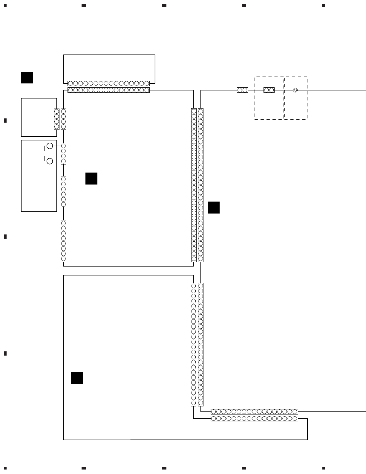
4. PCB CONNECTION DIAGRAM
NOTE FOR PCB DIAGRAMS :
A
Part numbers in PCB diagrams match those in the schematic
diagrams.
The parts mounted on this PCB include all necessary parts for
several destinations.
For further information for respective destinations, be sure to
check with the schematic diagram.
View point of PCB diagrams.
4
Connector
P.C.Board
B
4.1 TUNER PCB ASSY
H
CN401
C
R413
H
CN404
CN207
W242
3V8
5 VOL-DATA
6 VOL-LATCH
7 VOL-CLOCK
8 POWER CTL
9 DTS-CLOCK
10 6V
11 DTS-PERIOD
Capacitor
Chip Part
R411
R412
1
FWD SW
RVS SW
O/C SW
5
CN1 SW
CN2 SW
HOME SW
EXTRA SW
R421
10
DMR
DMF
CMR
1 NC
CMF
15
2 CH 0
CD-BUS0
3 TUNER
CD-BUS1
CD-BUS2
4 CH 1
CD-BUS3
CD-CCE
CD-BUCK
CD-POWER
SYS-MUTE
CD-SW_PUN
CLOCK-PWR
RDS-DATA
W120
RDS-CLOCK
DTS-STEREO
12 -24V
13 GND
14 3.8V
15 P8V
16 DTS-DATA
17 3.8V
B
20
15
10
CN6
CN205
SIDE A
SIDE B
W105
RA402
W101
5
+5V
W109
1
R408
TUNER PCB ASSY
A
CONTACT SIDE
CN8
1
W106
R407
W102
DGND
W107
W108
R410
R424
W111
M9V
R409
W110
MGND
W234
SPCLT
W104
A GND
W235
AGND
W240
DGND
R CH
L CH
CMR
W103
DGND
CN2
O/C
RVS
DMR
SLT
CCE
M 9V
5
15
B2
B0
25
W233
E
CD L
Q120
5 LATCH
E
W241
+5V
D GND
EXTRA
HOME
CN1
10
DMF
CMF
CD PWR
BUCK
B3
20
B1
M GND
D GND
CD 9V
CD R
30
1 HRCH
2 D GND
3 HLCH
4 SP CLT
CN206
FWD
W232
CD9V
10
6 DATA
CONTACT SIDE
7 CK
8 MUTE
9 CH B
10 CH A
11 CD L
12 A GND
13 CD R
14 A GND
R178
R161
W113
DZ102
L106
C163
C161
R199
C162
CX102
RED
1
5
MCU8V
W114
AGND
W117
15
W115
W119
W116
DGND
15 A GND
16 LINE MUTE
1
CN13
W141
CD9V
M9V
CD9V
M9V
MCU9V
UNREG+
P CLT
C CLT
5V
W118
DGND
10
10
15
W230
1
Q118
IC103
CN11
TU9V
E
R169
R147
C141
R157
C171
T108
C146
E
Q115
R137
T107
R139
C144
D104
R167
R138
R166
R165
C145
C142
R168
W124
AGND
W129
C167
R136
AGND
15
16
C196
C170
R175
R176
E
E
AGND
RED
W180
W127
W126
5
+5V
MGND
AC 3.8V
AC 3.8V
-24V
D GND
D GND
M GND
5
C160
C159
1
W122
R155
R142
AGND
E
UNREG+
W128
R181
C178
C176
W121
R160
C179
E
R154
R192
E
Q112
E
W123
R172
Q113
W130
AGND
D103
C174
C173
W131
W125
R171
C172
D102
R170
C
CN202
CN201
C
E
CN301
D
22
A
Q120
Q118
IC103
Q113
Q112
Q115
1234
Page 23

5
C
678
XR-MT3
A
B
C156
R101
R144
P105
WHITE
FE101
CF101
1051
E
Q101
C150
W133
E
R109
R180
R182
L107
E
R106
Q105
E
Q107
Q117
C121
E
R151
C105
W135
C104
C111
E
T103
R110
R108
R115
E
R121
VD103
C119
C182
PMT1-01-01
E
E
R107
C123
C120
C106
R105
P101
E
C102
Q116
E
C183
C103
E
VD101
C184
C101
C109
C113
C116
R113
W143
D101
CN102,
CN102
Q102
T101
TC101
CN101
SIDE A
C
D
C132
R124
W134
+9V
W138
W139
W140
C185
C154
W142
R179
R150
W226
R125
C152
R149
T105
R153C157
C139
W136
CX101
R141
R140
C148
20
R152
R177
L102
C180
R111
P104
IC102
W245
R146
C151
R103
R104
DZ103
R102
W247
15
C108
C107
C181
P102
P103
C158
WHITE
T106
C187
C168
252016
R129
C166
C137
C136
C188
5
R132
R163
R134
IC101
R133
R173
1
R128
C131
C130
30
C197
C135
W124
AGND
D104
144
R166
R165
R167
R138
C145
C142
R168
C167
R136
W129
AGND
C177
C196
15 10
C170
C169
R175
R176
C165
TUNER BOARD
C147
CF102
P106
R164
C133
C125
C190
C191
R130
W227
AGND
W246
C126
C128
C127
C129
C186
R127
R174
E
E
Q111
AGND
CF103
W132
+9V
C140
+9V
W243
R190
R191
IC101
Q111
IC102
5
6
Q101
Q105
Q107
Q102
7
A
8
23
Q116Q117
Page 24

1
23
XR-MT3
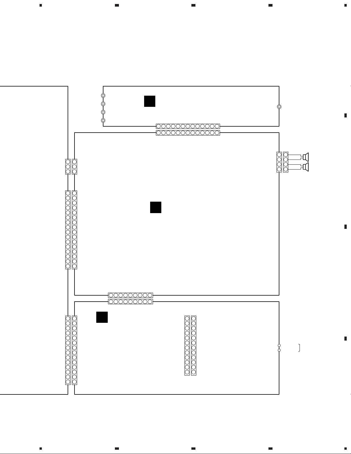
4.2 CD SERVO PCB and HP JACK PCB ASSYS
4
A
B
CARRIAGE
MOTOR,
DRAWER
MOTOR
C
1
RED
BLACK
CN1
CN5
W47
W48
1
SPCLT
IC5
C72
CD+9V
GNDM
5
IC6
R28
R33
OP/CL
51
HOME
COM
CN1
CN2
51
CN2
L-CH
DRAW+
DRAWCARRCARR+
1
RVS
FWD
R-CH
DGND
PMT-1-01-03
W45
W46
R67
W44
R68
EXTRA
RED
SPCLT
L-CH
DGND
CN2
EXTRA
HOME
R-CH
51015 2520 30
1
PICKUP
ASSY
C73
OP/CL
RVS
CD+9V
CMR
DMR
FWD
CMF
DMF
CN1
R60
R61
R59
R58
R57
R56
R35
CCE
SLT
CDPWR
W43
B2
W42
B0
B1B3BUCK
W41
CD+9V
GNDCD
R90
+9V
AG
DG
DG
VREF
W40
CDL
+9V
CDR
15
C75
Q5
1
5
C42
CN6
CN3
K19
CD+9V
CD MECHA.
VREF
W36
10
CD+5V
W37
GNDCD
W39
W38
C54
C51
K20
R93
Q6
R91
W49
R95
R94
SERVO BOARD
1
IC4
C56
W34
C49
R40
D2
R39
CD+9V
W35
5
GNDCD
R92
GNDCD
W33
D3
R41
C50
CD SERVO PCB ASSY
B
GND
SLT
FM-
FM+
DM-
DM+
C48
L1
R73
R72
C55
D1
W1
W2
W3
W4
W5
CD+5V
W30
CD+5V
W31
1
RED
CN4
5
W6
W7
TEO
C61
X1
C62
Q2
R38
K21
C35
W11
W19
C65
C47
W21
C68
R36
W12
VR3
Z1
GNDM
1
W13
VR2
GNDCD
W24
C46
L2
C40
C22
W8
CD+9V
W9
20 15
W14
C4
W15
TEB
C20
C16
C27
GNDCD
W25
TSO
W26
C37
C45
C41
C36
GNDM
105
3
2
W29
CD+5V
VREF
W17
R1
FEO
W23
C39
W20
W22
W10
IC3
1
C29
C31
W28
W32
Q1
R34
VR4
FEO
R2
W18
C12
GNDCD
CD+5V
GNDCD
GNDCD
4
C34
VR1
FEO
W16
GNDCD
RFO
W27
C38
C9
D
CD MECHA.
PMT1-01-10
24
B F
CN8
A
IC6 IC4Q5 Q6
IC5
VR3
VR2
IC3 Q1
VR1
VR4
F
L205
CN204
D261
HP JACK PCB ASSY
C280C281
D260
HP201
C287
1234
P201
HP BOARD
SIDE A
Page 25

1
GNDCD
GNDM
CD+9V
CD+9V
GNDCD
CD+9V
GNDCD
VREF
VREF
CD+5V
CD+9V
CD+9V GNDCD
GNDCD
CD+5V
CD+5V
CD+5V
GNDCD
GNDCD
GNDCD
GNDCD
GNDM
CD+9V
GNDM
CD+5V
GNDCD
SERVO BOARD
1
DGND
R-CH
L-CH
SPCLT
CDR
+9VDGDG
B3
B1
BUCK
CDPWR
CMF
DMF
FWD
CN1
HOME
EXTRA
R-CH
DGND
L-CH
SPCLT
CN2
OP/CL
RVS
DMR
CMR
SLT
CCE
B2B0AG
+9V
CDL
5
10
15
GND
SLT
FM-
FM+
DM-
DM+
51
10 5 1
15 20
5
1
30
25
20
15
10 5
5
1
EXTRA
HOME
COM
CN2
CN1
OP/CL
FWD
RVS
5
5
1
1
1
CARR+
CARR-
DRAW-
DRAW+
80757065
60 55 50 45
40
35
30
25
2015105
38
2415
1
48 45 40
353025
20
14 10
51
PMT-1-01-03
R32
R83
C26
C28
R30
R24
R31
R29
R27
R26
R25
C8
C43
C15
C1
R15
C17
C32
R17
C24
C44
R23
R22
R16
R6
C25
C2
IC2
C74
R37
C60 R53
C11
R3
C6C7
R5
C57
R48
R46
R55
C64
R45
R44
R43
R42
R51
R50
C14
R82
R75
R77
R74
R76
C30
R8
C23
C18
C69
C19
C13
C10
R10
R13
R11
R12
C21
R7
R21
R20
R19
IC1
R9
C33
C66
R66
C3
C71
R4
C59
R54
C58
C53
C52
R52
R47
R49
SIDE B
IC2
IC1
CD SERVO PCB ASSY
B
234
XR-MT3
A
B
C
D
B
1
2
3
4
25
Page 26

1
0
D
-31V
XR-MT3
4.3 AMP PCB ASSY
A
23
4
E
E
R291
E
R294
R293
Q261
R300
PWRCTRL
AC
9V
AGND
GND
+31V
PGND
-31V
C229
AGND
C260
Q258
E
Q264
1
W268
W211
E
Q260
E
R283
AGND
E
W280
CN2
5
W267
C278
E
E
E
Q259
E
E
R292
Q262
R228
B
W258
W259
AMP PCB ASSY
C
SN204
E
W291
R210
R206
R211
R202
C209
D201
C
C203
R215
C207
R204
R203
R214
15 10
C206
P4
C210
C204
C211
IC201
51
TUN-R
D256
AGND
TUN-L
D257
16
1
CN201
W203
HPRCH
PMT1-01-02
R218
R217
C215
Q201
E
E
W204
1
HPGND
HPLCH
HPGND
R209
5
SP-CLT
R208
CN202
CK
DATA
LATCH
R205
10
CH-B
MUTE
W206
CH-A
R219
C227
W207
D208
C213
C214
15
P1 CN203
AGND
CD-R
AGND
AGND
VIDEO
CD-L
C230
C228
IC202
R216
C217
C212
C218
C216
C219
C226
C220
C235
C223
C222
C221
R227
AUDIO BOARD
D209
R226
D203
C234
R224
R223
R222
R221
C232
C231
D202
D204
DGND
W290
C224
D206
C236
CN208
R225
R290
C237
D205
W252
W201
W209
W213
R220
C233
1
C225
Q257
Q263
R229
+9V
DGND
W214
W212
AGND
E
GND
W215
E
E
P3
W216
E
DGND
W228
CN13
A
IC201 Q201
D
26
C
CN206
A
Q262
Q257-Q259
Q263
Q264
Q260Q261
1234
Page 27

E
E
R291
E
E
R294
Q261
R300
PWRCTRL
AC
9V
AGND
GND
DGND
+31V
PGND
-31V
Q258
E
R293
Q264
1
W268
C229
C260
E
Q260
E
R283
E
W280
CN204
5
W267
D252
-31V
C262
C270
E
Q251
E
R249
W269
GNDB
GND
E
E
W288
5
C269
D251
Q265
C280
C263
R270
R250
C268
R269
R266
R267
R268
R282
R265
C261
E
Q253
E
C264
A3
Z6
C267
E
E
GND
Q252
C271
C259
R271
W287
R281
R272
R263
R279
W285
R287
678
XR-MT3
A
CN207
1
R254
R262
R278
R251
R280
R252
R257
D255
C255
C257
R258
W263
+31V
C251
D253
R255
C266
R264
-31V
W264
C265
R259
C252
C253
W257
R253
C279
R274
W286
R277
C256
R256
C258
R276
R261
R260
C254
R275
10
R273
5
IC251
15
1
1
618
12
L253
RL251
R295
C277
C276
B
C
16
15
9
W228
AGND
Q264
W211
Q260Q261
CN203
AGND
MUTE
Q265
Q251
AGND
VOLOUTR
AGND
VOLOUTL
D
5
AGND
AGND
W292
LINEOUTL
J201
SPCTL / GND
1051
LINEOUTR
+8V
SPCTL
Q253
Q252
AUXINR
P2
AUXINL
D254
VIDEO
W235
W289
W283
AGND
R288
C272
R296
E
E
E
E
R285
R286
R289
Q256
Q255
L201
CN206
SIDE A
D
C
6
7
8
27
Page 28

1
R
XR-MT3
4.4 POWER PCB ASSY
A
CN11
A
23
POWER PCB ASSY
E
4
PMT1-01-06
R304
R302
UNREG+
D312
GND
R306
AC31V
W305
C313
R307
R303
W316
D306
D310
UNREG+
Q302
E
E
IC301
+TUNER8V
+CD8V
C301
+M8V
+MCU8V
UNREG+
5
P CLT
CLK CLT
5V
B
P CLT
AC
+9V
A GND
D GND
S GND
+31V
POWER GND
-31V
W319
W315
R313
W302
1
5
+9V
+9V
+9V
W320
W321
10
+5V
W301
BROWN
SN204
C
RECTIFIER BOARD
M GND
+9V
W314
AC 3.8V
AC 3.8V
-24V
D GND
D GND
D313
W304
AC
1
UNREG+
CN301
C317
W318
C318
IC302
R312
C307
C302
D308
P301
Q301
E
C320
R305
E
D305
D309
W317
AC31V
W308
W313
C310
E
R310
GND
E
D301
Q303
C309
D307
W303
C308
D303
C305
C306
D304
D302
C304
C303
R309
E
W312
W311
AC3V8
AC3V8
RELAY B+
MCU AC GND
MCU AC
AC 3.8V
AC 3.8V
AC 24V GND
AC 31V GND
R311
W309
E
Q304
C319
AC 24V
AC 31V
AC 31V
AC 12V
AC 12V
RELAY B+
R301
10 10
CN302
5
1
SN302
5
1
PMT1-01-07
ORANGE
YELLOW
IC308
IC307
IC306
IC305
IC303
IC304
TRANSFORME
CN204
C
IC302 IC301
Q301 Q302 Q303 Q304
IC308
IC305
IC303
IC304
D
28
E
1234
Page 29

5
NSFORMER BOARD
TF302
678
XR-MT3
A
YELLOW
YELL
B
SW301
L301
SW302
DANGER
PRIMARY
W307
W306
C316
TF303
ORANGE
ORAN
C315
D311
RL301
F306
L
L
LIVE
R308
N
N
C
NEUTRAL
AC IN
SIDE A
D
E
5
6
7
8
29
Page 30

1
XR-MT3
4.5 TERMINAL/JACK PCB ASSY
A
TERMINAL/JACK PCB ASSY
D
23
4
Q904
E
E
C912
R919
R918
C915
R925
R926
C936
E
C917
C927
R933
AUX BOARD
R928
C914
R927
R930
R948
IC902
C913
R956
C919
Q905
E
E
R957
J901
AGND
W902
AGND
C932
GND
CN201
W916
W907
R960
AGND
E
R934
E
Q911
B
W917
W911
AGND
J902
C911
R931
R932
W910
E
W901
R924
Q906
W903
+9V
C923
C922
C921
C933
C920
R920
R922
55
R907
W913
R923
R916
1
C918
R936
C904
AGND
C905
R909
R908
R935
R941
W904
W914
R906
W905
R917
AGND
W915
AGND
R937
R929
R913
IC901
C903
C906
1
VIDEO
J201
C
R938
R910
R939
R905
C910
R915
R940
W906
AUXINR
AUXINL
SPCTL
+8V
CN203
C908
R914
R953
R921
LINEOUTL
MUTE CLT
LINEOUTR
R955
C907
C902
C909
Q909
Q908
Q910
AGND
VOLOUTR
510
R903
E
E
E
R954
E
E
E
R902
E
VOLOUTL
AGND
E
R904
Q903
E
E
Q902
E
1
AGND
Q907
E
E
Q901
MUTE
R962
R942 R943
R901
C901
R947
E
C935
E
Q912
Q913
E
R946
R911
R912
E
W912
C934
E
D901
R961
R944
C926
R945
D902
R958
CN202
C
J904
J903
C931 C930
AUX IN L
R959
AUX OUT R
AUX OUT L
C928
AUX IN R
R951 R950
C929
C924C925
R949
R952
PMT1-01-09
Q904-Q906Q911 IC902 IC901 Q907 Q913
D
Q903
Q902
Q908-Q910 Q912
Q901
SIDE A
30
D
1234
Page 31

D404
C421
C415
C500
R463
C419
W435
Q406
Q403
Q402
Q404
Q405
R462
C406
A
C501
R435
W409
CN404
C420
C407
W434
J433
CN15
SN15
C414
C408
R448
R447
G411
W428
C416
C417
R461
W432
R444
W420
C402
W426
R425
W403
LED412
W417
C401
C404
C497
C498
C499
C403
D403
W418
W404
R414
R418
R419
R135
R420
R442
R436
R431
R415
TP401
W416
W419
C409
W423
W424
W407
W406
W405
D401
R443
W425
R426
C418
X402
X401
W427
R416
R417
R427
W410
D402
W429
R446
R445
R449
C410
C413
C412
W408
W422
R450
W415
W414
W413
W412
W411
CN402
R437
R438
R439
R440
R441
W421
R403
R402
R401
R460
R434
R432
R433
R430
R429R428
RA403
R452
R453
R454
RA404
RA405
RA406
C405
CN401
LCD401
REM401
VR401
VR402
LED408
LED411
LED409
LED410
LED404
LED407
LED405
LED406
LED403
LED402
LED401
SW405
SW406
SW407
S409S408
S401
S414
S415S412
S411
S402
S413
S410
S403
S404
IC401
PMT1-01-05
+5V
+5V
DGND
DGND
-24V
+5V
-24V
DGND
AC3V8
P9V
AC3V8
+5V
+5V
+5V
CONTROL BOARD
DISPLAY BOARD
1
1
105
1
5
10
15 20
105
5
115
10
DIS CLT
GND
KEY 2
KEY 1
KEY 0
+9V
D3 LED
D2 LED
D1 LED
+5V
DIS CLT
GND
KEY 2
KEY 1
KEY 0
+9V
D3 LED
D2 LED
D1 LED
+5V
CLOCK
TIMER
ENTER
PLAY/PAUSE
STOP
UPDOWN
DISC3E
DISC2E
DISC1E
DISC1
DISC2
DISC3
POWER
1 NC
1
BASS/TREBLE
PMT1-01-05
PMT1-01-04
10 6V
13 GND
3 TUNER
2 CHANNEL 0
4 CHANNEL 1
6 VOL-LATCH
8 POWER CTL
15 P9V
5 VOL-DATA
7 VOL-CLOCK
9 DTS-CLOCK
11 DTS-PERIOD
16 DTS-DATA
DTS-STEREO
RDS-CLOCK
RDS-DATA
CLOCK_PWR
CD-POWER
SYS-MUTE
CD-SW_PUN
CD-BUCK
CD-CCE
CD-BUS3
CD-BUS2
CD-BUS1
CD-BUS0
CMF
CMR
DMF
DMR
EXTRA SW
HOME SW
CN2 SW
CN1 SW
O/C SW
FWD SW
RVS SW
12 -24V
14 3.8V
17 3.8V
E
E
E
E
E
E
E
E
E
E
SIDE A
DISPLAY PCB ASSY
G
CN205
A
CN207
A
Q405 Q402 Q403
Q405
Q406 IC401
1
4.6 DISPLAY PCB ASSY
234
XR-MT3
A
B
C
1
D
G
2
3
4
31
Page 32

XR-MT3
Mark No. Description Part No.
Mark No. Description Part No.
5. PCB PARTS LIST
NOTES:•Parts marked by "NSP" are generally unavailable because they are not in our Master Spare Parts List.
The mark found on some component parts indicates the importance of the safety factor of the part.
•
Therefore, when replacing,be sure to use parts of identical designation.
When ordering resistors,first convert resistance values into code form as shown in the following examples.
•
Ex.1 When there are 2 effective digits (any digit apart from 0),such as 560 ohm and 47k ohm (tolerance is shown by J=5%,
and K=10%).
560 Ω→56 × 10
47k Ω→47 × 103→ 473 ........................................................RD1/4PU 4 7 3 J
0.5 Ω→R50 ..................................................................................... RN2H
1 Ω→1R0 ..................................................................................... RS1P
Ex.2 When there are 3 effective digits (such as in high precision metal film resistors).
5.62k Ω→ 562 × 10
LIST OF WHOLE PCB ASSEMBLIES
Mark Symbol and Description
TUNER PCB ASSY
CD SERVO PCB ASSY
AMP PCB ASSY
TERMINAL/JACK PCB ASSY
POWER PCB ASSY
NSP
HP JACK PCB ASSY
DISPLAY PCB ASSY
1
→ 561 ........................................................RD1/4PU 5 6 1 J
1
→ 5621 ......................................................RN1/4PC 5 6 2 1 F
KUCXCN
TUN-PMT1E-UL
CD--PMT1E
AUD-PMT1E
JK--PMT1E
GEN-PMT1E-UL
• • • • •
DIP-PMT1E
MYXCN
TUN-PMT1E-EU
CD--PMT1E
AUD-PMT1E
JK--PMT1E
GEN-PMT1E-GA
• • • • •
DIP-PMT1E-E
Part No.
NVXCN
TUN-PMT1E-EU
CD--PMT1E
AUD-PMT1E
JK--PMT1E
GEN-PMT1E-GA
• • • • •
DIP-PMT1E-E
R 5 0
1 R 0
DBDXCN
TUN-PMT1E-DL
CD--PMT1E
AUD-PMT1E
JK--PMT1E
GEN-PMT1E-DL
• • • • •
DIP-PMT1E-DL
DLXCN/NC
TUN-PMT1E-DL
AUD-PMT1E
GEN-PMT1E-DL
DIP-PMT1E-DL
K
K
Remarks
CD--PMT1E
JK--PMT1E
• • • • •
TUNER PCBASSY
A
TUN-PMT1E-UL, TUN-PMT1E-EU and TUN-PMT1E-DL are constructed the same except for the following :
Part No.
Mark Symbol and Description
IC103
Q111, Q118
DZ102
L106
C130
C159
C160
C161, C162
C163
C176
C178
C179
R127
R160, R174
R161
R181
CX102 (4.332MHz)
CN102
JP
TUN-PMT1E-UL,
TUN-PMT1E-DL
Not used
Not used
Not used
Not used
Not used
Not used
Not used
Not used
Not used
Not used
Not used
Not used
Not used
Not used
Not used
Not used
Not used
118-040102-002A
Not used
TUN-PMT1E-EU
BU1923
008-618150-000A
MTZJ5.1B
018-010014-00A
003-20280-050
CEAT2R2M50
CEAT101M10
CCCCH330J50
CGCYX104K25
CKCYB561K50
003-20380-050
CKCYF473Z50
RD1/4PU474J
RD1/4PU222J
RD1/4PU102J
RD1/4PU334J
009-604332-000A
118-030401-000A
054-010A50-090J
Remarks
32
Page 33

XR-MT3
Mark No. Description Part No.
POWER PCB ASSY
E
Mark No. Description Part No.
GEN-PMT1E-UL, GEN-PMT1E-GA and GEN-PMT1E-DL are constructed the
same except for the following :
Part No.
Mark
SLIDE SW Not used 025-230041-000A
DISPLAY PCB ASSY
G
Symbol and Description
GEN-PMT1E-UL
GEN-PMT1E-GA
GEN-PMT1E-DL
DIP-PMT1E, DIP-PMT1E-E and DIP-PMT1E-DL are constructed the same except for the following :
Mark Symbol and Description
LED WLEDS03304 GRN
R445
R446
DIP-PMT1E
Not used
RD1/4PU473J
RD1/4PU473J
Part No.
DIP-PMT1E-E
110-033041-003A
RD1/4PU473J
Not used
DIP-PMT1E-DL
Not used
Not used
RD1/4PU473J
Remarks
Remarks
PCB PARTS LIST FOR XR-MT3/KUCXCN UNLESS OTHERWISE NOTED
Mark No. Description Part No.
TUNER PCB ASSY
A
SEMICONDUCTORS
IC101(ICREVA-AFM-IF-MPX LA1837L) 010-101837-000A
IC102 (ICPLL TC9257P) 010-849257-001A
Q102,Q105 (TRANSISTOR 2SC1417) 008-314170-008A
Q113,Q115 (TRLPNPPWR 3CA8550) 008-685500-000A
Q120 (TR DTA114YS) 008-801144-000A
Q112,Q116,Q117 2SC1815
Q101,Q107 2SK161
D101-D104 1N4148
VD101,VD103 KV1561A-2
DZ103 (ZENER IN-5231B,HZ5C1) 011-010051-120A
COILS AND FILTERS
L108 (BAD COIL #BA3534) 037-003534-100
L102 (INDUCTOR 100µH) 018-010014-000A
CF102,CF101 019-000107-006A
CERAMIC FILTER SFE10
CF103 (CERAMIC FILTER LTU450G2) 019-000450-012A
CAPACITORS
C173,C174,C139,C103 (0.002µF) 003-020280-050
C177,C128,C129,C140,C185,C116 003-020380-050
C148,C150 (CERAMIC CAP 0.02µF) 003-020380-050
C154,C152 (CERAMIC CAP 24pF) 003-024010-050
C147 (CERAMIC CAP 0.04µF) 003-040380-050
C288,C183,C184 (CERAMIC 50pF) 003-050010-050
C135 (CERAMIC CAP 820pF/50V) 003-082110-050
C123 (POLY CAP 350pF/50V) 005-035100-000A
C113 CCCCH100D50
C190 CCCCH101J50
Mark No. Description Part No.
C101 CCCCH330J50
C156 CEAT100M50
C158 CEAT101M10
C171,C136,C141,C142,C145,C172 CEAT1R0M50
C131 CEAT220M25
C146 CEAT221M10
C125 CEAT330M16
C126 CEAT3R3M50
C127 CEAT470M16
C167,C168,C165,C166 CEAT4R7M50
C144,C137 CEATR47M50
C133,C121 CGCYX104K25
C119 CKCYB682K50
C132,C111,C106-C109,C104,C180 CKCYF103Z50
C186-C188,C101 CKCYF103Z50
C169,C170 CQMBA273J50
RESISTORS
RA402 (RESISTOR NETWORK 10kΩ) 001-229103-000A
Other Resistors RD1/4PU J
OTHERS
TC101 TRIMMER CAP CVN610-3 007-200610-000A
T107,T108 IFT PF120C 10mm 012-000120-010A
T105 IFT 4A-224R,10mm 012-002240-010A
T103 IFT 1A612R,10mm 012-006120-010A
T101 IFT 1A784R MW RF,10mm 012-007840-010A
T106 IFT FM DET 600TEAS 012-7NF803-007A
FE101 TUNER-FN&&&00STATION 042-104511-000A
P101 JP WIRE AWG26 110mm 051-675110-009J
SHIELD WIRE SINGLE 053-103077-015J
CN101,CN102 EXT SP JACK 118-040102-002A
33
Page 34

XR-MT3
Mark No. Description Part No.
CN206 FFC CONN SOCKET 16P 135-006116-160J
CN8 FFC CONN 6232 30PINS 135-006232-300J
CN205 FFC CONN SOCKET 24P 135-FEBTVK-240J
CN207 FFC CONN SOCKET 17P 135-TOCB17-171J
CN13 HSG PMT1-3A PEC 2001H 136-03PMT1-B00J
CN11 HSG PMT1-14A PEC 2001H 136-14PMT1-B00J
CX101 CRYSTAL RESONATOR 009-607200-000A
CD SERVO PCB ASSY
B
(7.2MHz)
SEMICONDUCTORS
IC2 (TA2065F) 010-832065-000A
IC3 (IC MOTOR DRIVER TA2092) 010-832092-000A
IC1 (TC9284BF) 010-849284-000A
IC4 BA4558N-HT
IC5,IC6 TA7291S
Q2 (TRLNPNPWR 3DA8050) 008-680500-000A
Q1 (TRLPNPPWR 3CA8550) 008-685500-000A
Q5 2SB562
Q6 2SC1815
D1-D3 1N4148
COILS
L2 (BAD COIL #BA3534) 037-003534-100
L1 (INDUCTOR 100µH) 018-010014-000A
CAPACITORS
C13,C19,C43 (CHIP CAP 24pF/50V) 003-624052-050A
C18 CCSRCH101J50
C57,C58 CCSRCH121J50
C52,C52,C59,C60 CCSRCH221J50
C15 CCSRCH270J50
C8 CCSRCH4R0C50
C37,C68,C12,C20 CEAT100M50
C34,C38,C40,C45,C61,C62,C54 CEAT101M10
C65 CEAT101M10
C42 CEAT102M10
C9 CEAT1R0M50
C27 CEAT220M25
C46,C48 CEAT221M10
C16,C31,C29 CEAT470M16
C72 CEAT471M10
C56,C55 CEAT4R7M50
C51 CEJQ101M10
C75 CEJQ470M16
C41,C4,C35,C22,C36 CGCYX104M16
C73,C47 CKCYF103Z50
C10,C11,C33,C74 CKSRYB103K50
C23,C24,C28,C64,C66,C69 CKSRYB104K16
C44 CKSRYB153K50
C26 CKSRYB223K50
C7,C6 CKSRYB332K50
C1 CKSRYB471K50
C21 CKSRYB472K50
C17,C30,C32,C3 CKSRYB473K16
C2 CKSRYB563K16
C14 CKSRYB682K50
C25 CKSRYF333Z50
Mark No. Description Part No.
RESISTORS
R34 RD1/4PM100J
R41 RD1/4PU101J
FEO,TEB,TEO (100kW) 002-104085-102A
Other Resistors RS1/16S J
OTHERS
21 ZENER IN-5232B 5.6V 011-010056-120A
FEB SEMI-FIXED 002-472065-000A
CN6 FFC CONN 6232 30P 135-006232-301J
CN3 FFC CONN SOCKET 16P 135-TOCA16-160A
CN1 HSG 5CD1-4B JST 136-045CD1-201J
CN5 HSG PMT1-4A JST 136-04PMT1-250J
CN4 HSG 2CD9-6C (REV) 136-067238-205J
CN2 HSG PMT1-8A JST 136-08PMT1-250J
X1 CERAMIC RESONATOR 020-001693-000A
AMP PCB ASSY
C
SOLDERING PIN 137-300000-002J
(16.93MHz)
SEMICONDUCTORS
IC251 (STK4142MKIIA) 010-554142-000A
D209 MTZJ9.1B
IC202 BH3854FS
IC201 BU4052BC
Q255 008-680500-000A
Q257 008-801144-000A
Q251 2SA1015
Q201,Q252,Q253,Q256,Q262,Q264 2SC1815
Q258–Q261 2SD1468S
Q263,Q265 DTC114ES
D253,D255 011-024001-000A
D202,D203,D252,D252,D254,D256 1N4148
D257 1N4148
D201 MTZJ4.7B
D204-D206 MTZJ5.1B
COILS
L251,L253 (INDUCTOR 10µH) 018-010016-202A
RELAY
RL291 RELAY 12V 128-122125-000A
CAPACITORS
C276,C277 (0.001µF) 004-010210-100
C271,C264 (MYLAR CAP 0.027µF) 004-027350-100
C257,C258 CCCSL150J50
C215 CEAT100M50
C226 CEAT101M10
C255,C256,C265,C266 CEAT101M25
C259 CEAT101M35
C213,C227 CEAT1R0M50
C214,C221,C228,C279 CEAT220M25
C203 CEAT221M16
C251,C253,C272 CEAT2R2M50
C261,C262 CEAT332M35
C216 CEAT3R3M50
C260 CEAT470M35
C212,C235 CEAT471M16
34
Page 35

XR-MT3
Mark No. Description Part No.
C204,C210,C211,C216,C225,C233 CEAT4R7M50
C206,R204,R205 CEAT4R7M50
C220 CEATR22M50
C236,C237,C229 CGCYX104K25
C207,C209,C222-C224,C263,C280 CKCYB101K50
C252,C254 CKCYB471K50
C219,C232 CQMBA103J50
C267-C270 CQMBA104J50
C234 CQMBA223J50
C217,C218,C230,C231 CQMBA683J50
RESISTORS
R295,R296 RD1/2LMF101J
R265,R266 RD1/2LMF331J
R278,R279 RD1/2LMF4R7J
R212 RD1/4PU1R0J
R272,R281 RS1LMFR22J
Other Resistors RD1/4PM J
OTHERS
CN206 PUSH TERMINAL 118-000134-001A
CN204 HEADER 4 PINS 135-005267-090J
CN202 FFC CONN SOCKET 16P 135-006116-160J
CN201 HEADER CTL 3 PINS 135-PHS030-030J
CN208 HSG CD189D-3A 136-03189D-200J
P3,P4 ROUND PIN 137-500001-000J
Mark No. Description Part No.
POWER PCB ASSY
E
SEMICONDUCTORS
IC306–IC308 124-010010-002A
IC303,IC304 124-035010-000A
IC301 (IC REGULA BA09ST) 010-400009-001A
IC302 NJM78M56FA
Q302,Q303 (TRLPNPPWR 3CA8550) 008-685500-000A
D312 (BRIDGE RECTIFIER RS602) 011-020602-001A
D301-D304 (RECTIFIER IN-5401BL) 011-025401-000A
(MICRO FUSE 251001 1A)
(MICRO FUSE #25103.5-TS2 3.5A)
D311 011-024001-000A
Q301 2SC1815
Q304 DTC114ES
D305 (ZENER IN-5237B,8.2V) 011-010082-120A
D308 (ZENER BZX55C24 24V) 011-010240-120A
D306,D307,D309-D311,D313 011-024001-000A
(RECTIFIER IN-4001B)
RELAY
RL301 RELAY 9 OSA-SS-212DM 128-090109-000A
COIL
L301 AC LINE FILTER 019-500160-000A
TERMINAL/JACK PCB ASSY
D
SEMICONDUCTORS
IC901,IC902 BA4558N-HT
Q901,Q910,Q912,Q913 008-801144-000A
Q904,Q906,Q907 2SC1815
Q902,Q903,Q905,Q908,Q909,Q911 2SD1468S
D901,D902 1N4148
(TR DTA114YS)
CAPACITORS
C907 (CERAMIC CAP 0.02µF) 003-020380-050
C903,C910,C924,C925,C928,C929 CCCCH101J50
C908,C905 CEAT101M10
C902,C909 CEAT1R0M50
C935 CEAT220M25
C912 CEAT221M10
C927 CEAT2R2M50
C906,C904,C911,C913,C915-C918 CEAT4R7M50
C934 CEAT4R7M50
C914 CEATR22M50
C919 CGCYX104K25
C921-C923 CKCYF102Z50
RESISTORS
All Resistors RD1/4PU J
CAPACITORS
C316,C319 (CERAMIC CAP 0.01µF) 003-010320-250A
C313 (MYLAR CAP 0.01µF/100V) 004-010310-100
C310,C307 CEAT101M35
C318 CEAT102M16
C317,C301 CEAT221M16
C302 CEAT472M16
C320 CEAT4R7M50
C303–C306,C308,C309,C319 CKCYF103Z50
RESISTORS
R308 RD1/2PM475J
R304 RD1/2PMF221J
Other Resistors RD1/4PU J
OTHERS
SN302 CONN PIN 12 PINS 050-120060-251J
JP WIRE AWG22#UL1672 051-265160-003J
JP WIRE AWG22 YELLOW 051-275180-010J
AC CONTACT TERMINAL 137-400001-000J
F306 FUSE HOLDER 7900 550-790000-000J
P301 JP WIRE AWB22#1007 051-275120-009J
HEAT SINK 613PMT131000
SCREW BBZ30P060FMC
SCREW BBZ30P140FMC
CN301 HEADER 14 PINS 135-2001WS-140J
SN204 HSG PMT1-9A 136-09PMT1-C00J
OTHERS
J201 CONN PIN 14 PINS 050-140060-200J
GND JP WIRE AWG22 140MM 051-275140-009J
J904 RCA JACK HSP-244V-01 118-000244-000A
J901 RCA JACK HTJ-032-09B 118-020032-003A
35
Page 36

XR-MT3
Mark No. Description Part No.
HP JACK PCB ASSY
F
SEMICONDUCTOR
D105 1SS133
COIL
L107 LAU100J
CAPACITORS
C287 CGCYX104M16
C280,C281 CKCYF103Z50
OTHERS
P201 JP WIRE AWG26 80MM 051-675080-009J
HP201 HEADPHONE JACK 116-008020-000
CN204 HEADER MOLEX 9 PINS 135-2001WR-040J
DISPLAY PCB ASSY
G
SEMICONDUCTORS
IC401 LC87F65C8A-QIP
Q406 2SC1815
Q402-Q405 DTC114ES
D401 1N4148
LED404-LED411 LED-Y-3MM 110-033045-013A
Mark No. Description Part No.
LED412 LED-R-3MM 110-033040-013A
LED401-LED403 LED-Y-3MM 110-033045-013A
SWITCHES
SW401-SW404,SW408-SW415 021-114165-000A
(F021-KHH902-001) TACT SW
SW405-SW407 021-114165-000A
(F021-KHH902-001)TACT SW
CAPACITORS
C416,C417 CCCCH220J50
C420,C428 CEAT100M50
C419,C418(CERAMIC CAP 30pF/50V) 003-430050-050
C407 (ELECT CAP 47000MFD/5.5V) 006-747300-05CA
C402,C404 CEAT1R0M50
C414 CEAT220M25
C405,C495 CGCYX104K25
C401,C403,C497-C499,C409-C413 CKCYF103Z50
C421,C415,C500 CKCYF103Z50
RESISTORS
RA404-RA406 001-220104-000A
RESISTOR NETWORK100K
RA403 RESISTOR NETWORK EXB 001-229103-000A
VR401,VR402 030-H12203-204A
Other Resistors RD1/4PU J
OTHERS
CN15 050-100050-201J
REM401 REMOTE/CONTROL PHOTO 111-000638-000A
LCD401 VACUUM FLUORESCENT 115-000920-000A
CN401 FFC CONN SOCKET 24P 135-FESTVK-240J
JP WIRE AWB22#1007 051-275120-009J
36
CN404 FFC CONN SOCKET 17P 135-TOCB17-171J
X401 CRYSTAL RESONATOR 009-332768-100A
(32.768kHz)
X402 CERAMIC RESONATOR 020-000800-000A
(8MHz)
Page 37

XR-MT3
6. ADJUSTMENT
6.1 CD SECTION
CD ASSY is taken out according to the procedure of DISASSEMBLY. And, please adjust the part CD after connecting connectors.
6.1.1 PREPARATIONS
(1) Jigs and Measuring Instruments
CD TEST DISC
(YEDS-7)
screwdriver
(large)
(2) Necessary Adjustment Points
When
Exchange
PICKUP
Precise
screwdriver
Dual-trace
oscilloscope
(10 : 1 probe)
Adjustment Points
1, 2, 3, 4
screwdriver
(small)
Pages 39 and 40
screwdriver
(medium)
Exchange
CD ASSY
Exchange
SERVO MECH ASSY
1, 2, 3, 4
1, 2, 3, 4
Pages 39 and 40
Pages 39 and 40
37
Page 38

XR-MT3
C
6.1.2 Adjustment
(1) Adjustment Locations
CD ASSY
SIDE A
L1
R73
R72
BOARD
CD+5V
W30
1
GND
SLT
FM-
FM+
DM-
DM+
C48
RED
GNDM
VR2
W24
C22
W8
CD+9V
W9
20 15
W14
C4
W15
TEB
C20
C16
C27
GNDCD
W25
W26
TEO
C35
W11
C65
C47
W19
W21
VR3
C68
W12
1
1
W13
GNDCD
C46
D1
CN4
W1
5
W2
W3
W4
W5
W6
W7
C36
GNDM
105
VREF
R1
FEO
3
W23
TSO
2
C39
W17
C31
W20
W22
W10
IC3
1
C29
GNDCD
W28
Q1
R34
VR4
FEO
R2
W18
C12
GNDCD
CD+5V
4
C34
VR1
FEO
W16
GNDCD
RFO
W27
C38
VR4
(FOCUS OFFSET)
VREF
VR1
(FOCUS BALANCE)
VR2
C9
(TRACKING BALANCE)
RFO
FEO
VR3
(TRACKING OFFSET)
TSO
38
Fig. 1 Adjustment Locations
Page 39

(2) Check and Adjustment
1. Focus Offset (FEO) Adjustment
FUNCTION : CD
CD in stop mode
XR-MT3
DC voltage
0 ± 10 mV
VR4
Focus Offset
Oscilloscope
DC Mode
V : 50mV/div
H : 1mSec/div
START
FEO
VREF
1
4
CD ASSY
Player
2. Tracking Offset (TEO) Adjustment
FUNCTION : CD
CD in stop mode
Tracking Offset
VR3
Probe
GND
DC voltage
0 ± 10 mV
Oscilloscope
DC Mode
V : 50mV/div
H : 1mSec/div
START
TSO
VREF
1
4
CD ASSY
Player
Probe
GND
39
Page 40

XR-MT3
3. Tracking Balance (TEB) Adjustment
FUNCTION : CD
Keeps pushing
the FF button.
TEST DISC
START
TSO
VREF
Track No. 1
of YEDS-7
PLAY
2
4
CD ASSY
Tracking Balance
VC is made a center.
A : B symmetry ADJ
Player
VR2
Probe
A=B
A
B
Oscilloscope
DC Mode
V : 100mV/div
H : 1mSec/div
GND
0V
(VREF)
NGOKNG
4. Focus Balance (FEB) / eye pattern (RF level) Adjustment
FUNCTION : CD
TEST DISC
START
RFO
VREF
Track No. 1
of YEDS-7
PLAY
1
4
CD ASSY
VR1
Focus Balance
Player
Probe
Obtain maximum 3T-level of EYE-pattern.
3T
maximum
Oscilloscope
GND
1.2Vp-p
AC Mode
V : 200mV/div
H : 0.5µSec/div
40
Page 41

XR-MT3
7.1 GENERAL INFORMATION
7.1 DIAGNOSIS
7.1.1 TROUBLE SHOOTING
1. Troubleshooting 2. Cannot hear the sound of relay when
power cord plug in
Please Plug in POWER cord
YES
A
Can you hear the
sound of Relay ?
YES
Can you hear the
sound of CD Changer Mechanism
or clamper movement ?
YES
Please press the POWER key to turn the
POWER ON. Adjust the volume level.
YES
Please change to TUNER mode
Is TUNER OK?
YES
Please change to CD mode
Is CD OK?
YES
Please change to AUX mode
NO
NO
NO
NO
A
Is Power Supply of 5V
(pin 8 of CN301) supply ?
YES
B
Are CLOCK CLT (pin 6 of
CN301) and pin 80 of IC401
high level ?
YES
Is the RES pin
(pin 11 of IC401) has a low
pulse input while the power cord plug in ?
Or the RES pinreturn to high
C
Are the XT1 and XT2 (pin 12
and 13 of IC401) oscillated in
D
finally ?
YES
32.768kHz ?
YES
Please check the fuse
F306, IC308 and the input
voltage pin of IC302.
Please check the corresponding control circuit,
transistor Q301 and Q302.
Please check the corresponding reset circuit,
transistor Q401.
Please check the corresponding clock generating
circuit (X401).
And SYS-STOP pin (pin 26
of IC401) should be in 5V.
NO
NO
NO
NO
Is AUX OK?
YES
OK
NO
E
Are the CF1 and CF2 (pin 15
and 16 of IC401) oscillated in
8MHz ?
YES
The IC401 damaged.
Please check the corresponding clock generating
circuit (X402).
NO
41
Page 42

XR-MT3
3. Can you hear the sound of CD Changer
Mechanism or clamper movement
when power cord plug in
Are the pin 2 of IC5 and
IC6 have 8V supply ?
YES
Is pin 8 of IC6 (VREF) in
5.3V and pin 8 of IC5 (VREF)
in 5.4V ?
NO
Please check
the waveform of pin 1(RIN)
and pin 9 (FIN) of IC6 and IC5 according
to the corresponding operation?
Is it correct ?
YES
Check the corresponding
8V power supply.
Please check the corresponding resistors R67, R28,
R33 and R68.
Please check the connector
of CN8 and CN6, CN4 and
CD MECHA..
NO
YES
NO
4. Tuner troubleshooting
CB
Have noise come out ?
YES
Do pin 12 (VDD) of IC102
have 5V ?
YES
Is the waveform
of pin 3, 4 and 5 of IC102
correctly when the tuner is in scan
the frequency ?
YES
NO
NO
Please check the pin 1 of
CN11 in 8V and the corresponding power circuit on
the Tuner board. DZ103,
L102, R177.
NO
Please check the connection of the pins 3, 4 and 5
of IC102 to IC401.
E
the waveform of pin 3 (OUT-) and
Please check
pin 7 (OUT+) of the IC5 and
IC6 ? Is it correct ?
YES
The Changer broken.
NO
The IC5 or IC6 broken.
Do pin 6 (TUN-) of IC102
have a 0V ?
YES
Do the pin 8 (VCC) of
IC101 have 8V ?
YES
Please check the FE101.
NO
Please check the pins 1
and 2 of IC102 that have
7.2MHz clock signal.
NO
Please check the corresponding power circuit, Q113
and R157.
The connection CN11.
42
Page 43

XR-MT3
5. CD troubleshooting • The total track number is incorrectly
displayed
D
Is MECHA ERROR displayed ?
NO
Open the CD tray by pressing "CD1/2/3 EJECT".
Place CD on the tray and close the tray by selecting
the corresponding "CD1/2/3 EJECT" key to close
the CD tray.
After the CD
TOC is read, are the
number of the total tracks and playing
time displayed correctly ?
YES
Please press CD PLAY/PAUSE key or
CD SELECT key of DISC No.
Do the CD playing and the
CD time display correctly ?
YES
NO
NO
B
Do the CD head sled to the inner ?
YES
Do the laser radiate normally ?
YES
Do the lens vertical motion ?
YES
Do the disc start to spin ?
YES
Do the head move to outward slowly ?
Please check 3P, 4P of
CN4 and 9P, 11P of IC3.
Please check PICK UP
and Q1, L1, D1, R34.
Please check the
connection CN3 and 5P,
2P, 4P of IC3.
Please check the
connection CN4 and 8P,
9P, 11P of IC3.
NO
NO
NO
NO
NO
YES
Is the audio signal come
out on the speaker ?
YES
Please push FWD key or REW key
Can you smoothly select the music ?
YES
OK
Please tune the CD again.
Please check the CD
sleding circuit and tune the
CD again.
NO
NO
YES
E
Please tune the CD servo circuit
Please check the
connection CN3 and 5P,
2P, 4P of IC3.
43
Page 44

XR-MT3
6. No audio signal come out on speaker
E
and 10 (A) of the IC201. Is the value is
Check the pins 9 (B)
corrected according to
Table 1
YES
Do the corresponding Audio input
signal on IC201 correctly ?
YES
Do the audio output from the pins
3 and 13 of IC201correctly ?
YES
Is the pin 8 (MUTE) of CN202
high ?
NO
Is the pin 3 of CN204 in 8V ?
Please check the corresponding circuit and connection.
Check the connection of
the audio signal input.
The IC201 broken.
Please check 16P DC
SUPPLY.
Please check the connection of the CN202 and CN206
CN205 and CN401.
NO
NO
NO
YES
NO
Is the pins 18, 19
and 20 of the IC202 had correct
waveform when the volume
is adjusting ?
Please check the corresponding
circuit of the amplifier.
Table 1
(B) (A)
Channel
Power OFF 0 0
Tuner 0 1
CD 1 0
AUX 1 1
44
YES
YES
Pin 9 of IC201 Pin 10 of IC201
Please check IC301 and
its corresponding circuit.
NO
Please check the corresponding circuit, pins 8, 9
and 25 of IC401 and its
connection.
Page 45

7.1.2 DISASSEMBLY/ASSEMBLY
XR-MT3
(1) Main Body Section
× 2
1
Side Panel L
(Remove as well as Side Panel R)
2
Side Panel R
× 2
1
1
× 2
1
3
After the slide is
done on a rear
side, Side Panel R
removes.
× 2
6
STANDBY/ON
Flat Blade Screwdriver
CD
OPEN/CLOSE
Tray Panel Set
11
11
12
Unhook
Front Unit
13
Unook
Drawer
12
× 2
11
× 2
or
6
9
8
Unook
× 2
7
10
Unook
12
11
Unhook
5
Top Panel
15
15
15
15
14
× 2
(Remove as well as Side R)
5
4
4
CD MECHA.
16
Unhook
5
17
16
The CD MECHA.
is drawn out while
pushing the hook.
45
Page 46

XR-MT3
(2) CD MECHA.
CAUTION
•
If Tray Panel Set is not detached when the CD MECHA. is
repaired, the CD MECHA. cannot be removed from the main
body of the product.
When Drawer was not able not to open and shut by some
something wrong's (The power supply does not enter, etc.)
occurring, and remove Tray Panel Set, Slider 2 of the CD
MECHA. is moved from the ditch of the chassis on the bottom
side of the product with a minus driver and Drawer is drawn out.
Afterwards, please remove Front Unit after removing Tray Panel
Set .
7
Pickup Unit
CD MECHA.
7
1
Carriage 300
Lift up
8
9
2
Bottom Side
2
3
×2
4
1
8
Bottom Side
Clamper is raised and
Carriage 300 is taken out.
Ass'y Clamper S0
11
3
×2
6
Drawer is drawn out.
46
Bottom Side
10
Disconnect the Hook
×2
12
12
×2
Pickup Unit
5
6
Page 47

7
Caution for Disassembly/Assembly of CD MECHA.
1. As for the distinction method of Carriage100, 200, and 300,
Switch distinguishes the shape of the projection part on its back.
Please confirm the number seal pasted to the surface of
Carriage and the projection shape of the figure below when you
exchange it.
XR-MT3
2. Please do not disassemble Assy Holder L, R and the inside of
and Drawer, and do not disassemble Assy Gear Drive which
connects Assy Holder L with R.
(The position match of each gear is necessary)
3. Please do not lose the gear (Bevel Gear 4 and Gear Idler A) not
fixed while put in the axis.
Bevel Gear 4
Drawer
Carriage 100
Method of distinguishing the back of Carriage.
Method of distinguishing surface of Carriage.
Carriage 200 Carriage 300
Assy Holder R
Carriage 1001
Carriage 2002
Carriage 3003
Assy Holder L
Gear Idler A
4. Carriage 300 is put in the Chassis side, and please put in the
Drawer side without fail in order of Carriage 100 and 200.
Assy Gear Drive
Carriage 300
Chassis
Carriage 100, 200
Drawer
47
Page 48

XR-MT3
7
Drawer
2
Bottom Side
7
Disassembly of Ass'y Motor CRG S and
Ass'y Motor DRW S
1
×2
1
×2
1
2
2
Drawer
3
Disconnect
the Hook
×3
2
Ass'y Motor
CRG S
Ass'y PC Board A
Ass'y Motor
DRW S
4
Belt
3
4
×2
Belt
3
4
×2
48
Page 49

7
Chassis
The loss of
this gear is
noted.
1
Bottom Side
2
Carriage 300
Lift up
XR-MT3
7
1
Lever 2
9
Arm Stopper B
Lifter
Spring
8
Spring
Ass'y Clamper S0
4
3
Disconnect the Hook
5
6
Lifter
Spring
10
Belt
Ass'y Slider 2
11
Hook
49
Page 50

XR-MT3
7
Disassembly of Carriage 100, 200
13
Hook
12
Slider 1
Hooks
The loss of
Bevel Gear
is noted.
Drawer
The back of Drawer
7
Assembly of Carriage 100, 200
(Carriage 100 is No.1 carriage. Carriage 200 is No.2 carriage.)
3
1
2
Carriage 100
4
Carriage 200
14
Slider 4
After Bevel Gear is turned counterclockwise, and five
1
rotations are made after lower side Pinion begins to turn,
stops in the place where its rotation stopped.
Black Cam
Mark • of Pinion of both upper and lower
must be a direction of black Cam.
The first teeth of
Carriage are put
between the pin
and the pin lower
side Pinion.
2
Upper Pinion
Lower Pinion
The bottom of
Carriage is hit
under right Stopper
and puts.
Carriage 200
1
Bevel Gear
3
50
Carriage
200
Page 51

XR-MT3
• Notes of procedure .
FRONT side
The other side of the side applied by of Carriage is lightly
4-1
pushed.
Puts Carriage 100 on Carriage 200 which applies by .
4-2 4-1
Be careful about notes by at this time.
3
Hang Carriage only here of Pinion.
4
Carriage 200
3
3
8 9
,
9
7
Carriage 200 is lightly
lifted by the finger.
When Carriage 100 drops below, Carriage 200 is lightly lifted
7
by the finger.
Note : Lift it horizontally when you lift Carriage.
Carriage inclines when it is not the horizontal, and
mechanism locks.
Bevel Gear is turned clockwise (direction of a rear side from
8
a front side) like the state of .
7
9 Carriage 200 lifts up. And, when the movement is started
Carriage 100 to the direction of a front side, separates the hand
which lifted Carriage 200.
10
Keeps turning Bevel Gear clockwise (direction of a rear side
from a front side) until Carriage 100 bumps to the wall on
a front side.
Bevel Gear is turned clockwise.
5
(direction of a rear side from a front side)
5
6
Carriage 200 moves to a front side.
6-1
Bevel Gear is turned as it is clockwise.
6-2
(direction of a rear side from a front side)
Carriage 100 drops below.
6-3
Carriage 100
The position of a right and left, black cam is matched while
11
confirming it from the table side of Drawer.
Surface of Drawer
Meanwhile, Mark of right and left,
black Cam is matched.
Cam Mark Cam Mark
11
51
Page 52

XR-MT3
7
Assembly of Drawer and Chassis
The following work is done before Drawer is put on Chassis.
(1) It is confirmed that Carriage 300 is clamped, and Clamper has
fallen.
(2) It is confirmed to Drawer to be built in neatly in order of Carriage
200 and 100.
(3) Arm Stopper B is moved horizontally (inside) as shown in the
figure below.
(4) Pulls Slider 2 until the lock comes off to the direction of ta front
side.
Note : Do not lift Arm Stopper B for above when you move Arm
Stopper B.
There is a possibility to bend the spring when Arm Stopper B
is lifted, and the spring bends. And, when Arm Stopper B
becomes floatage feeling, Drawer is caught.
A
B
5
Its right side is slowly lowered up to the angle by which Bevel
Gear can do in the slide while doing Drawer back and forth by
about 5mm.
4
3
5
Coming off
Arm
Stopper
B
in the spring
is noted.
A
Slider 2
Coming off of
a black gear
is noted.
Direction of front
1
This part of Drawer is put on Chassis like the arrow.
B
10mm is opened.
Drawer
The lock
comes off.
Lac teeth
2
Gear Idler A (black)
When peeps from the inside of Drawer when the receiving part
6
of Gear is fixed into the concave part of Bevel Gear, the place
where it is fixed is comprehensible.
Drawer
Bevel Gear
6
1
Chassis
2
The lac teeth and Gear Idler A are matched, and it is pressed
under the diagonal lightly.
3
Right this side of Drawer is lifted.
4
Drawer is moved back and forth, and stops Drawer with the
point which it enters left.
52
Concave of Bevel Gear
8
Receiving
part of Gear
7
Chassis hook
Page 53

XR-MT3
7.2 PARTS
7.2.1 IC
• The information shown in the list is basic information and may not correspond exactly to that shown in the schematic diagrams.
LC876564 (DISPLAY CONTROL ASSY : IC401)
• System Control IC
Pin Function
•
.ONemaNniPO/InoitcnuF
10GOJNCFI tupnIreggoJnoitcnuF
21GOJNCFI tupnIreggoJnoitcnuF
3ATADT-STDO/InipATADnoitacinummocrenuT
4DOIREPLLP-STDO nipDOIREPnoitacinummocrenuT
5KCOLCLLP-STDO nipKCOLCnoitacinummocrenuT
60GOJLOVI tupnIreggoJemuloV
71GOJLOVI tupnIreggoJemuloV
8KCOLC-LOVO nipKCOLCnoitacinummocCIemuloV
9ATAD-LOVO nipATADnoitacinummocCIemuloV
01)CN(
11TESERInipteserwolUCM
21)KLCWOL(1TX
31)KLCWOL(2TX
411SSV
51)KLCNIAM(1FC
61)KLCNIAM(2FC
711DDV
810YEKI )golanA(tupnIdraobyeK
911YEKI )golanA(tupnIdraobyeK
022YEKI )golanA(tupnIdraobyeK
12YRTNUOC-STDI nipnoitpognittesyrtnuoCrenuT
22HTGNERTS-STDI htgnertSlangiSrenuT
320LENNAHCO tuptuOlennahCoiduAlortnoC
421LENNAHCO tuptuOlennahCoiduAlortnoC
52HCTAL-LOVO nipHCTALnoitacinummocCIemuloV
62POTS-SYSI nipnoitcetedrewoPoN
72)CN(
82REWOP-SYSO ylppusrewopoiduaehtlortnoC
92ETOMERI niptupnirevieceretomerder-arfnI
03)1DG(DFVO tigidrellortnocyalpsidDFVroftuptuO
13)2DG(DFVO tigidrellortnocyalpsidDFVroftuptuO
23)3DG(DFVO tigidrellortnocyalpsidDFVroftuptuO
33)4DG(DFVO tigidrellortnocyalpsidDFVroftuptuO
43)5DG(DFVO tigidrellortnocyalpsidDFVroftuptuO
53)6DG(DFVO tigidrellortnocyalpsidDFVroftuptuO
63)7DG(DFVO tigidrellortnocyalpsidDFVroftuptuO
73)80G(DFVO tigidrellortnocyalpsidDFVroftuptuO
83)90G(DFVO tigidrellortnocyalpsidDFVroftuptuO
93)81S(DFVO tnemgesrellortnocyalpsidDFVroftuptuO
04)71S(DFVO tnemgesrellortnocyalpsidDFVroftuptuO
14)61S(DFVO tnemgesrellortnocyalpsidDFVroftuptuO
24)51S(DFVO tnemgesrellortnocyalpsidDFVroftuptuO
34)41S(DFVO tnemgesrellortnocyalpsidDFVroftuptuO
44)31S(DFVO tnemgesrellortnocyalpsidDFVroftuptuO
54)21S(DFVO tnemgesrellortnocyalpsidDFVroftuptuO
643DDV
74)11S(DFVO tnemgesrellortnocyalpsidDFVroftuptuO
−
−
−
−
−
−
−
−
−
desutoN
)tupnI(zHK867.23kcolC-buS
)tuptuO(zHK867.23kcolC-buS
dnuorG
)tupnI(zHM8kcolcniaM
)tuptuO(zHM8kcolcniaM
ylppusrewopV5
desutoN
)V5+(ylppuSrewoP
53
Page 54

XR-MT3
.ONemaNniPO/InoitcnuF
84)01S(DFVO tnemgesrellortnocyalpsidDFVroftuptuO
94)90S(DFVO tnemgesrellortnocyalpsidDFVroftuptuO
05)80S(DFVO tnemgesrellortnocyalpsidDFVroftuptuO
15PV
25)70S(DFVO tnemgesrellortnocyalpsidDFVroftuptuO
35)60S(DFVO tnemgesrellortnocyalpsidDFVroftuptuO
45)50S(DFVO tnemgesrellortnocyalpsidDFVroftuptuO
55)40S(DFVO tnemgesrellortnocyalpsidDFVroftuptuO
65)30S(DFVO tnemgesrellortnocyalpsidDFVroftuptuO
75)20S(DFVO tnemgesrellortnocyalpsidDFVroftuptuO
85)10S(DFVO tnemgesrellortnocyalpsidDFVroftuptuO
95)CN(
06)CN(
16)CN(
26)CN(
36)CN(
46OERETSLLP-STDInipoeretsnirenuT
56WS-SVRI hctiwsnoitisopesreveRredilS-regnahC
66WS-DWFI hctiwsnoitisopdrawroFredilS-regnahC
76WS-LC/POI hctiwstcetedesolc/neporewarD-regnahC
86WS-1NCI hctiws1rebmunegairraC-regnahC
96WS-2NCI hctiws2rebmunegairraC-regnahC
07WS-EMOHI hctiwsnoitisoPemoHegairraC-regnahC
17WS-ARTXEI hctiwsnoitisoPartxEegairraC-regnahC
274DDV
37RMDO lortnocesreveRrotoMrewarD
47FMDO lortnocdrawroFrotoMrewarD
57RMCO lortnocesreveRrotoMegairraC
67FMCO lortnocdrawroFrotoMegairraC
77)CN(
87)CN(
97)CN(
08REWOP-KLCO lortnoCrewoPniaM
18DEL-1DO lortnocDEL1DClenappoT
28DEL-2DO lortnocDEL2DClenappoT
38DEL-3DO lortnocDEL3DClenappoT
48)CN(
580SUB-DCO/I0SUBATADCIovreSDC
681SUB-DCO/I1SUBATADCIovreSDC
782SUB-DCO/I2SUBATADCIovreSDC
883SUB-DCO/I3SUBATADCIovreSDC
982SSV
092DDV
19ECC-DCO nipelbane-pihCCIovreSDC
29KCUB-DCO nipkcolCsuBCIovreSDC
39NIUP_WS-DCI hctiwSrennIpukciPovreSDC
49ETUM-SYSOgnituMmetsyS
59REWOP-DCO niplortnoCrewoPDC
69ATAD-SDRI nipATADnoitacinummocCISDR
79KCOLC-SDRI nipKCOLCnoitacinummocCISDR
89TUPTUO-HSALF
99TUPNI-HSALF
001KLC-HSALF
54
−
−
−
−
−
−
−
−
−
−
−
−
−
−
−
−
desutoN
desutoN
desutoN
desutoN
desutoN
desutoN
desutoN
desutoN
desutoN
dnuorG
)V42-(ylppuSrewoPDFV
)V5+(ylppuSrewoP
)V5+(ylppuSrewoP
UCMepytHSALFotmargorpdaolnwoDroF
UCMepytHSALFotmargorpdaolnwoDroF
UCMepytHSALFotmargorpdaolnwoDroF
Page 55

7.2.2 DISPLAY
115-000920-000A (HNA-09SS20) (DISPLAY CONTROL ASSY : LCD401)
• FL DISPLAY
Anode Connection
XR-MT3
Pin Connection
55
Page 56

1
X-MT3
7.3 REMOTE CONTROL UNIT
7.3.1 SCHEMATIC DIAGRAM
A
B
23
4
C
D
56
1234
Page 57

1
234
X-MT3
7.3.2 PCB DIAGRAM
Display
/Clock
Snooze Sleep Timer Dimmer
Mono
CD 1
CD 2
CD 3
Pgm
LED801
Tuner Aux CD
321
6
C
Repeat Return
Digest
Slow
Play/
Pause
Play
Mode
Stop
Vol +
PBCRandom
Step
A
Power
F.BF.F
5
0
10/0
Time
Sarch
4
789
S7
Return
S1
Power
S46 S45
S3
Title
<-
S12
1
4
S20
Clear
S28
S32
Angle
Menu
2
0
Setup
< Slow
S44
S13
S21
S25S24
On/Off Subtitle
S29
Open/Close
S4
Enter ->
S8
V
V
Subtiitle
Slow >
Zoom
S10
S11
3
65
987
S43
S14
Disply
S18S17S16
Repeat
S22
A <> B
S26
S30
S34S33
Marker
S2
S5
S6
Mute
S9
B
S15
S19
S23
S27
Prog
S31
Audio
S35
C
S36
<< Search
S37
Search >>
B-
D801
D802
Q801
R801
1
Tre
D803
Enter
Vol -
PMT1-01-08
24
13
C803
C802
Bass
C801
S38
Pause
B+
PMT1-01-08
1
IC801
X801
12
IC801
S39
Stop
S41
Skip >><< Skip
S40
Play
S42
D
SIDE ASIDE B
57
2
3
4
Page 58

XR-MT3
8. PANEL FACILITIES AND SPECIFICATIONS
8.1 PANEL FACILITIES
Front Panel
8
1
2
3
4
5
6
9
10
11
12
13
14
7
1 CD SELECT 1 / 2 / 3 – Use to select CDs, and
start playback if there's a disc loaded. Also
switches the system on if it was in standby.
2 STANDBY / ON – Press to switch on or into
standby.
3 BASS / TREBLE – Use to adjust the tone of the
sound.
4 Fluorescent display
5 FUNCTION – Turn to select the source to listen to:
CD, radio or an external component.
6 Disc tray
7 PHONES socket – Plug in a pair of headphones
for private listening.
8 Disc indicators – Indicate whether a disc is
loaded in that disc tray (blinks while loading; lights
when loaded)
9 OPEN / CLOSE 0 – Use to open or close indi-
vidual disc trays. Also switches the system on if it
was in standby.
58
10 1 / 4 / TUNING – – When using the CD
player, use to scan backwards, or skip back
tracks. When using the radio, use for tuning and to
select preset stations.
¡ / ¢ / TUNING + – When using the CD
player, use to scan forwards, or skip forward
tracks. When using the radio, use for tuning and to
select preset stations.
11 7 – Press to stop a CD playing. Also cancels auto
scan tuning.
12 38 – Press to start or restart a CD playing, or
pause a disc that's already playing. Also switches
the system on if it was in standby.
13 VOLUME – Turn to adjust the volume.
14 DISPLAY / CLOCK – Press to change the CD or
station information shown in the display. Also use
to set/display the clock.
TIMER – Use to set the wake up.
ENTER (DEMO) – Use to save a radio station
preset; set the clock or timer. Also switches the
demo on/off.
Page 59

Display
1 2 3 4 5 6 7 8 9
XR-MT3
DISC
ALL SINGLE RPT RDM PGM
1 2 3
1 Current disc indicator – Shows the current disc
(blinks when paused).
2 ALL – Lights in All disc play mode (all CDs loaded
will play).
3 SINGLE – Lights in Single disc play mode (only
the currently selected disc will play).
4 RPT – Lights in repeat play mode.
5 RDM – Lights in random play mode.
6 PGM – Lights when the track order has been
programmed.
10
KHz
11
MHz
1213
7 – Lights when the wake up timer has been
set.
8 – Lights when the sleep timer has been set.
9 – Lights when an RDS broadcast is re-
ceived. (MYXCN and NVXCN types only)
10 – Indicates the strength of the broadcast
signal.
11 kHz / MHz – Indicates an FM frequency (MHz) or
an AM frequency (kHz).
12 – Indicates whether you’re listening to
the radio in stereo or mono.
13 Character display
59
Page 60

XR-MT3
Remote Control Unit
1 2
AUXCD
–
7
10
4¢
123
456
–
15 16
789
10/0 >10 C
19
POWER
FM/AM
6
ENTER
7
RANDOM REPEAT
DISPLAY
/CLOCK
SNOOZESLEEPTIMERDIMMER
MONOTUNER
CD 1
CD 2
CD 3
PGM
11
17
18
20
3
–
–
14
6
1 POWER (STANDBY/ON) – Press to switch the
unit on or into standby.
2 DISPLAY/CLOCK – Press to change the informa-
tion shown in the display.
3 DIMMER – Use to change the brightness of the
display.
4 TIMER – Press to set the wake up timer.
5 SLEEP – Press to set the sleep timer.
6 SNOOZE – Press for snooze function when using
the wake up timer.
7CD – Press for CD mode. Also switches the
system on if it was in standby.
8AUX – Press for auxiliary mode. Also switches the
system on if it was in standby.
9 FM/AM TUNER – Press for tuner mode, and to
switch between AM and FM. Also switches the
system on if it was in standby.
10 MONO – Press to hear a stereo FM broadcast in
mono (improves the sound quality).
11 6 – Press to start or restart playback, or pause
a disc that's already playing.
12 4 and ¢ – When listening to CDs, press to
skip back/forward tracks; press and hold for fast
reverse/forward play. When listening to the radio,
use for turning and use to tune into stations and
select preset stations.
BASS
REMOTE CONTROL UNIT
U
M
L
O
V
+
PLA Y MODE
–
V
O
M
L
U
–
E
E
21 23
TRE
13 ENTER – Use to save a radio station preset; set
the clock or timer.
14 7 – Press to stop playback. Also cancels auto
scan tuning.
15 Number buttons – When playing CDs, use to
select track numbers. When listening to the radio,
use to select preset stations.
16 C – Press to clear a CD playlist.
17 CD buttons – Press to select discs. Also switches
the system on if it was in standby.
18 PGM – Press to start programming a CD playlist.
19 RANDOM – Press to start random CD playback.
20 REPEAT – Use to select the repeat mode (1-
track, current disc or all-disc).
21 VOLUME +/– – Use to adjust the volume.
22 BASS / TRE – Use to adjust the tone (bass and
treble) of the sound.
23 PLAY MODE – Use to select single disc play, or
all-disc play.
60
Page 61

8.2 SPECIFICATIONS
XR-MT3
Stereo CD Receiver:
Amplifier Section
X-MT2000 (U.S. and Canadian models)
Continuous Average Power Output is 12.5 Watts* per
channel, min., at 8 ohms from 60 Hertz to 15,000 Hertz,
with no more than 1.0%** total harmonic distortion.
* Measured persuant to the Federal Trade Commission’s
Trade Regulation rules on Power Output Claims for
Amplifiers.
** Measured by audio spectrum analyzer.
Continuous Power (RMS)................................. 20W + 20W
(1 kHz, THD 10%, 8Ω)
Continuous Power (DIN) ..................................15 W + 15 W
(1 kHz, THD 1%, 8Ω)
FM Tuner Section
Frequency Range........................................ 87.5 – 108MHz
Antenna.....................................................75Ω, unbalanced
AM Tuner Section
Frequency Range........... 530kHz – 1,700kHz (10kHz step)
Antenna.......................................................... Loop antenna
Compact Disc Player Section
Type................................ Compact disc digital audio system
Usable discs..................................................Compact discs
Channels .............................................................. 2 (stereo)
Frequency Response ...................................... 20Hz–20kHz
Power Section & Miscellaneous
Power Requirements.............................. AC 120V, 50/60 Hz
Power Consumption (ON mode) .................................. 48 W
Power Consumption (Standby mode) ............................ 1W
Dimensions ......................160(W) × 170(H) × 323.5(D)mm
(6 3/10(W) × 6 7/10(H) × 12 12/16(D)in.)
Weight .........................................................................4.8 kg
(10 lb. 9 oz.)
Accessories
Operating instructions ........................................................ 1
Warranty card..................................................................... 1
FM wire antenna ................................................................ 1
AM loop antenna ................................................................ 1
'AAA' size R03 batteries..................................................... 2
Remote control unit ............................................................ 1
Speaker cords .................................................................... 2
Speaker System:
Enclosure .................................. Bass-reflex bookshelf type
Loudspeaker wide band (full range)..........................87 mm
(3 2/5 in.)
Nominal impedance ...................................................... 8 Ω
Frequency response ............................... 70 Hz–20,000 Hz
Maximum input.............................................................20 W
External dimensions.......... 130(W) × 170(H) × 194(D) mm
(5 1/10(W) × 6 7/10(H) × 7 3/5(D) in.)
Weight .......................................................................1.35 kg
(3 lb. 1 oz. )
Stereo CD Receiver:
Amplifier Section
Continuous Power (RMS)................................. 20W + 20W
(1 kHz, THD 10%, 8Ω)
Continuous Power (DIN) ..................................15 W + 15 W
(1 kHz, THD 1%, 8Ω)
Music Power (DIN) ........................................... 36 W + 36 W
(1 kHz, THD 1%, 8Ω)
• Above specifications are for when the power supply
is 230 V.
FM Tuner Section
Frequency Range........................................ 87.5 – 108MHz
Antenna.....................................................75Ω, unbalanced
AM Tuner Section
Frequency Range............. 531kHz – 1,602kHz (9 kHz step)
530kHz – 1,700 kHz (10kHz step)
Antenna.......................................................... Loop antenna
Compact Disc Player Section
Type................................ Compact disc digital audio system
Usable discs..................................................Compact discs
Channels .............................................................. 2 (stereo)
Frequency Response ...................................... 20Hz–20kHz
Power Section & Miscellaneous
Power Requirements............ AC 230V, 50/60Hz (UK model)
AC 220- 230V, 50/60Hz
Power Consumption (ON mode) .................................. 52 W
Power Consumption (Standby mode) ............................ 1W
Dimensions ......................160(W) × 170(H) × 323.5(D)mm
Weight .........................................................................4.8 kg
Accessories
Operating instructions ........................................................ 1
Warranty card..................................................................... 1
FM wire antenna ................................................................ 1
AM loop antenna................................................................ 1
'AAA' size R03 batteries..................................................... 2
Remote control unit............................................................ 1
Speaker cords .................................................................... 2
Speaker System:
Enclosure .................................. Bass-reflex bookshelf type
Loudspeaker wide band (full range)...........................87mm
Nominal impedance ....................................................... 8Ω
Frequency response ................................ 70Hz–20,000Hz
Maximum input............................................................. 20W
External dimensions........... 130(W) × 170 (H) × 194 (D) mm
Weight ......................................................................... 1.4kg
Note :
Specifications and design subject to possible modification
without notice, due to improvements.
61
 Loading...