

Page 1
XR-C6103SP
SERVICE MANUAL
Dolby noise reduction manufactured under license
from Dolby Laboratories Licensing Corporation.
“DOLBY” and the double-D symbol a are trademarks
of Dolby Laboratories Licensing Corporation.
SPECIFICA TIONS
East European Model
Model Name Using Similar Mechanism NEW
Tape T ransport Mechanism T ype MG-25F-136
MICROFILM
– Continued on next page –
FM/MW/LW CASSETTE CAR STEREO
Page 2

TABLE OF CONTENTS
1. GENERAL ................................................................... 3
2. DISASSEMBLY ......................................................... 9
3. ASSEMBLY OF MECHANISM DECK........... 11
4. MECHANICAL ADJUSTMENTS ....................... 14
5. ELECTRICAL ADJUSTMENTS
Test Mode........................................................................ 14
Tape Deck Section .......................................................... 14
Tuner Section .................................................................. 15
6. DIAGRAMS
6-1. IC Pin Function Description ........................................... 19
6-2. Printed Wiring Board – MAIN Section –...................... 23
6-3. Schematic Diagram – MAIN Section –.......................... 27
6-4. Printed Wiring Board – PANEL Section –.................... 31
6-5. Schematic Diagram – PANEL Section – ....................... 33
7. EXPLODED VIEWS ................................................ 38
8. ELECTRICAL PARTS LIST ............................... 41
Flexible Circuit Board Repairing
• Keep the temperature of the soldering iron around 270 ˚C during repairing.
• Do not touch the soldering iron on the same conductor of the
circuit board (within 3 times).
• Be careful not to apply force on the conductor when soldering
or unsoldering.
Notes on chip component replacement
• Never reuse a disconnected chip component.
• Notice that the minus side of a tantalum capacitor may be damaged by heat.
– 2 –
Page 3
SECTION 1
GENERAL
This section is extracted from
instruction manual.
– 3 –
Page 4
– 4 –
Page 5
– 5 –
Page 6
– 6 –
Page 7
– 7 –
Page 8
– 8 –
Page 9
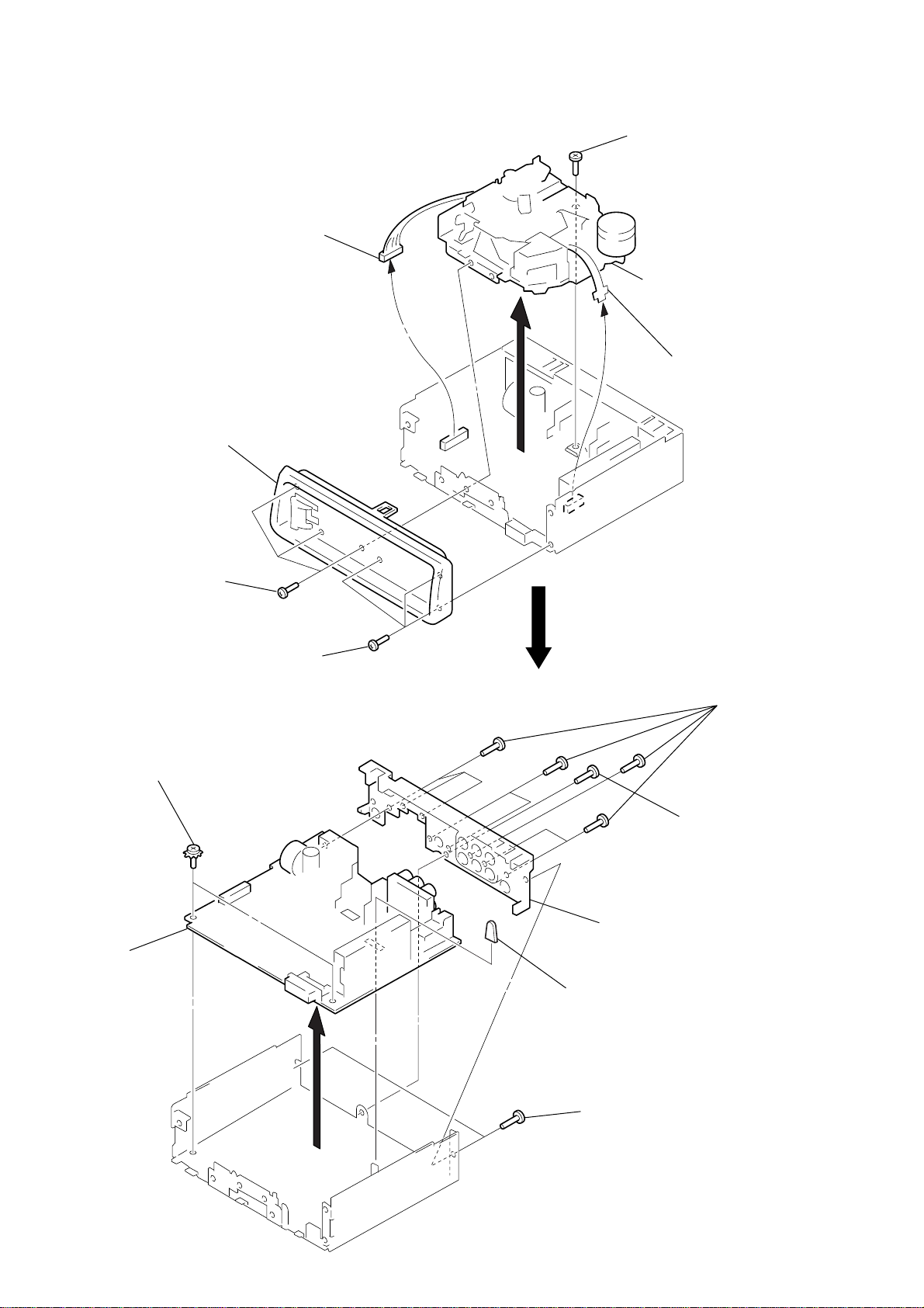
SECTION 2
3
cover ass’y
1
2
2
1
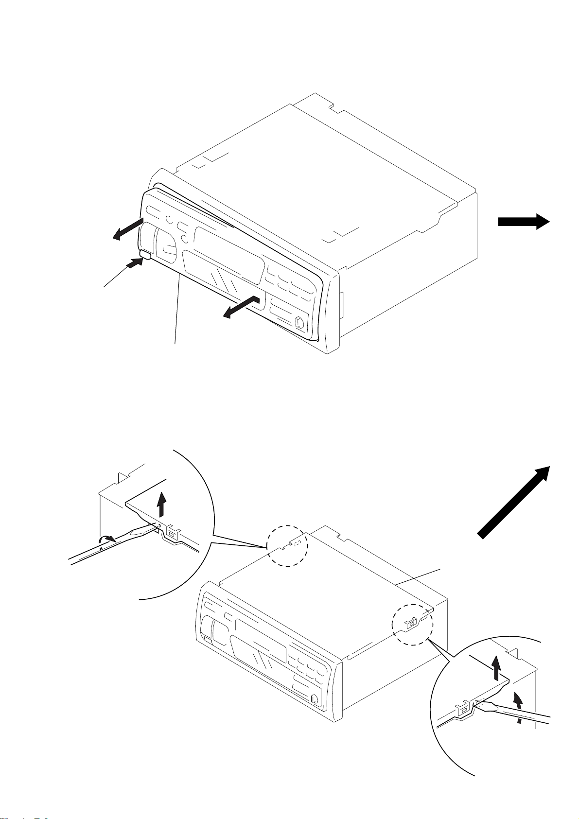
DISASSEMBLY
Note: Follow the disassembly procedure in the numerical order given.
FRONT PANEL ASS’Y
1
Push the button
(release)
COVER ASS’Y
2
Remove the front panel ass’y
to the direction of the arrow
A
A
.
– 9 –
Page 10
)
SUB PANEL, MECHANISM DECK (MG-25F-136)
3
connector
(CNP331)
2
sub panel
5
screw
(PTT2.6
6
mechanism deck
(MG-25F-136)
4
×
6)
flexible flat cable
(CNP301)
1
three screws
(PTT2.6
×
6)
1
MAIN BOARD, HEAT SINK
3
two ground point
screws
4
main board
three screws
(PTT2.6
×
6)
6
heat sink
2
rubber cap (25)
1
screw
(PTT2.6
5
eight screws
(PTT2.6
×
6)
×
10
– 10 –
1
two screws
(PTT2.6
×
6)
Page 11
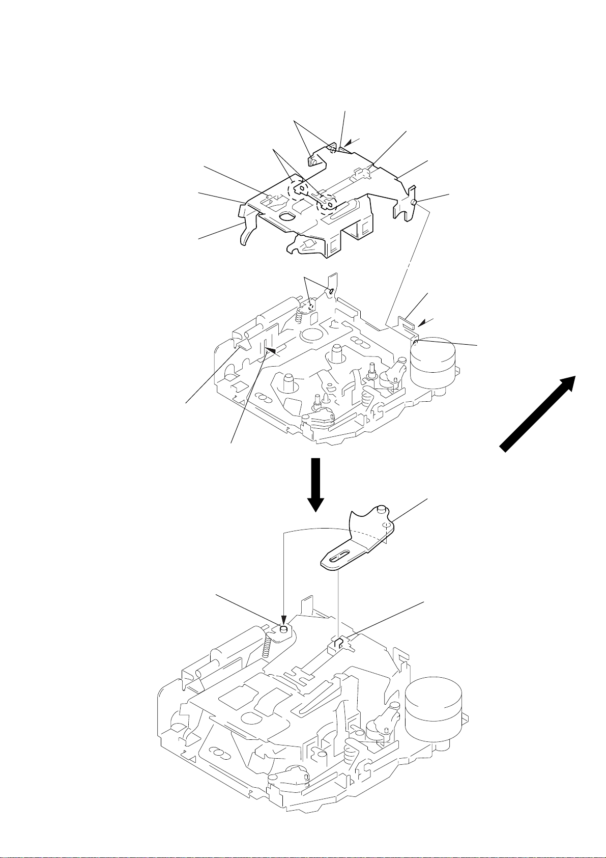
SECTION 3
2
Move the arm (suction) in the arrow
direction and fit on projection.
1
Fit the arm (suction) on the shaft.
projection
ASSEMBLY OF MECHANISM DECK
Note: Follow the assembly procedure in the numerical order given.
HOUSING
4
Fit claw on B part.
3
Put the housing
under A part.
housing
5
Fit projection on C part.
2
Install the hanger onto
two claws of the housing.
C
part
7
Holder the hanger by bending the claw.
1
Install the catch to the hanger.
hanger
6
Fit projection on D part.
8
Hold the hanger by
bending the claw.
D
part
ARM (SUCTION)
A
part
B
part
– 11 –
Page 12
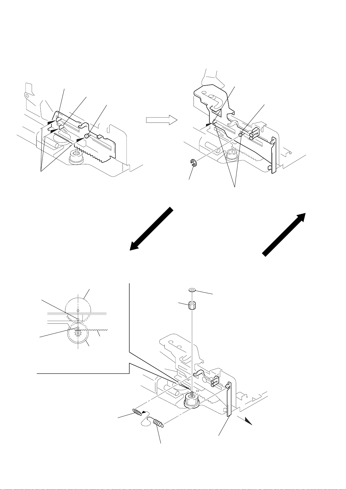
LEVER (LDG-A) / (LDG-B)
shaft
A
shaft
1
Fit the lever (LDG-A) on
shafts A – C and install it.
B
shaft
C
3
type-E stop ring 2.0
shaft
A
Fit the lever (LDG-B) on
2
shafts
install it.
A
and B and
shaft
B
GEAR (LDG-FT)
hole
hole
4
gear (LDG-D)
lever (LDG-A)
gear (LDG-FB)
Align hole in the gear (LDG-D)
with hole the lever (LDG-A)
2
tension spring (LD-2)
5
gear (LDG-FT)
1
6
polyethylene washer
2
tension spring (LD-1)
– 12 –
3
Move the lever (LDG-B)
in the arrow direction.
Page 13

GUIDE (C)
2
guide (C)
1
three claws
– 13 –
Page 14

SECTION 4
MECHANICAL ADJUSTMENTS
SECTION 5
ELECTRICAL ADJUSTMENTS
1. Clean the following parts with a denatured-alcohol-moistened
swab:
playback head pinch roller
rubber belt capstan
idler
2. Demagnetize the playback head with a head demagnetizer.
3. Do not use a magnetized screwdriver for the adjustments.
4. After the adjustments, apply suitable locking compound to the
parts adjusted.
5. The adjustments should be performed with the power supply
voltage unless otherwise noted.
• Torque Measurement
Mode Torque Meter Meter Reading
Forward CQ-102C
Forward
Back Tension (0.01 - 0.06 oz•inch)
Reverse CQ-102RC
Reverse
Back Tension (0.01 - 0.06 oz•inch)
FF, REW CQ-201B
CQ-102C
CQ-102RC
30 - 65 g•cm
(0.42 - 0.90 oz•inch)
0.5 - 4.5g•cm
30 - 65 g•cm
(0.42 - 0.90 oz•inch)
0.5 - 4.5g•cm
60 - 200 g•cm
(0.83 - 2.78 oz•inch)
• T ape Tension Measurement
Mode Tension Meter Meter Reading
Forward CQ-403A
Reverse CQ-403R
more than 90 g
(more than 3.18 oz)
more than 90 g
(more than 3.18 oz)
TEST MODE
This set have the test mode function. In the test mode, FM Auto
Scan/Stop Level and AM (MW) Auto Scan/Stop Lev el adjustments
can be performed easier than it in ordinary procedure.
<Set the Test Mode>
1. Set the “power select” switch (S701) is “A (ON) ” position.
2. Turn ON the regulated power supply. (All LEDs on the set
lights up, and the clock is displayed.)
Note: Press the [OFF] button, if the clock is not displayed.
3. Push the preset [4] button.
4. Push the preset [5] button.
5. Press the preset [1] button for more than two seconds.
6. Then the display indicates all lights, the test mode is set.
<Release the Test mode>
1. Push the [OFF] button.
2. Return the “power select” switch (S701) to initially set position.
See the adjustment location from on page 18 for the
adjusutment.
TAPE DECK SECTION 0 dB=0.775 V
Tape Speed Adjustment
Setting:
speed checker
or
test tape
WS-48A
(3 kHz, 0 dB)
frequency counter
10 k
Ω
set
LINE OUT
+–
Procedure:
1. Put the set into the FWD PB mode.
2. Adjust adjustment resistor for inside capstan motor so that the
reading on the speed checker or frequency counter becomes in
specification.
Specification: Constant speed
Speed checker Frequency counter
–1.5 to +2.5% 2,955 to 3,075Hz
Adjustment Location: See page 18.
– 14 –
Page 15

DOLBY Level Adjustment
r
Setting:
Preset [3] (DOLBY) button : NR OFF
SEL (BAS) button : Center
SEL (TRE) button : Center
SEL (BAL) button : Center
SEL (FAD) button : Center
SEL (VOL) button : Maximum
D-BASS control : OFF
test tape
P-4-D400
(400 Hz, 0 dB)
MAIN board
TP (DOLBY L)/
TP (DOLBY R)
set
level mete
MAIN board
TP (GND)
+
–
Procedure:
1. Put the set into the FWD PB mode.
2. Adjust RV121 (L-CH) and RV221 (R-CH) so that the level
meter reading is –6 ± 1 dB (0.35 to 0.43 V).
Adjustment Location: See page 18.
TUNER SECTION 0 dB=1 µV
Cautions during repair
When the tuner unit is defective, replace it by a new one because
its internal block is difficult to repair.
Note: Adjust the tuner section in the sequence shown below.
1. FM Auto Scan/Stop Level Adjustment
2. FM Stereo Separation Adjustment
3. AM (MW) Auto Scan/Stop Level Adjustment
4. FM POLAR Adjustment
FM Auto Scan/Stop Level Adjustment
Setting:
[SOURCE] button: FM
FM RF signal
generator
Carrier frequency : 98.0 MHz
Output level : 22 dB (12.6
Mode : mono
Modulation : 1 kHz, 22.5 kHz deviation (30%)
Procedure:
1. Set to the test mode. (See page 14).
2. Push the [SOURCE] button and set to FM.
antenna jack (J1)
0.01 µF
set
µ
V)
Display
FM
SHUF1
3. Push the preset
[3] button.
Display
FM
SHUF1
4. Adjust with the volume R V2 on TU1 so that the “FM” indication turns to “FM0” indication on the display window.
But, in case of already indicated “FM0”, turn the RV2 so that
put out light “0” indication and adjustment.
Display
SHUF1
Adjustment Location: See page 18.
– 15 –
Page 16

FM Stereo Separation Adjustment
µ
Setting:
[SOURCE] button: FM
FM RF signal
generator
Carrier frequency : 98.0 MHz
Output level : 70 dB (3.2 mV)
Mode : stereo
Modulation : main: 1 kHz, 20 kHz deviation (26.7%)
antenna jack (J1)
0.01 µF
set
sub: 1 kHz, 20 kHz deviation (26.7%)
19 kHz pilot: 7.5 kHz deviation (10%)
10 k
LINE OUT
level meter
Ω
AM (MW) Auto Scan/Stop Level Adjustment
Make this adjustment after “FM Auto Scan/Stop Le vel Adjustment”.
Setting:
[SOURCE] and [MODE] button: MW
30
Ω
15 pF
+
–
AM RF signal
generator
AM dummy antenna
(50 Ω)
65 pF
set
Procedure:
FM Stereo
signal generator
output channel
L-CH L-CH A
R-CH L-CH Adjust RV4 on TU1
R-CH R-CH C
L-CH R-CH Adjust RV4 on TU1
L-CH Stereo separation: A-B
R-CH Stereo separation: C-D
The separations of both channels should be equal.
Specification: Separation more than 28 dB
Adjustment Location: See page 18.
Level meter Level meter
connection reading (dB)
for minimum reading.
for minimum reading.
B
D
Carrier frequency : 999 kHz
30% amplitude
modulation by
1 kHz signal
Output level : 33 dB (44.7
Procedure:
1. Set to the test mode. (See page 14.)
2. Push the [SOURCE] button and set to FM.
3. Push the [MODE] button and set to MW.
Display
antenna jack (J1)
V)
MW
999
4. Push the preset [3] button.
Display
SHUF1
MW
3
5. Adjust with the volume RV1 on TU1 so that the “MW” indication turns to “MW0” indication on the display window.
But, in case of already indicated “MW0”, turn the R V1 so that
put out light “0” indication and adjustment.
999
SHUF1
Display
3
Adjustment Location: See page 18.
999
SHUF1
– 16 –
Page 17

FM Polar VCO Adjustment
Setting:
[SOURCE] button: FM
FM RF signal
generator
Carrier frequency : 69.5 MHz
Output level : 66 dB (1.995 mV)
MAIN board
TP (VCO)
antenna jack (J1)
set
frequency counter
+
–
Procedure:
1. Tune the set to 69.5 MHz, and set the internal modulation level
of the FM RF signal generator to 10 kHz deviation (20%).
2. Connect the frequency counter to the TP (VCO) on MAIN
board.
3. Adjust RV402 so that the reading on the frequency counter
becomes to 31.25 ± 0.1 kHz.
Adjustment Location: See page 18.
FM Polar Pilot Adjustment
Setting:
[SOURCE] button: FM
FM RF signal
generator
Carrier frequency : 69.5 MHz
Output level : 66 dB (1.995 mV)
MAIN board
TP (PLT)
antenna jack (J1)
set
level meter
+
–
Procedure:
1. Connect the level meter to the TP (PLT) on MAIN boar d.
2. Set the modulation frequency of the FM RF signal generator
to 1 kHz, 40 kHz deviation (80 %)
3. Then output level is supposing that (A) dB.
4. Set the modulation frequency of the FM RF signal generator
to 31.25 kHz, 10 kHz deviation (20%)
5. Adjust L401 so that the reading on the level meter becomes to
maximum.
6. Adjust RV401 so that the reading on the level meter becomes
to (A) + 13.0 dB ± 0.5 dB.
Adjustment Location: See page 18.
– 17 –
Page 18

Adjustment Location:
Tape Speed Adjustment
– SET UPPER VIEW –
RV402 VCO Frequency Adjustment
RV401
L401
TU1
RV1 AM (MW) Auto Scan/Stop Level Adjustment
RV2 FM Auto Scan/Stop Level Adjustment
RV4 FM Stereo Separation Adjustment
Sub Carrier Adjustment
RV221
(R-CH)
– MAIN BOARD (CONDUCTOR SIDE) –
J1
antenna jack
TP
(PLT)
TU1
RV121
(L-CH)
DOLBY Level
Adjustment
IC401
TP
(VCO)
TP (DOLBY R)
TP (GND)
TP (DOLBY L)
A
(ON)
↑
B
(OFF)
S701
power select
switch
– 18 –
Page 19

SECTION 6
DIAGRAMS
• MAIN BOARD IC701 µPD78058GC-F36-3B9 (SYSTEM CONTROLLER)
Pin No. Pin Name I/O Function
1 DSEL I Destination setting terminal (fixed at center voltage)
2 RCIN0 I Rotary remote commander shift key A/D input terminal
3 SD IN I
4 AVSS — Ground terminal (for A/D converter)
5 ST I/O
6 PLLCE O PLL serial chip enable output to the FM/AM PLL (IC31)
7 AVREF1 I Reference voltage (+5V) input terminal (for D/A converter)
8 PLLSI I PLL serial data input from the FM/AM PLL (IC31)
9 PLLSO O PLL serial data output to the FM/AM PLL (IC31)
10 PLLCKO O PLL serial data transfer clock signal output to the FM/AM PLL (IC31)
11 P-STIN I Polar stereo signal input from the polar multiplexer (IC401)
12 LCDSO O Serial data output to the liquid crystal display driver (IC901)
13 LCDCKO O Serial data transfer clock signal output to the liquid crystal display driver (IC901)
14 LCDCE O Chip enable output to the liquid crystal display driver (IC901)
15 LCDINH O
16 UNISI I Serial data input from the bus interface (IC571) (for SONY bus)
17 UNISO O Serial data output to the bus interface (IC571) (for SONY bus)
18 UNICKI I Serial data reading clock signal input terminal (for SONY bus)
19 UNICKO O Serial data transfer clock signal output to the bus interface (IC571) (for SONY bus)
20 BUSON O Bus on/off control signal output to the bus interface (IC571) (for SONY bus) “L”: bus on
21 SYSRST O Reset signal output to the bus interface (IC571) (for SONY bus) “L”: reset
22 AMPON O Standby control signal output to the power amplifier (IC471) “L”: standby
23 AMPMUTE O Muting control signal output to the power amplifier (IC471) “L”: muting on
24 TUNON O Tuner system power supply on/off control signal output to the BA3918 (IC601) “H”: tuner on
25 FM ON O FM system power supply on/off control signal output to the BA3918 (IC601) “H”: FM on
26 PW ON O Main system power supply on/off control signal output to the BA3918 (IC601) “H”: power on
27 COLOR I
Station detector detect input from the FM/AM tuner unit (TU1)
Stop level for SEEK, BTM, etc. is determined SD is present at input of “H”
Input of FM stereo detection signal from FM/AM tuner unit (TU1), and output of forced
monaural control signal to FM/AM tuner unit (TU1) (Commonly used for stereo display input
and forced monaural output)
FM stereo detection at input of “L”, forced monaural at output of “L”
Blank indicate control signal output to the liquid crystal display driver (IC901)
“L”: no display
Input terminal to set whether the illumination color change function is present or not
“L”: illumination color change function is present (fixed at “L”)
28 AMS ON O
29 REL I Reel table rotation detect signal input from the take-up and supply reel sensor
30 MTLIN I
31 POS3 I
32 POS2 I
33 GND — Ground terminal
34 POS0 I
35 POS1 I
36 LM LOD O
37 LM EJ O
Tape auto music sensor control signal output to the CXA2510Q (IC321)
“L” is output to lower the gain for audio level at FF/REW
Input terminal to set whether the auto metal function is present or not
“L”: auto metal function is present Not used this function in this set (fixed at “H”)
Tape position detect input from the tape operation switch on the mechanism block
Tape position detect input from the tape operation switch on the mechanism block
Loading/tape operation motor control signal output to the LB1638M (IC651)
(For the loading direction and forward side operation) *1
Loading/tape operation motor control signal output to the LB1638M (IC651)
(For the eject direction and reverse side operation) *1
– 19 –
Page 20

Pin No. Pin Name I/O Function
38 N/R OUT O
39 NC I Not used (fixed at “H”)
40 CMON O Capstan/reel motor (M901) drive signal output terminal “H”: motor on
41 TAPEON O Tape system power supply on/off control signal output terminal “H”: tape on
42 COLSEL I Setting terminal for the illumination color “L”: amber, “H”: green (fixed at “H”)
43 RCIN1 I Rotary remote commander shift key A/D input terminal
44 TEST I Setting terminal for the test mode “L”: test mode (normally fixed at “H”)
45 ILLON O
46 BEEP O Beep sound output terminal
47 MUTE O Line muting control signal output terminal “H”: line muting on
48 VOLCE O Chip enable signal output to the electrical volume (IC351)
49 SUBCE O Chip enable signal output terminal Not used in this set (open)
50 VOLCKO O Serial data transfer clock signal output to the electrical volume (IC351)
51 SUBCKO O Serial data transfer clock signal output terminal Not used in this set (open)
52 VOLSO O Serial data output to the electrical volume (IC351)
53 TAPMUT O Tape muting on/off control signal output to the CXA2510Q (IC321) “H”: tape muting on
Forward/reverse direction control signal output to the CXA2510Q (IC321)
“L: forward direction, “H”: reverse direction
Power supply on/off control signal output terminal at the illumination and liquid crystal display
driver (IC901) “H”: power on
At power select switch (S701) on mode: “H” output at the accessory on
At power select switch (S701) off mode: “H” output at the power on
Dolby control in/out terminal
54 DOLON I/O
55 DOLBC I/O
56 AMSIN I
57 MTLSEL I/O
58 AD ON O Power supply on/off control signal output for the A/D converter “L”: power on
59 RAMBU I
60 RESET I
61 SIRCS I Sircs signal input terminal Not used in this set (fixed at “H”)
62 BUIN I Battery detect signal input terminal “H”: battery on
63 PW SEL I Power select switch (S701) input terminal “L”: off (halt mode), “H”: on (operation mode)
64 ACCIN I Accessory detect signal input terminal “L”: accessory on
65 NOSESW I Detects the removal of the attaching and removing type front panel block “L”: attaching
66 TELMUTE I Telephone muting signal input terminal At input of “L”, the signal is attenuated by –20 dB
67 KEYACK I
At initial mode: valid/invalid selection input of dolby function (“L” input: valid)
At normal mode: dolby on/off control signal output to the CXA2510Q (IC321)
“H”: dolby on
Dolby B/C selection control in/out terminal
At initial mode: dolby B only/dolby B and C type selection input (“L” input: dolby B and C)
At normal mode: dolby type selection signal output “L”: dolby B, “H”: dolby C
Not used this function (fixed at “H”)
Whether a music is present or not from CXA2510Q (IC321) is detected at auto music sensor
“L”: music is present, “H”: music is not present
METAL control in/out terminal
At initial mode: auto/manual mode selection input of METAL function “L”: manual mode
At manual mode: METAL on/off control signal output to the CXA2510Q (IC321)
“H”: METAL on
At auto mode: input at MTLIN (pin #º)
Internal RAM reset detection signal input from the RN5VD23AA (IC552)
Input terminal to check that RAM data are not destroyed due to low voltage
This checking is made within 100 msec after reset
System reset signal input from the reset signal generator (IC551)
“L” is input for several 100 msec after power on, then it changes to “H”
Input of acknowledge signal for the key entry Acknowledge signal is input to accept function
and eject keys in the power off status On at input of “L”
– 20 –
Page 21

Pin No. Pin Name I/O Function
68 VDD — Power supply terminal (+5V)
69 X OUT O Main system clock output terminal (5 MHz)
70 X IN I Main system clock input terminal (5 MHz)
71 GND — Ground terminal
72 XT OUT O Sub system clock output terminal (32.768 kHz)
73 XT IN I Sub system clock input terminal (32.768 kHz)
74 AVDD — Power supply terminal (+5V) (for A/D converter)
75 AVREF0 I Reference voltage input terminal (+5V) (for A/D converter)
Key input terminal (A/D input)
76 KEYIN0 I
77 KEYIN1 I
78 D.BASS I D-BASS switch (SW951) input (A/D input)
79 VSM I FM and AM signal meter voltage detection input from the FM/AM tuner unit (TU1)
80 KEYSEL I Setting terminal for the key (fixed at center voltage)
*1 loading/tape operation motor control
MODE
TERMINAL
LM LOD (pin #§) “L” “H” “L” “H”
LM EJ (pin #¶) “L” “L” “H” “H”
OFF, SOURCE, MODE *, + ) + SEEK AMS, – = 0 SEEK AMS, VOLUME –,
SEL, VOLUME +, DSPL, ATT keys input (LSW901 to LSW910)
Key input terminal (A/D input)
6, INTRO 1, REPEAT 2, SHUF/a 3, BL SKIP 6, ATA 5, BANK/MTL 4, BTM SENS,
FILE, PRESET DISC +/– keys input (LSW921 to LSW931)
STOP
LOADING/
FORWARD
EJECT/
REVERSE
BRAKE
– 21 –
Page 22

1 IC31 1 (X OUT)
139 nsec
2 IC701 &™ (XT OUT)
30.6 µsec
3.6 Vp-p
5.7 Vp-p
3 IC701 ^ª (X OUT)
200 nsec
5.5 Vp-p
– 22 –
Page 23

• Semiconductor Location
(Component Side)
Ref. No. Location
D1 F14
D176 C-7
D177 B-6
D186 C-7
D187 C-7
D276 C-6
D277 C-5
D286 C-7
D287 C-6
D421 I-8
D422 I-9
D423 J-12
D424 J-9
D425 G-8
D426 J-9
D480 C-5
D481 D-5
D551 K-10
D552 I-4
D606 D-4
IC31 J-11
IC321 H-11
IC351 F-9
IC431 F-11
IC441 F-12
IC551 I-3
IC552 I-4
IC571 D-1
IC651 H-2
IC701 I-7
6-2. PRINTED WIRING BOARD – MAIN Section –
Q1 I-14
Q32 J-9
Q51 J-13
Q52 J-12
Q171 A-12
Q181 A-12
Q271 A-12
Q281 A-12
Q331 I-3
Q332 H-3
Q333 H-3
Q334 G-4
Q335 H-4
Q371 F-4
Q372 F-6
Q401 G-14
Q420 I-9
Q421 I-8
Q551 K-9
Q552 K-10
Q601 E-4
Q623 J-4
Q624 J-3
Note on Printed Wiring Board:
• X : parts extracted from the component side.
¢
•
• b : Pattern from the side which enables seeing.
(The other layers' patterns are not indicated.)
: internal component.
Caution:
Pattern face side: Parts on the pattern face side seen from
(Conductor Side) the pattern face are indicated.
Parts face side: Parts on the parts face side seen from
(Component Side) the parts face are indicated.
– 23 – – 24 –
Page 24

• Semiconductor Location
(Conductor Side)
Ref. No. Location
D31 I-6
D51 K-2
D331 H-12
D332 G-13
D371 F-9
D372 E-9
D373 F-8
D374 F-8
D471 C-11
D472 F-10
D473 D-10
D571 C-14
D572 C-14
D573 B-14
D574 B-14
D601 D-11
D602 D-11
D603 C-14
D604 E-10
D605 K-5
D621 K-13
D665 K-2
D666 J-3
D671 J-3
D672 J-4
D673 J-3
D674 J-4
D675 J-4
D676 J-4
IC401 E-4
IC471 B-7
IC601 E-14
Q422 K-6
Q423 J-5
Q424 K-6
Q602 D-13
Q625 J-12
Q626 J-13
– 25 – – 26 –
Page 25

• IC Block Diagrams – MAIN Board –
IC31 BU2624F-E2
1
XOUT
XIN
2
REFERENCE
DIVIDER
PHASE
DETECT
20
VSS
19
PD1
18
VDD
3
CE
4
CK
5
DA
6
CD
7
P0
8
P1
9
P3
10
P4
I/O
CONTROL
20BIT COUNT
IC321 CXA2510AQ-T4
SHIFT
REGISTER
LATCH
MAIN
COUNT
IF COUNT
CONTROL
PRESCALLER
17
FMIN
16
AMIN
15
P2
14
IF1
13
IF2
12
SD
11
PD2
PBFB1
PBRIN1
PBREF1
PBFIN1
VCT
PBGND
PBFIN2
PBREF2
PBRIN2
PBFB2
MSSW
NC
TCH1
LINEOUT1
MSLPF
NR BIAS
TAPE/AUX
TAPE EQ
FWD/RVS
VCC
+
–
F3
–
+
LINEOUT2
DIREF
+
OFF/B
NR
2425
TCH2
2122232627282930
NR
–
OFF/B
MS
MODE
NR
MODE
DETECT
NC
PLAY
MS ON/
OFF
20
19
18
17
16
15
14
13
12
11
MSMODE
DRSW
TAPESW
INSW
NRSW
NC
MSOUT
DGND
MSTC
FF
AUXIN1
PBEQ1
–
31
32
33
34
35
36
37
38
39
40
F2
VCT
F1
–
1
PBEQ2
TAPEIN1
PBOUT1
GND
120µ/
70µ
+
+
120µ/
70µ
345 6 7 8 9 10
2
VCC
PBOUT2
X1
+
X1
TAPEIN2
T2
LPF
T1
AUXIN2
– 35 –
Page 26

IC351 LC75373ED
+
–
+
–
CONTROL
CIRCUIT
1
2
3
4
5
6
7
8
SWC
IN+A
IN–A
–VCC
OUT
IN–B
IN+B
+VCC
LSELO
VDD
RSELO
SHIFT
REGISTER
2324252627282930313233
11
LSOUT
CONTROL
RSOUT
22
LFIN
+
–
+
–
–
+
–
+
LFOUT
21
LROUT
20
19
VREF
18
CE
17
DI
16
CL
15
VSS
14
RROUT
RFOUT
13
12
RFIN
LS3
LS1
LSIN
LT3
LT2
LVRIN
34
35
L4
L3
36
L2
37
L1
38
39
R1
40
41
R2
R3
42
R4
43
44
1
RVRIN
LCOM
+
–
+
–
–
+
–
+
2 345 6 7 8 9 10
RCOM
LT1
+
–
+
–
+
–
–
+
RT1
RT2
RT3
LTOUT
–
+
DECODER LATCH
+
–
RS1
RSIN
RTOUT
LS2
–
+
–
+
+
–
+
–
RS2
RS3
IC401 IR3R42
SUBIN
SUBOUT
AMP
1
VCC
MON
1/2
PHASE
AMP
2 3
IN
WAVEFORM
SEP.
GATE
POUT
20 19 18 17 16 15 14 13 12 11
REGULATOR
VCO
OSC
1/2
SAMPLE
& HOLD
BUFFER
4
RHC
LPF1A
LPF1B
DETIN
LPF2A
AMP
PHASE
COMPARATOR
PHASE
COMPARATOR 2
MUTE
5 6 7 8 9 10
ROUT
LOUT
ST
VCO STOP
LHC
IC471 TDA7384
DRIVER
DRIVER
DRIVER
LPF2B
TRIGGER
DRIVER
GND
LAMP
IC431, 441 M5201FP
GND
OUT1–
10 12
9
OUT1+
SVR
11
14
16
S-GND
IN4
17
15
IN3
OUT3+
AC-GND
1918
GND
OUT3–
IN1
13
IN2
20
VCC
21
OUT4+
2322
MUTE
24
OUT4–
25
GND
N.C.
– 36 –
5
3 4
1
2
TAB
GND
OUT2–
OUT2+
STNBY
7 8
6
VCC
Page 27

IC552 RN5VD23AA-TL
IC571 BA8270F-E2
1
OUT
IC601 BA3918-V3
–
+
CD
5
2 3
VDD
REGULATOR
OVER VOLTAGE
4
VREF
+
–
PROTECT
NC
GND
–
+
–
+
BUS ON
1
2
RST
BATT
3
4
CLK
5
VREF
6
DATA
GND
7 8
–
+
BUS ON
SWITCH
RESET
SWITCH
BATTERY
SWITCH
14
13
12
11
10
9
VCC
RST
BUS ON
CLK IN
BU IN
DATA IN
DATA OUT
2 3
4
1
NC
STB
MODE2
MODE1
5 6 7 8 9 10 1211
VDD
IC651 LB1638M
1
GND
2
IN1
VCC
3
4
IN2
5 6
GND
CONTROL LOGIC
AMP
VCC
ANT
10
COM
N.C.
9
OUT1
VS
8
7
OUT2
N.C.
AM
FM
GND
– 37 –
Page 28

SECTION 7
EXPLODED VIEWS
NOTE:
• -XX and -X mean standardized parts, so they
may have some difference from the original
one.
• Color Indication of Appearance Parts
Example:
KNOB, BALANCE (WHITE) . . . (RED)
↑↑
Parts Color Cabinet's Color
(1) CHASSIS SECTION
MG-25F-136
• Items marked “*” are not stocked since they
are seldom required for routine service. Some
delay should be anticipated when ordering
these items.
• The mechanical parts with no reference number in the exploded views are not supplied.
• Hardware (# mark) list and accessories and
packing materials are given in the last of the
electrical parts list.
7
13
#1
14
F401
15
Front panel ass’y
#2
6
8
#1
#4
#4
#1
#4
5
9
10
4
2
3
11
12
#1
#1
1
Ref. No. Part No. Description Remark
1 3-009-294-01 PANEL, SUB
2 3-913-076-01 SPRING (C DOOR), TORSION
3 3-922-165-21 DOOR, CASSETTE
4 X-3367-636-1 LOCK ASSY
* 5 A-3313-526-A MAIN (B) BOARD, COMPLETE
6 3-915-923-01 SCREW, GROUND POINT
7 X-3373-751-1 COVER ASSY
* 8 3-018-390-01 BRACKET (IC)
Ref. No. Part No. Description Remark
* 9 3-018-389-11 HEAT SINK
10 3-338-263-01 CUSHION (U)
* 11 3-010-378-01 INSULATOR
* 12 3-009-810-01 CHASSIS
13 3-012-859-01 CAP (25), RUBBER
* 14 3-355-209-01 PLATE (B), GROUND
15 1-776-207-81 CORD (WITH CONNECTOR) (POWER)
F401 1-532-877-11 FUSE (BLADE TYPE) (AUTO FUSE) (10A)
– 38 –
Page 29

5
(2) FRONT PANEL SECTION
54
55
56
53
57
58
not supplied
(KEY board)
70
65
66
67
68
69
LCD901
64
59
63
60
#5
#
61
62
51
52
Ref. No. Part No. Description Remark
51 X-3374-685-1 PANEL SUB ASSY
52 3-018-799-01 BUTTON (D-BASS)
53 3-016-932-01 BUTTON (L) (2) (+, -)
54 3-009-304-01 BUTTON (RELEASE)
55 3-918-693-01 SPRING (RELEASE)
56 3-904-194-01 EMBLEM (NO. 2.5), SONY
57 3-009-300-01 BUTTON (SOURCE)
58 3-018-658-01 BUTTON (L) (+ +), SEEK AMS,
=0 -, r, OFF , r, SEL, ATT)
59 3-009-295-01 PANEL, FRONT BACK
* 60 3-015-038-01 CUSHION (BACK PANEL)
* 61 3-018-611-01 HOLDER (LCD)
Ref. No. Part No. Description Remark
* 62 3-018-612-01 PLATE, LIGHT GUIDE
* 63 3-019-149-01 PLATE, LCD
* 64 3-019-150-01 SHEET (REFLECTOR)
* 65 3-019-151-01 PLATE (LCD), GROUND
66 3-016-933-01 BUTTON (1-3) (6, 1, 2, 3)
67 3-016-931-11 BUTTON (4-6) (4, 5, 6)
68 3-016-937-01 BUTTON (R) (S) (SENS, FILE, - DISK +)
* 69 3-024-391-01 SHEET (LCD)
* 70 3-024-846-01 SHEET (LCD) (B)
LCD901 1-801-968-21 DISPLAY PANEL, LIQUID CRYSTAL
– 39 –
Page 30

(3) MECHANISM DECK SECTION
(MG-25F-136)
154
153
#6
155
158
152
157
156
159
A
160
A
161
163
HP901
162
M901
164
165
168
151
Ref. No. Part No. Description Remark
151 A-3291-667-A CLUTCH (FR) ASSY
* 152 3-019-130-01 LEVER (LDG-A)
* 153 3-019-131-01 LEVER (LDG-B)
154 3-020-539-01 SPRING (LD-1), TENSION
155 3-020-540-01 SPRING (LD-2), TENSION
156 3-020-542-01 GEAR (LOADING FT)
157 3-341-753-11 WASHER, POLYETHYLENE
158 3-020-533-01 HOUSING
* 159 3-020-532-01 ARM (SUCTION)
160 3-020-534-01 HANGER
#7
168
166
167
Ref. No. Part No. Description Remark
161 3-933-346-01 CATCHER
162 3-933-344-01 GUIDE (C)
163 3-014-798-01 SCREW (HEAD), SPECIAL
164 3-364-151-01 WASHER
165 A-3301-267-A CHASSIS ASSY (G)
166 3-017-302-01 BELT (25)
167 3-936-853-01 FLYWHEEL (F)
168 3-701-437-21 WASHER
HP901 1-500-157-21 HEAD, MAGNETIC (PLAYBACK)
M901 A-3291-665-A MOTOR ASSY, MAIN (CAPSTAN/REEL)
– 40 –
Page 31

SECTION 8
ELECTRICAL PARTS LIST
KEY
NOTE:
• Due to standardization, replacements in the
parts list may be different from the parts specified in the diagrams or the components used
on the set.
• -XX and -X mean standardized parts, so they
may have some difference from the original
one.
• RESISTORS
All resistors are in ohms.
METAL: Metal-film resistor.
METAL OXIDE: Metal oxide-film resistor.
F: nonflammable
Ref. No. Part No. Description Remark
KEY BOARD
**********
* 3-018-611-01 HOLDER (LCD)
* 3-018-612-01 PLATE, LIGHT GUIDE
* 3-019-149-01 PLATE, LCD
* 3-019-150-01 SHEET (REFLECTOR)
* 3-019-151-01 PLATE (LCD), GROUND
< CAPACITOR >
C901 1-163-033-00 CERAMIC CHIP 0.022uF 50V
C902 1-163-038-00 CERAMIC CHIP 0.1uF 25V
C903 1-163-038-00 CERAMIC CHIP 0.1uF 25V
C904 1-163-251-11 CERAMIC CHIP 100PF 5% 50V
< CONNECTOR >
• Items marked “*” are not stocked since they
are seldom required for routine service.
Some delay should be anticipated when ordering these items.
• SEMICONDUCTORS
In each case, u: µ, for example:
uA. . : µA. . uPA. . : µPA. .
uPB. . : µPB. . uPC. . : µPC. .
uPD. . : µPD. .
• CAPACITORS
uF: µF
• COILS
uH: µH
When indicating parts by reference
number, please include the board.
Ref. No. Part No. Description Remark
LSW908 1-762-620-11 SWITCH, KEY BOARD (WITH LED)(+)
LSW909 1-762-620-11 SWITCH, KEY BOARD (WITH LED)(DSPL)
LSW910 1-762-620-11 SWITCH, KEY BOARD (WITH LED)(ATT)
LSW921 1-762-620-11 SWITCH, KEY BOARD (WITH LED)(6)
LSW922 1-762-620-11 SWITCH, KEY BOARD (WITH LED)(1/INTRO)
LSW923 1-762-620-11 SWITCH, KEY BOARD (WITH LED)(2/REPEAT)
LSW924 1-762-620-11 SWITCH, KEY BOARD (WITH LED)(3/SHUF/a)
LSW925 1-762-620-11 SWITCH, KEY BOARD (WITH LED)(6/BL.SKIP)
LSW926 1-762-620-11 SWITCH, KEY BOARD (WITH LED)(5/ATA)
LSW927 1-762-620-11 SWITCH, KEY BOARD (WITH LED)
(4/BANK/MTL)
LSW928 1-762-620-11 SWITCH, KEY BOARD (WITH LED)(SENS/BTM)
LSW929 1-762-620-11 SWITCH, KEY BOARD (WITH LED)(FILE)
LSW930 1-762-620-11 SWITCH, KEY BOARD (WITH LED)
(DISC/PRESET +)
CNP901 1-764-423-11 PIN, CONNECTOR 12P
< DIODE >
D901 8-719-976-99 DIODE DTZ5.1B
D902 8-719-105-99 DIODE RD6.2M-B1
D903 8-719-105-99 DIODE RD6.2M-B1
D904 8-719-105-99 DIODE RD6.2M-B1
D905 8-719-105-99 DIODE RD6.2M-B1
< IC >
IC901 8-759-365-90 IC LC75824W
< CHIP CONDUCTOR >
JC901 1-216-295-00 SHORT 0
< LIQUID CRYSTAL DISPLAY >
LCD901 1-801-968-21 DISPLAY PANEL, LIQUID CRYSTAL
< SWITCH >
LSW901 1-762-620-11 SWITCH, KEY BOARD (WITH LED)(OFF)
LSW902 1-762-620-11 SWITCH, KEY BOARD (WITH LED)(SOURCE)
LSW903 1-762-620-11 SWITCH, KEY BOARD (WITH LED)
LSW904 1-762-620-11 SWITCH, KEY BOARD (WITH LED)(+ +))
LSW905 1-762-620-11 SWITCH, KEY BOARD (WITH LED)(=0 -)
LSW906 1-762-620-11 SWITCH, KEY BOARD (WITH LED)(-)
LSW907 1-762-620-11 SWITCH, KEY BOARD (WITH LED)(SEL)
(MODE *)
LSW931 1-762-620-11 SWITCH, KEY BOARD (WITH LED)
(DISC/PRESET -)
< PILOT LAMP >
PL903 1-517-633-21 LAMP, PILOT (LCD BACK LIGHT)
PL904 1-517-633-21 LAMP, PILOT (LCD BACK LIGHT)
< TRANSISTOR >
Q901 8-729-106-60 TRANSISTOR 2SB1115A
Q902 8-729-106-60 TRANSISTOR 2SB1115A
Q903 8-729-900-53 TRANSISTOR DTC114EK
Q904 8-729-900-53 TRANSISTOR DTC114EK
< RESISTOR >
R901 1-216-647-11 METAL CHIP 680 0.5% 1/10W
R902 1-216-647-11 METAL CHIP 680 0.5% 1/10W
R903 1-216-647-11 METAL CHIP 680 0.5% 1/10W
R904 1-208-437-41 RES, CHIP 1.0K
R905 1-216-655-11 METAL CHIP 1.5K 0.5% 1/10W
R906 1-216-655-11 METAL CHIP 1.5K 0.5% 1/10W
R907 1-208-445-41 RES, CHIP 2.2K
R908 1-208-449-41 RES, CHIP 3.3K
R909 1-208-453-41 RES, CHIP 4.7K
R921 1-216-647-11 METAL CHIP 680 0.5% 1/10W
R922 1-216-647-11 METAL CHIP 680 0.5% 1/10W
R923 1-216-647-11 METAL CHIP 680 0.5% 1/10W
R924 1-208-437-41 RES, CHIP 1.0K
– 41 –
Page 32

KEY MAIN
Ref. No. Part No. Description Remark
R925 1-216-655-11 METAL CHIP 1.5K 0.5% 1/10W
R926 1-216-655-11 METAL CHIP 1.5K 0.5% 1/10W
R927 1-208-445-41 RES, CHIP 2.2K
R928 1-208-449-41 RES, CHIP 3.3K
R929 1-208-453-41 RES, CHIP 4.7K
R930 1-216-671-11 METAL CHIP 6.8K 0.5% 1/10W
R931 1-208-462-41 RES, CHIP 10K
R951 1-216-041-00 METAL CHIP 470 5% 1/10W
R952 1-216-109-00 METAL CHIP 330K 5% 1/10W
R953 1-216-049-11 RES, CHIP 1.0K (2012)
R954 1-216-049-11 RES, CHIP 1.0K (2012)
R955 1-216-049-11 RES, CHIP 1.0K (2012)
R956 1-216-049-11 RES, CHIP 1.0K (2012)
R957 1-216-073-00 METAL CHIP 10K 5% 1/10W
R958 1-216-065-00 METAL CHIP 4.7K 5% 1/10W
R959 1-216-073-00 METAL CHIP 10K 5% 1/10W
R960 1-216-065-00 METAL CHIP 4.7K 5% 1/10W
R961 1-216-037-00 METAL CHIP 330 5% 1/10W
R962 1-216-033-00 METAL CHIP 220 5% 1/10W
R963 1-216-029-00 METAL CHIP 150 5% 1/10W
R964 1-216-025-00 RES, CHIP 100 (2012)
R965 1-216-037-00 METAL CHIP 330 5% 1/10W
R966 1-216-033-00 METAL CHIP 220 5% 1/10W
R967 1-216-029-00 METAL CHIP 150 5% 1/10W
R968 1-216-021-00 METAL CHIP 68 5% 1/10W
R969 1-216-037-00 METAL CHIP 330 5% 1/10W
R970 1-216-031-00 METAL CHIP 180 5% 1/10W
R971 1-216-029-00 METAL CHIP 150 5% 1/10W
R972 1-216-021-00 METAL CHIP 68 5% 1/10W
R981 1-216-655-11 METAL CHIP 1.5K 0.5% 1/10W
R982 1-208-449-41 RES, CHIP 3.3K
R983 1-216-671-11 METAL CHIP 6.8K 0.5% 1/10W
R984 1-216-081-00 METAL CHIP 22K 5% 1/10W
< SWITCH >
SW951 1-762-937-11 SWITCH, ROTARY (D-BASS)
************************************************************
Ref. No. Part No. Description Remark
C24 1-163-809-11 CERAMIC CHIP 0.047uF 10% 25V
C25 1-163-809-11 CERAMIC CHIP 0.047uF 10% 25V
C26 1-163-809-11 CERAMIC CHIP 0.047uF 10% 25V
C31 1-126-157-11 ELECT 10uF 20% 16V
C33 1-163-038-00 CERAMIC CHIP 0.1uF 25V
C34 1-126-157-11 ELECT 10uF 20% 16V
C35 1-164-232-11 CERAMIC CHIP 0.01uF 50V
C36 1-163-251-11 CERAMIC CHIP 100PF 5% 50V
C37 1-163-251-11 CERAMIC CHIP 100PF 5% 50V
C38 1-163-251-11 CERAMIC CHIP 100PF 5% 50V
C39 1-163-231-11 CERAMIC CHIP 15PF 5% 50V
C40 1-163-231-11 CERAMIC CHIP 15PF 5% 50V
C51 1-124-589-11 ELECT 47uF 20% 16V
C52 1-109-982-11 CERAMIC CHIP 1uF 10% 10V
C53 1-163-017-00 CERAMIC CHIP 0.0047uF 5% 50V
C54 1-164-489-11 CERAMIC CHIP 0.22uF 10% 16V
C55 1-124-589-11 ELECT 47uF 20% 16V
C121 1-163-125-00 CERAMIC CHIP 220PF 5% 50V
C122 1-163-125-00 CERAMIC CHIP 220PF 5% 50V
C124 1-136-153-00 FILM 0.01uF 5% 50V
C125 1-164-489-11 CERAMIC CHIP 0.22uF 10% 16V
C126 1-164-232-11 CERAMIC CHIP 0.01uF 50V
C127 1-164-004-11 CERAMIC CHIP 0.1uF 10% 25V
C128 1-126-163-11 ELECT 4.7uF 20% 50V
C129 1-163-227-11 CERAMIC CHIP 10PF 0.5PF 50V
C131 1-164-161-11 CERAMIC CHIP 0.0022uF 10% 100V
C150 1-126-160-11 ELECT 1uF 20% 50V
C151 1-126-163-11 ELECT 4.7uF 20% 50V
C152 1-164-232-11 CERAMIC CHIP 0.01uF 50V
C153 1-126-160-11 ELECT 1uF 20% 50V
C154 1-126-160-11 ELECT 1uF 20% 50V
C155 1-164-182-11 CERAMIC CHIP 0.0033uF 10% 50V
C156 1-163-037-11 CERAMIC CHIP 0.022uF 10% 25V
C157 1-126-157-11 ELECT 10uF 20% 16V
C158 1-164-492-11 CERAMIC CHIP 0.15uF 10% 16V
C159 1-164-492-11 CERAMIC CHIP 0.15uF 10% 16V
C160 1-126-157-11 ELECT 10uF 20% 16V
C171 1-126-163-11 ELECT 4.7uF 20% 50V
* A-3313-526-A MAIN BOARD, COMPLETE
*********************
* 3-018-389-11 HEAT SINK
* 3-018-390-01 BRACKET (IC)
7-685-794-09 SCREW +PTT 2.6X10 (S)
< CAPACITOR >
C1 1-163-235-11 CERAMIC CHIP 22PF 5% 50V
C2 1-126-157-11 ELECT 10uF 20% 16V
C3 1-126-157-11 ELECT 10uF 20% 16V
C4 1-126-157-11 ELECT 10uF 20% 16V
C5 1-163-009-11 CERAMIC CHIP 0.001uF 10% 50V
C6 1-163-009-11 CERAMIC CHIP 0.001uF 10% 50V
C7 1-163-809-11 CERAMIC CHIP 0.047uF 10% 25V
C8 1-164-232-11 CERAMIC CHIP 0.01uF 50V
C9 1-163-038-00 CERAMIC CHIP 0.1uF 25V
C21 1-163-024-00 CERAMIC CHIP 0.018uF 10% 50V
C22 1-163-024-00 CERAMIC CHIP 0.018uF 10% 50V
C23 1-163-809-11 CERAMIC CHIP 0.047uF 10% 25V
C172 1-164-489-11 CERAMIC CHIP 0.22uF 10% 16V
C181 1-126-163-11 ELECT 4.7uF 20% 50V
C182 1-164-489-11 CERAMIC CHIP 0.22uF 10% 16V
C221 1-163-125-00 CERAMIC CHIP 220PF 5% 50V
C222 1-163-125-00 CERAMIC CHIP 220PF 5% 50V
C224 1-136-153-00 FILM 0.01uF 5% 50V
C225 1-164-489-11 CERAMIC CHIP 0.22uF 10% 16V
C226 1-164-232-11 CERAMIC CHIP 0.01uF 50V
C227 1-164-004-11 CERAMIC CHIP 0.1uF 10% 25V
C228 1-126-163-11 ELECT 4.7uF 20% 50V
C229 1-163-227-11 CERAMIC CHIP 10PF 0.5PF 50V
C231 1-164-161-11 CERAMIC CHIP 0.0022uF 10% 100V
C250 1-126-160-11 ELECT 1uF 20% 50V
C251 1-126-163-11 ELECT 4.7uF 20% 50V
C252 1-164-232-11 CERAMIC CHIP 0.01uF 50V
C253 1-126-160-11 ELECT 1uF 20% 50V
C254 1-126-160-11 ELECT 1uF 20% 50V
C255 1-164-182-11 CERAMIC CHIP 0.0033uF 10% 50V
C256 1-163-037-11 CERAMIC CHIP 0.022uF 10% 25V
C257 1-126-157-11 ELECT 10uF 20% 16V
– 42 –
Page 33

MAIN
Ref. No. Part No. Description Remark
C258 1-164-492-11 CERAMIC CHIP 0.15uF 10% 16V
C259 1-164-492-11 CERAMIC CHIP 0.15uF 10% 16V
C260 1-126-157-11 ELECT 10uF 20% 16V
C271 1-126-163-11 ELECT 4.7uF 20% 50V
C272 1-164-489-11 CERAMIC CHIP 0.22uF 10% 16V
C281 1-126-163-11 ELECT 4.7uF 20% 50V
C282 1-164-489-11 CERAMIC CHIP 0.22uF 10% 16V
C321 1-124-234-00 ELECT 22uF 20% 16V
C322 1-135-164-21 TANTAL. CHIP 22uF 20% 20V
C323 1-163-009-11 CERAMIC CHIP 0.001uF 10% 50V
C324 1-107-823-11 CERAMIC CHIP 0.47uF 10% 16V
C325 1-164-232-11 CERAMIC CHIP 0.01uF 50V
C326 1-164-232-11 CERAMIC CHIP 0.01uF 50V
C327 1-126-157-11 ELECT 10uF 20% 16V
C328 1-126-157-11 ELECT 10uF 20% 16V
C332 1-163-038-00 CERAMIC CHIP 0.1uF 25V
C333 1-163-038-00 CERAMIC CHIP 0.1uF 25V
C334 1-126-157-11 ELECT 10uF 20% 16V
C335 1-126-934-11 ELECT 220uF 20% 16V
C336 1-126-157-11 ELECT 10uF 20% 16V
C351 1-124-584-00 ELECT 100uF 20% 10V
C352 1-124-234-00 ELECT 22uF 20% 16V
C358 1-163-009-11 CERAMIC CHIP 0.001uF 10% 50V
C371 1-126-163-11 ELECT 4.7uF 20% 50V
C372 1-126-157-11 ELECT 10uF 20% 16V
C373 1-109-982-11 CERAMIC CHIP 1uF 10% 10V
C401 1-163-038-00 CERAMIC CHIP 0.1uF 25V
C402 1-126-157-11 ELECT 10uF 20% 16V
C403 1-126-160-11 ELECT 1uF 20% 50V
C404 1-137-150-11 FILM 0.01uF 5% 100V
C405 1-137-150-11 FILM 0.01uF 5% 100V
C406 1-163-009-11 CERAMIC CHIP 0.001uF 10% 50V
C407 1-163-009-11 CERAMIC CHIP 0.001uF 10% 50V
C408 1-163-263-11 CERAMIC CHIP 330PF 5% 50V
C409 1-163-009-11 CERAMIC CHIP 0.001uF 10% 50V
C410 1-163-809-11 CERAMIC CHIP 0.047uF 10% 25V
C411 1-163-133-00 CERAMIC CHIP 470PF 5% 50V
C412 1-124-465-00 ELECT 0.47uF 20% 50V
C413 1-124-465-00 ELECT 0.47uF 20% 50V
C414 1-126-160-11 ELECT 1uF 20% 50V
C415 1-109-982-11 CERAMIC CHIP 1uF 10% 10V
C416 1-109-982-11 CERAMIC CHIP 1uF 10% 10V
C417 1-163-141-00 CERAMIC CHIP 0.001uF 5% 50V
C418 1-163-141-00 CERAMIC CHIP 0.001uF 5% 50V
C420 1-164-161-11 CERAMIC CHIP 0.0022uF 10% 100V
C421 1-163-011-11 CERAMIC CHIP 0.0015uF 10% 50V
C422 1-164-161-11 CERAMIC CHIP 0.0022uF 10% 100V
C423 1-163-037-11 CERAMIC CHIP 0.022uF 10% 25V
C424 1-163-017-00 CERAMIC CHIP 0.0047uF 5% 50V
C425 1-107-823-11 CERAMIC CHIP 0.47uF 10% 16V
C431 1-164-182-11 CERAMIC CHIP 0.0033uF 10% 50V
C441 1-164-182-11 CERAMIC CHIP 0.0033uF 10% 50V
C445 1-163-009-11 CERAMIC CHIP 0.001uF 10% 50V
C446 1-126-157-11 ELECT 10uF 20% 16V
C447 1-124-589-11 ELECT 47uF 20% 16V
C451 1-163-251-11 CERAMIC CHIP 100PF 5% 50V
C452 1-163-251-11 CERAMIC CHIP 100PF 5% 50V
C453 1-163-251-11 CERAMIC CHIP 100PF 5% 50V
Ref. No. Part No. Description Remark
C454 1-163-251-11 CERAMIC CHIP 100PF 5% 50V
C455 1-163-251-11 CERAMIC CHIP 100PF 5% 50V
C456 1-163-251-11 CERAMIC CHIP 100PF 5% 50V
C470 1-164-506-11 CERAMIC CHIP 4.7uF 16V
C471 1-126-937-21 ELECT 4700uF 20% 16V
C472 1-124-589-11 ELECT 47uF 20% 16V
C473 1-107-682-11 CERAMIC CHIP 1uF 10% 16V
C474 1-165-319-11 CERAMIC CHIP 0.1uF 50V
C475 1-165-319-11 CERAMIC CHIP 0.1uF 50V
C476 1-165-319-11 CERAMIC CHIP 0.1uF 50V
C477 1-163-243-11 CERAMIC CHIP 47PF 5% 50V
C478 1-126-160-11 ELECT 1uF 20% 50V
C479 1-126-096-11 ELECT 10uF 20% 35V
C480 1-124-589-11 ELECT 47uF 20% 16V
C481 1-164-232-11 CERAMIC CHIP 0.01uF 50V
C482 1-163-038-00 CERAMIC CHIP 0.1uF 25V
C483 1-109-982-11 CERAMIC CHIP 1uF 10% 10V
C551 1-164-004-11 CERAMIC CHIP 0.1uF 10% 25V
C552 1-125-701-11 CAPACITOR 0.047F 0 5.5V
C553 1-126-925-11 ELECT 470uF 20% 10V
C554 1-164-004-11 CERAMIC CHIP 0.1uF 10% 25V
C555 1-164-004-11 CERAMIC CHIP 0.1uF 10% 25V
C556 1-164-004-11 CERAMIC CHIP 0.1uF 10% 25V
C571 1-163-038-00 CERAMIC CHIP 0.1uF 25V
C572 1-163-038-00 CERAMIC CHIP 0.1uF 25V
C601 1-126-163-11 ELECT 4.7uF 20% 50V
C602 1-164-232-11 CERAMIC CHIP 0.01uF 50V
C603 1-164-232-11 CERAMIC CHIP 0.01uF 50V
C604 1-126-157-11 ELECT 10uF 20% 16V
C605 1-124-589-11 ELECT 47uF 20% 16V
C606 1-126-157-11 ELECT 10uF 20% 16V
C607 1-126-157-11 ELECT 10uF 20% 16V
C608 1-126-157-11 ELECT 10uF 20% 16V
C609 1-126-157-11 ELECT 10uF 20% 16V
C610 1-163-038-00 CERAMIC CHIP 0.1uF 25V
C621 1-126-157-11 ELECT 10uF 20% 16V
C622 1-163-038-00 CERAMIC CHIP 0.1uF 25V
C665 1-164-004-11 CERAMIC CHIP 0.1uF 10% 25V
C666 1-164-004-11 CERAMIC CHIP 0.1uF 10% 25V
C667 1-163-038-00 CERAMIC CHIP 0.1uF 25V
C701 1-163-234-11 CERAMIC CHIP 20PF 5% 50V
C702 1-163-235-11 CERAMIC CHIP 22PF 5% 50V
C703 1-124-589-11 ELECT 47uF 20% 16V
C704 1-163-038-00 CERAMIC CHIP 0.1uF 25V
C705 1-107-823-11 CERAMIC CHIP 0.47uF 10% 16V
C900 1-126-160-11 ELECT 1uF 20% 50V
C901 1-126-160-11 ELECT 1uF 20% 50V
C902 1-126-160-11 ELECT 1uF 20% 50V
< CONNECTOR >
CNJ571 1-580-907-31 PLUG, CONNECTOR (BUS CONTROL IN)
CNJ661 1-764-422-11 PLUG, CONNECTOR 12P
CNP301 1-766-260-11 CONNECTOR, FFC/FPC (ZIF) 7P
* CNP331 1-506-995-11 PIN, CONNECTOR (PC BOARD) 13P
CNP471 1-774-701-11 PIN, CONNECTOR 16P
– 43 –
Page 34

MAIN
Ref. No. Part No. Description Remark
< CONPOSITION CIRCUIT BLOCK >
CP1 1-519-504-11 GAP, DISCHARGE
< DIODE >
D1 8-719-991-65 DIODE SB02W03C
D31 8-719-035-69 DIODE MA4056-L(TA)
D51 8-719-035-94 DIODE MA4100-M(TA)
D176 8-719-053-18 DIODE 1SR154-400TE-25
D177 8-719-053-18 DIODE 1SR154-400TE-25
D186 8-719-053-18 DIODE 1SR154-400TE-25
D187 8-719-053-18 DIODE 1SR154-400TE-25
D276 8-719-053-18 DIODE 1SR154-400TE-25
D277 8-719-053-18 DIODE 1SR154-400TE-25
D286 8-719-053-18 DIODE 1SR154-400TE-25
D287 8-719-053-18 DIODE 1SR154-400TE-25
D331 8-719-035-91 DIODE MA4091-H(TA)
D332 8-719-991-33 DIODE 1SS133T-77
D371 8-719-035-54 DIODE MA4039-M(TA)
D372 8-719-991-33 DIODE 1SS133T-77
D373 8-719-035-91 DIODE MA4091-H(TA)
D374 8-719-991-33 DIODE 1SS133T-77
D421 8-719-404-49 DIODE MA111
D422 8-719-404-49 DIODE MA111
D423 8-719-404-49 DIODE MA111
Ref. No. Part No. Description Remark
IC351 8-759-443-67 IC LC75373ED
IC401 8-759-063-04 IC IR3R42
IC431 8-759-603-27 IC M5201FP
IC441 8-759-603-27 IC M5201FP
IC471 8-759-490-74 IC TDA7384
IC551 8-759-363-81 IC XC61AN4002PR
IC552 8-759-344-91 IC RN5VD23AA-TL
IC571 8-759-449-89 IC BA8270F-E2
IC601 8-759-347-50 IC BA3918-V3
IC651 8-759-823-87 IC LB1638M
IC701 8-759-496-36 IC uPD78058GC-F36-3B9
< JACK >
J1 1-764-808-14 JACK (ANT)(FM/AM ANTENNA)
J451 1-774-700-11 JACK, PIN 6P (BUS AUDIO IN/LINE OUT)
J601 1-566-822-41 JACK (REMOTE IN)
< COIL >
L31 1-410-509-11 INDUCTOR 10uH
L401 1-411-999-11 COIL (VCO)
L421 1-410-336-11 INDUCTOR 220uH
L471 1-411-669-12 COIL, CHOKE
L701 1-410-509-11 INDUCTOR 10uH
< TRANSISTOR >
D424 8-719-404-49 DIODE MA111
D425 8-719-404-49 DIODE MA111
D426 8-719-404-49 DIODE MA111
D471 8-719-049-38 DIODE 1N5404TU
D472 8-719-991-33 DIODE 1SS133T-77
D473 8-719-034-94 DIODE MA4180-M(QZ)
D480 8-719-422-64 DIODE MA8062-M
D481 8-719-422-64 DIODE MA8062-M
D551 8-719-400-20 DIODE MA152WA
D552 8-719-400-20 DIODE MA152WA
D571 8-719-035-74 DIODE MA4062-M(TA)
D572 8-719-035-77 DIODE MA4068-L(TA)
D573 8-719-034-94 DIODE MA4180-M(QZ)
D574 8-719-034-94 DIODE MA4180-M(QZ)
D601 8-719-200-82 DIODE 11ES2
D602 8-719-200-82 DIODE 11ES2
D603 8-719-034-94 DIODE MA4180-M(QZ)
D604 8-719-035-85 DIODE MA4082-L(TA)
D605 8-719-991-33 DIODE 1SS133T-77
D606 8-719-053-18 DIODE 1SR154-400TE-25
D621 8-719-035-99 DIODE MA4110-H(TA)
D665 8-719-035-77 DIODE MA4068-L(TA)
D666 8-719-035-77 DIODE MA4068-L(TA)
D671 8-719-035-74 DIODE MA4062-M(TA)
D672 8-719-035-74 DIODE MA4062-M(TA)
Q1 8-729-025-28 TRANSISTOR 2SK1828
Q32 8-729-106-68 TRANSISTOR 2SD1615A-GP
Q51 8-729-106-68 TRANSISTOR 2SD1615A-GP
Q52 8-729-025-28 TRANSISTOR 2SK1828
Q171 8-729-920-21 TRANSISTOR DTC314TKH04
Q181 8-729-920-21 TRANSISTOR DTC314TKH04
Q271 8-729-920-21 TRANSISTOR DTC314TKH04
Q281 8-729-920-21 TRANSISTOR DTC314TKH04
Q331 8-729-015-11 TRANSISTOR 2SD1802FAST-TL
Q332 8-729-027-23 TRANSISTOR DTA114EKA-T146
Q333 8-729-900-53 TRANSISTOR DTC114EK
Q334 8-729-106-60 TRANSISTOR 2SB1115A
Q335 8-729-900-53 TRANSISTOR DTC114EK
Q371 8-729-900-53 TRANSISTOR DTC114EK
Q372 8-729-424-52 TRANSISTOR UN211F-TX
Q401 8-729-900-53 TRANSISTOR DTC114EK
Q420 8-729-120-28 TRANSISTOR 2SC1623-L5L6
Q421 8-729-120-28 TRANSISTOR 2SC1623-L5L6
Q422 8-729-900-53 TRANSISTOR DTC114EK
Q423 8-729-027-23 TRANSISTOR DTA114EKA-T146
Q424 8-729-120-28 TRANSISTOR 2SC1623-L5L6
Q551 8-729-027-23 TRANSISTOR DTA114EKA-T146
Q552 8-729-027-23 TRANSISTOR DTA114EKA-T146
Q601 8-729-120-28 TRANSISTOR 2SC1623-L5L6
Q602 8-729-900-53 TRANSISTOR DTC114EK
D673 8-719-035-74 DIODE MA4062-M(TA)
D674 8-719-035-74 DIODE MA4062-M(TA)
D675 8-719-035-74 DIODE MA4062-M(TA)
D676 8-719-035-74 DIODE MA4062-M(TA)
< IC >
IC31 8-759-448-84 IC BU2624F-E2
IC321 8-752-079-79 IC CXA2510AQ-T4
Q623 8-729-900-53 TRANSISTOR DTC114EK
Q624 8-729-027-23 TRANSISTOR DTA114EKA-T146
Q625 8-729-423-99 TRANSISTOR 2SD2137-OP
Q626 8-729-423-99 TRANSISTOR 2SD2137-OP
< RESISTOR >
R1 1-216-049-11 RES, CHIP 1.0K (2012)
R2 1-216-037-00 METAL CHIP 330 5% 1/10W
– 44 –
Page 35

MAIN
Ref. No. Part No. Description Remark
R3 1-216-097-00 RES, CHIP 100K (2012)
R4 1-216-105-00 RES, CHIP 220K (2012)
R5 1-216-041-00 METAL CHIP 470 5% 1/10W
R6 1-216-081-00 METAL CHIP 22K 5% 1/10W
R7 1-216-073-00 METAL CHIP 10K 5% 1/10W
R8 1-216-073-00 METAL CHIP 10K 5% 1/10W
R21 1-216-069-00 METAL CHIP 6.8K 5% 1/10W
R22 1-216-069-00 METAL CHIP 6.8K 5% 1/10W
R25 1-216-049-11 RES, CHIP 1.0K (2012)
R26 1-216-057-00 METAL CHIP 2.2K 5% 1/10W
R31 1-216-057-00 METAL CHIP 2.2K 5% 1/10W
R32 1-216-061-00 METAL CHIP 3.3K 5% 1/10W
R33 1-216-073-00 METAL CHIP 10K 5% 1/10W
R34 1-216-057-00 METAL CHIP 2.2K 5% 1/10W
R35 1-216-073-00 METAL CHIP 10K 5% 1/10W
R36 1-216-073-00 METAL CHIP 10K 5% 1/10W
R37 1-216-073-00 METAL CHIP 10K 5% 1/10W
R38 1-216-073-00 METAL CHIP 10K 5% 1/10W
R51 1-216-053-00 METAL CHIP 1.5K 5% 1/10W
R52 1-216-049-11 RES, CHIP 1.0K (2012)
R54 1-216-073-00 METAL CHIP 10K 5% 1/10W
R121 1-216-097-00 RES, CHIP 100K (2012)
R122 1-216-097-00 RES, CHIP 100K (2012)
R123 1-216-109-00 METAL CHIP 330K 5% 1/10W
R124 1-216-077-00 METAL CHIP 15K 5% 1/10W
R125 1-216-079-00 METAL CHIP 18K 5% 1/10W
R126 1-216-079-00 METAL CHIP 18K 5% 1/10W
R127 1-216-061-00 METAL CHIP 3.3K 5% 1/10W
R128 1-216-073-00 METAL CHIP 10K 5% 1/10W
R151 1-216-061-00 METAL CHIP 3.3K 5% 1/10W
R171 1-216-033-00 METAL CHIP 220 5% 1/10W
R172 1-216-089-00 RES, CHIP 47K (2012)
R173 1-216-065-00 METAL CHIP 4.7K 5% 1/10W
R174 1-216-089-00 RES, CHIP 47K (2012)
R175 1-216-129-00 METAL CHIP 2.2M 5% 1/10W
R181 1-216-033-00 METAL CHIP 220 5% 1/10W
R182 1-216-089-00 RES, CHIP 47K (2012)
R183 1-216-065-00 METAL CHIP 4.7K 5% 1/10W
R184 1-216-089-00 RES, CHIP 47K (2012)
R185 1-216-129-00 METAL CHIP 2.2M 5% 1/10W
R221 1-216-097-00 RES, CHIP 100K (2012)
R222 1-216-097-00 RES, CHIP 100K (2012)
R223 1-216-109-00 METAL CHIP 330K 5% 1/10W
R224 1-216-077-00 METAL CHIP 15K 5% 1/10W
R225 1-216-079-00 METAL CHIP 18K 5% 1/10W
R227 1-216-061-00 METAL CHIP 3.3K 5% 1/10W
R228 1-216-073-00 METAL CHIP 10K 5% 1/10W
R251 1-216-061-00 METAL CHIP 3.3K 5% 1/10W
R271 1-216-033-00 METAL CHIP 220 5% 1/10W
R272 1-216-089-00 RES, CHIP 47K (2012)
R273 1-216-065-00 METAL CHIP 4.7K 5% 1/10W
R274 1-216-089-00 RES, CHIP 47K (2012)
R275 1-216-129-00 METAL CHIP 2.2M 5% 1/10W
R281 1-216-033-00 METAL CHIP 220 5% 1/10W
R282 1-216-089-00 RES, CHIP 47K (2012)
R283 1-216-065-00 METAL CHIP 4.7K 5% 1/10W
R284 1-216-089-00 RES, CHIP 47K (2012)
R285 1-216-129-00 METAL CHIP 2.2M 5% 1/10W
Ref. No. Part No. Description Remark
R321 1-216-063-00 RES, CHIP 3.9K (2012)
R322 1-216-065-00 METAL CHIP 4.7K 5% 1/10W
R323 1-216-113-00 METAL CHIP 470K 5% 1/10W
R324 1-216-298-00 METAL CHIP 2.2 5% 1/10W
R325 1-216-049-11 RES, CHIP 1.0K (2012)
R326 1-216-049-11 RES, CHIP 1.0K (2012)
R327 1-216-049-11 RES, CHIP 1.0K (2012)
R328 1-216-049-11 RES, CHIP 1.0K (2012)
R329 1-216-049-11 RES, CHIP 1.0K (2012)
R330 1-216-049-11 RES, CHIP 1.0K (2012)
R331 1-216-049-11 RES, CHIP 1.0K (2012)
R332 1-216-298-00 METAL CHIP 2.2 5% 1/10W
R333 1-216-298-00 METAL CHIP 2.2 5% 1/10W
R334 1-216-298-00 METAL CHIP 2.2 5% 1/10W
R335 1-216-073-00 METAL CHIP 10K 5% 1/10W
R336 1-216-061-00 METAL CHIP 3.3K 5% 1/10W
R350 1-216-298-00 METAL CHIP 2.2 5% 1/10W
R351 1-216-298-00 METAL CHIP 2.2 5% 1/10W
R371 1-216-057-00 METAL CHIP 2.2K 5% 1/10W
R372 1-216-073-00 METAL CHIP 10K 5% 1/10W
R401 1-216-017-00 RES, CHIP 47 (2012)
R402 1-216-089-00 RES, CHIP 47K (2012)
R403 1-216-081-00 METAL CHIP 22K 5% 1/10W
R404 1-216-099-00 METAL CHIP 120K 5% 1/10W
R405 1-216-098-00 METAL CHIP 110K 5% 1/10W
R406 1-216-298-00 METAL CHIP 2.2 5% 1/10W
R407 1-216-073-00 METAL CHIP 10K 5% 1/10W
R408 1-216-061-00 METAL CHIP 3.3K 5% 1/10W
R409 1-216-069-00 METAL CHIP 6.8K 5% 1/10W
R410 1-216-075-00 METAL CHIP 12K 5% 1/10W
R411 1-216-049-11 RES, CHIP 1.0K (2012)
R412 1-216-073-00 METAL CHIP 10K 5% 1/10W
R413 1-216-073-00 METAL CHIP 10K 5% 1/10W
R415 1-216-049-11 RES, CHIP 1.0K (2012)
R421 1-216-073-00 METAL CHIP 10K 5% 1/10W
R422 1-216-093-00 METAL CHIP 68K 5% 1/10W
R423 1-216-041-00 METAL CHIP 470 5% 1/10W
R424 1-216-117-00 METAL CHIP 680K 5% 1/10W
R425 1-216-041-00 METAL CHIP 470 5% 1/10W
R426 1-216-057-00 METAL CHIP 2.2K 5% 1/10W
R427 1-216-097-00 RES, CHIP 100K (2012)
R428 1-216-073-00 METAL CHIP 10K 5% 1/10W
R429 1-216-089-00 RES, CHIP 47K (2012)
R430 1-216-095-00 METAL CHIP 82K 5% 1/10W
R431 1-216-097-00 RES, CHIP 100K (2012)
R432 1-216-081-00 METAL CHIP 22K 5% 1/10W
R433 1-216-073-00 METAL CHIP 10K 5% 1/10W
R434 1-216-075-00 METAL CHIP 12K 5% 1/10W
R435 1-216-075-00 METAL CHIP 12K 5% 1/10W
R436 1-216-079-00 METAL CHIP 18K 5% 1/10W
R441 1-216-097-00 RES, CHIP 100K (2012)
R442 1-216-081-00 METAL CHIP 22K 5% 1/10W
R443 1-216-073-00 METAL CHIP 10K 5% 1/10W
R444 1-216-075-00 METAL CHIP 12K 5% 1/10W
R445 1-216-075-00 METAL CHIP 12K 5% 1/10W
R446 1-216-079-00 METAL CHIP 18K 5% 1/10W
R447 1-216-073-00 METAL CHIP 10K 5% 1/10W
R448 1-216-075-00 METAL CHIP 12K 5% 1/10W
– 45 –
Page 36

MAIN
Ref. No. Part No. Description Remark
R449 1-216-073-00 METAL CHIP 10K 5% 1/10W
R451 1-216-073-00 METAL CHIP 10K 5% 1/10W
R452 1-216-073-00 METAL CHIP 10K 5% 1/10W
R453 1-216-061-00 METAL CHIP 3.3K 5% 1/10W
R454 1-216-061-00 METAL CHIP 3.3K 5% 1/10W
R472 1-216-069-00 METAL CHIP 6.8K 5% 1/10W
R473 1-216-069-00 METAL CHIP 6.8K 5% 1/10W
R474 1-216-069-00 METAL CHIP 6.8K 5% 1/10W
R475 1-216-073-00 METAL CHIP 10K 5% 1/10W
R476 1-216-073-00 METAL CHIP 10K 5% 1/10W
R477 1-216-097-00 RES, CHIP 100K (2012)
R478 1-216-049-11 RES, CHIP 1.0K (2012)
R480 1-216-049-11 RES, CHIP 1.0K (2012)
R481 1-216-129-00 METAL CHIP 2.2M 5% 1/10W
R482 1-216-049-11 RES, CHIP 1.0K (2012)
R551 1-208-806-11 RES, CHIP 10K
R552 1-208-806-11 RES, CHIP 10K
R553 1-216-097-00 RES, CHIP 100K (2012)
R554 1-216-113-00 METAL CHIP 470K 5% 1/10W
R571 1-216-017-00 RES, CHIP 47 (2012)
R572 1-216-073-00 METAL CHIP 10K 5% 1/10W
R573 1-216-025-00 RES, CHIP 100 (2012)
R574 1-216-025-00 RES, CHIP 100 (2012)
R601 1-216-057-00 METAL CHIP 2.2K 5% 1/10W
R602 1-216-057-00 METAL CHIP 2.2K 5% 1/10W
R603 1-216-057-00 METAL CHIP 2.2K 5% 1/10W
R604 1-216-089-00 RES, CHIP 47K (2012)
R605 1-216-089-00 RES, CHIP 47K (2012)
R606 1-216-073-00 METAL CHIP 10K 5% 1/10W
R607 1-216-025-00 RES, CHIP 100 (2012)
R608 1-216-025-00 RES, CHIP 100 (2012)
R609 1-208-806-11 RES, CHIP 10K
Ref. No. Part No. Description Remark
R714 1-216-097-00 RES, CHIP 100K (2012)
R715 1-216-097-00 RES, CHIP 100K (2012)
R716 1-216-097-00 RES, CHIP 100K (2012)
R717 1-216-097-00 RES, CHIP 100K (2012)
R718 1-216-097-00 RES, CHIP 100K (2012)
R719 1-216-097-00 RES, CHIP 100K (2012)
R720 1-216-097-00 RES, CHIP 100K (2012)
R721 1-216-097-00 RES, CHIP 100K (2012)
R722 1-216-073-00 METAL CHIP 10K 5% 1/10W
R723 1-216-057-00 METAL CHIP 2.2K 5% 1/10W
R724 1-216-097-00 RES, CHIP 100K (2012)
R725 1-216-097-00 RES, CHIP 100K (2012)
R731 1-216-097-00 RES, CHIP 100K (2012)
R732 1-216-057-00 METAL CHIP 2.2K 5% 1/10W
R733 1-216-057-00 METAL CHIP 2.2K 5% 1/10W
R734 1-216-057-00 METAL CHIP 2.2K 5% 1/10W
R735 1-216-057-00 METAL CHIP 2.2K 5% 1/10W
R736 1-216-057-00 METAL CHIP 2.2K 5% 1/10W
R737 1-216-057-00 METAL CHIP 2.2K 5% 1/10W
R738 1-216-057-00 METAL CHIP 2.2K 5% 1/10W
R739 1-216-049-11 RES, CHIP 1.0K (2012)
R740 1-216-069-00 METAL CHIP 6.8K 5% 1/10W
R741 1-216-049-11 RES, CHIP 1.0K (2012)
R742 1-216-049-11 RES, CHIP 1.0K (2012)
R743 1-216-097-00 RES, CHIP 100K (2012)
< VARIABLE RESISTOR >
RV121 1-238-853-11 RES, ADJ, CERMET 1K
RV221 1-238-853-11 RES, ADJ, CERMET 1K
RV401 1-238-857-11 RES, ADJ, CERMET 22K
RV402 1-238-855-11 RES, ADJ, CERMET 4.7K
< SWITCH >
R623 1-216-306-11 METAL CHIP 3.9 5% 1/10W
R624 1-216-306-11 METAL CHIP 3.9 5% 1/10W
R625 1-216-041-00 METAL CHIP 470 5% 1/10W
R626 1-216-041-00 METAL CHIP 470 5% 1/10W
R665 1-216-025-00 RES, CHIP 100 (2012)
R666 1-216-025-00 RES, CHIP 100 (2012)
R671 1-216-057-00 METAL CHIP 2.2K 5% 1/10W
R672 1-216-057-00 METAL CHIP 2.2K 5% 1/10W
R673 1-216-057-00 METAL CHIP 2.2K 5% 1/10W
R674 1-216-057-00 METAL CHIP 2.2K 5% 1/10W
R675 1-216-025-00 RES, CHIP 100 (2012)
R676 1-216-025-00 RES, CHIP 100 (2012)
R701 1-216-097-00 RES, CHIP 100K (2012)
R702 1-216-097-00 RES, CHIP 100K (2012)
R703 1-216-097-00 RES, CHIP 100K (2012)
R704 1-216-097-00 RES, CHIP 100K (2012)
R705 1-216-097-00 RES, CHIP 100K (2012)
R706 1-216-081-00 METAL CHIP 22K 5% 1/10W
R707 1-216-081-00 METAL CHIP 22K 5% 1/10W
R708 1-216-081-00 METAL CHIP 22K 5% 1/10W
R709 1-216-097-00 RES, CHIP 100K (2012)
R710 1-216-097-00 RES, CHIP 100K (2012)
R711 1-216-097-00 RES, CHIP 100K (2012)
R712 1-216-097-00 RES, CHIP 100K (2012)
R713 1-216-097-00 RES, CHIP 100K (2012)
S551 1-692-431-21 SWITCH, TACTILE (RESET)
S701 1-571-478-11 SWITCH, SLIDE (POWER SELECT)
< TUNER >
TU1 A-3282-031-A TUNER UNIT TUX-006/2(EE)
< VIBRATOR >
X11 1-567-848-11 VIBRATOR, CRYSTAL (7.2MHz)
X701 1-579-233-11 VIBRATOR, CERAMIC (5MHz)
X702 1-567-098-41 VIBRATOR, CRYSTAL (32.768kHz)
************************************************************
MISCELLANEOUS
***************
15 1-776-207-81 CORD (WITH CONNECTOR) (POWER)
F401 1-532-877-11 FUSE (BLADE TYPE) (AUTO FUSE) (10A)
HP901 1-500-157-21 HEAD, MAGNETIC (PLAYBACK)
M901 A-3291-665-A MOTOR ASSY, MAIN (CAPSTAN/REEL)
************************************************************
– 46 –
Page 37

Ref. No. Part No. Description Remark
**************
HARDWARE LIST
**************
#1 7-685-792-09 SCREW +PTT 2.6X6 (S)
#2 7-621-772-10 SCREW +B 2X4
#4 7-685-794-09 SCREW +PTT 2.6X10 (S)
#5 7-685-106-19 SCREW +P 2X10 TYPE2 NON-SLIT
#6 7-624-104-04 STOP RING 2.0, TYPE-E
#7 7-627-553-17 PRECISION SCREW +P 2X2 TYPE 3
************************************************************
ACCESSORIES & PACKING MATERIALS
********************************
1-473-067-71 REMOTE COMMANDER (RM-X4S)
3-012-071-01 LABEL (FILE) (for RM-X4S)
3-861-733-11 MANUAL, INSTRUCTION
3-861-734-11 MANUAL, INSTRUCTION, INSTALL
X-3373-926-1 CASE ASSY (XR) (for FRONT PANEL)
************************************************************
PARTS FOR INSTALLATION AND CONNECTIONS
**************************************
(HUNGARIAN, RUSSIAN)
(HUNGARIAN, RUSSIAN)
501 3-009-613-21 FRAME, FITTING
502 X-3370-077-1 SCREW ASSY (AE.KEY), FITTING
503 X-3373-432-1 BRACKET ASSY (for RM-X4S)
504 1-776-207-81 CORD (WITH CONNECTOR) (POWER)
501
502
503 504
– 47 –
Page 38

XR-C6103SP
Sony Corporation
Personal & Mobile Communication Company9-925-680-11
– 48 –
Published by Quality Assurance Dept.
Printed in Japan © 1998. 1
98A05076-1
 Loading...