

SONY XR7040, XR7041, XR7042 Diagram
DCR-DVD106E/DVD108/DVD108E/
DVD109E/DVD608/DVD608E
SERVICE MANUAL
Ver. 1.3 2007.07
Revision History
Revision History
How to use
How to use
Acrobat Reader
Acrobat Reader
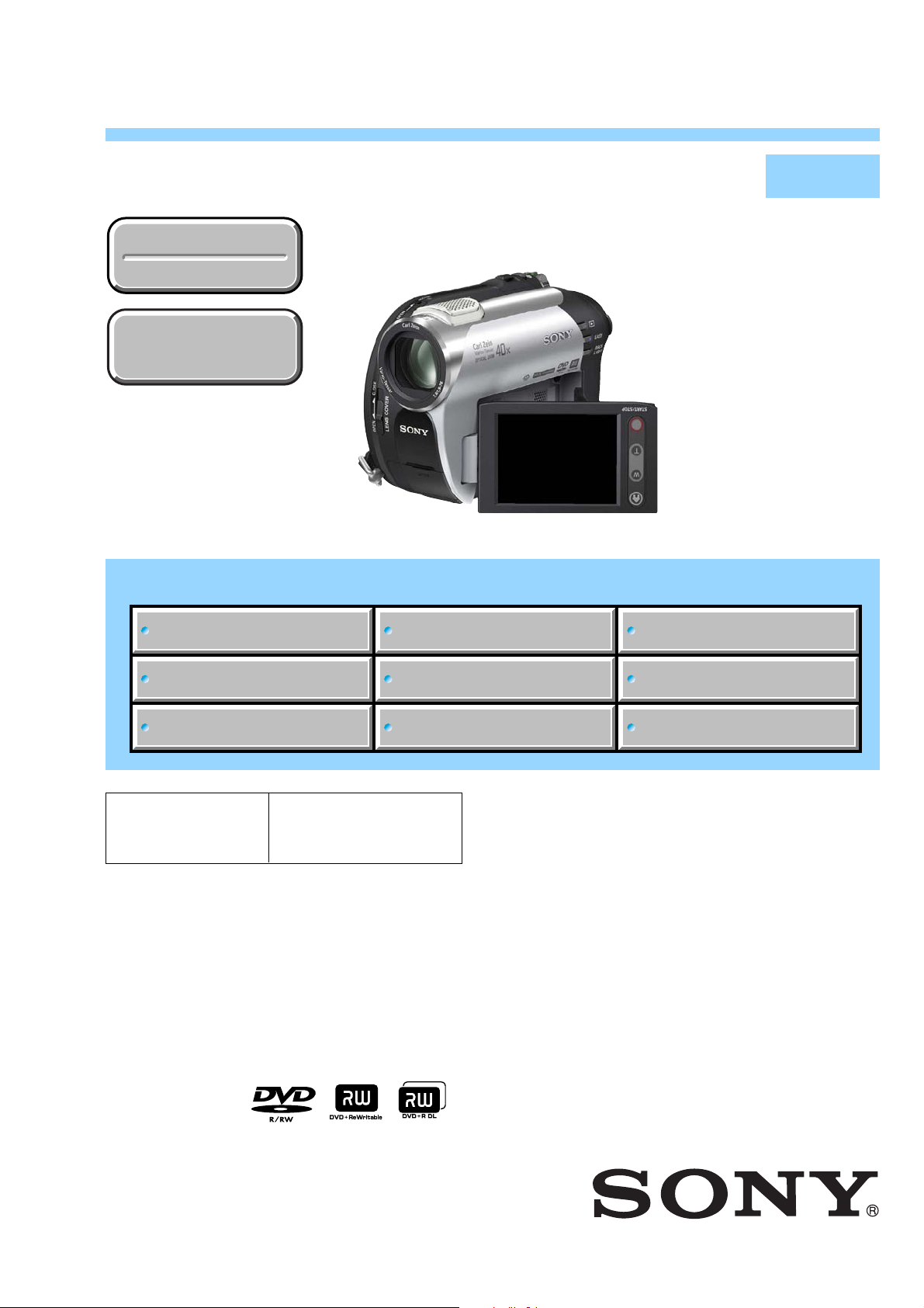
Photo: DCR-DVD108
Link
Link
SPECIFICATIONS
DISASSEMBLY
LEVEL 2
US Model
Canadian Model
AEP Model
UK Model
East European Model
North European Model
E Model
Australian Model
Hong Kong Model
Chinese Model
Argentine Model
Brazilian Model
SCHEMATIC DIAGRAMS
MODEL INFORMATION TABLE
SERVICE NOTE
The components identified by
mark 0 or dotted line with
mark 0 are critical for safety.
Replace only with part number specified.
BLOCK DIAGRAMS
FRAME SCHEMATIC DIAGRAM
Les composants identifiés par une
marque 0 sont critiques pour la
sécurité.
Ne les remplacer que par une pièce
portant le numéro spécifié.
PRINTED WIRING BOARDS
REPAIR PARTS LIST
DIGITAL VIDEO CAMERA RECORDER
DCR-DVD106E/DVD108/DVD108E/DVD109E/DVD608/DVD608E_L2
Sony EMCS Co.
2007G0500-1
© 2007.7
Published by Kohda TEC9-852-173-31

SPECIFICATIONS
System
Video compression format
MPEG2/JPEG (S till images)
Audio compression format
DCR-DVD106E/DVD108E/DVD608E
Dolby Digital 2ch
Dolby Digital Stereo Creator
DCR-DVD109E
Dolby Digital 2/5.1ch
Dolby Digital 5.1 Creator
Video signal
PAL color, CCIR standards
Usable discs
8 cm DVD-RW/D VD+RW/DVD-R/
DVD+R DL
Recording format
Movie
DVD-RW:DVD-VIDEO (VIDEO mode),
DVD+RW: DVD+RW Video
DVD-R/DVD+R DL: DVD-VIDEO
Still image
Exif
DVD-Video Recording
(VR mode)
*
Ver. 2.2
Recording time
DVD-RW/DVD+RW/DVD-R
HQ:Approx. 20 min
SP: Approx. 30 min
LP: Approx. 60 min
DVD+R DL
HQ:Approx. 35 min
SP: Approx. 55 min
LP:Approx. 110 min
Viewfinder
Electric viewfinder (color)
Image device
3 mm (1/6 type) CCD (Charge Coupled Device)
Gross:
Approx. 800 000 pixels
Effective (Movie):
Approx. 400 000 pixels
Effective (Still):
Approx. 400 000 pixels
Lens
Carl Zeiss Vario-Tessar
Optical:40×, Digital:80×, 2 000×
Focal length
F=1.8-4.1
f=1.9 - 76.0mm (3/32 - 3 in.)
When converted to a 35 mm still camera
For movies:
36 - 1 440mm (1 7/16 - 56 3/4 in.)
For still images:
36 - 1 440mm (1 7/16 - 56 3/4 in.)
Color temperature
[AUTO], [ONE PUSH], [INDOOR] (3 200 K),
[OUTDOOR] (5 800 K)
Minimum illumination
3 lx (lux) (AUTO SLW SHUTTR ON, Shutter
speed 1/25 second)
0 lx (lux) (during NightShot plus function)
*“Exif” is a file format for still images, established
by the JEIT A (Japan Electronics and Information
Technology Industries Association). Files in this
format can have additional information such as
your camcorder’s setting information at the time
of recording.
**In 16:9 mode, the focal length figures are actual
figures resulting from wide angle pixel readout.
• Manufactured under license from Dolby
Laboratories.
Input/Output connectors
Audio/Video output
10 pin connector
Video signal: 1 Vp-p, 75 Ω (ohms)
Luminance signal: 1 Vp-p, 75 Ω (ohms)
Chrominance signal: 0.3 Vp-p, 75 Ω (ohms)
Audio signal: 327 mV (at Load impedance
47 kΩ (kilohms)), Output impedance less than
2.2 kΩ (kilohms)
USB jack
mini-B
(DCR-DVD106E/DVD109E: output only)
LCD screen
Picture
6.2 cm (2.5 type)
Total number of pixels
123 200 (560 × 220)
General
Power requirements
6.8 V/7.2 V (battery pack)
8.4 V (AC Adaptor)
Average power consumption
DCR-DVD106E/DVD108E/DVD608E
LCD : 2.9W
Viewfinder : 2.7W
DCR-DVD109E
LCD : 3.0W
Viewfinder : 2.8W
Operating temperature
0°C to +40°C (32°F to 104°F)
Storage temperature
-20°C to +60°C (-4°F to +140°F)
Dimensions (Approx.)
54.5 × 89 × 130.5 mm (2 1/4 × 3 5/8 × 5 1/4
in.) (w × h × d) including the projecting parts
54.5 × 89 × 130.5 mm (2 1/4 × 3 5/8 × 5 1/4
in.) (w × h × d) including the projecting parts
with supplied battery pack NP-FH40 attached
Mass (Approx.)
390 g (13 oz) main unit only
440 g (15 oz) including the NP-FH40
rechargeable battery pack and disc
Supplied accessories
AC Adaptor (1)
Mains lead (1)
A/V connecting cable (1)
USB cable (1)
Rechargeable battery pack NP-FH40 (1)
CD-ROM “Handycam Application Software” (1)
Operating Guide (1)
See page 5-18.
AC Adaptor AC-L200/L200B
Power requirements
AC 100 - 240 V, 50/60 Hz
Current consumption
0.35 - 0.18 A
Power consumption
18W
Output voltage
DC 8.4V*
Operating temperature
0°C to +40°C (32°F to 104°F)
Storage temperature
-20°C to +60°C (-4°F to +140°F)
Dimensions (Approx.)
48 × 29 × 81 (1 15/16 × 1 3/16 × 3 1/4 in.)
(w × h × d) excluding the projecting parts
Mass (Approx.)
170 g (6 oz) excluding the mains lead
* See at the label of AC Adaptor for other
specifications.
Rechargeable battery pack NP-FH40
Maximum output voltage
DC8.4V
Output voltage
DC7.2V
Capacity
4.9 wh (680 mAh)
Dimensions (Approx.)
31.8 × 18.5 × 45.0 mm
(1 5/16 × 3/4 × 1 13/16 in.) (w × h × d)
Mass (Approx.)
45 g (1.6 oz)
Operating temp erature
0°C to +40°C (32°F to 104°F)
Type
Li-ion
Design and specifications are subject to change
without notice.
DCR-DVD106E/DVD108/DVD108E/DVD109E/DVD608/DVD608E_L2
— 2 —
Model information table
Model DCR-DVD106E DCR-DVD108 DCR-DVD108E
Destination AEP, UK, EE, NE US, CND, E, AR, BR NE
Color system PAL NTSC PAL
5.1ch recording ×××
CAM → PC aaa
Data
copy
PC → CAM × aa
Model DCR-DVD109E DCR-DVD608 DCR-DVD608E
Destination AEP, UK, EE, NE E E, HK, AUS, CH
Color system PAL NTSC PAL
5.1ch recording a ××
CAM → PC aaa
Data
copy
PC → CAM × aa
•Abbreviation
AR : Argentine model
AUS: Australian model
BR : Brazilian model
CH : Chinese model
CND: Canadian model
EE : East European model
HK : Hong Kong model
J: Japanese model
JE : Tourist model
KR : Korea model
MX : Mexican model
NE : North European model
DCR-DVD106E/DVD108/DVD108E/DVD109E/DVD608/DVD608E_L2
— 3 —

CAUTION :
Danger of explosion if battery is incorrectly replaced.
Replace only with the same or equivalent type.
WARNING!!
WHEN SERVICING, DO NOT APPROACH THE LASER
EXIT WITH THE EYE TOO CLOSELY. IN CASE IT IS
NECESSARY TO CONFIRM LASER BEAM EMISSION,
BE SURE T O OBSER VE FR OM A DISTANCE OF MORE
THAN 30 cm FROM THE SURFACE OF THE
OBJECTIVE LENS ON THE OPTICAL PICK-UP BLOCK.
CAUTION:
The use of optical instrument with this product will increase eye
hazard.
CAUTION
Use of controls or adjustments or performance
procedures other than those specified herein may
result in hazardous radiation exposure.
SAFETY-RELATED COMPONENT WARNING!!
COMPONENTS IDENTIFIED BY MARK 0 OR DO TTED LINE WITH
MARK 0 ON THE SCHEMATIC DIAGRAMS AND IN THE PARTS
LIST ARE CRITICAL TO SAFE OPERATION. REPLACE THESE
COMPONENTS WITH SONY PARTS WHOSE PART NUMBERS
APPEAR AS SHOWN IN THIS MANUAL OR IN SUPPLEMENTS
PUBLISHED BY SONY.
SAFETY CHECK-OUT
After correcting the original service problem, perform the following
safety checks before releasing the set to the customer.
1. Check the area of your repair for unsoldered or poorly-soldered
connections. Check the entire board surface for solder splashes
and bridges.
2. Check the interboard wiring to ensure that no wires are
"pinched" or contact high-wattage resistors.
3. Look for unauthorized replacement parts, particularly
transistors, that were installed during a previous repair. Point
them out to the customer and recommend their replacement.
4. Look for parts which, through functioning, show obvious signs
of deterioration. Point them out to the customer and
recommend their replacement.
5. Check the B+ voltage to see it is at the values specified.
6. Flexible Circuit Board Repairing
•Keep the temperature of the soldering iron around 270˚C
during repairing.
• Do not touch the soldering iron on the same conductor of the
circuit board (within 3 times).
• Be careful not to apply force on the conductor when soldering
or unsoldering.
ATTENTION AU COMPOSANT AYANT RAPPORT
À LA SÉCURITÉ!
LES COMPOSANTS IDENTIFÉS P AR UNE MARQUE 0 SUR LES
DIAGRAMMES SCHÉMA TIQ UES ET LA LISTE DES PIÈCES SONT
CRITIQUES POUR LA SÉCURITÉ DE FONCTIONNEMENT. NE
REMPLACER CES COMPOSANTS QUE PAR DES PIÈSES SONY
DONT LES NUMÉROS SONT DONNÉS DANS CE MANUEL OU
DANS LES SUPPÉMENTS PUBLIÉS PAR SONY.
Unleaded solder
Boards requiring use of unleaded solder are printed with the leadfree mark (LF) indicating the solder contains no lead.
(Caution: Some printed circuit boards may not come printed with
the lead free mark due to their particular size.)
: LEAD FREE MARK
Unleaded solder has the following characteristics.
• Unleaded solder melts at a temperature about 40°C higher than
ordinary solder.
Ordinary soldering irons can be used but the iron tip has to be
applied to the solder joint for a slightly longer time.
Soldering irons using a temperature regulator should be set to
about 350°C.
Caution: The printed pattern (copper foil) may peel away if the
heated tip is applied for too long, so be careful!
• Strong viscosity
Unleaded solder is more viscous (sticky , less prone to flow) than
ordinary solder so use caution not to let solder bridges occur such
as on IC pins, etc.
•Usable with ordinary solder
It is best to use only unleaded solder but unleaded solder may
also be added to ordinary solder.
DCR-DVD106E/DVD108/DVD108E/DVD109E/DVD608/DVD608E_L2
— 4 —

TABLE OF CONTENTS
Section Title Page
1. SERVICE NOTE
1-1. Power Supply During Repairs·········································1-1
1-2. To Take Out a Cassette when not Eject (Force Eject) ·····1-1
1-3. Using Service Jig·····························································1-2
1-4. Self-diagnosis Function ···················································1-2
2. DISASSEMBLY
2-1. Disassembly·····································································2-2
3. BLOCK DIAGRAMS
3-1. Overall Block Diagram (1/5)··········································· 3-1
3-2. Overall Block Diagram (2/5)··········································· 3-2
3-3. Overall Block Diagram (3/5)··········································· 3-3
3-4. Overall Block Diagram (4/5)··········································· 3-4
3-5. Overall Block Diagram (5/5)··········································· 3-5
3-6. Power Block Diagram (1/3)············································· 3-6
3-7. Power Block Diagram (2/3)············································· 3-7
3-8. Power Block Diagram (3/3)············································· 3-8
4. PRINTED WIRING BOARDS AND
SCHEMATIC DIAGRAMS
4-1. Frame Schematic Diagrams·············································4-1
4-2. Schematic Diagrams························································4-3
4-3. Printed Wiring Boards ···················································4-29
4-4. Mounted Parts Location ················································4-43
5. REPAIR PARTS LIST
5-1. Exploded V iews·······························································5-2
5-2. Electrical Parts List ·························································5-9
DCR-DVD106E/DVD108/DVD108E/DVD109E/DVD608/DVD608E_L2
— 5 —
1. SERVICE NOTE
1-1. POWER SUPPLY DURING REPAIRS
In this unit, about 10 seconds after power is supplied to the battery terminal using the regulated power supply (8.4 V), the power is shut off so
that the unit cannot operate.
These following method is available to prevent this.
Method:
Use the AC power adaptor (AC-L200/L200B).
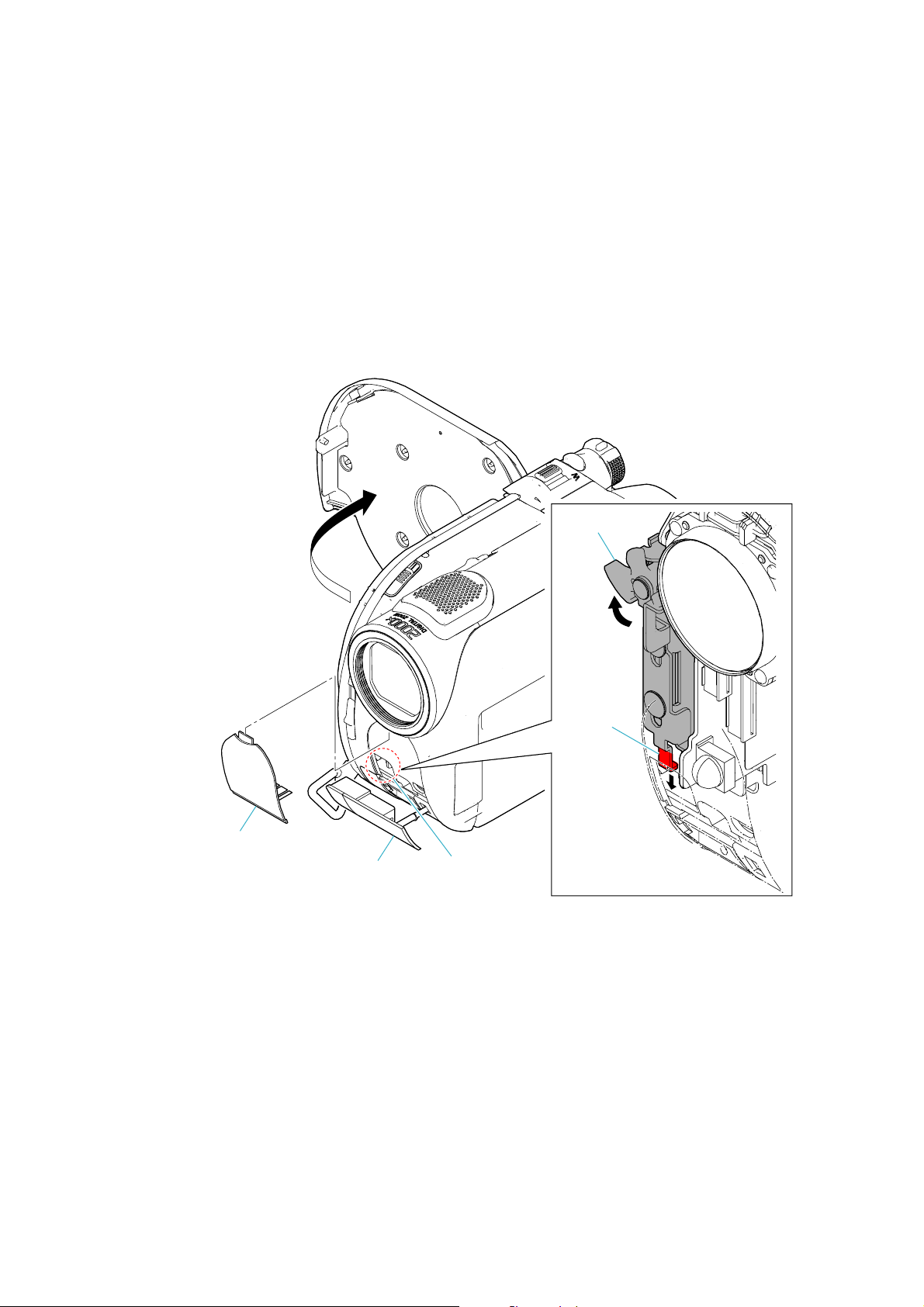
1-2. TO TAKE OUT A DISC WHEN NOT EJECT (FORCE EJECT)
1 Peel off the jack cover assy and remote control window.
2 Insert the wire etc. in the hole and down the eject slider by it.
Charge
lever
Remote control window
Jack cover assy
Eject slider
Hole
DCR-DVD106E/DVD108/DVD108E/DVD109E/DVD608/DVD608E_L2
1-1
1-3. USING SERVICE JIG
k
Connect the extension cable (J-6082-572-A) between the DVD mechanism deck and CN1008 on the VC-483 board.
VC-483 board (side B)
CN1008
Extension cable (10P)
(J-6082-572-A)
Flexible board (10P)
DVD mechanism dec
1-4. SELF-DIAGNOSIS FUNCTION
1-4-1. Self-diagnosis Function
When problems occur while the unit is operating, the self-diagnosis
function starts working, and displays on the viewfinder or LCD
screen what to do.
Details of the self-diagnosis functions are provided in the Instruction
manual.
Viewfinder or LCD screen
C : 3 1 : 1 1
Blinks at 3.2Hz
1 1
Repaired by:
C : Corrected by customer
H : Corrected by dealer
E : Corrected by service
engineer
3 1C
Block
Indicates the appropriate
step to be taken.
E.g.
31 ....Reload the tape.
32 ....Tur n o n power again.
1-4-2. Self-diagnosis Display
When problems occur while the unit is operating, the counter of the
viewfinder or LCD screen shows a 4-digit display consisting of an
alphabet and numbers, which blinks at 3.2 Hz. This 5-character
display indicates the “repaired by:”, “block” in which the problem
occurred, and “detailed code” of the problem.
Detailed Code
Refer to “1-4-3. Self-diagnosis Code Table”.
DCR-DVD106E/DVD108/DVD108E/DVD109E/DVD608/DVD608E_L2
1-2

1-4-3. Self-diagnosis Code Table
Self-diagnosis Code
Repaired by:
C
C
C
E
E
E
E
E
E
Block
Function
04
13
13
20
31
61
61
61
94
Detailed
Code
00
01
02
00
00
00
10
11
00
Symptom/State
Non-standard battery is used.
“Memory Stick Duo” is unformatted.
“Memory Stick Duo” is broken.
Disc access error
Flash memory data are rewritten.
Drive fault
Difficult to adjust focus
(Cannot initialize focus.)
Zoom operations fault
(Cannot initialize zoom lens.)
The abnormalities in initialization of
the focus lens and the abnormalities in
initialization of the zoom lens occurred
simultaneously.
Fault of writing to or erasing the flash
memory
Correction
Use the InfoLITHIUM battery.
Format the “Memory Stick Duo”.
Insert a new “Memory Stick Duo”.
Clean the disc with the supplied cleaning cloth.
Use a compatible disc with the camcorder.
Make flash memory data correct value. (Note)
Inspect or replacement of the mechanism deck, IC (IC4401 on
the VC-483 board) and drive block.
Inspect the lens block focus reset sensor (pin 7 of CN5601 on
the VC-483 board) when focusing is performed when the focus
buttons of the touch panel are pressed in the focus manual mode,
and the focus motor drive circuit (IC5601 on the VC-483 board)
when the focusing is not performed.
Inspect the lens block zoom reset sensor (pin qa of CN5601 on
the VC-483 board) when zooming is performed when the zoom
lever is operated, and the zoom motor drive circuit (IC5601 on
the VC-483 board) when zooming is not performed.
Check whether the flexible board of the lens is broken, and
check whether it is inserted imperfectly. If there is no problem in
the flexible board, inspect the focus/zoom motor drive circuit
(IC5601 on the VC-483 board).
Inspect the flash memory (IC2201 on the VC-483 board). (Note)
Note: Refer to “1-3. DESTINATION DATA WRITE”, ADJ (9-852-173-51).
DCR-DVD106E/DVD108/DVD108E/DVD109E/DVD608/DVD608E_L2
1-3E

NOTE FOR REPAIR
2. DISASSEMBLY
• Make sure that the flat cable and flexible board are not cracked of bent at the terminal.
Do not insert the cable insufficiently nor crookedly.
• When remove a connector, don’t pull at wire of connector. It is possible that a wire is snapped.
• When installing a connector, don’t press down at wire of connector.
It is possible that a wire is snapped.
Cut and remove the part of gilt
which comes off at the point.
(Be careful or some
pieces of gilt may be left inside)
DCR-DVD106E/DVD108/DVD108E/DVD109E/DVD608/DVD608E_L2
2-1
HELP
EXPLODED VIEW
HELP
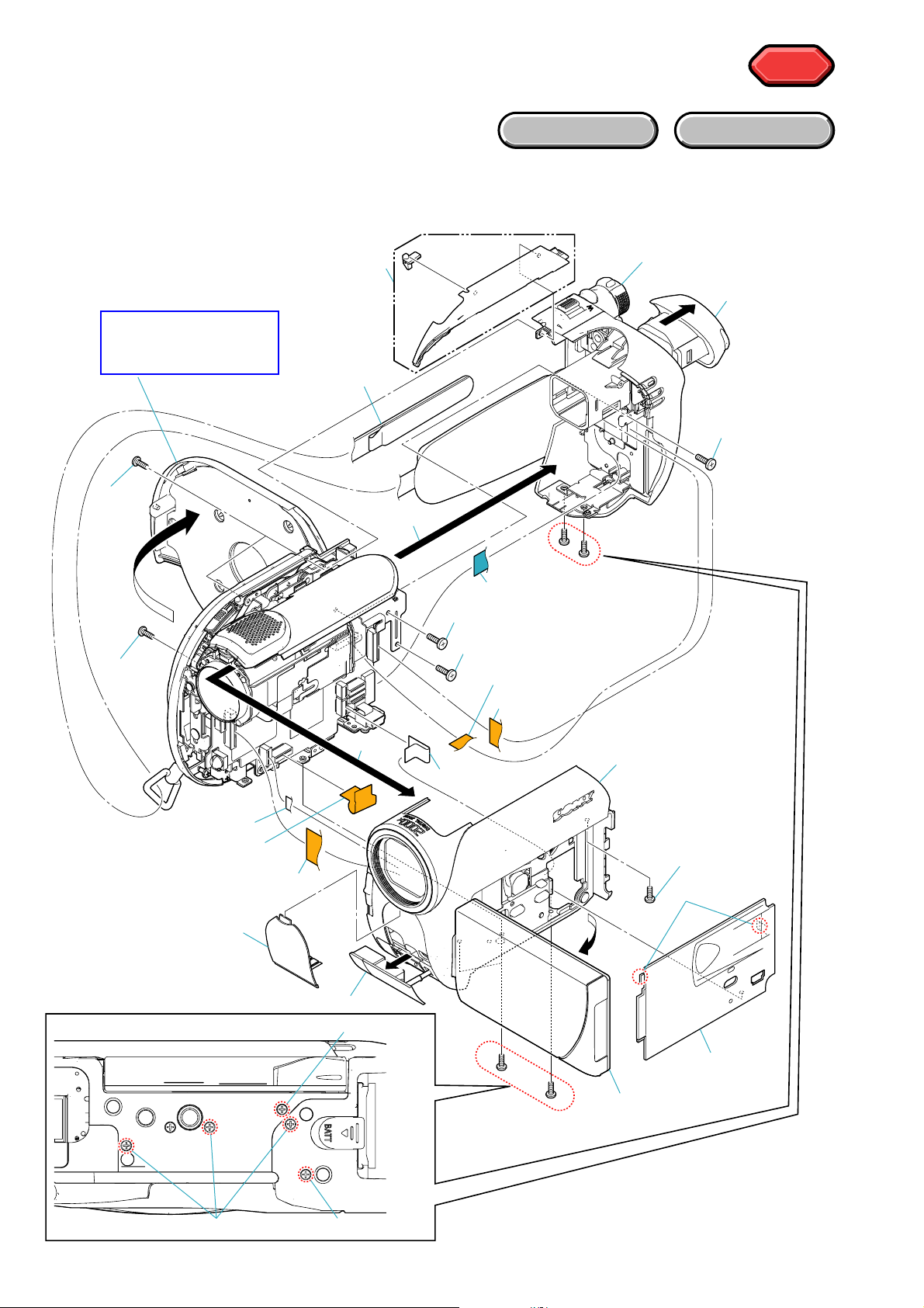
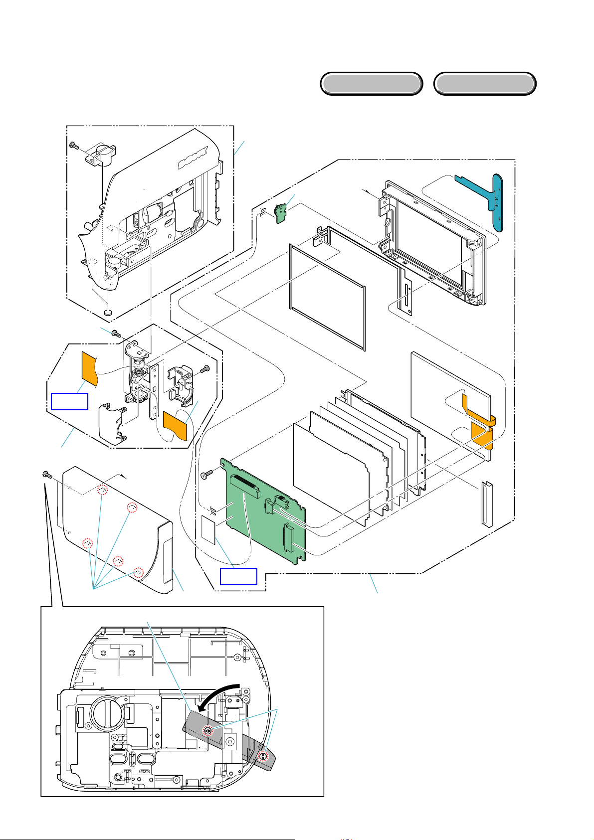
2-1. DISASSEMBLY
2-1-1. OVERALL SECTION
Follow the disassembly in the numerical order given.
1 Cabinet (R) Section (1-1 to 1-17)
2 BT-EVF Block (2-1 to 2-10)
1-10 (Open)
Refer to page 1-1 “1-2.
To take out a disk when
not eject (force eject)”.
1-12
(#11)
2-10
1-1
HARDWARE LIST
2 BT-EVF Block
2-6 (Pull)
2-7 (#2)
2-8
1-11 (#2)
1-14
1-15
1-9
1-17
1-8 (Pull)
1-16
1-3 (#2)
2-4 (#11)
2-5 (#2)
1-13
2-9
2-1
2-2
1 Cabinet (R)
Section
1-7 (#2)
1-4 (Claw)
1-6 (#2)
DCR-DVD106E/DVD108/DVD108E/DVD109E/DVD608/DVD608E_L2
1-5
1-2 (Open)
2-3 (#2)
2-2
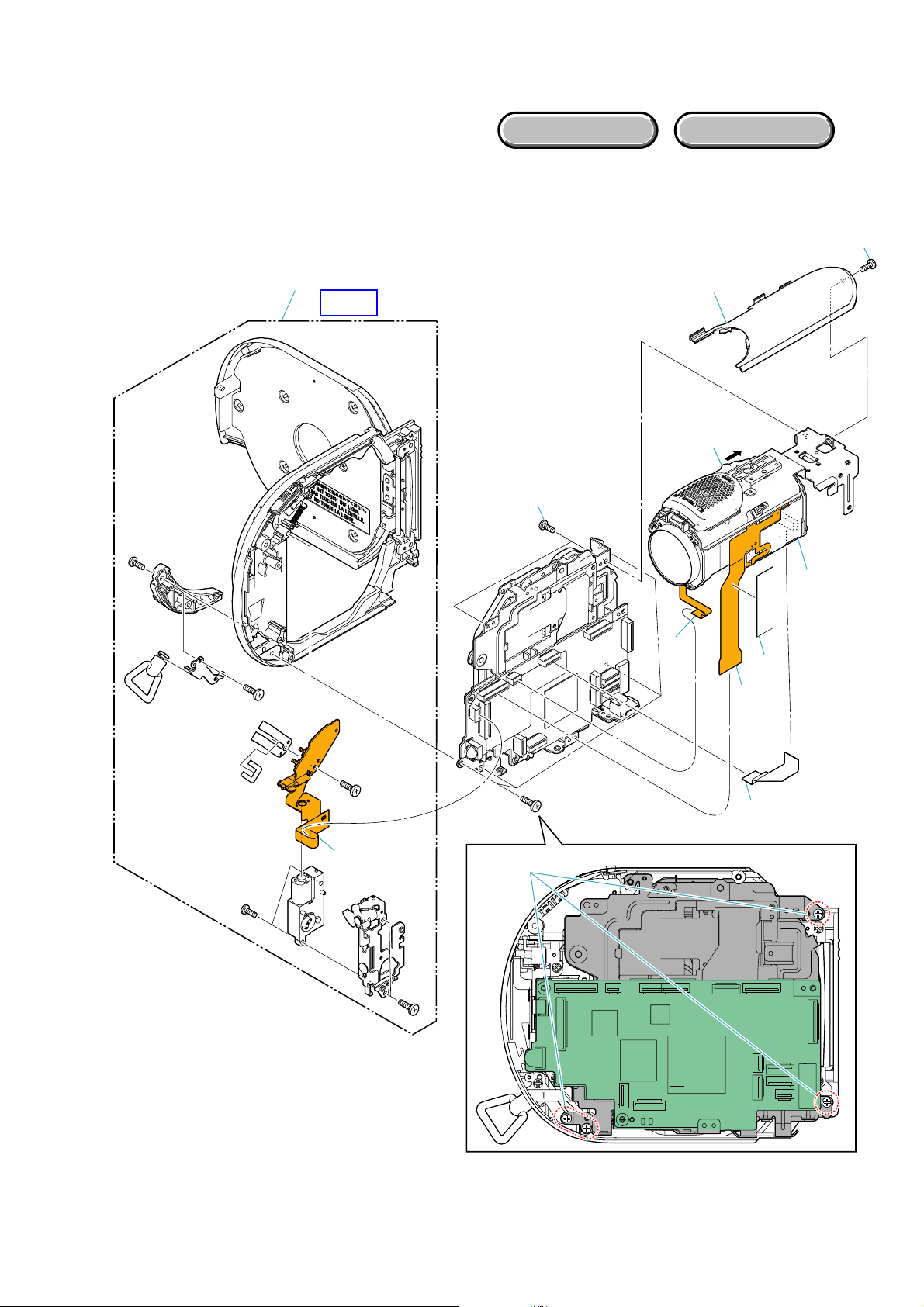
2-1-2. CABINET (L) SECTION
EXPLODED VIEW
Follow the disassembly in the numerical order given.
1 Upper Cabinet (1-1 to 1-2)
2 Cabinet L Assy (2-1 to 2-2)
3 Lens Block (3-1 to 3-5)
HARDWARE LIST
1-2 (#1)
2 Cabinet L Assy
HELP
1 Upper Cabinet
1-1
(Pull the Switch)
3-5 (#3)
3 Lens
Block
3-3
3-1
3-2
DCR-DVD106E/DVD108/DVD108E/DVD109E/DVD608/DVD608E_L2
2-1
3-4
2-2 (#11)
2-3
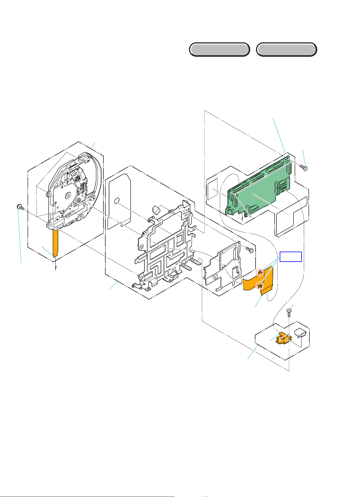
2-1-3. MD BLOCK
EXPLODED VIEW
Follow the disassembly in the numerical order given.
1 FP-574 Flexible Board (1-1 to 1-2)
2 VC-483 Board (2-1 to 2-3)
3 Mechanism Deck (3-1 to 3-3)
HARDWARE LIST
2 VC-483 Board
2-3
3-1 (#16)
3 Mechanism Deck
3-3
2-2
2-1
(#3)
VC-483
3-2
HELP
1-1
(#3)
DCR-DVD106E/DVD108/DVD108E/DVD109E/DVD608/DVD608E_L2
1-2
1 FP-574 Flexible Board
2-4
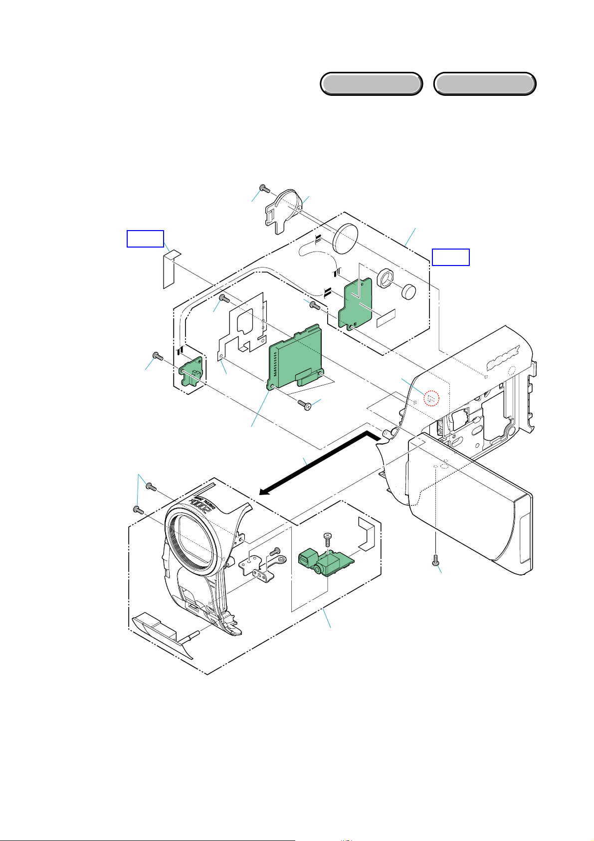
2-1-4. CABINET (R) SECTION
EXPLODED VIEW
Follow the disassembly in the numerical order given.
1 Front Panel Block (1-1 to 1-3)
2 MS-358 Board (2-1 to 2-5)
3 OC-001/CK-170 Board (3-1 to 3-4)
3-1 (#11)
HARDWARE LIST
3-2
2-1
HELP
3-4 (#11)
1-2 (#11)
2-2
(#11)
2-5
2 MS-358
Board
3-3
(#11)
MS-358
1-3
3 OC-001/CK-170
Board
HELP
CK170
2-3
(Claw)
2-4
(#3)
DCR-DVD106E/DVD108/DVD108E/DVD109E/DVD608/DVD608E_L2
1-1 (#2)
1 Front Panel Block
2-5
2-1-5. LCD BLOCK
EXPLODED VIEW
Follow the disassembly in the numerical order given.
1 LCD Panel Block (1-1 to 1-6)
2 Hinge Assy (2-1 to 2-2)
2-1 (#11)
HARDWARE LIST
2-2
1-6
HELP
2 Hinge Assy
1-3 (Claw)
1-1 (Turn)
1-4
1-5
PD-314
HELP
1 LCD Panel Block
DCR-DVD106E/DVD108/DVD108E/DVD109E/DVD608/DVD608E_L2
1-2 (#2)
2-6E
HELP
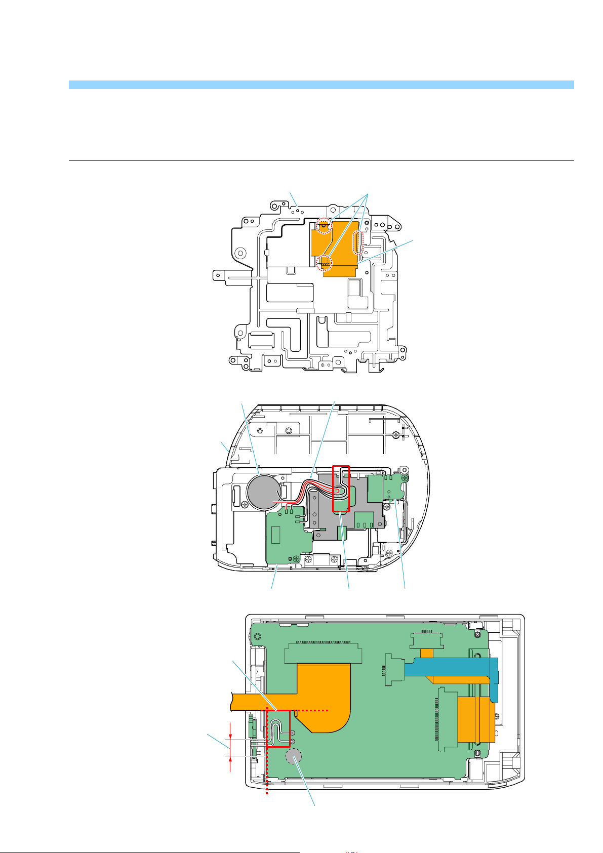
Sheet attachment positions and procedures of processing the flexible boards/harnesses are shown.
Loud speaker
Cabinet (R) section
MD frame assy
Hook
Mechanism deck
flexible board
Harness arrangement
CK-170 board Tape (A) OC-001 board
Tape (P)
Draw around the harness
within this area.
DCR-DVD106E/DVD108/DVD108E/DVD109E/DVD608/DVD608E_L2
PD-314 Board
Put neither the harness nor the tape in this area.
HELP
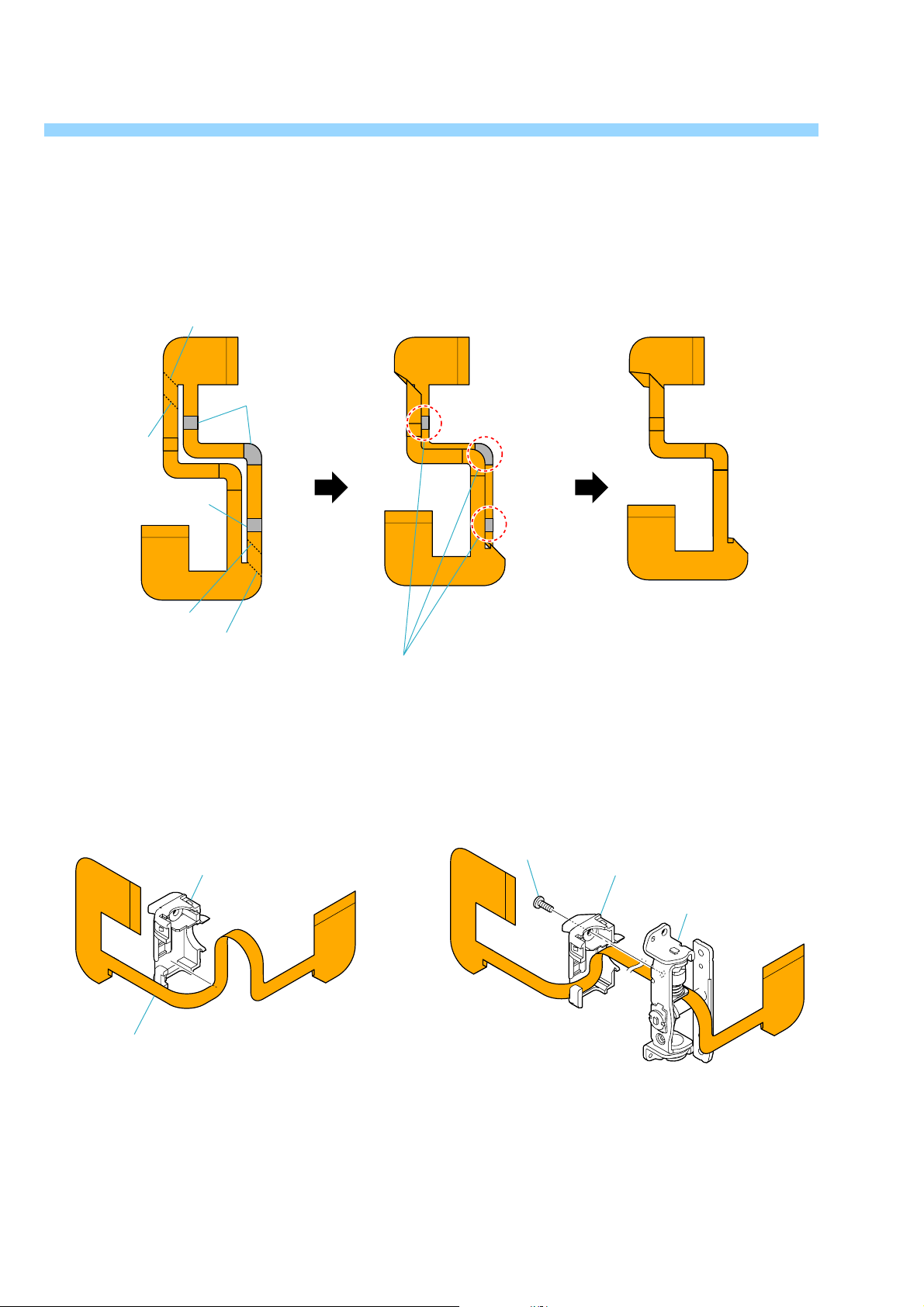
THE METHOD OF ATTACHMENT OF FP-573 FLEXIBLE BOARD
1 Fold dotted line parts of the FP-573 flexible board
as shown in figure.
Valley fold
Adhesive tape
Mountain
fold
Adhesive tape
Valley fold
Mountain fold
Stick it together in the adhesive tape
while bending the FP-573 flexible board.
2 Put the FP-573 flexible board on the
hinge cover (M).
Hinge cover (M)
FP-625 flexible board
3 Fix hinge cover (M) and the panel hinge assy (M)
with the screw.
Screw
Hinge cover (M)
Panel hinge assy (M)
DCR-DVD106E/DVD108/DVD108E/DVD109E/DVD608/DVD608E_L2
HELP
4 Install the hinge cover (C) in the hinge cover (M).
Hinge cover (M)
Claw
Hinge cover (C)
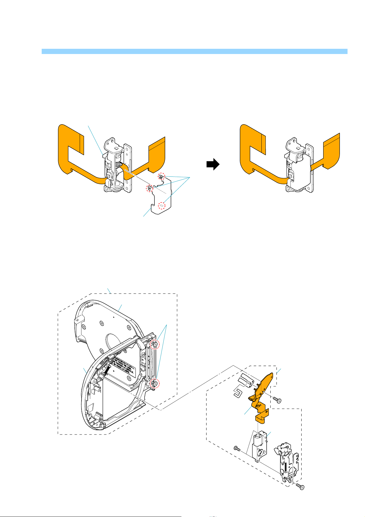
PRECAUTION WHEN INSTALLING THE CABINET L ASSY FOR SERVICE
Cabinet L assy for service
Cabinet D
block
D lid block
Screws
When the eject block is installed on the cabinet L assy
for service, a discrepancy could be made between the
cabinet D block and the D lid block, and as a result,
the D lid may not to be closed.
In case of such discrepancy, loosen the screws on the
hinge to eliminate the discrepancy of the D lid block,
and then retighten the screws.
Eject block
FP-569 flexible
complete board
M903
DCR-DVD106E/DVD108/DVD108E/DVD109E/DVD608/DVD608E_L2
HELP

Link
Link
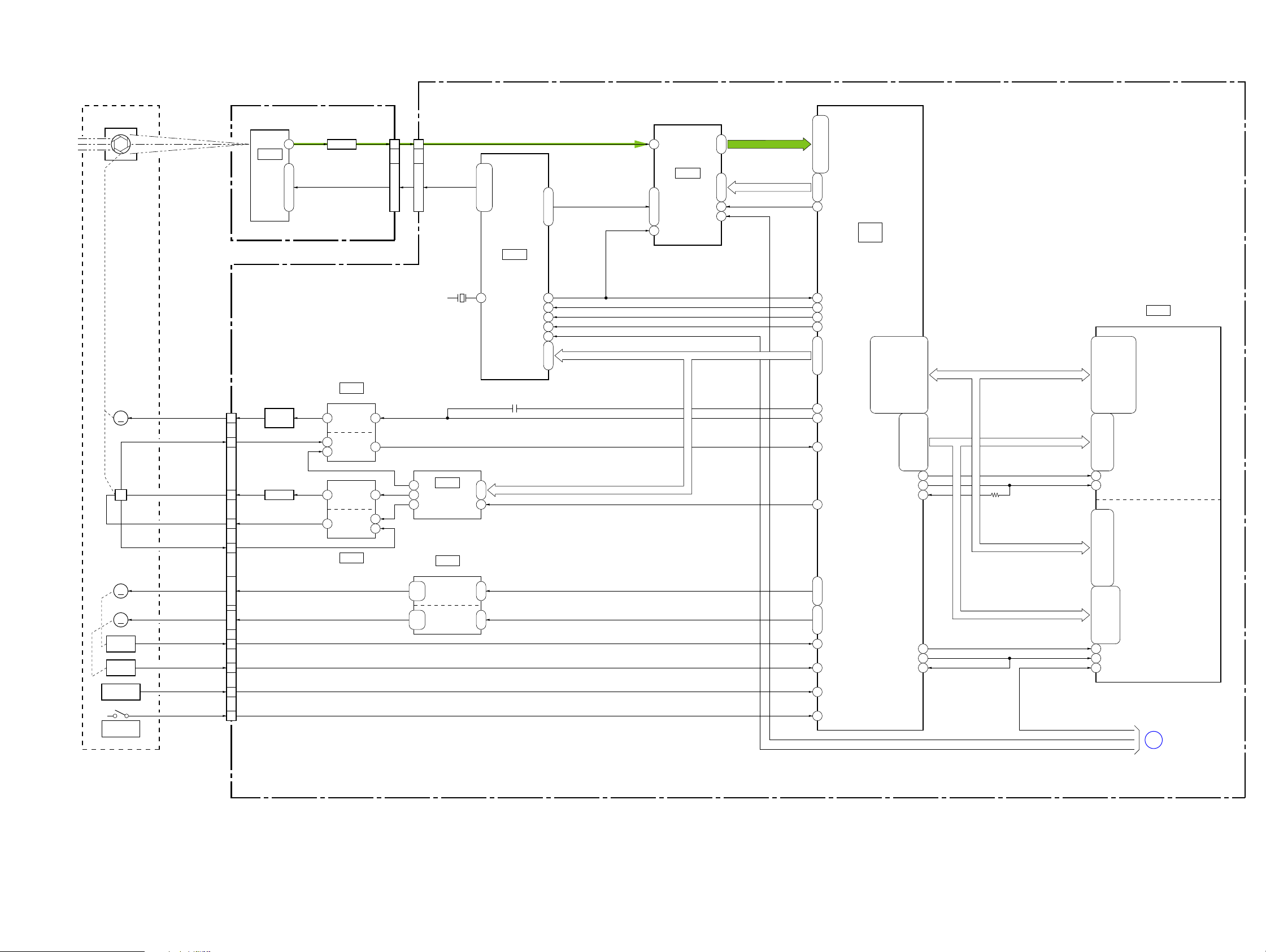
3. BLOCK DIAGRAMS
OVERALL BLOCK DIAGRAM (1/5)
OVERALL BLOCK DIAGRAM (2/5)
OVERALL BLOCK DIAGRAM (3/5)
OVERALL BLOCK DIAGRAM (4/5)
OVERALL BLOCK DIAGRAM (5/5)
POWER BLOCK DIAGRAM (1/3)
POWER BLOCK DIAGRAM (2/3)
POWER BLOCK DIAGRAM (3/3)
DCR-DVD106E/DVD108/DVD108E/DVD109E/DVD608/DVD608E_L2
3. BLOCK DIAGRAMS
3-1. O VERALL BLOCK DIAGRAM (1/5) ( ) : Number in parenthesis ( ) indicates the division number of schematic diagram where the component is located.
LENS BLOCK
IRIS
(SHUTTER)
IRIS
METER
M
H
FOCUS
MOTOR
M
ZOOM
MOTOR
M
FOCUS
SENSOR
ZOOM
SENSOR
LENS TEMP
SENSOR
NIGHTSHOT
PLUS
I_DRIVE (-)
I_HALL (-)
I_BIAS (-)
I_BIAS (+)
I_HALL (+)
FC_XA, FC_A,
FC_XB, FC_B
ZM_A, ZM_XA,
ZM_XB, ZM_B
FC_SENSE_OUT
ZM_SENSE_OUT
THERMO_OUT
IR_SWITCH_OUT
CD-686 BOARD
IC7101
IMAGER
CN5601
13
18
17
15
16
21 - 241 - 4
7
11
6
19
CCD
Q5601
IRIS
DRIVE
Q5603
AMP
7
4 - 1, 9, 10, 12, 13
BUFFER
V1 - V4, RG, VSHT, H1, H2
5
6
7
1
Q7101
IC5602
(2/17)
IRIS DRIVE
HALL AMP
HALL GAIN
HALL BIAS
IC5603
(2/17)
CN7101
31
7
5
3
2
VC-483 BOARD (1/5)
CN1601
8
7
9 - 12, 2, 1, 4, 5
6 - 3, 13, 14, 11, 10
A_2.8V
1
2
(D/A CONVERTER)
3
21, 4
23, 2,
17, 7
5, 19,
IC5604
EVR
(2/17)
IC5601
(2/17)
FOCUS
MOTOR
DRIVE
ZOOM
MOTOR
DRIVE
X1601
48MHz
9, 45, 12, 13
42, 40, 44, 41,
IC1601
TIMING
GENERATOR
(1/17)
CAM_SO, CAM_SCK
6, 7
DA_STRB
8
13 - 16 9 - 12
CCD_OUT+
PBLK, XSHP, XSHD, CLPDM
21, 16, 17, 22
VCK
2427
TG_HD
33
TG_VD
34
TG_FLD
35
CAM_DD_ON
6
CAM_SI, CAM_CS, CAM_SO, CAM_SCK
47, 3 - 1
DIR0A, DIR0B, EN0
DIR1A, DIR1B, EN01
30
19, 21 - 23
VCK
16
IRIS_COM
IRIS_PWM
I_HALL_AD
FC_RST
ZM_RST
LENS_TEMP_AD
XNS_SW
IC1602
S/H, AGC,
A/D CONVERTER
(1/17)
AD4 - AD13
2 - 11
CH_CS, CH_SO, CH_SCK
46 - 48
CLPOB
20
XSYS_RST
43
CAM_DD_ON
XSYS_RST
B13, C13, D11, B12, B11
D12, A13, D13, C12, A12,
M17, L16, L17
D8
IC2101
(1/5)
CPU
(3/17 - 5/17)
D9
D10
B10
C10
G17, H17, K17, J17
W2
W1
AK34
G10
N7, K8, M7
L9, J8, L8
AE32
A5
AL35
C6
AJ22, AJ25, AH23, AJ26,
AJ23, AF26, AH21, AG25,
AE19, AJ19, AF20, AG18
AE18, AJ20, AF19, AH18,
AE20, AH20, AH19, AF18,
AJ24, AG20, AH25, AD19,
AD18, AJ21, AH26, AG19,
AH24, AG21, AG26, AH22,
Y11, T10, V9, V10,
T11, W11, Y10, Y8
V11, W10, W12, Y9,
AA9, U12, V12, U11,
AF10
W25
W26
AF10
Y25
Y26
EMC_DATA [0] - EMC_DATA [31]
EMC_ADDR [0] - EMC_ADDR [12],
EMC_ADDR [14], EMC_ADDR [15]
EMC_XCS [1]
EMC_CLK0_OUT
EMC_DATA [0] - EMC_DATA [15]
EMC_ADDR [0] - EMC_ADDR [15]
EMC_XCS [0]
EMC_CLK1_OUT
XFLASH_RST
A : VIDEO SIGNAL
G5, G4, F5, G2, G3
P5, N5, N4, J4, H5, H4,
D13, P2, P3, N2, N3, P4,
G11, G10, F11, E13, E12,
M11, L10, L11, H11, H10,
R12, P12, P13, N11, M10,
D4, F4, E4, E3, D3,
R5, R4, T3, R3, E2,
J13
K11
T11, U11, U6, R7, R8,
V5, T6, P8, P9, R9, R10,
F6, C4, D5, C5,
E6, D6, C6, E7,
U3
T4
E8
XFLASH_RST
XSYS_RST
CAM_DD_ON
512M SDRAM
P6, E5, K5, L4, L5
P10, T9, R11, T12, U12,
512M OneNAND FLASH
C11, B11, D11, E9
C10, B10, D10, F8,
IC2201
(6/17)
1
OVERALL (5/5)
(PAGE 3-5)
05
DCR-DVD106E/DVD108/DVD108E/DVD109E/DVD608/DVD608E_L2
3-1
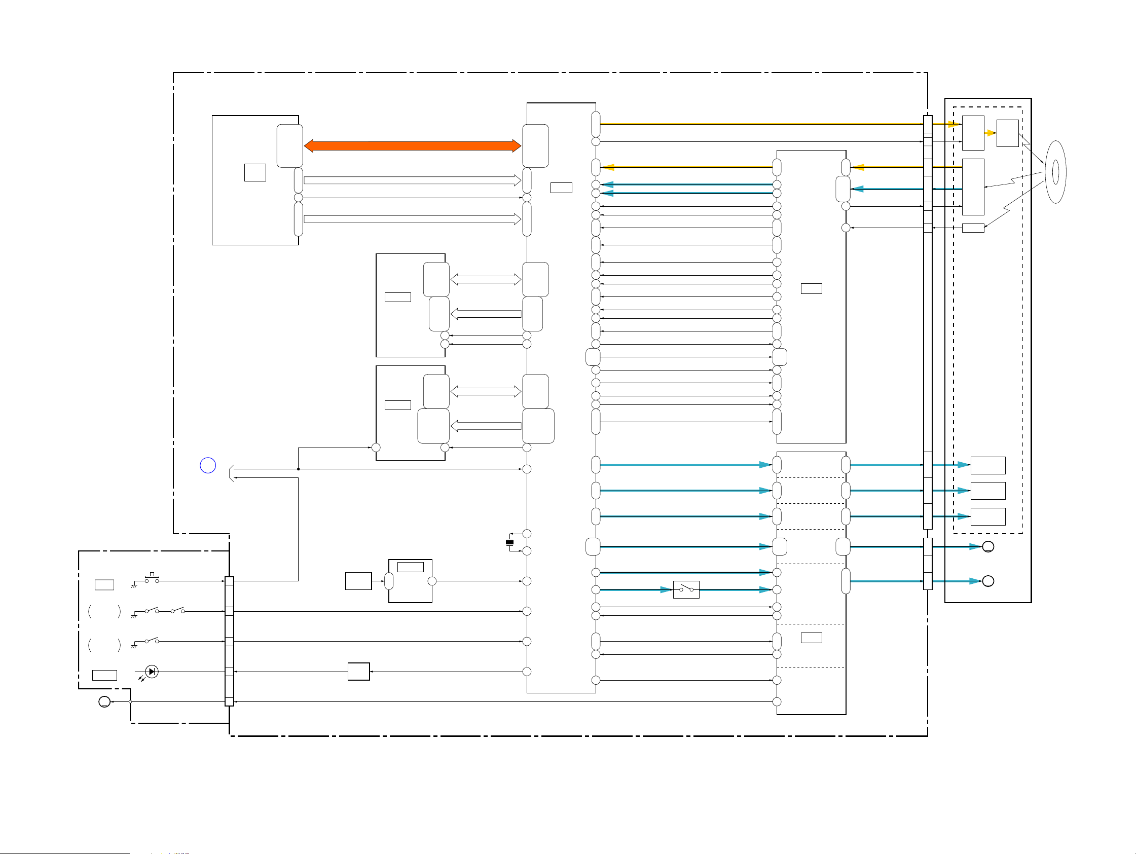
3-2. O VERALL BLOCK DIAGRAM (2/5)
( ) : Number in parenthesis ( ) indicates the division number of schematic diagram where the component is located.
FP-569 FLEXIBLE BOARD
S5691
OPEN
LID OPEN
DETECT
S5693 S5692
VC-483 BOARD (2/5)
(3/17 - 5/17)
2
OVERALL (5/5)
(PAGE 3-5)
XEJECT_SW
LID_OPEN
5
6
CN1001
IC2101
(2/5)
CPU
XEJECT_SW
AJ8, AJ10, AM12, AJ9
AH11, AJ11, AJ13, AH9,
AJ14, AH8, AH13, AH10,
AH12, AH14, AJ12, AN12,
AM9 - AM11
TXD_TO_IC_4201, RXD_TO_IC_4201, XSCK_IC_4201, XCS_IC_4201
G19, H18, G18, H19
XIC_4201_RESET_FLASH
SE4501
SHOCK
SENSOR
ATA_D0 - ATA_D15
ATA_A0 - ATA_A2
XATA_RESET
IC4303
64M SDRAM
(8/17)
IC4302
16M FLASH
(8/17)
B4
2, 3
IC4501
SHOCK
SENSOR
AMP
(7/17)
50, 51, 53
2, 4, 5, 7, 8,
10, 11, 13, 42,
44, 45, 47, 48,
33, 34, 22, 35
23, 24, 25, 26,
29, 30, 31, 32,
19
38
F4, G5, F5, G6
F2, G2, F3, G3,
E2, H2, E3, H3,
H4, E4, H5, E5,
E6, B2, C3, D4
E1, D1, C1, A1,
B1, D2, C2, A2,
B5, A5, C5, D5,
B6, A6, C6, D6,
F1
10
SDDQ0 - SDDQ15
SDA0 - SDA11
XSDCS
SDCLK
FDQ0 - FDQ15
FEA0 - FEA19
FCE1Z
XIC_4201_RESETXIC_4201_RESET
X4201
33.8688MHz
GSHCK
LID_OPEN
P20, P21, P23, R22,
L22, L20, M22, N21,
R21, P22, N20, N22,
M21, M20, L21, R20
IC4201
H21, J21, H22
R23AL4
DVD DSP,
DVD DRIVE
CONTROL
(7/17)
D13, B13, C13, B14
D20, F21, F22, E23
F20, E20, D23, C23,
C21, A22, B23, C22,
D22, D21, E22, B22,
D17, C18, B17, D18
C17, C16, D15, B15,
A14, C15, B16, D16,
B19
A16
Y21, W20, V20, U22
AA22, Y23, W21, V21,
Y19, Y16, AA20, AB22,
AB19, AB21, AC22, AA21,
U20, U21, T23, T20,
T22, AB20, Y20, Y22
W23, W22, V23, V22,
AA16, Y17, AC18, Y18,
AC19, AC21, AB18, AA19,
AA17
AA13
AC12
AC13
A2
C12
Y5, AB5, AA5
Y12
MPXOUT1, MPXOUT2
N2, P4K2, K3B2, T4
FE
K4
TE
L4
PI
J4
CE
L1
PH1, PH2
J2, P1
BH1, BH2
J3, N3
VC
SWRF
R1
EQRF_S
H1 A8
RECD1
AWBL
U2
DWBL
AB2
LPP, LPP2
AA3, AA8
ATTPLS
AB6
MSPDSH, WFPDSF, ROPCSH, RFPDSH
Y6, AA4,
AB4, AB3
RFMCLK
B1 M4
WLDON
AB8
APCLOAD
Y8 H2
XRST_IC_4101
AC7
SDAT, SCS, SCLK
Y7, AA6, AB7
FFDR, FRDR
C8, D7
TFDR, TRDR
A6, C7
FMPWN_OUT0, FMPWN_OUT1
C4, C3
SLSTFD1, SLSTRD1, SLSTFD2, SLSTRD2
A5, C6
B7, D6,
SP_SPFD
SP_SPRD
SV_FS4SV
FGINI
Q4401
G11, H12
C12
D11
C11
E11
B11, A12
B12, A11
M1
H11
M9
J12
L9
M10, L10
L2
L3, L4,
M2, M3
L11, M11
L8
L6, L7, M6
E5, H6
G6, H7
G7, H8B4, C4
E4, F2,
G1, G2
B5B3
B3D4
A4B6
B7D5
IC4101
RF PROCESS
(9/17)
FOCUS
DRIVE
TRACKING
DRIVE
TILT
DRIVE
SLED
MOTOR
DRIVE
SPINDLE
MOTOR
DRIVE
LDD_W1DIS - LDD_W3DISWP1_OP - WP3_OP
B1, C1
F2, G1, G2, H1
D2, E1, E2, F1,
C2
C7, D5
D6, D7
E7, F6
G5, F5
G4, F4,
C3, D3, E1
CN4101
ENBLLD_EN
RF±
A - H
PDIC_GAIN
FPDIC_OUT
FCS±
TRK±
TLT±
CN1008
SLED1 - SLED4
U, V, W
DVD MECHANISM DECK
(DDX-C2000)
3 - 127, 2625 - 18
12
30
50
37 - 3441 - 3845 - 42
9 - 63 - 5
LD
DRIVE
PD IC
FPD ICA2
SLED MOTOR
SPINDLE MOTOR
FOCUS
COIL
TRACKING
COIL
TILT COIL
M
M
LASER
DIODE
S5694
EJECT
DETECT
D5691
ACCESS
M
M903
MOTOR UNIT
(GEARD MOTOR)
EJECT_DET
EJECT_DRV
8
1
3
05
DCR-DVD106E/DVD108/DVD108E/DVD109E/DVD608/DVD608E_L2
Q1004
LED
DRIVE
EJECT_DET
ACCS_LEDACCS_LED
D12
Y11
3-2
AB11, AA11
C11
B12
XMUTE0, XMUTE1
DRV_SEL
PLG
DVD MECHA DRIVE
B8
H1
F3
IC4401
(10/17)
EJECT
MOTOR
DRIVE
A : VIDEO/AUDIO/SERVO SIGNAL
A : VIDEO/AUDIO SIGNAL
A : SERVO SIGNAL
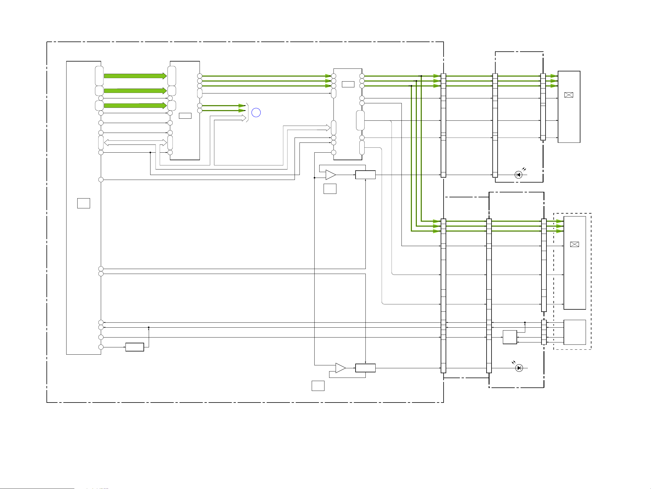
3-3. O VERALL BLOCK DIAGRAM (3/5)
VC-483 BOARD (3/5)
( ) : Number in parenthesis ( ) indicates the division number of schematic diagram where the component is located.
BL-006 BOARD
IC2101
(3/5)
CPU
(3/17 - 5/17)
DR_VDATA0 – DR_VDATA7
D32, C34, B33, C33
D35, E34, D33, D34,
DR_GHDATA0 – DR_GHDATA3
E33, F33
E32, G33,
H35 B15
F32, F34
G32, G34,
G35 D12
F35
U27
L18, M19, M18
G20
XCS_LCD
T27
DR_GHPILOT
DR_GSDATA0 – DR_GSDATA3
DR_GSPILOT
DR_VINCK
XCS_IC_2901
BB_SI, BB_SO, XBB_SCK
XBB_RST
E21
H2
J21
A18, B19, A20, B21
B17, A17, D18, B18,
A15, A14
B16, A16,
D13, A13
D14, B14,
IC2901
D/A
CONVERTER
(11/17)
J1, G2, H1
AA2
AA4
AA5
K1, K2
AA9
AA11
IC_2901_Y_OUT
IC_2901_C_OUT
BB_SO, XBB_SCK
3
OVERALL (4/5)
(PAGE 3-4)
PANEL_R
PANEL_G
PANEL_B
PANEL_HD, PANEL_VD
BB_SI, BB_SO, XBB_SCK
XCS_LCD
XBB_RST
EXTDA
34
33
32
42, 45, 44 48, 1
43
3
31
6
–
7
5
+
IC3702
(2/2)
EVF BACKLIGHT
CONTROL
(13/17)
IC3701
LCD/EVF
DRIVE
(13/17)
20
21
22
26
28
6 - 9, 12, 14,
16, 17, 30, 24
10
5, 11, 18
Q3706
BACKLIGHT
DRIVE
CN3701
CN3702
(1/2)
15
14
13
17
7
20
1
2
3
EVF_COM
EVF_HST, EVF_HCK1,
EVF_HCK2, EVF_BLK,
EVF_VCK, EVF_PCG,
EVF_REF, EVF_VST,
EVF_EN, EVF_PSIG
3 - 6, 8 - 12, 16
EVF_STB
FP-573 FLEXIBLE
BOARD (1/2)
PANEL_VR
PANEL_VG
PANEL_VB
EVF_VR
EVF_VG
EVF_VB
LED_K
CN5901
6
7
8
4
14
1
COM, CS
HST, HCK1, HCK2, BLK,
VCK, PCG, REF, VST,
EN, PSIG
18 - 15, 13 - 9, 5
D5902
(BACKLIGHT)
PD-314 BOARD (1/2)
CN6401
(1/2)
30
29
28
VR
VG
VB
STB
CN5902
CN6405
R
G
B
17
18
16
11
LCD902
21, 19
5 - 7, 9, 10, 12 - 15, 20
4
5
3
COLOR
EVF
UNIT
LCD901
30 1
EVF_BL_ON
D26
PANEL_BL_ON
Y4
TP_X
AM35
TP_Y
AN34
TP_SEL1
B29
TP_SEL2
B28
05
Q2101
TP SELECT
SWITCH
IC3702
(1/2)
EVF_BL_ON
PANEL_BL_ON
3
+
2
–
LCD BACKLIGHT
CONTROL
(13/17)
1
BACKLIGHT
DRIVE
Q3710 - Q3713
7, 17, 19 - 24, 28, 29
27 - 25
14
16
15
11 - 9
COM
WIDE, REF, HCK1, HCK2,
HST, PCG, EN, PSIG,
VST, VCK
24, 14, 12 - 7, 3, 2
RGT, DWN, XSTBY RGT, DWN, XSTBY
TP_X
TP_Y
TP_SEL1
BL_H1 - BL_H3
17
15
16
4 - 6
20 - 22
TOUCH
PANEL
I/F
Q6401, Q6402
A : VIDEO SIGNAL
COM, CS
PSIG, HCK1, HCK2,
WIDE, REF, HST,
PCG, EN, VCK, VST
CN6404
TP_TOP
TP_L
TP_R
TP_BOT
D6403 – D6405
(BACKLIGHT)
24, 23
6 - 9, 11 - 13, 20 - 22
2, 19, 14
3
5
2
6
2.5 inch
COLOR
LCD
UNIT
TOUCH
PANEL
DCR-DVD106E/DVD108/DVD108E/DVD109E/DVD608/DVD608E_L2
3-3
 Loading...