

Page 1
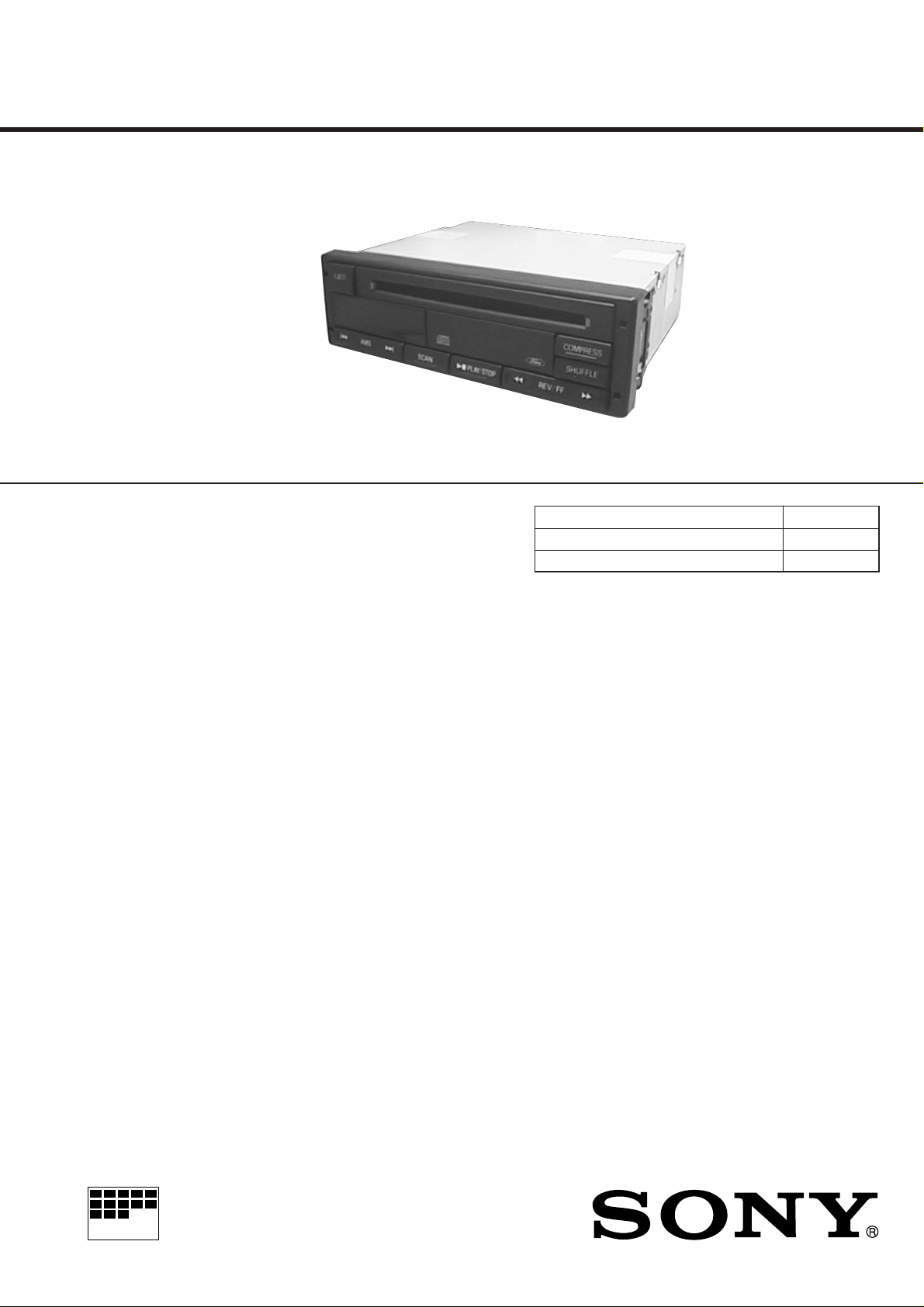
XR3F-19B160
SERVICE MANUAL
The electrical adjustments are done
automatically in this set. Version: –AA
Model Name Using Similar Mechanism F8ZF-19B160
CD Drive Mechanism Type MG-205F-132
Optical Pick-Up Name KSS-313B/Z-N
SPECIFICATIONS
System Compact disc digital audio system
Disc Compact disc
Laser Semiconductor laser (λ=780 nm)
Spindle speed 200 r.p.m. to 500 r.p.m. (CLV)
Error correction Sony Super Strategy Cross Interleave Read
Number of channels 2
D-A conversion 1-bit
Frequency response 20 to 20,000 Hz dB
Harmonic distortion 0.02% (1 kHz)
Dynamic range 85 dB
Signal to noise ratio 85 dB
Channel separation 70 dB
Wow and flutter Below measurable limit
Outputs Ford Signal Connector
Solomon Code
+1.0
–1.5
Disc
Track pitch 1.6 µm
Sampling frequency 44.1 kHz
Quantization 16 bit linear quantizing/channel
Modulation system EFM
Transfer rate 2.03 Mbit/sec. (before modulation)
General
Power requirements 14.4 V dc car battery (negative ground)
Current drain 1 A (playback)
2 A (during disc loading or eject)
Operating temperature –20˚C to +60˚C (–4˚F to +120˚F)
Dimensions Approx. 188 × 59 × 160.6 mm (w/h/d)
(7-1/2 × 2-7/20 × 6-2/5 in.)
including projecting parts and controls
Weight Approx. 1.3 kg (3 lb), net
US Model
MICROFILM
COMPACT DISC PLAYER
Page 2

TABLE OF CONTENTS
1. DISASSEMBLY ....................................................... 3
NOTES ON HANDLING THE OPTICAL PICKUP BLOCK OR BASE UNIT
2. DIAGRAMS
2–1. Block Diagram –SERVO Section– ................................. 6
2–2. Block Diagram –MAIN Section– ................................... 7
2–3. Note for Printed Wiring Boards and
Schematic Diagrams ....................................................... 8
2–4. Printed Wiring Boards –SERVO Section– .....................9
2–5. Schematic Diagram –SERVO Section (1/2)– ................. 10
2–6. Schematic Diagram –SERVO Section (2/2)– ................. 11
2–7. Printed Wiring Boards –MAIN Section– ....................... 12
2–8. Schematic Diagram –MAIN Section–............................13
2–9. Printed Wiring Board –KEY Board–.............................. 14
2–10. Schematic Diagram –KEY Board–................................. 14
2–11. IC Pin Function Description ........................................... 15
3. EXPLODED VIEWS ............................................... 17
4. ELECTRICAL PARTS LIST ................................21
The laser diode in the optical pick-up block may suffer electrostatic breakdown because of the potential difference generated by
the charged electrostatic load, etc. on clothing and the human body .
During repair, pay attention to electrostatic breakdown and also
use the procedure in the printed matter which is included in the
repair parts.
The flexible board is easily damaged and should be handled with
care.
Laser Diode Properties
• Material: GaAlAs
• Wavelength: 780 nm
• Emission Duration: continuous
• Laser Output Power: less than 44.6 µW*
* This output is the value measured at a distance of 200 mm
from the objective lens surface on the Optical Pick-up Block.
CAUTION
Use of controls or adjustments or performance of procedures
other than those specified herein may result in hazardous radiation exposure.
Flexible Circuit Board Repairing
• Keep the temperature of the soldering iron around 270 ˚C during repairing.
• Do not touch the soldering iron on the same conductor of the
circuit board. (within 3 times)
• Be careful not to apply force on the conductor when soldering
or unsoldering.
Notes on chip component replacement
• Never reuse a disconnected chip component.
• Notice that the minus side of a tantalum capacitor may be damaged by heat.
SAFETY-RELATED COMPONENT WARNING!!
COMPONENTS IDENTIFIED BY MARK ! OR DOTTED
LINE WITH MARK ! ON THE SCHEMATIC DIAGRAMS
AND IN THE PARTS LIST ARE CRITICAL TO SAFE
OPERATION. REPLACE THESE COMPONENTS WITH
SONY PARTS WHOSE PART NUMBERS APPEAR AS
SHOWN IN THIS MANUAL OR IN SUPPLEMENTS PUBLISHED BY SONY.
2
Page 3
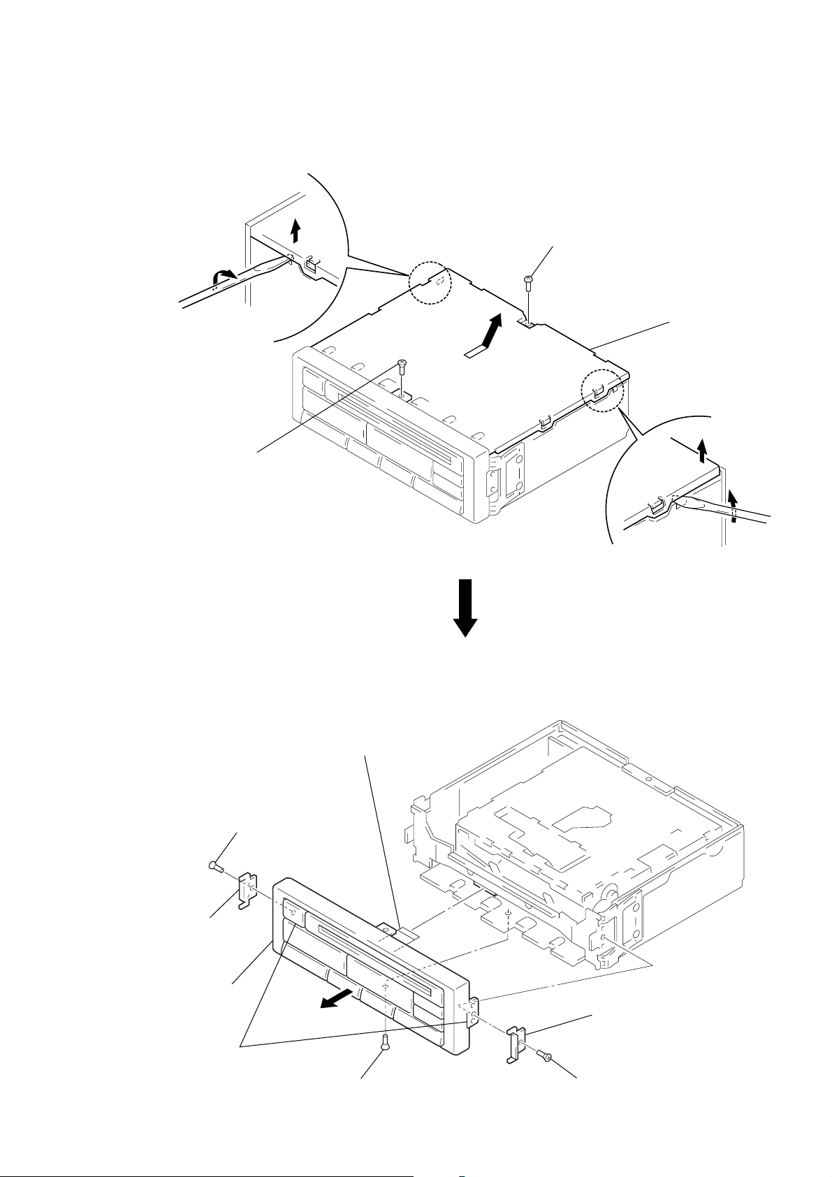
SECTION 1
DISASSEMBLY
Note: Follow the disassembly procedure in the numerical order given.
CASE
3
1
screw (K2.6 × 6)
4
5
1
screw (PTT2.6 × 5)
case
4
3
FRONT PANEL
3
reinforcement
4
2
front panel
two claws
screw (K2.6 × 6)
6
flat cable (CN104)
5
3
reinforcement
1
screw (K2.6 × 6)
2
screw (K2.6 × 6)
3
Page 4
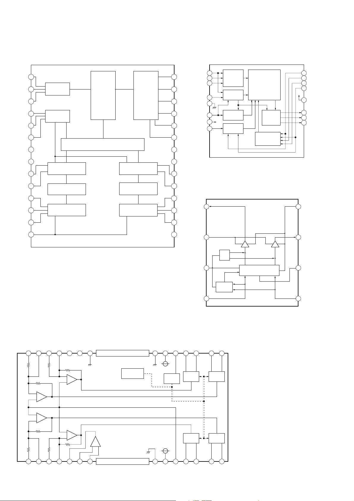
• IC Block Diagrams
IC301 PCM1710U-A/1K (MD MAIN BOARD)
1
LRCIN
DIN
BCKIN
CLKO
XTI
XTO
DGND
2
3
4
5
6
7
INPUT
INTERFACE DIGITAL
TIMING
CONTROL
FILTER
NOISE
SHAPER
SECTION 2
DIAGRAMS
28
MODE
CONTROL
27
26
25
24
23
22
IC302 SM5852CS-E2 (MD MAIN BOARD)
LRCI
ML/DSD
MC/DM2
MD/DM1
MUTE
MODE
CKSL
DGND
BCKI
CLK
VSS
RSTN
TESTN
MUTEN
1
2
3
DI
4
5
6
7
8
INPUT
INTERFACE
SYSTEM
CLOCK
SEQUENTIAL
CONTROL
MUTE
CONTROL
DIGITAL
SIGNAL
PROCESSOR
INTERFACE
CONTROL
OUTPUT
MODE
DB/DS
16
MOD2
15
MOD1
14
OPT
13
VDD
12
LRCO
11
BCKO
10
DOUT
9
V
VCC2R
GND2R
EXT1R
EXT2R
VOUTR
GND1
8
DD
9
10
11
12
13
14
5-LEVEL DAC
RIGHT
LOW-PASS FILTER
RIGHT
3-STAGE AMP
RIGHT
5-LEVEL DAC
LEFT
LOW-PASS FILTER
LEFT
3-STAGE AMP
LEFT
21
DD
V
20
VCC2L
19
GND2L
IC401 BA6287F (MD MAIN BOARD)
18
EXT1L
OUT1
VM
VCC
FIN
1
2
DRIVER DRIVER
TSD
3
POWER
SAVE
4
CONTROL LOGIC
EXT2L
17
16
VOUTL
VCC1
15
GND
8
OUT2
7
VREF
6
RIN
5
IC402 BA6394F (MD MAIN BOARD)
28 27 26 25 24 23 22 21 20 19 18 17 16 15
–
+
–
+
+
–
+
–
1 2 3 4 5 6 7 8 9 10 11 12 13 14
GND
OP-AMP
+
–
THERMAL
SHUTDOWN
GND VCC
GND VCC
DRIVER
MUTE
BIAS
DRIVER
CH3
DRIVER
CH2
4
– +– +
DRIVER
CH4
DRIVER
CH1
– +– +
Page 5
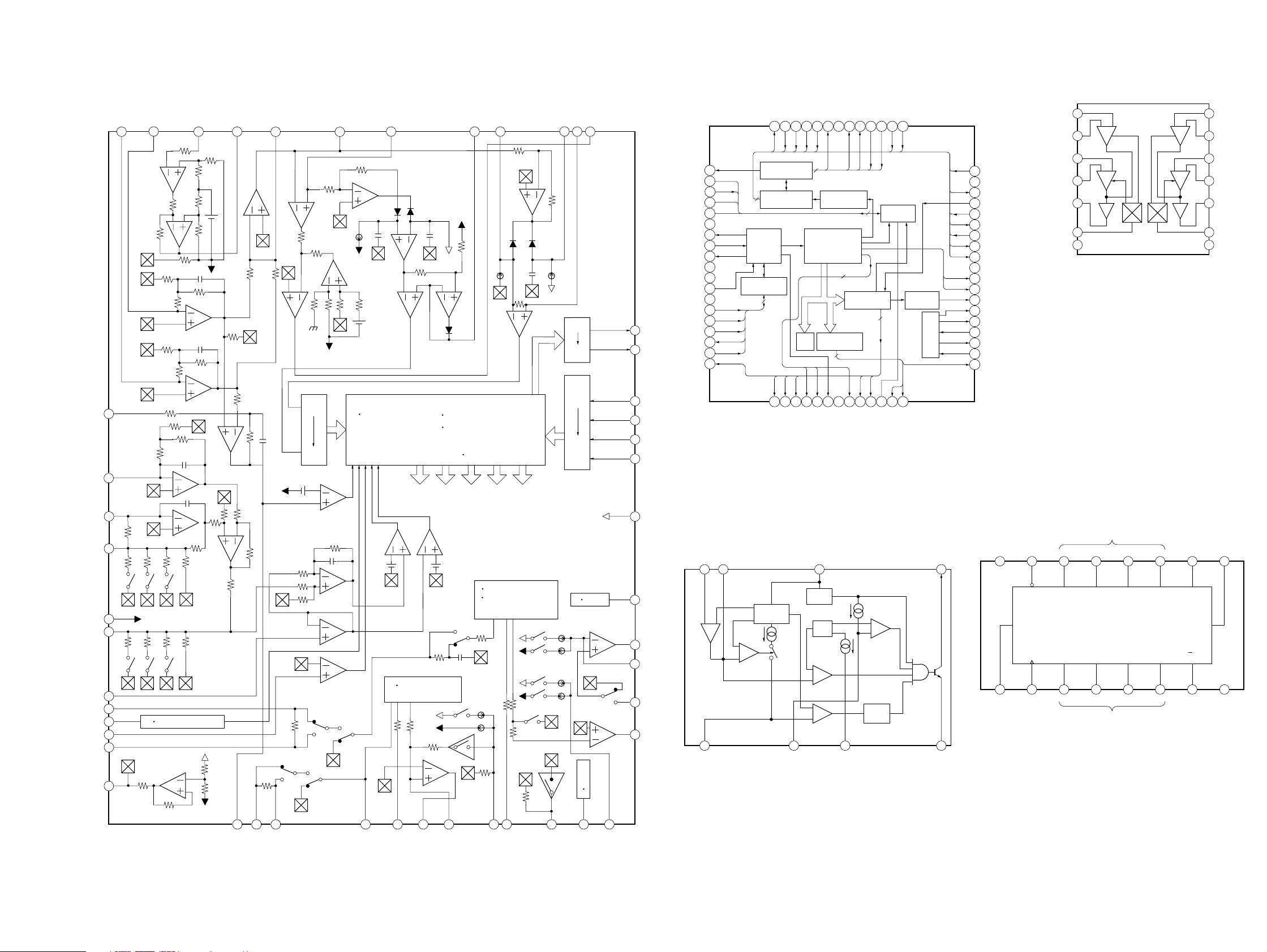
IC501 CXA1782BR (MD MAIN BOARD) IC502 CXD2507AQ (MD MAIN BOARD)
1
2
3
4
5
6
7
8
9
10
11
12
13
14
15
16
17
18
51
50
49
48
47
46
45
44
43
42
41
40
39
38
37
36
35
34
33
32313029282726252423222120
52535455565758596061626364
19
FOK
MON
MDP
MDS
LOCK
TEST
FILO
FILI
PCO
VSS
AVSS
CLTV
AVDD
RF
BIAS
ASYI
ASYO
ASYE
WDCK
DATA
XRST
SENS
MUTE
SQCK
SQSO
EXCK
SBSO
SCOR
V
SS
WFCK
EMPH
DOUT
C4M
FSTT
XTSL
XTAO
XTAI
MNTO
SERVO AUTO
SEQUENCER
CPU
INTERFACE
DIGITAL
CLV
SUB CODE
PROCESSOR
EFM
DEMODULATOR
DIGITAL
PLL
ASYMMETRY
CORRECTOR
D/A
INTERFACE
ERROR
CORRECTOR
16K
RAM
DIGITAL
OUT
CLOCK
GENERATOR
LRCK
BCLK
GTOP
XUGF
XPCK
V
DD
GFS
RFCK
CZPO
XROF
MNT3
MNT1
XLON
SPOD
SPOC
SPOB
SPOA
CLKO
V
DD
XLTO
DATO
CNIN
SEIN
CLOK
XLAT
3
5
14
4
5
3
6
PHD 2
PHD 1
36 35 34
PHD
LD
33
RF M
32
RF O
31
RF I
30 29 28 27 26 25
CP
CB
CC1
CC2
FOK
IC101 BA3129F-T1 (MAIN BOARD)
+IN2A
+IN1A
–IN1A
1
+
–
2
14
+
–
–IN2A
13
3
+IN1B
+
–
4
–IN1B
OUT1
5
SW1
6
DFCT
FDFCT
FOK
LEVEL S
MIRR
DFCT
TTL
IIL
FZC COMP
TZC COMP
DFCT
FS4
IIL DATA REGISTER
HPF COMP
TM1
43
FGD
TOG1-3
BAL1-3
FCS PHASE
COMPENSATION
5
6
FLB
INPUT SHIFT REGISTER
ADDRESS DECODER
OUTPUT DECODER
FS1-4 TG1-2 TM1-7 PS1-4
TG1
FS1
TRACKING
PHASE
COMPENSATION
SRCH
LPF COMP
FE O
FS2
FE M
TM6
TM5
TM4
TM3
TM7
TG2
987
TGU
IIL
TTL
TTL
IIL
ISET
F SET
11
10
TG2
FSET
TM2
24
SENS
C.OUT
23
XRST
22
21
DATA
20
XLT
19
CLK
VCC
18
ISET
17
SL O
16
SL M
15
SL P
14
13
TA O
12
TA M
IC401 TL5001CD (MAIN BOARD)
VCC
U.V.L.O
OSC
–
+
PWM
COMPARATOR
–
+
S.C.P.
COMPARATOR 2
6 7
CONTROL
DEAD-TIME
ERROR
AMP
INPUTSCP
+
–
5
FEED BACK
REFERENCE
VOLTAGE
+
–
S.C.P.
COMPARATOR 1
SWITCH
'ON'
AT
'H'
RT
DEAD-TIME
COMPARATOR
–
+
S.C.P.
LATCH
OUT
1234
8
GND
IC502 SN74HC165ANS (KEY BOARD)
CLOCK
INHIBIT
VCC
CLOCK
INHIBIT
SHIFT/
LOAD
CK
2 3
1
SHIFT/
CLOCK E F G H OUTPUT
LOAD
APC
RF IV AMP1
BAL2
TOG1
WINDOW COMP
RF IV AMP2
E IV AMP
BAL 3
TOG2
ATSC
TOG3
F IV AMP
TE AMP
FE AMP
1
FEO
2
FEI
FE BIAS
37
F
38
E
39
EI
40
BAL1
VEE
41
TED
42
LPFI
TEI
ATSC
TZC
TDFCT
43
44
45
46
47
48
VC
7
VEE
PARALLEL INPUTS
C B A SERIAL
D
EFGHQH
5 6 7 8
4
PARALLEL INPUTS
+
SERIAL
INPUTABCD
12
+IN2B
–
–IN2B
11
OUT2
10
SW2
9
8
VCC
OUTPUT
QH
91016 15 14 13 12 11
IN
QH
GND
QH
55
Page 6
XR3F-19B160
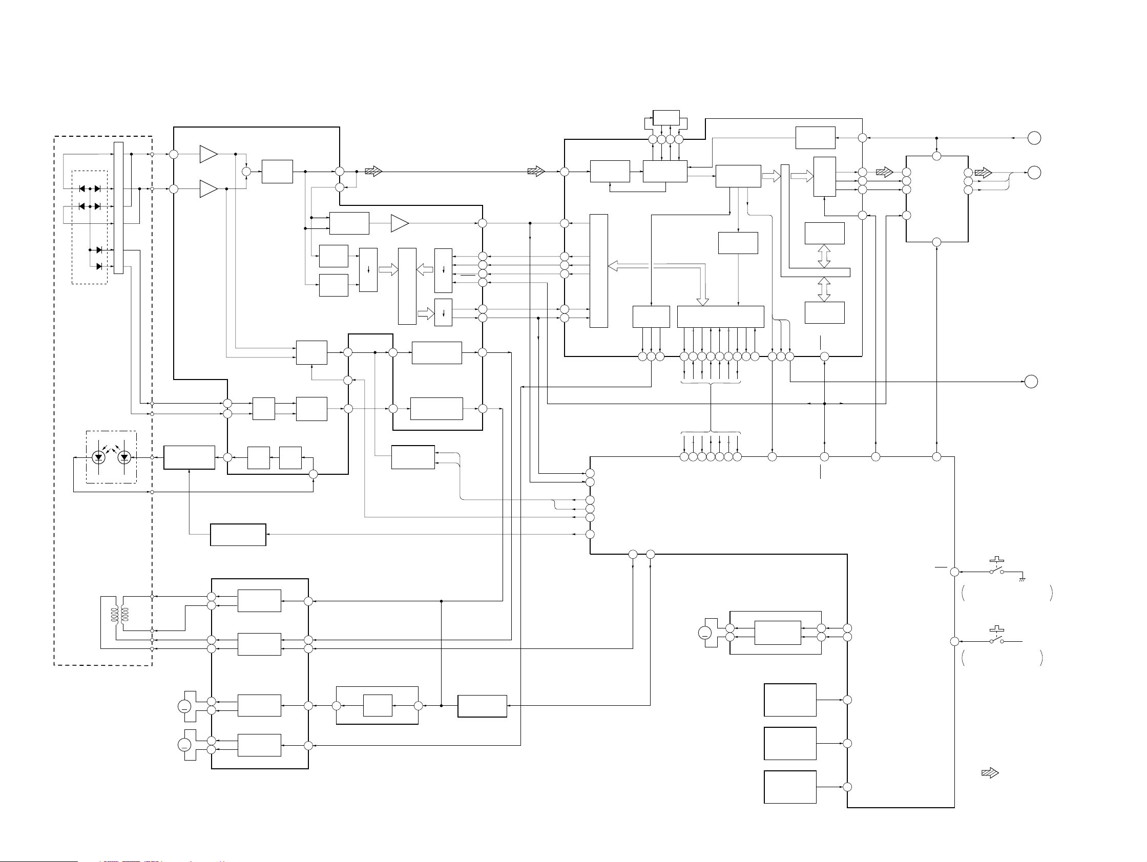
2-1. BLOCK DIAGRAM – SERVO Section –
DETECTOR
ABD
C
F
E
OPTICAL PICK-UP
(KSS-313B/Z-N)
LASER DIODE
I-V AMP
DIGITAL SIGNAL PROCESSOR,
CLV SERVO
IC502
RF AMP
PHD1
35
RF
+
RF AMP,
FOCUS/TRACKING
IC501 (1/2)
F
I-V
E
AMP
SUMMING
AMP
SERVO
RF AMP
PHD2
36
38
39
FOCUS
ERROR
AMP
TRACKING
ERROR
AMP
RFO
31
RFI
30
FOCUS OK
COMPARATOR
MIRR
AMP
DEFECT
AMP
FEO
FE BIAS
TEO
RF
FOK
DATO
CLKO
XLTO
SEIN
CNIN
ASYMMETRY
CORRECTION
SERVO AUTO SEQUENCER
14
FOK
DATA
XRST
SENS
C.OUT
CLK
XLT
FEO
TAO
25
21
19
20
22
24
23
6
13
FOCUS OK
AMP
TTL
IIL
1
37
42
FEI
2
TEI
44
TTL
IIL
IIL
IIL DATA REGISTER
TTL
FOCUS PHASE
COMPENSATION
TRACKING PHASE
COMPENSATION
1
56
59
57
54
55
7
FILO
DIGITAL PLL
DIGITAL
CLV
MON
MDP
FILTER
89
12
FILI
PCO
CLTV
CPU INTERFACE
MDS
SQSO
SQCK
SENS
46 47 49 51 53 52 43 44 45
DEMODULATOR
SUB-CODE
PROCESSOR
DATA
CLOK
XLAT
EFM
SCOR
SBSO
EXCK
27 41 40234
GFS
WFCK
CLOCK
GENERATOR
16K RAM
INTERNAL BUS
ERROR
CORRECTOR
EMPH
D/A
INTERFACE
XRST
50
XTAI
PCMD
BCK
LRCK
MUTE
34
4
21
22
20
48
CLK
3
DI
2
BCKI
1
LRCI
6
RSI
MD2
15
DOUT
BCKO
LRO
COMPRESSOR
IC302
C16M
DATA
9
BCK
10
LRCK
11
EMPH
A
(Page 7)
B
(Page 7)
C
(Page 7)
FG0
FG1
SLED ON SWITCH
Q504, 505
11 13 61 54 53 55 64
65
C.OUT
28
FOK
48
FG0
49
FG1
5
FO
29
APC
FGG
SLDON
4050
M903
(LOADING)
SQIN
SQCK
M
SENS
DCLK
DDATA
DLAT
1
7
OUT1
OUT2
27 52 22 24
SCOR
GFS
SYSTEM CONTROLLER
LOADING MOTOR DRIVE
IC401
LOADING
MOTOR DRIVE
DISC SIZE
(8cm/12cm)
DETECT SENSOR
D801, Q604
DISC IN
DETECT SENSOR
D802, Q605
IC601 (1/2)
RIN
XRST
FIN
4
5657LMOT1
5
1
2
LMOT2
PH1IN
PH2OR3
DMUTE
COMP
(DISC SET)
80DSW
ON : When completion of the disc
chucking operation.
79LSW
ON : When the optical pick-up
is inner position.
S601
S301
(LIMIT)
+5V
SLED
AMP
FOCUS GAIN
SWITCH
Q503
SLP
AUTOMATIC
POWER CONTROL
M902
M901
Q502
M
M
LD
PD
2-AXIS
DEVICE
(FOCUS)
(TRACKING)
05
(SLED)
(SPINDLE)
LD
LD
33
AMP
LASER ON SWITCH
Q501
FOCUS/TRACKING COIL DRIVE,
SPINDLE/SLED MOTOR DRIVE
IC402
VO2+
12
11
14
13
17
18
15
16
VO2–
VO1+
VO1–
VO3+
VO3–
VO4+
VO4–
TRACKING
COIL DRIVE
FOCUS
COIL DRIVE
SLED
MOTOR DRIVE
SPINDLE
MOTOR DRIVE
PD
AMP
VIN2
VIN1
VIN1’
VIN3
VIN4
PHD
34
3
1
2
26
28
SLO
16 14
SLED SERVO
IC501 (2/2)
• SIGNAL PATH
LOADING
COMPLETION
DETECT SENSOR
D804, Q607
PH4IN
3
: CD PLAY
66
Page 7
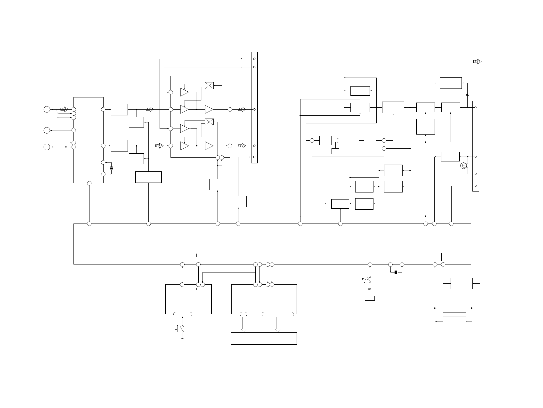
2-2. BLOCK DIAGRAM – MAIN Section –
XR3F-19B160
B
(Page 6)
A
(Page 6)
C
(Page 6)
C16M
EMPH
DIGITAL FILTER,
D/A CONVERTER
IC301
DATA LOUT
2
3
BCK
1
LRCK
4
CLKO
26
EMP1
27
EMP2
MUTE
3
AUDIO IN
R-CH
4
AUDIO IN
2
1
5
CN301
L-CH
AUDIO OUT
L-CH
AUDIO OUT
R-CH
CD LOGIC
SENSE
IN
4
D/A CONVERTER
(IC301) B+
+5V DRIVER,
ERROR
AMP
+5V ACC
SERVO
SYSTEM B+
IC402 B+
COMPARATOR
OSC
AUDIO CIRCUIT
(IC101, 102) B+
B+ SWITCH
Q301, 302
B+ SWITCH
B+ SWITCH
PWM
POWER CONTROL
+5V
Q602, 603
Q609, 610
IC401
+5V
REGULATOR
IC404
+5V
REGULATOR
IC402
OUTPUT
CIRCUIT
+10V (VFD)
VCC
OUT
SWITCHING
REGULATOR
Q406, 407
1
2
+10V
REGULATOR
Q405
RIPPLE
FILTER
Q408
BACK-UP
REGULATOR
Q409, 411
REGULATOR
CONTROL
SWITCH
Q410
+5V
REGULATOR
Q401
B+ SWITCH
Q403, 404
LEVEL SHIFT
D302
PL501 – 506
LINE AMP & SWITCH
IC101
IN2A
13
SW1
SW2
96
CD/EXIT
SWITCHING
Q302
OUT2
OUT1
10
5
CD LOGIC
SENSE
Q304
TO MASTER UNIT
LOW-PASS
FILTER
16
IC102 (1/2)
MUTING
Q101
LOW-PASS
FILTER
13
ROUT
XTI
XTO
25
IC102 (2/2)
MUTING
5
6
X301
16.93MHz
Q201
MUTING
CONTROL SWITCH
Q301
IN2B
11
IN1A
2
IN1B
4
• SIGNAL PATH
: CD PLAY
D401
4
BATT
3
LAMP+
1
LAMP–
5
RADIO ON
CN201
POWER
CONNECTOR
6
DAMUTE
05
21 25 26
AMUTE
QH
78 77
QH
A – H
11 – 14, 3 – 6 37 – 27, 25 – 19, 17 – 11
S502 – 509
SH/LO
19 2 44 432042 47
S/L
KEY CONTROL
IC502
CDON
CLK
LGSENS
VFCLK
VFDAT
18 17 16 15
1G, 2G
2, 3
FLUORESCENT INDICATOR TUBE
VFLAT
CLDICE
VFD501
VFINH
BLK
P1 – P25
FL DRIVER
IC501
SVP
SYSTEM CONTROLLER
IC601 (2/2)
14
DAON
S501
EJECT
EJKEY
X2
X601
4.19MHz
19 76 62
POWER
LAMPIN
X1
706966
BATTCHK
RADIOON
RESET
6063
RESET SIGNAL
SYSTEM RESET
IC403
BATTERY CHECK
Q402
GENERATOR
IC602
BACK-UP
BATT
77
Page 8
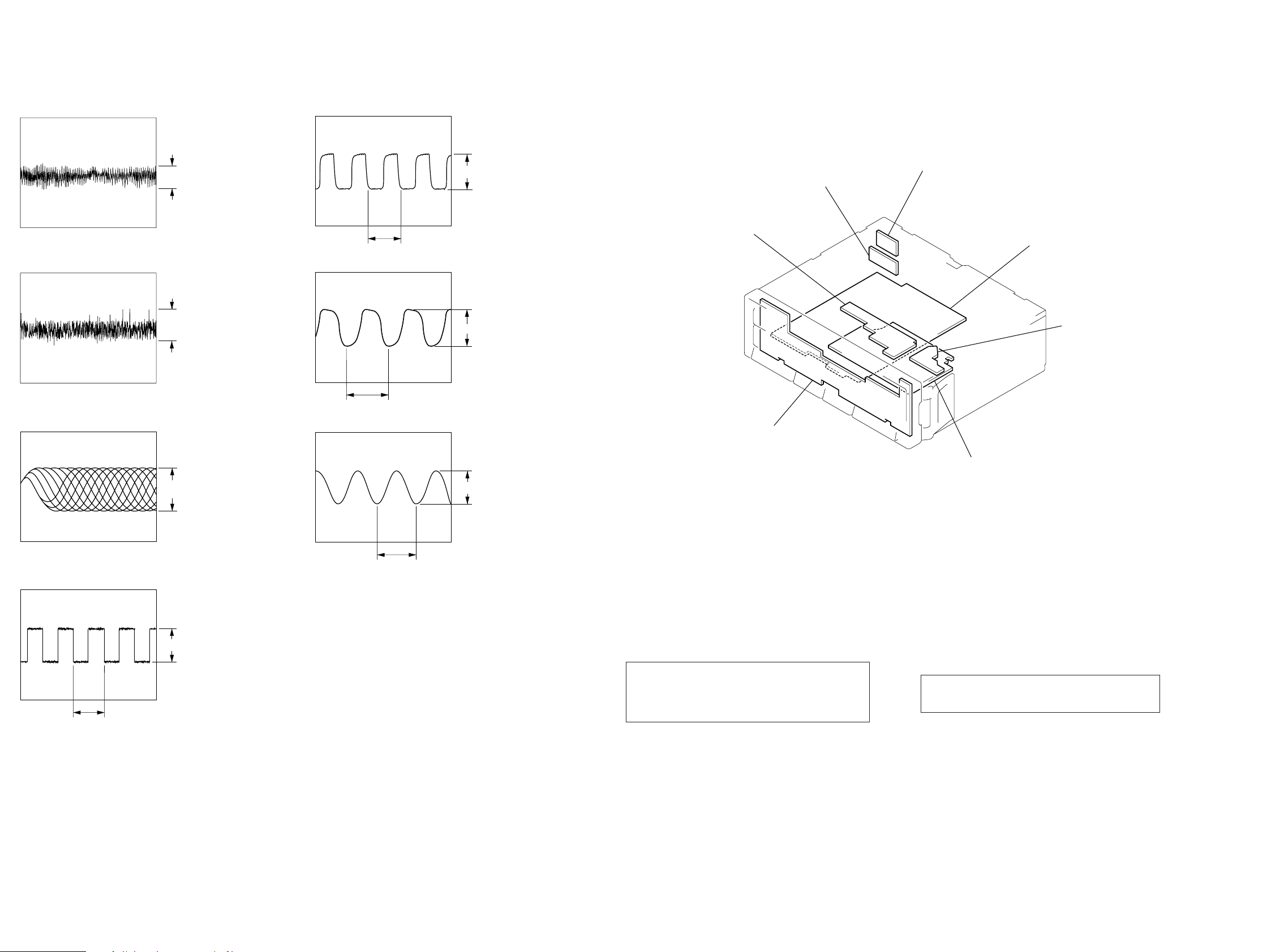
• Waveforms (MD MAIN BOARD)
• Circuit Boards Location
1 IC501 $™ (TEO)
2 IC501 1 (FEO)
3 IC501 #¡ (RF O)
Approx.
156 mVp-p
Approx.
132 mVp-p
5 IC502 @™ (BCK)
470 ns
6 IC601 ^ª (X2)
236 ns
7 IC301 5 (XTI)
5 Vp-p
5 Vp-p
POWER CONNECTOR board
SIGNAL CONNECTOR board
SENSOR board
MAIN board
MOTOR board
KEY board
4 IC502 @º (LRCK)
22 µs
Approx.
1.1 Vp-p
5 Vp-p
59 ns
3 Vp-p
MD MAIN board
2-3. NOTE FOR PRINTED WIRING BOARDS AND SCHEMATIC DIAGRAMS
Note on Printed Wiring Board:
• X : parts extracted from the component side.
• Y : parts extracted from the conductor side.
r
•
•
• b : Pattern from the side which enables seeing.
(The other layers' patterns are not indicated.)
Caution:
Pattern face side: Parts on the pattern face side seen from
(Side B) the pattern face are indicated.
Parts face side: Parts on the parts face side seen from
(Side A) the parts face are indicated.
: Through hole.
¢
: internal component.
Note on Schematic Diagram:
• All capacitors are in µF unless otherwise noted. pF: µµF
50 WV or less are not indicated except for electrolytics
and tantalums.
• All resistors are in Ω and 1/
specified.
¢
•
• C : panel designation.
Note: The components identified by mark ! or dotted line
• U : B+ Line.
• Power voltage is dc 14.4V and fed with regulated dc power
• Voltages and waveforms are dc with respect to ground
• Voltages are taken with a VOM (Input impedance 10 MΩ ).
• Waveforms are taken with a oscilloscope.
• Circled numbers refer to waveforms.
• Signal path.
: internal component.
with mark ! are critical for safety.
Replace only with part number specified.
supply from ACC and BATT cords.
under no-signal conditions.
no mark : CD PLAY
Voltage variations may be noted due to normal production tolerances.
Voltage variations may be noted due to normal production tolerances.
J : CD PLAY
: Impossible to measure
∗
4
W or less unless otherwise
88
Page 9

2-4. PRINTED WIRING BOARDS – SERVO Section –
XR3F-19B160
• Semiconductor Location
Ref. No. Location
D801 A-11
D802 B-7
D804 A-7
IC301 F-11
IC302 G-2
IC401 G-7
IC402 D-8
IC501 E-9
Ref. No. Location
IC502 G-10
IC601 F-8
IC602 G-4
Q301 E-2
Q302 F-2
Q501 E-4
Q502 E-3
Q503 E-8
(Page 12)
Ref. No. Location
Q504 F-9
Q505 F-9
Q602 G-1
Q603 G-1
Q604 F-1
Q605 G-5
Q607 F-5
Q609 F-4
Q610 F-4
99
Page 10

XR3F-19B160
2-5. SCHEMATIC DIAGRAM – SERVO Section (1/2) – • See page 8 for Waveforms. • See page 4 for IC Block Diagrams.
The components identified by mark ! or dotted
line with mark ! are critical for safety.
Replace only with part number specified.
1010
Page 11

2-6. SCHEMATIC DIAGRAM – SERVO Section (2/2) – • See page 8 for Waveforms. • See page 4 for IC Block Diagrams.
XR3F-19B160
(Page 13)
1111
Page 12

XR3F-19B160
2-7. PRINTED WIRING BOARDS – MAIN Section – • See page 8 for Circuit Boards Location.
(Page 9)
• Semiconductor Location
Ref. No. Location
D302 D-2
D303 E-3
D401 C-4
D402 C-4
D403 D-5
D404 F-3
D405 G-5
D406 C-5
D408 C-5
IC101 A-4
IC102 B-2
IC401 G-4
IC402 C-1
IC403 C-5
IC404 C-2
Ref. No. Location
Q101 B-3
Q201 B-3
Q301 C-3
Q302 B-4
Q304 D-3
Q401 D-5
Q402 D-5
Q403 F-4
Q404 F-3
Q405 F-3
Q406 G-5
Q407 G-5
Q408 D-1
Q409 F-4
Q410 G-4
Q411 G-4
(Page 14)
1212
Page 13

2-8. SCHEMATIC DIAGRAM – MAIN Section – • See page 5 for IC Block Diagrams.
(Page
11)
XR3F-19B160
(Page
14)
1313
Page 14

XR3F-19B160
2-9. PRINTED WIRING BOARD – KEY Board – • See page 8 for Circuit Boards Location. 2-10. SCHEMATIC DIAGRAM – KEY Board – • See page 5 for IC Block Diagram.
(Page 12)
(Page
13)
1414
Page 15

2-11. IC PIN FUNCTION DESCRIPTION
• MD MAIN BOARD IC601 µPD78052GC-123-3B9 (SYSTEM CONTROLLER)
1 PH1IN I
2 PH2OR3 I
3 PH4IN I
4 AVSS
5FOO
6 DAMUTE O
7 AVREF1
8 to 10 — —
11 SQIN I
12 — —
13 SQCK O
14 DAON O
15 VFINH O
16 VFLAT O
17 VFDAT O
18 VFCLK O
19 POWER O
20 SVP O
21 AMUTE O
22 DMUTE O
23 EECE O
24 COMP O
25 CDON O
26 LGSENS O
27 GFS I
28 FOK I
29 APC O
30 EECLK O
31 EESO O
32 EESI I
33 VSS
34 RDS I
35 to 39 — —
40 SLDON O
41 SEL0 I
42 SEL1 I
43 — —
44 to 47
O
48 FG0 O
49 FG1 O
Pin No. Pin Name I/O Description
ADJOK0 to
ADJOK3
Disc size (8 cm/12 cm) detect signal input from the photosensor (Q604)
“L”: 8 cm, “H”: 12 cm
Disc in detect signal input from the photosensor (Q605) “H”: disc is present
Disc loading completion detect signal input from the photosensor (Q607)
“H”: disc loading completed
— Ground terminal (for analog system)
Focusing offset automatic alignment signal output to the CXA1782BR (IC501)
Muting control signal output to the D/A converter (IC301) “L”: mute on
I Reference voltage input terminal (+5V) (for D/A converter)
Not used (open)
Subcode Q data input from the CXD2507AQ (IC502)
Not used (open)
Subcode Q data reading clock signal output to the CXD2507AQ (IC502)
D/A converter (IC301) power supply on/off control signal output terminal “H”: power on
Inhibit output to the fluorescent indicator tube driver (IC501) “L” active
Serial data latch pulse output to the fluorescent indicator tube driver (IC501)
Serial data output to the fluorescent indicator tube driver (IC501)
Serial data transfer clock signal output to the fluorescent indicator tube driver (IC501) and key
control (IC502)
Main system power supply on/off control signal output terminal “H”: power on
Servo system power supply on/off control signal output terminal “H”: power on
Audio mute on/off control signal output terminal “H”: mute on
Digital mute on/off control signal output to the CXD2507AQ (IC502) “H”: mute on
Not used (open)
Analog compression signal output to the SM5852CS (IC302)
CD/exit input signal select control signal output to the BA3129F (IC101)
“L”: exit input, “H”: CD on
CD logic sense signal output to the external master unit
Guard frame sync signal input from the CXD2507AQ (IC502) “L”: NG, “H”: OK
Focus OK signal input from the CXD2507AQ (IC502) “L”: NG, “H”: OK
Laser diode on/off control signal output terminal “L”: laser on
Not used (open)
Not used (open)
Not used (open)
— Ground terminal (for digital system)
Not used (open)
Not used (open)
Sledding servo on/off control signal output terminal
Mode selection input terminal (fixed at “L” in this set)
Mode selection input terminal (fixed at “L” in this set)
Not used (open)
Automatic alignment monitor output terminal
Not used (open)
Focusing gain automatic alignment signal output to the CXA1782BR (IC501)
Focusing gain automatic alignment signal output to the CXA1782BR (IC501)
15
Page 16

Pin No. Pin Name I/O Description
n
50 FGG O
51 — —
52 XRST O
53 DCLK O
54 DDATA O
55 DLAT O
56 LMOT1 O
57 LMOT2 O
58 — —
59 IGN I
60 RESET I
61 SENS I
62 RADIOON I
63 BATTCHK I
64 SCOR I
65 C.OUT I
66 EJKEY I
67
68 VDD
69 X2 O
70 X1 I
71 IC —
72 — O
73 — I
74 AVDD
75 AVREF0 I
76 LAMPIN I
77 SH/LO O
78 QH I
79 LSW I
80 DSW I
BATTDET
(INSW)
Focusing gain automatic alignment signal output to the focus coil driver (IC402)
Not used (open)
Reset signal output to the SM5852CS (IC302), CXA1782BR (IC501) and CXD2507AQ (IC502)
“L”: reset
Serial data transfer clock signal output to the CXD2507AQ (IC502)
Serial data output to the CXD2507AQ (IC502)
Serial data latch pulse signal output to the CXD2507AQ (IC502)
Loading motor (M903) drive signal output terminal *1
Loading motor (M903) drive signal output terminal *1
Not used (open)
Ignition input terminal (connected to power supply in this set)
System reset signal input from the reset signal generator (IC602) “L”: reset
For several hundreds msec. after the power supply rises, “L” is input, then it changes to “H”
Internal status input from the CXD2507AQ (IC502)
Radio on/off control signal input from the power connector (CN201)
Backup power detection signal input terminal (used also to reset standby)
Subcode sync (S0+S1) detection signal input from the CXD2507AQ (IC502)
Track number count signal input from the CXA1782BR (IC501)
Inputs the disc eject switch (S501) detection signal
“L” is input while the switch is pressed (used also to reset standby)
—
Not used (open)
— Power supply terminal (+5V) (for digital system)
Main system clock output terminal (4.19 MHz)
Main system clock input terminal (4.19 MHz)
Internal connection terminal (normally connected to ground)
Not used (open)
Not used (fixed at “L”)
— Power supply terminal (+5V) (for analog system)
Reference voltage input terminal (+5V) (for A/D converter)
Lamp drive voltage input from the power connector (CN201)
Shift/load control signal output to the key control (IC502)
Key data input from the key control (IC502)
Inputs the sled limit in detect switch (S301) detection signal
“H”: When the optical pick-up is inner position
Inputs the disc set detect switch (S601) detection signal
“L”: When completion of the disc chucking operation
*1 Loading motor (M903) control
Operatio
Terminal
LMOT1 (pin %§)
LMOT2 (pin %¶)
OFF OUT IN BRAKE
“H” “L” “H” “L”
“H” “H” “L” “L”
16
Page 17

SECTION 3
d
EXPLODED VIEWS
NOTE:
• -XX and -X mean standardized parts, so they
may have some difference from the original
one.
• Color Indication of Appearance Parts
Example:
KNOB, BALANCE (WHITE) . . . (RED)
↑↑
Parts Color Cabinet's Color
(1) GENERAL
4
• Items marked “*” are not stocked since they
are seldom required for routine service. Some
delay should be anticipated when ordering
these items.
• The mechanical parts with no reference number in the exploded views are not supplied.
• Hardware (# mark) list and accessories and
packing materials are given in the last of the
electrical parts list.
MG-205F-132
#3
5
The components identified by
mark ! or dotted line with mark
! are critical for safety.
Replace only with part number
specified.
6
#3
#3
#3
CN301
10
key board unit
2
10
1
not supplied
10
10
1
Ref. No. Part No. Description Remark
* 1 3-362-079-01 REINFORCEMENT (PANEL)
2 3-342-659-01 SCREW (SPRING CLIP)
* 3 1-654-932-11 SIGNAL CONNECTOR BOARD
* 4 3-917-782-01 CASE
5 1-775-347-11 CABLE, FLEXIBLE FLAT (25 CORE)
9
CN201
3
#2
7
#2
8
#3
not supplie
2
Ref. No. Part No. Description Remark
* 7 A-3309-933-A MAIN BOARD, COMPLETE
* 8 3-917-806-04 CHASSIS
* 9 1-654-931-11 POWER CONNECTOR BOARD
10 2-641-430-01 SCREW (2.6X6), (+) K TAPPING
CN201 1-569-522-11 PIN, CONNECTOR 6P
* 6 3-917-783-01 BRACKET
CN301 1-565-094-11 SOCKET, CONNECTOR 6P
17
Page 18

(2) KEY BOARD UNIT
51
58
52
69
75
53
54
62
60
55
70
65
57
56
62
67
63
59
VFD501
68
63
61
PL504-507
76
#10
73
#10
71
#10
PL501-503
68
66
Ref. No. Part No. Description Remark
* 51 A-3291-761-A PANEL ASSY
52 3-913-332-11 BUTTON, SEESAW (= AMS +)
53 3-913-333-11 BUTTON (SCAN)
54 3-913-333-01 BUTTON ((p PLAY/STOP)
55 3-913-332-01 BUTTON, SEESAW (0 REV/FF ))
56 3-913-331-01 BUTTON, SHUFFLE
57 3-913-330-01 BUTTON, COMPRESS
58 3-913-329-01 BUTTON, EJECT
59 3-913-319-01 PANEL, FRONT
* 60 3-913-325-01 GUIDE (EJ), LIGHT
* 61 3-913-322-01 GUIDE (A), LIGHT
* 62 3-913-323-01 GUIDE (B), LIGHT
* 63 3-913-324-01 GUIDE (C), LIGHT
* 65 3-913-327-01 PLATE, SHIELD
66 X-3377-305-1 PANEL ASSY, SUB
* 67 A-3294-090-A KEY BOARD, COMPLETE
18
Ref. No. Part No. Description Remark
68 3-913-335-02 SPACER
69 3-913-328-02 COVER, DISPLAY
70 3-917-138-01 SPACER
* 71 3-917-809-01 SHEET, INSULATING
73 X-3377-304-1 DISPLAY ASSY
75 3-936-377-01 TAPE (FILTER)
76 3-917-810-01 SPACER (FL TUBE)
PL501 1-517-554-11 LAMP, PILOT (BLUE)
PL502 1-517-554-11 LAMP, PILOT (BLUE)
PL503 1-517-554-11 LAMP, PILOT (BLUE)
PL504 1-517-554-11 LAMP, PILOT (BLUE)
PL505 1-517-554-11 LAMP, PILOT (BLUE)
PL506 1-517-554-11 LAMP, PILOT (BLUE)
PL507 1-517-554-11 LAMP, PILOT (BLUE)
VFD501 1-517-360-11 INDICATOR TUBE, FLUORESCENT
Page 19

(3) MECHANISM DECK SECTION-1
(MG-205F-132)
110
103
112
113
140
125
115
103
112
114
126
124
110
109
108
107
106
102
137
120
105
116
105
#5
#4
A
121
118
119
117
127
141
101
122
#5
128
#5
129
130
M903
138
A
132
#5
133
134
135
136
Ref. No. Part No. Description Remark
* 101 A-3309-934-A MD MAIN BOARD, COMPLETE
102 3-384-894-01 GEAR (R1
103 3-384-900-01 SPRING (PRESS)
105 3-578-242-11 WASHER
* 106 3-029-143-01 GEAR (R2/F)
107 3-384-896-01 GEAR (DOWN)
108 X-3366-858-4 ARM ASSY, FRICTION
109 3-384-899-01 SPRING (FRICTION)
110 3-384-892-01 BEARING (ROLLER)
112 3-701-438-11 WASHER, 2.5
113 3-909-408-01 ROLLER (T)
114 3-386-150-01 RING (ROLLER), RETAINING
115 A-3252-591-A GEAR ASSY, ROLLER
* 116 X-3373-302-2 CHASSIS (M) ASSY
117 3-384-923-01 SHAFT (DAMPER)
118 3-384-916-01 SPRING (FL)
119 3-384-914-01 DAMPER
* 120 3-384-915-11 BRACKET (CP)
* 121 3-384-918-21 RETAINER (DISC)
Ref. No. Part No. Description Remark
122 3-384-908-31 ARM, CHUCKING
124 3-384-888-01 SLIDER (L)
125 3-384-887-01 LEVER (L)
* 126 3-906-923-03 GUIDE (DISK 2)
* 127 1-653-378-13 SENSOR BOARD
* 128 X-3377-273-1 CHASSIS (TB) ASSY
129 3-384-881-02 SPRING (12)
130 3-384-917-01 SPRING (CH)
132 X-3366-102-1 SLIDER (R) ASSY
* 133 X-3366-853-1 CHASSIS (R) ASSY
134 3-384-889-01 LEVER (R)
135 3-384-897-01 GEAR (RACK)
136 3-384-891-11 LEVER (ST)
137 3-388-331-11 SPRING (T)
138 3-387-776-01 BELT (L)
* 140 X-3366-857-1 ARM ASSY, ROLLER
141 3-918-103-01 SCREW (TOOTH) (+P 2)
M903 A-3252-580-A MOTOR (L) ASSY (LOADING)
19
Page 20

(4) MECHANISM DECK SECTION-2
(MG-205F-132)
157
163
M901
#9
154
M902
153
156
155
162
152
158
#5
159
#6
160
151
161
#7
Ref. No. Part No. Description Remark
151 A-3252-586-A SHAFT (SL) ASSY
! 152 8-848-407-11 OPTICAL PICK-UP (KSS-313B/Z-RP)
153 3-384-922-01 GEAR (SL FEED)
154 3-384-920-11 RETAINER (SL FEED)
* 155 1-653-379-13 MOTOR BOARD
156 1-653-376-11 MOTOR FLEXIBLE BOARD
* 157 X-3370-190-1 CHASSIS (OPT) ASSY (OUTSERT)
158 X-3366-100-1 BASE (DRIVING) ASSY
20
Ref. No. Part No. Description Remark
159 3-384-912-11 GEAR (K2)
160 3-570-615-02 POLY-WASHER (DIA.1.2)
161 3-384-913-11 SPRING (THRUST RETAINER)
162 3-918-103-11 SCREW (TOOTH) (+P 2)
163 3-926-152-01 SCREW (+P 1.7X2.5)
M901 X-3376-192-1 SPINDLE MOTOR ASSY
M902 A-3252-585-A MOTOR (SL) ASSY (SLED)
The components identified by mark ! or dotted
line with mark ! are critical for safety.
Replace only with part number specified.
Page 21

SECTION 4
ELECTRICAL PARTS LIST
KEY MAIN
NOTE:
• Due to standardization, replacements in the
parts list may be different from the parts specified in the diagrams or the components used
on the set.
• -XX and -X mean standardized parts, so they
may have some difference from the original
one.
• RESISTORS
All resistors are in ohms.
METAL: Metal-film resistor.
METAL OXIDE: Metal oxide-film resistor.
F: nonflammable
Ref. No. Part No. Description Remark Ref. No. Part No. Description Remark
* A-3294-090-A KEY BOARD, COMPLETE
********************
3-913-335-02 SPACER
3-917-810-01 SPACER (FL TUBE)
< CAPACITOR >
C501 1-164-346-11 CERAMIC CHIP 1uF 16V
C502 1-164-346-11 CERAMIC CHIP 1uF 16V
C503 1-163-243-11 CERAMIC CHIP 47PF 5% 50V
C504 1-164-346-11 CERAMIC CHIP 1uF 16V
< IC >
• Items marked “*” are not stocked since they
are seldom required for routine service.
Some delay should be anticipated when ordering these items.
• SEMICONDUCTORS
In each case, u: µ, for example:
uA. . : µA. . uPA. . : µPA. .
uPB. . : µPB. . uPC. . : µPC. .
uPD. . : µPD. .
• CAPACITORS
uF: µF
• COILS
uH: µH
PL503 1-517-554-11 LAMP, PILOT (BLUE)
PL504 1-517-554-11 LAMP, PILOT (BLUE)
PL505 1-517-554-11 LAMP, PILOT (BLUE)
PL506 1-517-554-11 LAMP, PILOT (BLUE)
PL507 1-517-554-11 LAMP, PILOT (BLUE)
R501 1-216-226-00 RES, CHIP 15K 5% 1/8W
R502 1-216-206-00 RES, CHIP 2.2K 5% 1/8W
R503 1-216-206-00 RES, CHIP 2.2K 5% 1/8W
R504 1-216-206-00 RES, CHIP 2.2K 5% 1/8W
R505 1-216-206-00 RES, CHIP 2.2K 5% 1/8W
The components identified by
mark ! or dotted line with mark
! are critical for safety.
Replace only with part number
specified.
When indicating parts by reference
number, please include the board.
< RESISTOR >
IC501 8-759-823-73 IC LC7574E
IC502 8-759-926-25 IC SN74HC165ANS
< SHORT >
JC501 1-216-296-00 SHORT 0
JC502 1-216-296-00 SHORT 0
JC503 1-216-296-00 SHORT 0
JC504 1-216-296-00 SHORT 0
JC505 1-216-296-00 SHORT 0
JC506 1-216-296-00 SHORT 0
JC507 1-216-296-00 SHORT 0
JC508 1-216-296-00 SHORT 0
JC509 1-216-296-00 SHORT 0
JC510 1-216-296-00 SHORT 0
JC511 1-216-296-00 SHORT 0
JC512 1-216-296-00 SHORT 0
JC513 1-216-296-00 SHORT 0
JC514 1-216-296-00 SHORT 0
JC515 1-216-296-00 SHORT 0
JC516 1-216-296-00 SHORT 0
JC517 1-216-296-00 SHORT 0
JC518 1-216-296-00 SHORT 0
JC519 1-216-296-00 SHORT 0
JC520 1-216-296-00 SHORT 0
R506 1-216-206-00 RES, CHIP 2.2K 5% 1/8W
R507 1-216-206-00 RES, CHIP 2.2K 5% 1/8W
R508 1-216-206-00 RES, CHIP 2.2K 5% 1/8W
R509 1-216-206-00 RES, CHIP 2.2K 5% 1/8W
R510 1-215-864-00 METAL OXIDE 150 5% 1W F
< SWITCH >
S501 1-553-479-00 SWITCH, PUSH (EJECT)
S502 1-553-479-00 SWITCH, PUSH (=)
S503 1-553-479-00 SWITCH, PUSH (+)
S504 1-553-479-00 SWITCH, PUSH (SCAN)
S505 1-553-479-00 SWITCH, PUSH (”p PLAY/STOP)
S506 1-553-479-00 SWITCH, PUSH (0)
S507 1-553-479-00 SWITCH, PUSH ())
S508 1-553-479-00 SWITCH, PUSH (SHUFFLE)
S509 1-553-479-00 SWITCH, PUSH (COMPRESS)
< FLUORESCENT INDICATOR TUBE >
VFD501 1-517-360-11 INDICATOR TUBE, FLUORESCENT
**************************************************************
* A-3309-933-A MAIN BOARD, COMPLETE
*********************
< CAPACITOR >
JC521 1-216-296-00 SHORT 0
JC522 1-216-296-00 SHORT 0
JC523 1-216-296-00 SHORT 0
< PILOT LAMP >
PL501 1-517-554-11 LAMP, PILOT (BLUE)
PL502 1-517-554-11 LAMP, PILOT (BLUE)
C101 1-163-093-00 CERAMIC CHIP 10PF 5% 50V
C102 1-163-093-00 CERAMIC CHIP 10PF 5% 50V
C103 1-124-967-11 ELECT 10uF 20% 10V
C104 1-124-967-11 ELECT 10uF 20% 10V
C105 1-163-011-11 CERAMIC CHIP 0.0015uF 10% 50V
C106 1-124-233-11 ELECT 10uF 20% 16V
C110 1-164-695-11 CERAMIC CHIP 0.0022uF 5% 50V
21
Page 22

MAIN
Ref. No. Part No. Description Remark
C111 1-163-124-00 CERAMIC CHIP 200PF 5% 50V
C112 1-135-149-21 TANTALUM CHIP 2.2uF 20% 10V
C113 1-163-138-00 CERAMIC CHIP 750PF 5% 50V
C201 1-163-093-00 CERAMIC CHIP 10PF 5% 50V
C202 1-163-093-00 CERAMIC CHIP 10PF 5% 50V
C203 1-107-714-11 ELECT 10uF 20% 16V
C204 1-107-714-11 ELECT 10uF 20% 16V
C205 1-163-011-11 CERAMIC CHIP 0.0015uF 10% 50V
C206 1-124-233-11 ELECT 10uF 20% 16V
C210 1-164-695-11 CERAMIC CHIP 0.0022uF 5% 50V
C211 1-163-124-00 CERAMIC CHIP 200PF 5% 50V
C212 1-135-149-21 TANTALUM CHIP 2.2uF 20% 10V
C213 1-163-138-00 CERAMIC CHIP 750PF 5% 50V
C301 1-163-021-11 CERAMIC CHIP 0.01uF 10% 50V
C302 1-163-021-11 CERAMIC CHIP 0.01uF 10% 50V
C303 1-164-004-11 CERAMIC CHIP 0.1uF 10% 25V
C305 1-163-109-00 CERAMIC CHIP 47PF 5% 50V
C306 1-124-233-11 ELECT 10uF 20% 16V
C308 1-163-038-00 CERAMIC CHIP 0.1uF 25V
C401 1-163-809-11 CERAMIC CHIP 0.047uF 10% 25V
C402 1-107-710-11 ELECT 100uF 20% 25V
C403 1-164-004-11 CERAMIC CHIP 0.1uF 10% 25V
C404 1-125-701-11 DOUBLE LAYER 0.047F 5.5V
C405 1-104-665-11 ELECT 100uF 20% 10V
C406 1-124-589-11 ELECT 47uF 20% 16V
C407 1-124-589-11 ELECT 47uF 20% 16V
C408 1-126-316-51 ELECT 470uF 20% 16V
C409 1-126-163-11 ELECT 4.7uF 20% 50V
C410 1-164-004-11 CERAMIC CHIP 0.1uF 10% 25V
C412 1-126-247-11 ELECT 560uF 20% 6.3V
C413 1-164-004-11 CERAMIC CHIP 0.1uF 10% 25V
C414 1-126-916-11 ELECT 1000uF 20% 6.3V
C415 1-124-233-11 ELECT 10uF 20% 16V
C416 1-164-004-11 CERAMIC CHIP 0.1uF 10% 25V
C417 1-124-584-00 ELECT 100uF 20% 10V
C418 1-163-038-00 CERAMIC CHIP 0.1uF 25V
C419 1-163-021-11 CERAMIC CHIP 0.01uF 10% 50V
C420 1-163-038-00 CERAMIC CHIP 0.1uF 25V
C421 1-163-009-11 CERAMIC CHIP 0.001uF 10% 50V
C422 1-124-584-00 ELECT 100uF 20% 10V
C423 1-128-057-11 ELECT 330uF 20% 6.3V
C424 1-164-346-11 CERAMIC CHIP 1uF 16V
C425 1-163-038-00 CERAMIC CHIP 0.1uF 25V
C426 1-163-038-00 CERAMIC CHIP 0.1uF 25V
C427 1-164-004-11 CERAMIC CHIP 0.1uF 10% 25V
< CONNECTOR >
Ref. No. Part No. Description Remark
D404 8-719-110-21 DIODE RD11ES-B1
D405 8-719-938-78 DIODE SB10-05PCP
D406 8-719-109-88 DIODE RD5.6ES-B1
D408 8-719-109-86 DIODE RD5.1ES-B3
< IC >
IC101 8-759-326-81 IC BA3129F-T1
IC102 8-759-385-17 IC NJM4580E (TE2)
IC401 8-759-521-35 IC TL5001CD
IC402 8-759-150-61 IC uPC78L05T
IC403 8-759-326-78 IC PST9140NL
IC404 8-759-150-61 IC uPC78L05T
< COIL >
* L401 1-411-380-11 INDUCTOR 3.5mH
L402 1-411-161-11 INDUCTOR 47uH
L403 1-411-287-31 INDUCTOR 1mH
< TRANSISTOR >
Q101 8-729-920-31 TRANSISTOR DTC343TK
Q201 8-729-920-31 TRANSISTOR DTC343TK
Q301 8-729-011-47 TRANSISTOR XN4311
Q302 8-729-421-22 TRANSISTOR UN2211
Q304 8-729-011-47 TRANSISTOR XN4311
Q401 8-729-106-68 TRANSISTOR 2SD1615A-GP
Q402 8-729-424-73 TRANSISTOR UN2219
Q403 8-729-820-61 TRANSISTOR 2SB1124-T
Q404 8-729-421-22 TRANSISTOR UN2211
Q405 8-729-120-28 TRANSISTOR 2SC1623-L5L6
Q406 8-729-820-61 TRANSISTOR 2SB1124-T
Q407 8-729-402-84 TRANSISTOR XN4601
Q408 8-729-807-52 TRANSISTOR 2SD1623-T
Q409 8-729-808-69 TRANSISTOR 2SB1204T-FA
Q410 8-729-120-28 TRANSISTOR 2SC1623-L5L6
Q411 8-729-120-28 TRANSISTOR 2SC1623-L5L6
< RESISTOR >
R103 1-216-089-00 RES, CHIP 47K 5% 1/10W
R104 1-216-697-11 METAL CHIP 82K 0.5% 1/10W
R105 1-216-089-00 RES, CHIP 47K 5% 1/10W
R106 1-216-089-00 RES, CHIP 47K 5% 1/10W
R107 1-216-009-00 RES, CHIP 22 5% 1/10W
R110 1-216-073-00 METAL CHIP 10K 5% 1/10W
R111 1-216-073-00 METAL CHIP 10K 5% 1/10W
R112 1-216-073-00 METAL CHIP 10K 5% 1/10W
R113 1-216-073-00 METAL CHIP 10K 5% 1/10W
R114 1-216-073-00 METAL CHIP 10K 5% 1/10W
* CN101 1-506-988-11 PIN, CONNECTOR (PC BOARD) 6P
* CN102 1-506-989-11 PIN, CONNECTOR (PC BOARD) 7P
CN103 1-770-073-11 CONNECTOR, FFC/FPC (ZIF) 25P
CN104 1-770-074-11 CONNECTOR, FFC/FPC (ZIF) 16P
< DIODE >
D302 8-719-110-35 DIODE RD13ES-B1
D303 8-719-989-93 DIODE SB01-15CP-TB
D401 8-719-200-82 DIODE 11ES2
D402 8-719-109-90 DIODE RD5.6ESB3
D403 8-719-110-48 DIODE RD18ES-B1
22
R115 1-216-097-00 RES, CHIP 100K 5% 1/10W
R203 1-216-089-00 RES, CHIP 47K 5% 1/10W
R204 1-216-697-11 METAL CHIP 82K 0.5% 1/10W
R205 1-216-089-00 RES, CHIP 47K 5% 1/10W
R206 1-216-089-00 RES, CHIP 47K 5% 1/10W
R207 1-216-009-00 RES, CHIP 22 5% 1/10W
R210 1-216-073-00 METAL CHIP 10K 5% 1/10W
R211 1-216-073-00 METAL CHIP 10K 5% 1/10W
R212 1-216-073-00 METAL CHIP 10K 5% 1/10W
R213 1-216-073-00 METAL CHIP 10K 5% 1/10W
Page 23

MAIN MD MAIN
Ref. No. Part No. Description Remark
R214 1-216-073-00 METAL CHIP 10K 5% 1/10W
R215 1-216-097-00 RES, CHIP 100K 5% 1/10W
R301 1-216-121-00 RES, CHIP 1M 5% 1/10W
R303 1-216-033-00 METAL CHIP 220 5% 1/10W
R306 1-216-057-00 METAL CHIP 2.2K 5% 1/10W
R307 1-216-073-00 METAL CHIP 10K 5% 1/10W
R308 1-216-097-00 RES, CHIP 100K 5% 1/10W
R309 1-216-093-11 RES, CHIP 68K 5% 1/10W
R310 1-216-089-00 RES, CHIP 47K 5% 1/10W
R311 1-216-009-00 RES, CHIP 22 5% 1/10W
R312 1-216-073-00 METAL CHIP 10K 5% 1/10W
R313 1-216-422-11 METAL OXIDE 18 5% 1W F
R315 1-216-049-11 RES, CHIP 1K 5% 1/10W
R316 1-216-049-11 RES, CHIP 1K 5% 1/10W
R317 1-216-049-11 RES, CHIP 1K 5% 1/10W
R318 1-216-049-11 RES, CHIP 1K 5% 1/10W
R320 1-216-049-11 RES, CHIP 1K 5% 1/10W
R321 1-216-049-11 RES, CHIP 1K 5% 1/10W
R323 1-216-089-00 RES, CHIP 47K 5% 1/10W
R324 1-216-089-00 RES, CHIP 47K 5% 1/10W
R401 1-216-081-00 METAL CHIP 22K 5% 1/10W
R403 1-216-105-00 RES, CHIP 220K 5% 1/10W
R404 1-249-419-11 CARBON 1.5K 5% 1/4W
R405 1-249-419-11 CARBON 1.5K 5% 1/4W
R406 1-216-079-00 METAL CHIP 18K 5% 1/10W
Ref. No. Part No. Description Remark
C302 1-107-826-11 CERAMIC CHIP 0.1uF 10% 16V
C303 1-135-166-21 TANTALUM CHIP 47uF 10% 10V
C304 1-109-982-11 CERAMIC CHIP 1uF 10% 10V
C305 1-162-923-11 CERAMIC CHIP 47PF 5% 50V
C306 1-109-982-11 CERAMIC CHIP 1uF 10% 10V
C307 1-162-923-11 CERAMIC CHIP 47PF 5% 50V
C401 1-126-206-11 ELECT CHIP 100uF 20% 6.3V
C402 1-107-826-11 CERAMIC CHIP 0.1uF 10% 16V
C403 1-164-005-11 CERAMIC CHIP 0.47uF 25V
C404 1-164-357-11 CERAMIC CHIP 1000PF 5% 50V
C405 1-164-156-11 CERAMIC CHIP 0.1uF 25V
C406 1-164-156-11 CERAMIC CHIP 0.1uF 25V
C407 1-126-206-11 ELECT CHIP 100uF 20% 6.3V
C501 1-164-677-11 CERAMIC CHIP 0.033uF 10% 16V
C502 1-162-970-11 CERAMIC CHIP 0.01uF 10% 25V
C503 1-164-677-11 CERAMIC CHIP 0.033uF 10% 16V
C504 1-162-970-11 CERAMIC CHIP 0.01uF 10% 25V
C505 1-126-206-11 ELECT CHIP 100uF 20% 6.3V
C507 1-162-970-11 CERAMIC CHIP 0.01uF 10% 25V
C508 1-162-970-11 CERAMIC CHIP 0.01uF 10% 25V
C509 1-163-809-11 CERAMIC CHIP 0.047uF 10% 25V
C510 1-164-471-11 CERAMIC CHIP 680PF 5% 50V
C511 1-164-227-11 CERAMIC CHIP 0.022uF 10% 25V
C512 1-164-004-11 CERAMIC CHIP 0.1uF 10% 25V
C513 1-164-357-11 CERAMIC CHIP 1000PF 5% 50V
R407 1-216-097-00 RES, CHIP 100K 5% 1/10W
R408 1-216-095-00 METAL CHIP 82K 5% 1/10W
R409 1-216-041-00 METAL CHIP 470 5% 1/10W
R410 1-216-059-00 METAL CHIP 2.7K 5% 1/10W
R411 1-216-089-00 RES, CHIP 47K 5% 1/10W
R412 1-216-033-00 METAL CHIP 220 5% 1/10W
R413 1-216-682-11 METAL CHIP 20K 0.5% 1/10W
R414 1-216-667-11 METAL CHIP 4.7K 0.5% 1/10W
R415 1-216-093-11 RES, CHIP 68K 5% 1/10W
R416 1-216-093-11 RES, CHIP 68K 5% 1/10W
R417 1-216-097-00 RES, CHIP 100K 5% 1/10W
R418 1-216-037-00 METAL CHIP 330 5% 1/10W
R419 1-216-065-00 RES, CHIP 4.7K 5% 1/10W
R420 1-216-065-00 RES, CHIP 4.7K 5% 1/10W
R421 1-216-069-00 METAL CHIP 6.8K 5% 1/10W
R422 1-216-089-00 RES, CHIP 47K 5% 1/10W
R424 1-216-057-00 METAL CHIP 2.2K 5% 1/10W
R425 1-216-073-00 METAL CHIP 10K 5% 1/10W
R426 1-216-073-00 METAL CHIP 10K 5% 1/10W
< VARISTOR >
VDR401 1-807-601-11 VARISTOR, CERAMIC
**************************************************************
* A-3309-934-A MD MAIN BOARD, COMPLETE
************************
< CAPACITOR >
C101 1-164-676-11 CERAMIC CHIP 2200PF 5% 16V
C102 1-135-259-11 TANTALUM CHIP 10uF 20% 6.3V
C201 1-164-676-11 CERAMIC CHIP 2200PF 5% 16V
C202 1-135-259-11 TANTALUM CHIP 10uF 20% 6.3V
C301 1-162-919-11 CERAMIC CHIP 22PF 5% 50V
C514 1-164-005-11 CERAMIC CHIP 0.47uF 25V
C515 1-164-004-11 CERAMIC CHIP 0.1uF 10% 25V
C516 1-164-004-11 CERAMIC CHIP 0.1uF 10% 25V
C517 1-126-603-11 ELECT CHIP 4.7uF 20% 35V
C518 1-164-004-11 CERAMIC CHIP 0.1uF 10% 25V
C519 1-162-970-11 CERAMIC CHIP 0.01uF 10% 25V
C520 1-164-004-11 CERAMIC CHIP 0.1uF 10% 25V
C521 1-135-259-11 TANTALUM CHIP 10uF 20% 6.3V
C522 1-163-809-11 CERAMIC CHIP 0.047uF 10% 25V
C523 1-162-965-11 CERAMIC CHIP 0.0015uF 10% 50V
C524 1-162-927-11 CERAMIC CHIP 100PF 5% 50V
C525 1-164-004-11 CERAMIC CHIP 0.1uF 10% 25V
C526 1-162-970-11 CERAMIC CHIP 0.01uF 10% 25V
C527 1-164-173-11 CERAMIC CHIP 0.0039uF 10% 50V
C528 1-162-919-11 CERAMIC CHIP 22PF 5% 50V
C529 1-164-677-11 CERAMIC CHIP 0.033uF 10% 16V
C530 1-135-259-11 TANTALUM CHIP 10uF 20% 6.3V
C531 1-162-921-11 CERAMIC CHIP 33PF 5% 50V
C601 1-135-166-21 TANTALUM CHIP 47uF 10% 10V
C603 1-109-982-11 CERAMIC CHIP 1uF 10% 10V
C604 1-124-778-00 ELECT CHIP 22uF 20% 6.3V
C605 1-107-826-11 CERAMIC CHIP 0.1uF 10% 16V
C606 1-126-206-11 ELECT CHIP 100uF 20% 6.3V
C607 1-162-970-11 CERAMIC CHIP 0.01uF 10% 25V
C608 1-126-206-11 ELECT CHIP 100uF 20% 6.3V
C609 1-126-206-11 ELECT CHIP 100uF 20% 6.3V
C610 1-107-826-11 CERAMIC CHIP 0.1uF 10% 16V
C611 1-107-826-11 CERAMIC CHIP 0.1uF 10% 16V
C614 1-107-826-11 CERAMIC CHIP 0.1uF 10% 16V
C615 1-107-826-11 CERAMIC CHIP 0.1uF 10% 16V
C616 1-162-927-11 CERAMIC CHIP 100PF 5% 50V
C617 1-135-216-11 TANTALUM CHIP 10uF 20% 10V
C618 1-164-004-11 CERAMIC CHIP 0.1uF 10% 25V
23
Page 24

MD MAIN
Ref. No. Part No. Description Remark
C619 1-164-004-11 CERAMIC CHIP 0.1uF 10% 25V
< CONNECTOR >
CN601 1-750-992-21 CONNECTOR, FPC 25P
CN602 1-766-491-11 CONNECTOR, FPC 17P
* CN603 1-580-055-21 PIN, CONNECTOR (SMD) 2P
CN604 1-770-345-21 CONNECTOR, FPC 7P
* CN605 1-580-055-21 PIN, CONNECTOR (SMD) 2P
< IC >
IC301 8-759-569-27 IC PCM1710U-A/1K
IC302 8-759-326-80 IC SM5852CS-E2
IC401 8-759-040-83 IC BA6287F
IC402 8-759-188-68 IC BA6394FP
IC501 8-752-068-53 IC CXA1782BR
IC502 8-752-372-94 IC CXD2507AQ
IC601 8-759-457-83 IC uPD78052GC-123-3B9
IC602 8-759-326-78 IC PST9140NL
< COIL >
L301 1-412-058-11 INDUCTOR CHIP 10uH
L501 1-412-058-11 INDUCTOR CHIP 10uH
L601 1-412-058-11 INDUCTOR CHIP 10uH
L603 1-412-058-11 INDUCTOR CHIP 10uH
L605 1-412-058-11 INDUCTOR CHIP 10uH
< TRANSISTOR >
Q301 8-729-029-06 TRANSISTOR DTC124EUA-T106
Q302 8-729-141-48 TRANSISTOR 2SB624-BV345
Q501 8-729-141-48 TRANSISTOR 2SB624-BV345
Q502 8-729-141-48 TRANSISTOR 2SB624-BV345
Q503 8-729-929-64 TRANSISTOR UMG4-TL
Q504 8-729-905-57 TRANSISTOR DTA124EU
Q505 8-729-029-06 TRANSISTOR DTC124EUA-T106
Q602 8-729-141-48 TRANSISTOR 2SB624-BV345
Q603 8-729-029-06 TRANSISTOR DTC124EUA-T106
Q604 8-729-032-35 PHOTO TRANISTOR CPT-230S-C-TU
(8/12 DETECT)
Ref. No. Part No. Description Remark
R506 1-216-001-00 METAL CHIP 10 5% 1/10W
R507 1-216-832-11 METAL CHIP 8.2K 5% 1/16W
R509 1-216-833-11 RES, CHIP 10K 5% 1/16W
R510 1-216-845-11 METAL CHIP 100K 5% 1/16W
R511 1-216-847-11 METAL CHIP 150K 5% 1/16W
R512 1-216-853-11 METAL CHIP 470K 5% 1/16W
R513 1-216-848-11 METAL CHIP 180K 5% 1/16W
R515 1-216-839-11 METAL CHIP 33K 5% 1/16W
R516 1-216-839-11 METAL CHIP 33K 5% 1/16W
R517 1-216-836-11 METAL CHIP 18K 5% 1/16W
R518 1-216-855-11 METAL CHIP 680K 5% 1/16W
R519 1-216-845-11 METAL CHIP 100K 5% 1/16W
R520 1-218-273-11 RES, CHIP 510K 5% 1/16W
R521 1-216-845-11 METAL CHIP 100K 5% 1/16W
R522 1-216-829-11 METAL CHIP 4.7K 5% 1/16W
R523 1-216-851-11 METAL CHIP 330K 5% 1/16W
R524 1-216-845-11 METAL CHIP 100K 5% 1/16W
R525 1-216-843-11 METAL CHIP 68K 5% 1/16W
R526 1-216-849-11 METAL CHIP 220K 5% 1/16W
R530 1-216-827-11 METAL CHIP 3.3K 5% 1/16W
R531 1-216-827-11 METAL CHIP 3.3K 5% 1/16W
R532 1-216-833-11 RES, CHIP 10K 5% 1/16W
R533 1-216-856-11 METAL CHIP 820K 5% 1/16W
R534 1-216-849-11 METAL CHIP 220K 5% 1/16W
R535 1-216-833-11 RES, CHIP 10K 5% 1/16W
R536 1-216-833-11 RES, CHIP 10K 5% 1/16W
R537 1-216-837-11 METAL CHIP 22K 5% 1/16W
R538 1-216-836-11 METAL CHIP 18K 5% 1/16W
R539 1-216-841-11 METAL CHIP 47K 5% 1/16W
R540 1-216-841-11 METAL CHIP 47K 5% 1/16W
R541 1-216-836-11 METAL CHIP 18K 5% 1/16W
R542 1-216-834-11 METAL CHIP 12K 5% 1/16W
R543 1-216-837-11 METAL CHIP 22K 5% 1/16W
R602 1-216-841-11 METAL CHIP 47K 5% 1/16W
R603 1-216-841-11 METAL CHIP 47K 5% 1/16W
R604 1-216-849-11 METAL CHIP 220K 5% 1/16W
R605 1-216-845-11 METAL CHIP 100K 5% 1/16W
Q605 8-729-032-35 PHOTO TRANISTOR CPT-230S-C-TU
(DISC IN DETECT)
Q607 8-729-032-35 PHOTO TRANISTOR CPT-230S-C-TU
(LOADING COMPLETION)
Q609 8-729-807-35 TRANSISTOR 2SB1123-T
Q610 8-729-029-06 TRANSISTOR DTC124EUA-T106
< RESISTOR >
R301 1-216-821-11 METAL CHIP 1K 5% 1/16W
R302 1-216-809-11 METAL CHIP 100 5% 1/16W
R311 1-216-797-11 METAL CHIP 10 5% 1/16W
R312 1-216-809-11 METAL CHIP 100 5% 1/16W
R313 1-216-809-11 METAL CHIP 100 5% 1/16W
R401 1-216-839-11 METAL CHIP 33K 5% 1/16W
R402 1-216-849-11 METAL CHIP 220K 5% 1/16W
R403 1-216-849-11 METAL CHIP 220K 5% 1/16W
R501 1-216-797-11 METAL CHIP 10 5% 1/16W
R502 1-216-845-11 METAL CHIP 100K 5% 1/16W
R503 1-216-845-11 METAL CHIP 100K 5% 1/16W
R504 1-216-841-11 METAL CHIP 47K 5% 1/16W
R505 1-216-841-11 METAL CHIP 47K 5% 1/16W
24
R606 1-216-849-11 METAL CHIP 220K 5% 1/16W
R607 1-216-849-11 METAL CHIP 220K 5% 1/16W
R608 1-216-825-11 METAL CHIP 2.2K 5% 1/16W
R609 1-216-809-11 METAL CHIP 100 5% 1/16W
R610 1-216-825-11 METAL CHIP 2.2K 5% 1/16W
R611 1-216-825-11 METAL CHIP 2.2K 5% 1/16W
R612 1-216-825-11 METAL CHIP 2.2K 5% 1/16W
R613 1-216-825-11 METAL CHIP 2.2K 5% 1/16W
R614 1-216-825-11 METAL CHIP 2.2K 5% 1/16W
R615 1-216-809-11 METAL CHIP 100 5% 1/16W
R616 1-216-809-11 METAL CHIP 100 5% 1/16W
R617 1-216-809-11 METAL CHIP 100 5% 1/16W
R618 1-216-809-11 METAL CHIP 100 5% 1/16W
R619 1-216-825-11 METAL CHIP 2.2K 5% 1/16W
R620 1-216-809-11 METAL CHIP 100 5% 1/16W
R621 1-216-809-11 METAL CHIP 100 5% 1/16W
R622 1-216-809-11 METAL CHIP 100 5% 1/16W
R623 1-216-809-11 METAL CHIP 100 5% 1/16W
R624 1-216-037-00 METAL CHIP 330 5% 1/10W
R629 1-216-825-11 METAL CHIP 2.2K 5% 1/16W
Page 25

MD MAIN MOTOR POWER CONNECTOR SENSOR
SIGNAL CONNECTOR
Ref. No. Part No. Description Remark
R630 1-216-825-11 METAL CHIP 2.2K 5% 1/16W
R631 1-216-825-11 METAL CHIP 2.2K 5% 1/16W
R640 1-216-821-11 METAL CHIP 1K 5% 1/16W
R641 1-216-829-11 METAL CHIP 4.7K 5% 1/16W
R642 1-216-821-11 METAL CHIP 1K 5% 1/16W
R643 1-216-809-11 METAL CHIP 100 5% 1/16W
R650 1-216-841-11 METAL CHIP 47K 5% 1/16W
R651 1-216-841-11 METAL CHIP 47K 5% 1/16W
R660 1-216-833-11 RES, CHIP 10K 5% 1/16W
< SWITCH >
S601 1-571-754-31 SWITCH, PUSH (1 KEY) (DISC SET)
< VIBRATOR >
X301 1-760-401-11 VIBRATOR, CERAMIC (16.93MHz)
X601 1-579-063-21 VIBRATOR, CERAMIC (4.19MHz)
**************************************************************
* 1-653-379-13 MOTOR BOARD
*************
< CONNECTOR >
CNJ303 1-770-348-21 CONNECTOR, FPC 7P
< SWITCH >
S301 1-571-754-31 SWITCH, PUSH (1 KEY) (LIMIT)
**************************************************************
* 1-654-931-11 POWER CONNECTOR BOARD
************************
Ref. No. Part No. Description Remark
* 1-654-932-11 SIGNAL CONNECTOR BOARD
************************
< CONNECTOR >
CN301 1-565-094-11 SOCKET, CONNECTOR 6P
* CN302 1-506-988-11 PIN, CONNECTOR (PC BOARD) 6P
**************************************************************
MISCELLANEOUS
***************
5 1-775-347-11 CABLE, FLEXIBLE FLAT (25 CORE)
! 152 8-848-407-11 OPTICAL PICK-UP (KSS-313B/Z-RP)
156 1-653-376-11 MOTOR FLEXIBLE BOARD
M901 X-3376-192-1 SPINDLE MOTOR ASSY
M902 A-3252-585-A MOTOR (SL) ASSY (SLED)
M903 A-3252-580-A MOTOR (L) ASSY (LOADING)
************************************************************
**************
HARDWARE LIST
**************
#2 7-685-133-19 SCREW +P 2.6X6 TYPE2
#3 7-685-791-09 SCREW +PTT 2.6X5 (S)
#4 7-627-553-18 SCREW, PRECISION +P 2X2
#5 7-627-553-37 SCREW, PRECISION +P 2X3
#6 7-627-553-67 SCREW, PRECISION +P 2X5
#7 7-621-772-60 SCREW +B 2X12
#9 7-627-852-17 SCREW +P 1.7X4
#10 7-685-103-19 SCREW +P 2X5 TYPE2 NON-SLIT
< CAPACITOR >
C450 1-163-038-00 CERAMIC CHIP 0.1uF 25V
C451 1-163-038-00 CERAMIC CHIP 0.1uF 25V
C452 1-163-038-00 CERAMIC CHIP 0.1uF 25V
C453 1-163-038-00 CERAMIC CHIP 0.1uF 25V
< CONNECTOR >
CN201 1-569-522-11 PIN, CONNECTOR 6P
* CN202 1-506-989-11 PIN, CONNECTOR (PC BOARD) 7P
**************************************************************
* 1-653-378-13 SENSOR BOARD
D801 8-719-045-75 LED CL-200IR-X-TU (8/12 DETECT)
D802 8-719-045-75 LED CL-200IR-X-TU (DISC IN DETECT)
D804 8-719-045-75 LED CL-200IR-X-TU
R801 1-216-049-11 RES, CHIP 1K 5% 1/10W
R802 1-216-049-11 RES, CHIP 1K 5% 1/10W
R804 1-216-049-11 RES, CHIP 1K 5% 1/10W
**************************************************************
*************
< DIODE >
(LOADING COMPLETION)
< RESISTOR >
The components identified by mark ! or dotted
line with mark ! are critical for safety.
Replace only with part number specified.
25
Page 26

XR3F-19B160
9-926-580-11
26
Sony Corporation
Mobile Electronics Company
Printed in Japan © 1999. 6
99F05019-1
Published by Quality Assurance Dept.
 Loading...