

Page 1
XR-3100R
SERVICE MANUAL
SUPPLEMENT-1
File this supplement with the service manual.
Subject:
1. Sub Panel Modification
2. TEL ATT Cord Addition (XR-C33R ONLY)
/
(ECN-CSA02568, ENG-00013)
C33R
AEP Model
UK Model
TABLE OF CONTENTS
1. SUB PANEL MODIFICATION..................................... 2
2. TEL ATT CORD ADDITION
(XR-C33R (GREEN ILLUMINATION TYPE) ONLY)
2-1. Discrimination........................................................................ 3
2-2. Note for Printed Wiring Boards and
Schematic Diagrams .............................................................. 3
2-3. Printed Wiring Board
– MAIN Board (Component Side) – ..................................... 4
2-4. Printed Wiring Board
– MAIN Board (Conductor Side) – ....................................... 5
2-5. Schematic Diagram – MAIN Board (1/3) – .......................... 6
2-6. Schematic Diagram – MAIN Board (2/3) – .......................... 7
2-7. Schematic Diagram – MAIN Board (3/3) – .......................... 8
2-8. Exploded views ...................................................................... 9
2-9. Electrical Parts List ................................................................ 10
Page 2

1. SUB PANEL MODIFICATION
For the XR-3100R/C33R, the shape of sub panel has been changed in the midway of production.
Replace the sub panel with a new type, if the replacement becomes necessary.
Page Former type New type
Ref. No. Part No. Description Remark
35
1 3-030-828-01 PANEL, SUB
Ref. No. Part No. Description Remark
1 3-030-828-
02 PANEL, SUB
2
Page 3
2. TEL ATT CORD ADDITION (XR-C33R (GREEN ILLUMINATION TYPE) ONLY)
For the XR-C33R Spanish Model (green illumination type), the TEL ATT cord has been added in the midway of production.
This Service Manual Supplement-1 lists only the revised printed wiring board and schematic diagram of the XR-C33R.
For other information, refer to the Service Manual issued previously.
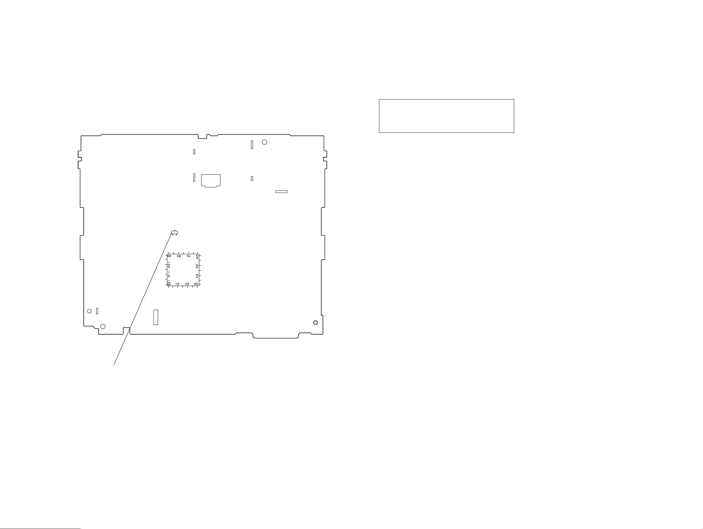
2-1. DISCRIMINATION
– MAIN Board (Component Side) –
Q571
IC501
2-2. NOTE FOR PRINTED WIRING BOARDS AND SCHEMATIC DIAGRAMS
Note on Printed Wiring Board:
• X : parts extracted from the component side.
• Y : parts extracted from the conductor side.
• b : Pattern from the side which enables seeing.
(The other layers' patterns are not indicated.)
Caution:
Pattern face side: Parts on the pattern face side seen from
(Conductor Side) the pattern face are indicated.
Parts face side: Parts on the parts face side seen from
(Component Side) the parts face are indicated.
Note on Schematic Diagram:
• All capacitors are in µF unless otherwise noted. pF: µµF
50 WV or less are not indicated except for electrolytics
and tantalums.
• All resistors are in Ω and 1/
specified.
f
•
• C : panel designation.
• U : B+ Line.
• H : adjustment for repair.
• Power v oltage is dc 14.4V and fed with regulated dc pow er
• Voltages and waveforms are dc with respect to ground
• V oltages are taken with a V OM (Input impedance 10 MΩ).
• Waveforms are taken with a oscilloscope.
• Circled numbers refer to waveforms.
• Signal path.
• Abbreviation
: internal component.
supply from ACC and BATT cords.
under no-signal (detuned) conditions.
no mark : FM
( ) : MW(LW)
〈〈 〉〉 : T APE PLA YBA CK
Voltage var iations may be noted due to normal production tolerances.
Voltage var iations may be noted due to normal production tolerances.
F : FM
f : MW(LW)
L : BUS AUDIO IN
E : TAPE PLAYBACK
AMBER : Amber illumination type
GREEN : Green illumination type
: Impossible to measure
∗
4
W or less unless otherwise
Q571 Mount : SPANISH MODEL (GREEN ILLUMINATION TYPE)
Q571 No Mount : EXCEPT SPANISH MODEL (GREEN ILLUMINATION TYPE)
33
Page 4
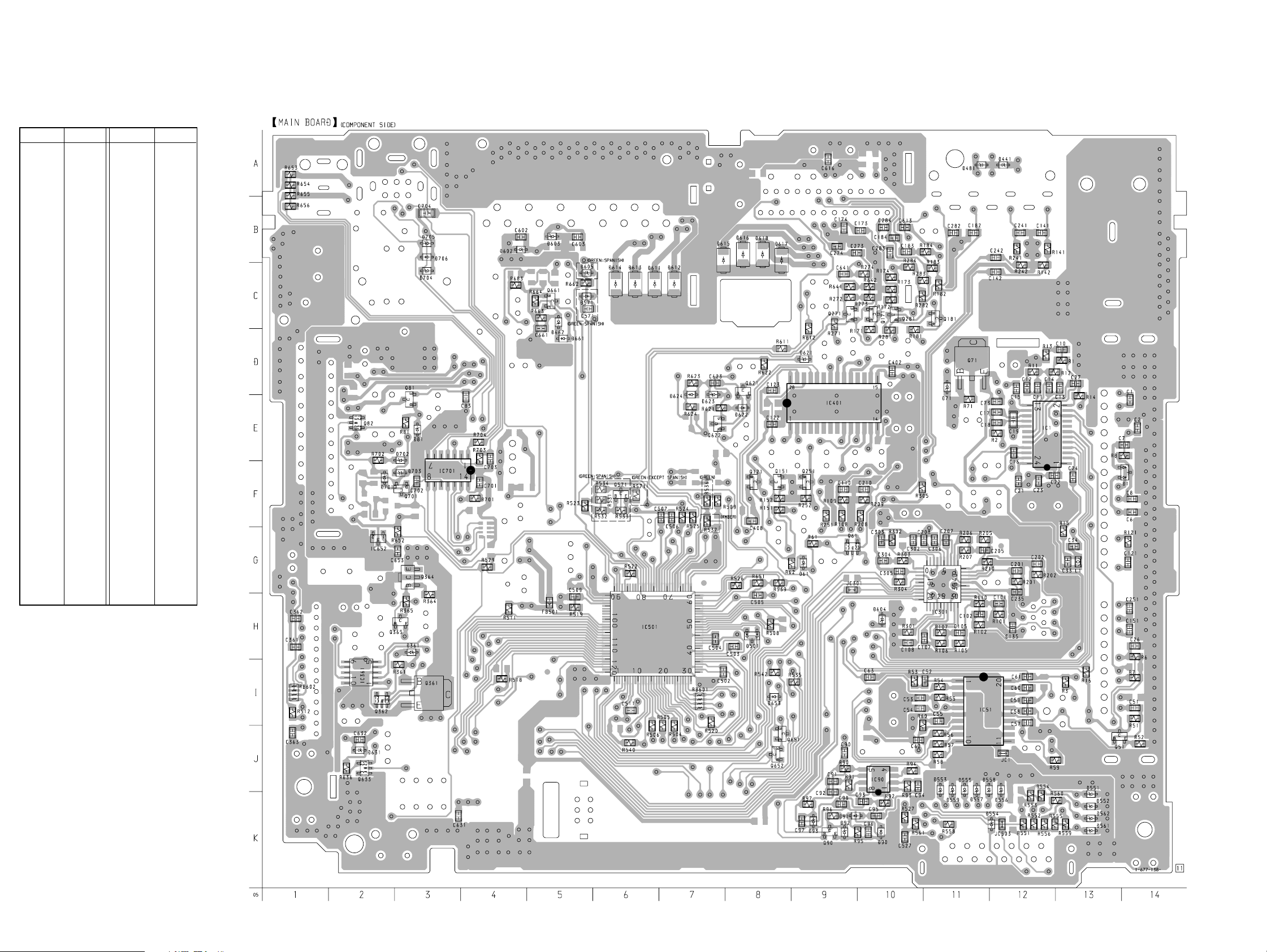
XR-3100R/C33R
2-3. PRINTED WIRING BOARD – MAIN Board (Component Side) –
• Semiconductor Location
Ref. No. Location
D1 F-14
D61 G-9
D71 D-11
D81 E-3
D90 K-10
D91 K-9
D92 K-9
D93 K-9
D361 H-3
D441 A-12
D481 A-11
D501 H-8
D551 K-13
D552 K-13
D553 J-11
D554 K-12
D555 J-11
D556 J-12
D557 J-11
D558 J-11
D559 J-11
D561 K-13
D562 K-13
D571 C-5
D602 B-4
D603 B-5
D604 H-10
D605 C-5
D611 C-6
D612 C-7
D613 C-6
D614 C-6
D615 B-7
D616 B-8
D617 B-8
D618 B-8
D621 D-9
D622 E-8
D623 E-7
D624 E-7
D631 J-2
D653 I-8
D661 D-5
D662 C-5
D701 F-2
Ref. No. Location
D702 E-3
D703 F-3
D704 C-3
D705 B-3
D706 B-3
D707 F-2
IC1 E-12
IC51 I-11
IC90 J-10
IC301 G-11
IC361 I-2
IC401 E-9
IC501 H-6
IC652 G-2
IC701 F-3
Q51 J-13
Q61 G-9
Q71 D-11
Q81 E-3
Q82 E-2
Q90 K-9
Q121 F-8
Q151 F-8
Q171 C-10
Q181 C-11
Q251 F-9
Q271 C-9
Q281 C-10
Q361 I-3
Q362 I-2
Q364 G-3
Q365 H-3
Q571 F-6
Q621 D-8
Q622 E-7
Q633 J-2
Q651 J-8
Q652 J-8
Q661 C-5
Q701 F-3
Q702 F-2
Q703 F-2
44
Page 5
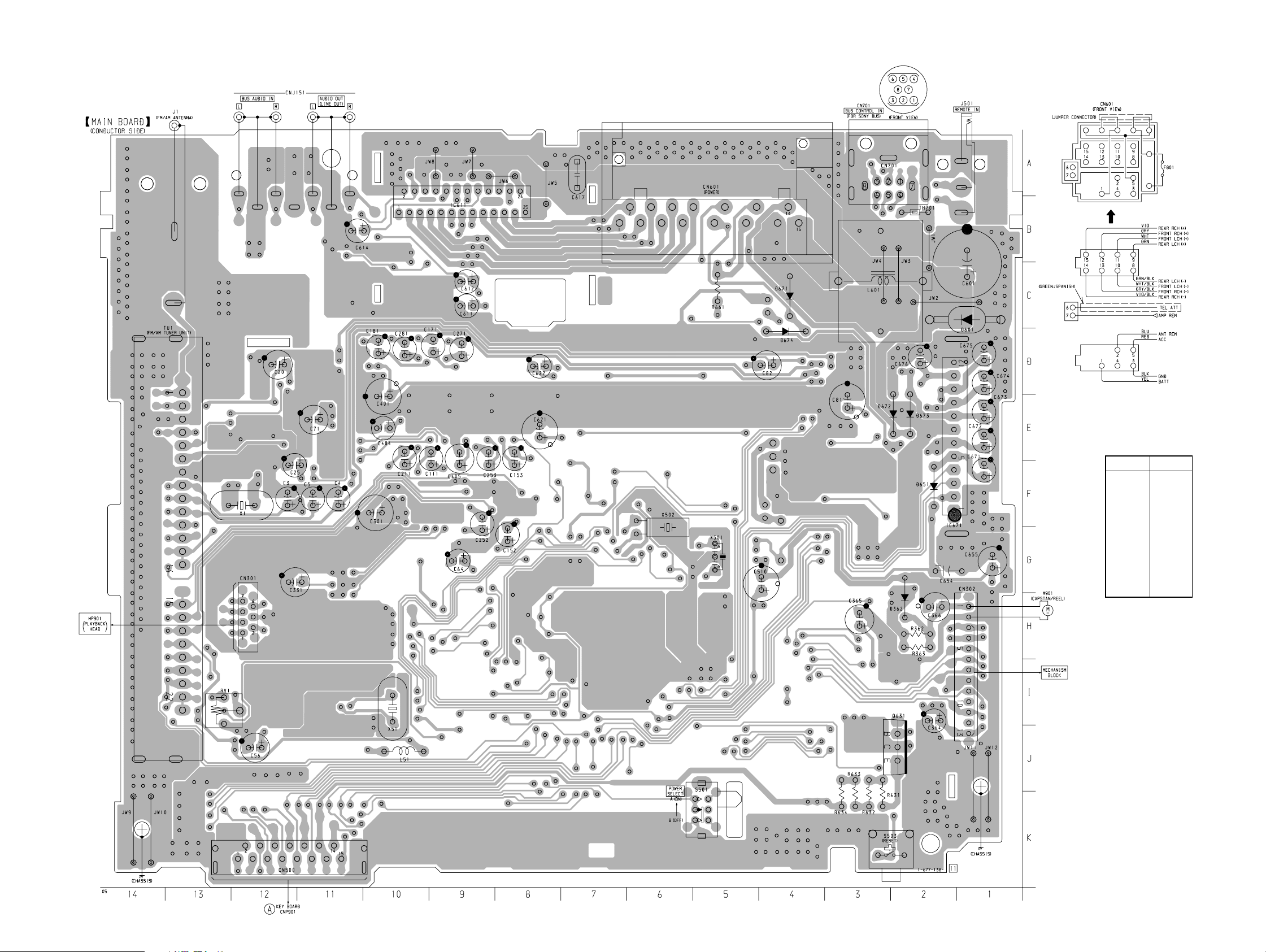
2-4. PRINTED WIRING BOARD – MAIN Board (Conductor Side) –
XR-3100R/C33R
• Semiconductor
Location
Ref. No. Location
D362 H-2
D601 C-1
D651 F-2
D671 C-4
D672 E-2
D673 E-2
D674 D-4
IC611 A-9
IC671 E-2
Q631 J-2
55
Page 6

XR-3100R/C33R
2-5. SCHEMATIC DIAGRAM – MAIN Board (1/3) –
(Page
8)
(Page
7)
(Page 8)
66
Page 7

2-6. SCHEMATIC DIAGRAM – MAIN Board (2/3) –
XR-3100R/C33R
(Page
6)
(Page 8)
77
Page 8

XR-3100R/C33R
2-7. SCHEMATIC DIAGRAM – MAIN Board (3/3) –
(Page 6)
(Page 7)
(Page 6)
88
Page 9

2-8. EXPLODED VIEWS
Page Former type New type
Ref. No. Part No. Description Remark
* 5 A-3326-073-A MAIN BOARD, COMPLETE (AMBER)
* 5 A-3326-106-A MAIN BOARD, COMPLETE (GREEN)
35
Ref. No. Part No. Description Remark
* 5 A-3326-073-A MAIN BOARD, COMPLETE (AMBER)
* 5 A-3326-106-A MAIN BOARD, COMPLETE
* 5 A-3326-689-A MAIN BOARD, COMPLETE
(GREEN: SPANISH)
(GREEN: EXCEPT SPANISH)
44
14 1-777-989-21 CORD (WITH CONNECTOR) (AMP REM)
14 1-777-989-21 CORD (WITH CONNECTOR) (AMP REM)
506 1-777-989-21 CORD (WITH CONNECTOR) (AMP REM)
14 1-777-989-21 CORD (WITH CONNECTOR) (AMP REM)
(GREEN: EXCEPT SPANISH)
14 1-777-989-41 CORD (WITH CONNECTOR)
(AMP REM/TEL ATT) (GREEN: SPANISH)
14 1-777-989-21 CORD (WITH CONNECTOR) (AMP REM)
(GREEN: EXCEPT SPANISH)
14 1-777-989-41 CORD (WITH CONNECTOR)
(AMP REM/TEL ATT) (GREEN: SPANISH)
506 1-777-989-21 CORD (WITH CONNECTOR) (AMP REM)
(GREEN: EXCEPT SPANISH)
506 1-777-989-41 CORD (WITH CONNECTOR)
(AMP REM/TEL ATT) (GREEN: SPANISH)
9
Page 10

MAIN
2-9. ELECTRICAL PARTS LIST
NOTE:
• Due to standardization, replacements in the
parts list may be different from the parts specified in the diagrams or the components used
on the set.
• -XX and -X mean standardized parts, so they
may have some difference from the original
one.
• RESISTORS
All resistors are in ohms.
METAL: Metal-film resistor.
METAL OXIDE: Metal oxide-film resistor.
F: nonflammable
Ref. No. Part No. Description Remark Ref. No. Part No. Description Remark
* A-3326-073-A MAIN BOARD, COMPLETE (AMBER)
* A-3326-106-A MAIN BOARD, COMPLETE (GREEN: SPANISH)
* A-3326-689-A MAIN BOARD, COMPLETE
(GREEN: EXCEPT SPANISH)
**********************
* 3-019-147-01 BRACKET (IC) (M)
* 3-031-050-02 HEAT SINK
* 3-031-828-01 BRACKET (REG.IC)
7-685-793-09 SCREW +PTT 2.6X8 (S)
7-685-795-09 SCREW +PTT 2.6X12 (S)
< CAPACITOR >
C1 1-163-235-11 CERAMIC CHIP 22PF 5% 50V
C2 1-163-133-00 CERAMIC CHIP 470PF 5% 50V
C3 1-124-233-11 ELECT 10uF 20% 16V
C4 1-124-233-11 ELECT 10uF 20% 16V
C5 1-124-233-11 ELECT 10uF 20% 16V
C6 1-163-021-11 CERAMIC CHIP 0.01uF 10% 50V
C7 1-163-021-11 CERAMIC CHIP 0.01uF 10% 50V
C8 1-163-009-11 CERAMIC CHIP 0.001uF 10% 50V
C10 1-163-009-11 CERAMIC CHIP 0.001uF 10% 50V
C11 1-163-020-00 CERAMIC CHIP 0.0082uF 10% 50V
C12 1-163-809-11 CERAMIC CHIP 0.047uF 10% 25V
C13 1-109-982-11 CERAMIC CHIP 1uF 10% 10V
C14 1-163-809-11 CERAMIC CHIP 0.047uF 10% 25V
C15 1-163-251-11 CERAMIC CHIP 100PF 5% 50V
C16 1-163-021-11 CERAMIC CHIP 0.01uF 10% 50V
C17 1-163-251-11 CERAMIC CHIP 100PF 5% 50V
C18 1-163-251-11 CERAMIC CHIP 100PF 5% 50V
C19 1-163-059-00 CERAMIC CHIP 0.01uF 10% 50V
C20 1-124-234-00 ELECT 22uF 20% 16V
C21 1-163-091-00 CERAMIC CHIP 8PF 50V
C22 1-163-231-11 CERAMIC CHIP 15PF 5% 50V
C23 1-163-087-00 CERAMIC CHIP 4PF 50V
C24 1-163-133-00 CERAMIC CHIP 470PF 5% 50V
C25 1-124-233-11 ELECT 10uF 20% 16V
C26 1-163-009-11 CERAMIC CHIP 0.001uF 10% 50V
C27 1-164-004-11 CERAMIC CHIP 0.1uF 10% 25V
C33 1-163-133-00 CERAMIC CHIP 470PF 5% 50V
C34 1-163-133-00 CERAMIC CHIP 470PF 5% 50V
C51 1-164-004-11 CERAMIC CHIP 0.1uF 10% 25V
C52 1-164-004-11 CERAMIC CHIP 0.1uF 10% 25V
C53 1-163-229-11 CERAMIC CHIP 12PF 5% 50V
C54 1-163-229-11 CERAMIC CHIP 12PF 5% 50V
• Items marked “*” are not stocked since they
are seldom required for routine service.
Some delay should be anticipated when ordering these items.
• SEMICONDUCTORS
In each case, u: µ, for example:
uA. . : µA. . uPA. . : µPA. .
uPB. . : µPB. . uPC. . : µPC. .
uPD. . : µPD. .
• CAPACITORS
uF: µF
• COILS
uH: µH
C55 1-164-004-11 CERAMIC CHIP 0.1uF 10% 25V
C56 1-124-234-00 ELECT 22uF 20% 16V
C57 1-163-021-11 CERAMIC CHIP 0.01uF 10% 50V
C58 1-163-263-11 CERAMIC CHIP 330PF 5% 50V
C59 1-164-505-11 CERAMIC CHIP 2.2uF 16V
C60 1-163-135-00 CERAMIC CHIP 560PF 5% 50V
C61 1-164-161-11 CERAMIC CHIP 0.0022uF 10% 100V
C62 1-163-009-11 CERAMIC CHIP 0.001uF 10% 50V
C63 1-163-133-00 CERAMIC CHIP 470PF 5% 50V
C64 1-124-233-11 ELECT 10uF 20% 16V
C71 1-124-234-00 ELECT 22uF 20% 16V
C73 1-164-004-11 CERAMIC CHIP 0.1uF 10% 25V
C81 1-124-589-11 ELECT 47uF 20% 16V
C82 1-124-234-00 ELECT 22uF 20% 16V
C83 1-164-004-11 CERAMIC CHIP 0.1uF 10% 25V
C90 1-163-009-11 CERAMIC CHIP 0.001uF 10% 50V
C91 1-163-009-11 CERAMIC CHIP 0.001uF 10% 50V
C92 1-163-009-11 CERAMIC CHIP 0.001uF 10% 50V
C93 1-163-133-00 CERAMIC CHIP 470PF 5% 50V
C94 1-163-227-11 CERAMIC CHIP 10PF 0.5PF 50V
C95 1-107-823-11 CERAMIC CHIP 0.47uF 10% 16V
C96 1-163-809-11 CERAMIC CHIP 0.047uF 10% 25V
C97 1-164-004-11 CERAMIC CHIP 0.1uF 10% 25V
C98 1-164-004-11 CERAMIC CHIP 0.1uF 10% 25V
C101 1-163-263-11 CERAMIC CHIP 330PF 5% 50V
C102 1-163-263-11 CERAMIC CHIP 330PF 5% 50V
C105 1-163-021-11 CERAMIC CHIP 0.01uF 10% 50V
C107 1-164-489-11 CERAMIC CHIP 0.22uF 10% 16V
C108 1-163-009-11 CERAMIC CHIP 0.001uF 10% 50V
C110 1-163-007-11 CERAMIC CHIP 680PF 10% 50V
C111 1-126-163-11 ELECT 4.7uF 20% 50V
C121 1-164-489-11 CERAMIC CHIP 0.22uF 10% 16V
C122 1-163-989-11 CERAMIC CHIP 0.033uF 10% 25V
C123 1-163-037-11 CERAMIC CHIP 0.022uF 10% 25V
C135 1-163-227-11 CERAMIC CHIP 10PF 0.5PF 50V
C141 1-163-251-11 CERAMIC CHIP 100PF 5% 50V
C142 1-107-823-11 CERAMIC CHIP 0.47uF 10% 16V
C151 1-163-020-00 CERAMIC CHIP 0.0082uF 10% 50V
C152 1-124-257-00 ELECT 2.2uF 20% 50V
C153 1-124-257-00 ELECT 2.2uF 20% 50V
C171 1-126-163-11 ELECT 4.7uF 20% 50V
C173 1-164-489-11 CERAMIC CHIP 0.22uF 10% 16V
C174 1-163-251-11 CERAMIC CHIP 100PF 5% 50V
• Abbreviation
AMBER : Amber illumination type
GREEN : Green illumination type
When indicating parts by reference
number, please include the board.
10
Page 11

MAIN
Ref. No. Part No. Description Remark
C181 1-126-163-11 ELECT 4.7uF 20% 50V
C182 1-163-251-11 CERAMIC CHIP 100PF 5% 50V
C183 1-164-489-11 CERAMIC CHIP 0.22uF 10% 16V
C184 1-163-251-11 CERAMIC CHIP 100PF 5% 50V
C201 1-163-263-11 CERAMIC CHIP 330PF 5% 50V
C202 1-163-263-11 CERAMIC CHIP 330PF 5% 50V
C205 1-163-021-11 CERAMIC CHIP 0.01uF 10% 50V
C207 1-164-489-11 CERAMIC CHIP 0.22uF 10% 16V
C208 1-163-009-11 CERAMIC CHIP 0.001uF 10% 50V
C210 1-163-007-11 CERAMIC CHIP 680PF 10% 50V
C211 1-126-163-11 ELECT 4.7uF 20% 50V
C235 1-163-227-11 CERAMIC CHIP 10PF 0.5PF 50V
C241 1-163-251-11 CERAMIC CHIP 100PF 5% 50V
C242 1-107-823-11 CERAMIC CHIP 0.47uF 10% 16V
C251 1-163-020-00 CERAMIC CHIP 0.0082uF 10% 50V
C252 1-124-257-00 ELECT 2.2uF 20% 50V
C253 1-124-257-00 ELECT 2.2uF 20% 50V
C271 1-126-163-11 ELECT 4.7uF 20% 50V
C273 1-164-489-11 CERAMIC CHIP 0.22uF 10% 16V
C274 1-163-251-11 CERAMIC CHIP 100PF 5% 50V
C281 1-126-163-11 ELECT 4.7uF 20% 50V
C282 1-163-251-11 CERAMIC CHIP 100PF 5% 50V
C283 1-164-489-11 CERAMIC CHIP 0.22uF 10% 16V
C284 1-163-251-11 CERAMIC CHIP 100PF 5% 50V
C301 1-124-584-00 ELECT 100uF 20% 10V
C302 1-163-251-11 CERAMIC CHIP 100PF 5% 50V
C303 1-107-823-11 CERAMIC CHIP 0.47uF 10% 16V
C304 1-163-021-11 CERAMIC CHIP 0.01uF 10% 50V
C305 1-164-004-11 CERAMIC CHIP 0.1uF 10% 25V
C306 1-163-021-11 CERAMIC CHIP 0.01uF 10% 50V
C331 1-124-234-00 ELECT 22uF 20% 16V
C361 1-165-319-11 CERAMIC CHIP 0.1uF 50V
C362 1-165-319-11 CERAMIC CHIP 0.1uF 50V
C363 1-163-021-11 CERAMIC CHIP 0.01uF 10% 50V
C364 1-126-157-11 ELECT 10uF 20% 16V
C365 1-124-234-00 ELECT 22uF 20% 16V
C366 1-126-933-11 ELECT 100uF 20% 16V
C401 1-124-584-00 ELECT 100uF 20% 10V
C402 1-163-021-11 CERAMIC CHIP 0.01uF 10% 50V
C404 1-124-233-11 ELECT 10uF 20% 16V
C405 1-124-234-00 ELECT 22uF 20% 16V
C408 1-163-251-11 CERAMIC CHIP 100PF 5% 50V
C502 1-164-004-11 CERAMIC CHIP 0.1uF 10% 25V
C503 1-164-004-11 CERAMIC CHIP 0.1uF 10% 25V
C504 1-164-004-11 CERAMIC CHIP 0.1uF 10% 25V
C505 1-164-004-11 CERAMIC CHIP 0.1uF 10% 25V
C506 1-163-102-00 CERAMIC CHIP 24PF 5% 50V
C507 1-163-235-11 CERAMIC CHIP 22PF 5% 50V
C509 1-163-021-11 CERAMIC CHIP 0.01uF 10% 50V
C510 1-124-584-00 ELECT 100uF 20% 10V
C511 1-164-004-11 CERAMIC CHIP 0.1uF 10% 25V
C527 1-165-319-11 CERAMIC CHIP 0.1uF 50V
C571 1-163-251-11 CERAMIC CHIP 100PF 5% 50V
(GREEN: SPANISH)
C601 1-107-885-31 ELECT 3300uF 20% 16V
C602 1-163-251-11 CERAMIC CHIP 100PF 5% 50V
C603 1-163-251-11 CERAMIC CHIP 100PF 5% 50V
C611 1-124-233-11 ELECT 10uF 20% 16V
Ref. No. Part No. Description Remark
C612 1-124-233-11 ELECT 10uF 20% 16V
C613 1-109-982-11 CERAMIC CHIP 1uF 10% 10V
C614 1-107-909-11 ELECT 47uF 20% 16V
C616 1-107-823-11 CERAMIC CHIP 0.47uF 10% 16V
C617 1-136-165-00 FILM 0.1uF 5% 50V
C621 1-124-589-11 ELECT 47uF 20% 16V
C622 1-124-257-00 ELECT 2.2uF 20% 50V
C623 1-109-982-11 CERAMIC CHIP 1uF 10% 10V
C631 1-164-222-11 CERAMIC CHIP 0.22uF 25V
C632 1-164-222-11 CERAMIC CHIP 0.22uF 25V
C641 1-163-009-11 CERAMIC CHIP 0.001uF 10% 50V
C653 1-163-021-11 CERAMIC CHIP 0.01uF 10% 50V
C654 1-125-701-11 DOUBLE LAYER 0.047F 5.5V
C655 1-126-933-11 ELECT 100uF 20% 16V
C661 1-109-982-11 CERAMIC CHIP 1uF 10% 10V
C671 1-126-157-11 ELECT 10uF 20% 16V
C672 1-126-157-11 ELECT 10uF 20% 16V
C673 1-126-157-11 ELECT 10uF 20% 16V
C674 1-126-157-11 ELECT 10uF 20% 16V
C675 1-126-157-11 ELECT 10uF 20% 16V
C676 1-126-157-11 ELECT 10uF 20% 16V
C701 1-163-021-11 CERAMIC CHIP 0.01uF 10% 50V
C702 1-164-004-11 CERAMIC CHIP 0.1uF 10% 25V
C703 1-163-037-11 CERAMIC CHIP 0.022uF 10% 25V
C704 1-163-077-00 CERAMIC CHIP 0.1uF 10% 25V
< CONNECTOR >
CN301 1-766-260-11 CONNECTOR, FFC/FPC (ZIF) 7P
* CN302 1-506-995-11 PIN, CONNECTOR (PC BOARD) 13P
CN500 1-785-772-11 PLUG, CONNECTOR 15P
CN601 1-785-761-11 PIN, CONNECTOR (ISO) (POWER)
CN701 1-580-907-31 PLUG, CONNECTOR (BUS CONTROL IN)
< JACK >
CNJ151 1-774-699-12 JACK, PIN 4P (BUS AUDIO IN, AUDIO OUT)
< DIODE >
D1 8-719-991-65 DIODE SB02W03C-TB
D61 8-719-422-12 DIODE UDZ-TE-17-3.9B
D71 8-719-158-15 DIODE UDZ-TE-17-5.6B
D81 8-719-977-28 DIODE UDZ-TE-17-10B
D90 8-719-073-01 DIODE MA111-TX
D91 8-719-073-01 DIODE MA111-TX
D92 8-719-976-99 DIODE UDZ-TE-17-5.1B
D93 8-719-422-12 DIODE UDZ-TE-17-3.9B
D361 8-719-977-22 DIODE UDZ-TE-17-9.1B
D362 8-719-911-19 DIODE 1SS119-25TD
D441 8-719-056-82 DIODE UDZ-TE-17-6.2B
D481 8-719-056-82 DIODE UDZ-TE-17-6.2B
D501 8-719-914-44 DIODE DAP202K-T-146
D551 8-719-056-82 DIODE UDZ-TE-17-6.2B
D552 8-719-056-82 DIODE UDZ-TE-17-6.2B
D553 8-719-056-82 DIODE UDZ-TE-17-6.2B
D554 8-719-056-82 DIODE UDZ-TE-17-6.2B
D555 8-719-056-93 DIODE UDZ-TE-17-18B
D556 8-719-056-82 DIODE UDZ-TE-17-6.2B
D557 8-719-056-82 DIODE UDZ-TE-17-6.2B
11
Page 12

MAIN
Ref. No. Part No. Description Remark
D558 8-719-056-82 DIODE UDZ-TE-17-6.2B
D559 8-719-056-82 DIODE UDZ-TE-17-6.2B
D561 8-719-056-82 DIODE UDZ-TE-17-6.2B
D562 8-719-056-82 DIODE UDZ-TE-17-6.2B
D571 8-719-073-01 DIODE MA111-TX (GREEN: SPANISH)
D601 8-719-049-38 DIODE 1N5404TU
D602 8-719-056-93 DIODE UDZ-TE-17-18B
D603 8-719-056-93 DIODE UDZ-TE-17-18B
D604 8-719-056-82 DIODE UDZ-TE-17-6.2B
D605 8-719-056-82 DIODE UDZ-TE-17-6.2B (GREEN: SPANISH)
D611 8-719-053-18 DIODE 1SR154-400TE-25
D612 8-719-053-18 DIODE 1SR154-400TE-25
D613 8-719-053-18 DIODE 1SR154-400TE-25
D614 8-719-053-18 DIODE 1SR154-400TE-25
D615 8-719-053-18 DIODE 1SR154-400TE-25
D616 8-719-053-18 DIODE 1SR154-400TE-25
D617 8-719-053-18 DIODE 1SR154-400TE-25
D618 8-719-053-18 DIODE 1SR154-400TE-25
D621 8-719-422-12 DIODE UDZ-TE-17-3.9B
D622 8-719-073-01 DIODE MA111-TX
D623 8-719-977-22 DIODE UDZ-TE-17-9.1B
D624 8-719-073-01 DIODE MA111-TX
D631 8-719-158-49 DIODE UDZ-TE-17-12B
D651 8-719-911-19 DIODE 1SS119-25TD
D653 8-719-073-01 DIODE MA111-TX
D661 8-719-073-01 DIODE MA111-TX
D662 8-719-056-85 DIODE UDZ-TE-17-8.2B
D671 8-719-970-02 DIODE 1SR139-400T-32
D672 8-719-970-02 DIODE 1SR139-400T-32
D673 8-719-970-02 DIODE 1SR139-400T-32
D674 8-719-970-02 DIODE 1SR139-400T-32
D701 8-719-056-93 DIODE UDZ-TE-17-18B
D702 8-719-017-62 DIODE MA8068-L-TX
D703 8-719-056-82 DIODE UDZ-TE-17-6.2B
D704 8-719-056-93 DIODE UDZ-TE-17-18B
D705 8-719-056-93 DIODE UDZ-TE-17-18B
D706 8-719-072-70 DIODE MA2ZD14001S0
< FERRITE BEAD >
FB501 1-414-233-22 INDUCTOR, FERRITE BEAD
< IC >
IC1 8-759-586-59 IC TB2118F-EL-S
IC51 8-759-492-59 IC SAA6588T-118
IC90 8-759-909-71 IC BA4558F
IC301 8-752-079-78 IC CXA2509AQ-T4
IC361 8-759-823-87 IC LB1638M
IC401 8-759-572-10 IC TDA7462D013TR
IC501 8-759-683-39 IC MB90574BPMT-G-299-BND
IC611 8-759-486-44 IC TDA7386
IC652 8-759-574-61 IC XC61AN4302MR
IC671 8-759-347-50 IC BA3918-V3
IC701 8-759-449-89 IC BA8270F-E2
< JACK >
J1 1-764-808-21 JACK (ANT) (FM/AM ANTENNA)
J501 1-566-822-41 JACK (REMOTE IN)
Ref. No. Part No. Description Remark
< SHORT >
JC1 1-216-295-00 SHORT 0
JC301 1-216-295-00 SHORT 0
JC503 1-216-295-00 SHORT 0
< COIL >
L1 1-410-989-11 INDUCTOR CHIP 0.47uH
L51 1-410-509-11 INDUCTOR 10uH
L601 1-419-101-11 COIL, CHOKE (TOROIDAL-S)
< TRANSISTOR >
Q51 8-729-120-28 TRANSISTOR 2SC2412K-T-146-QR
Q61 8-729-921-25 TRANSISTOR FMC2-T148
Q71 8-729-015-11 TRANSISTOR 2SD1802FAST-TL
Q81 8-729-120-28 TRANSISTOR 2SC2412K-T-146-QR
Q82 8-729-921-25 TRANSISTOR FMC2-T148
Q90 8-729-900-53 TRANSISTOR DTC114EKA-T146
Q121 8-729-920-21 TRANSISTOR DTC314TK-T-146
Q151 8-729-920-21 TRANSISTOR DTC314TK-T-146
Q171 8-729-920-21 TRANSISTOR DTC314TK-T-146
Q181 8-729-920-21 TRANSISTOR DTC314TK-T-146
Q251 8-729-920-21 TRANSISTOR DTC314TK-T-146
Q271 8-729-920-21 TRANSISTOR DTC314TK-T-146
Q281 8-729-920-21 TRANSISTOR DTC314TK-T-146
Q361 8-729-015-11 TRANSISTOR 2SD1802FAST-TL
Q362 8-729-921-25 TRANSISTOR FMC2-T148
Q364 8-729-106-60 TRANSISTOR 2SB1132-T100-R
Q365 8-729-900-53 TRANSISTOR DTC114EKA-T146
Q571 8-729-120-28 TRANSISTOR 2SC2412K-T-146-QR
(GREEN: SPANISH)
Q621 8-729-027-23 TRANSISTOR DTA114EKA-T146
Q622 8-729-021-94 TRANSISTOR 2SK1657-T1B
Q631 8-729-423-99 TRANSISTOR 2SD2137-OP-TA
Q633 8-729-921-25 TRANSISTOR FMC2-T148
Q651 8-729-027-23 TRANSISTOR DTA114EKA-T146
Q652 8-729-027-23 TRANSISTOR DTA114EKA-T146
Q661 8-729-120-28 TRANSISTOR 2SC2412K-T-146-QR
Q701 8-729-900-53 TRANSISTOR DTC114EKA-T146
< RESISTOR >
R1 1-216-049-11 RES-CHIP 1K 5% 1/10W
R2 1-216-029-00 METAL CHIP 150 5% 1/10W
R3 1-216-065-00 RES-CHIP 4.7K 5% 1/10W
R6 1-216-073-00 METAL CHIP 10K 5% 1/10W
R7 1-216-073-00 METAL CHIP 10K 5% 1/10W
R8 1-216-073-00 METAL CHIP 10K 5% 1/10W
R11 1-216-061-00 METAL CHIP 3.3K 5% 1/10W
R12 1-216-067-00 METAL CHIP 5.6K 5% 1/10W
R13 1-216-025-00 RES-CHIP 100 5% 1/10W
R14 1-216-067-00 METAL CHIP 5.6K 5% 1/10W
R15 1-216-025-00 RES-CHIP 100 5% 1/10W
R16 1-216-073-00 METAL CHIP 10K 5% 1/10W
R51 1-216-097-00 RES-CHIP 100K 5% 1/10W
R52 1-216-057-00 METAL CHIP 2.2K 5% 1/10W
R53 1-216-113-00 METAL CHIP 470K 5% 1/10W
R54 1-216-049-11 RES-CHIP 1K 5% 1/10W
12
Page 13

MAIN
Ref. No. Part No. Description Remark
R55 1-216-061-00 METAL CHIP 3.3K 5% 1/10W
R56 1-216-041-00 METAL CHIP 470 5% 1/10W
R57 1-216-037-00 METAL CHIP 330 5% 1/10W
R58 1-216-037-00 METAL CHIP 330 5% 1/10W
R59 1-216-001-00 METAL CHIP 10 5% 1/10W
R60 1-216-009-00 RES-CHIP 22 5% 1/10W
R61 1-216-037-00 METAL CHIP 330 5% 1/10W
R62 1-216-045-00 METAL CHIP 680 5% 1/10W
R71 1-216-057-00 METAL CHIP 2.2K 5% 1/10W
R81 1-216-057-00 METAL CHIP 2.2K 5% 1/10W
R90 1-216-057-00 METAL CHIP 2.2K 5% 1/10W
R91 1-216-057-00 METAL CHIP 2.2K 5% 1/10W
R92 1-216-061-00 METAL CHIP 3.3K 5% 1/10W
R93 1-216-097-00 RES-CHIP 100K 5% 1/10W
R94 1-216-065-00 RES-CHIP 4.7K 5% 1/10W
R95 1-216-121-00 RES-CHIP 1M 5% 1/10W
R96 1-216-065-00 RES-CHIP 4.7K 5% 1/10W
R97 1-216-049-11 RES-CHIP 1K 5% 1/10W
R101 1-216-097-00 RES-CHIP 100K 5% 1/10W
R102 1-216-097-00 RES-CHIP 100K 5% 1/10W
R105 1-216-109-00 METAL CHIP 330K 5% 1/10W
R106 1-216-077-00 RES-CHIP 15K 5% 1/10W
R107 1-216-079-00 METAL CHIP 18K 5% 1/10W
R108 1-216-073-00 METAL CHIP 10K 5% 1/10W
R109 1-216-077-00 RES-CHIP 15K 5% 1/10W
R110 1-216-041-00 METAL CHIP 470 5% 1/10W
R121 1-216-065-00 RES-CHIP 4.7K 5% 1/10W
R141 1-216-057-00 METAL CHIP 2.2K 5% 1/10W
R142 1-216-073-00 METAL CHIP 10K 5% 1/10W
R151 1-216-077-00 RES-CHIP 15K 5% 1/10W
R152 1-216-085-00 METAL CHIP 33K 5% 1/10W
R171 1-216-033-00 METAL CHIP 220 5% 1/10W
R172 1-216-065-00 RES-CHIP 4.7K 5% 1/10W
R173 1-216-089-00 RES-CHIP 47K 5% 1/10W
Ref. No. Part No. Description Remark
R284 1-216-121-00 RES-CHIP 1M 5% 1/10W
R301 1-208-812-11 RES-CHIP 18K 2% 1/10W
R302 1-216-065-00 RES-CHIP 4.7K 5% 1/10W
R303 1-216-077-00 RES-CHIP 15K 5% 1/10W
R304 1-216-105-00 RES-CHIP 220K 5% 1/10W
R305 1-216-001-00 METAL CHIP 10 5% 1/10W
R361 1-216-049-11 RES-CHIP 1K 5% 1/10W
R362 1-249-389-11 CARBON 4.7 5% 1/4W
R363 1-249-389-11 CARBON 4.7 5% 1/4W
R364 1-216-073-00 METAL CHIP 10K 5% 1/10W
R365 1-216-065-00 RES-CHIP 4.7K 5% 1/10W
R504 1-216-057-00 METAL CHIP 2.2K 5% 1/10W
R505 1-216-057-00 METAL CHIP 2.2K 5% 1/10W
R506 1-216-057-00 METAL CHIP 2.2K 5% 1/10W
R508 1-216-073-00 METAL CHIP 10K 5% 1/10W
R509 1-216-097-00 RES-CHIP 100K 5% 1/10W
R511 1-216-097-00 RES-CHIP 100K 5% 1/10W
R512 1-216-097-00 RES-CHIP 100K 5% 1/10W
R518 1-216-097-00 RES-CHIP 100K 5% 1/10W
R519 1-216-097-00 RES-CHIP 100K 5% 1/10W
R520 1-216-097-00 RES-CHIP 100K 5% 1/10W
R522 1-216-097-00 RES-CHIP 100K 5% 1/10W
R523 1-216-097-00 RES-CHIP 100K 5% 1/10W
R524 1-216-057-00 METAL CHIP 2.2K 5% 1/10W
R525 1-216-057-00 METAL CHIP 2.2K 5% 1/10W
R526 1-216-097-00 RES-CHIP 100K 5% 1/10W
R527 1-208-806-11 RES-CHIP 10K 0.5% 1/10W
R529 1-216-073-00 METAL CHIP 10K 5% 1/10W
R531 1-216-085-00 METAL CHIP 33K 5% 1/10W
(GREEN: SPANISH)
R532 1-216-073-00 METAL CHIP 10K 5% 1/10W
(GREEN: SPANISH)
R533 1-216-073-00 METAL CHIP 10K 5% 1/10W
(GREEN: SPANISH)
R174 1-216-121-00 RES-CHIP 1M 5% 1/10W
R181 1-216-033-00 METAL CHIP 220 5% 1/10W
R182 1-216-065-00 RES-CHIP 4.7K 5% 1/10W
R183 1-216-089-00 RES-CHIP 47K 5% 1/10W
R184 1-216-121-00 RES-CHIP 1M 5% 1/10W
R201 1-216-097-00 RES-CHIP 100K 5% 1/10W
R202 1-216-097-00 RES-CHIP 100K 5% 1/10W
R205 1-216-109-00 METAL CHIP 330K 5% 1/10W
R206 1-216-077-00 RES-CHIP 15K 5% 1/10W
R207 1-216-079-00 METAL CHIP 18K 5% 1/10W
R208 1-216-073-00 METAL CHIP 10K 5% 1/10W
R209 1-216-077-00 RES-CHIP 15K 5% 1/10W
R210 1-216-041-00 METAL CHIP 470 5% 1/10W
R241 1-216-057-00 METAL CHIP 2.2K 5% 1/10W
R242 1-216-073-00 METAL CHIP 10K 5% 1/10W
R251 1-216-077-00 RES-CHIP 15K 5% 1/10W
R252 1-216-085-00 METAL CHIP 33K 5% 1/10W
R271 1-216-033-00 METAL CHIP 220 5% 1/10W
R272 1-216-065-00 RES-CHIP 4.7K 5% 1/10W
R273 1-216-089-00 RES-CHIP 47K 5% 1/10W
R274 1-216-121-00 RES-CHIP 1M 5% 1/10W
R281 1-216-033-00 METAL CHIP 220 5% 1/10W
R282 1-216-065-00 RES-CHIP 4.7K 5% 1/10W
R283 1-216-089-00 RES-CHIP 47K 5% 1/10W
R534 1-216-097-00 RES-CHIP 100K 5% 1/10W
(GREEN: SPANISH)
R535 1-216-097-00 RES-CHIP 100K 5% 1/10W
R536 1-216-097-00 RES-CHIP 100K 5% 1/10W
(GREEN)
R537 1-216-097-00 RES-CHIP 100K 5% 1/10W
(AMBER)
R539 1-216-097-00 RES-CHIP 100K 5% 1/10W
R540 1-216-097-00 RES-CHIP 100K 5% 1/10W
R542 1-216-089-00 RES-CHIP 47K 5% 1/10W
R551 1-208-806-11 RES-CHIP 10K 0.5% 1/10W
R552 1-208-806-11 RES-CHIP 10K 0.5% 1/10W
R553 1-216-025-00 RES-CHIP 100 5% 1/10W
R554 1-216-025-00 RES-CHIP 100 5% 1/10W
R555 1-216-097-00 RES-CHIP 100K 5% 1/10W
R556 1-216-097-00 RES-CHIP 100K 5% 1/10W
R558 1-216-025-00 RES-CHIP 100 5% 1/10W
R559 1-216-025-00 RES-CHIP 100 5% 1/10W
R560 1-216-025-00 RES-CHIP 100 5% 1/10W
R561 1-216-025-00 RES-CHIP 100 5% 1/10W
R571 1-216-097-00 RES-CHIP 100K 5% 1/10W
(GREEN: EXCEPT SPANISH)
R611 1-216-049-11 RES-CHIP 1K 5% 1/10W
R612 1-216-049-11 RES-CHIP 1K 5% 1/10W
13
Page 14

XR-3100R/C33R
MAIN
Ref. No. Part No. Description Remark
R621 1-216-017-00 RES-CHIP 47 5% 1/10W
R622 1-216-295-00 SHORT 0
R623 1-216-073-00 METAL CHIP 10K 5% 1/10W
R624 1-216-049-11 RES-CHIP 1K 5% 1/10W
R631 1-249-383-11 CARBON 1.5 5% 1/6W
R632 1-249-383-11 CARBON 1.5 5% 1/6W
R633 1-249-383-11 CARBON 1.5 5% 1/6W
R634 1-249-383-11 CARBON 1.5 5% 1/6W
R636 1-216-037-00 METAL CHIP 330 5% 1/10W
R641 1-216-097-00 RES-CHIP 100K 5% 1/10W
R642 1-216-113-00 METAL CHIP 470K 5% 1/10W
R651 1-216-113-00 METAL CHIP 470K 5% 1/10W
R652 1-216-097-00 RES-CHIP 100K 5% 1/10W
R653 1-208-806-11 RES-CHIP 10K 0.5% 1/10W
R654 1-216-073-00 METAL CHIP 10K 5% 1/10W
R655 1-216-025-00 RES-CHIP 100 5% 1/10W
R656 1-216-025-00 RES-CHIP 100 5% 1/10W
R661 1-249-421-11 CARBON 2.2K 5% 1/4W
R662 1-216-081-00 METAL CHIP 22K 5% 1/10W
R663 1-216-089-00 RES-CHIP 47K 5% 1/10W
R664 1-216-089-00 RES-CHIP 47K 5% 1/10W
R683 1-216-089-00 RES-CHIP 47K 5% 1/10W
R701 1-216-017-00 RES-CHIP 47 5% 1/10W
R702 1-216-073-00 METAL CHIP 10K 5% 1/10W
R703 1-216-025-00 RES-CHIP 100 5% 1/10W
Ref. No. Part No. Description Remark
R704 1-216-025-00 RES-CHIP 100 5% 1/10W
< COMPOSITION CIRCUIT BLOCK >
RB601 1-233-413-11 RES, CHIP NETWORK 2.2K (3216)
RB602 1-233-810-21 RES, NETWORK 100K (3216)
< VARIABLE RESISTOR >
RV1 1-223-836-11 RES, ADJ, CARBON 220K
< SWITCH >
S501 1-571-478-11 SWITCH, SLIDE (POWER SELECT)
S503 1-692-431-21 SWITCH, TACTILE (RESET)
< THERMISTOR >
TH701 1-801-792-21 THERMISTOR, POSITIVE
< TUNER >
TU1 1-693-440-24 TUNER UNIT (FM/AM TUNER UNIT)
< VIBRATOR >
X1 1-781-246-21 VIBRATOR, CRYSTAL (10.25MHz)
X51 1-579-242-41 VIBRATOR, CRYSTAL (4.332MHz)
X501 1-767-833-21 VIBRATOR, CERAMIC (3.68MHz)
X502 1-567-098-41 VIBRATOR, CRYSTAL (32.768kHz)
**************************************************************
9-870-047-81
14
Sony Corporation
Audio Entertainment Group
Printed in Japan C 2000. 7
2000G0541-1
Published by ME General Engineering Dept.
 Loading...