

Page 1
XP-ER800/ER800N/ER800R
SERVICE MANUAL
Ver 1.3 2003. 12
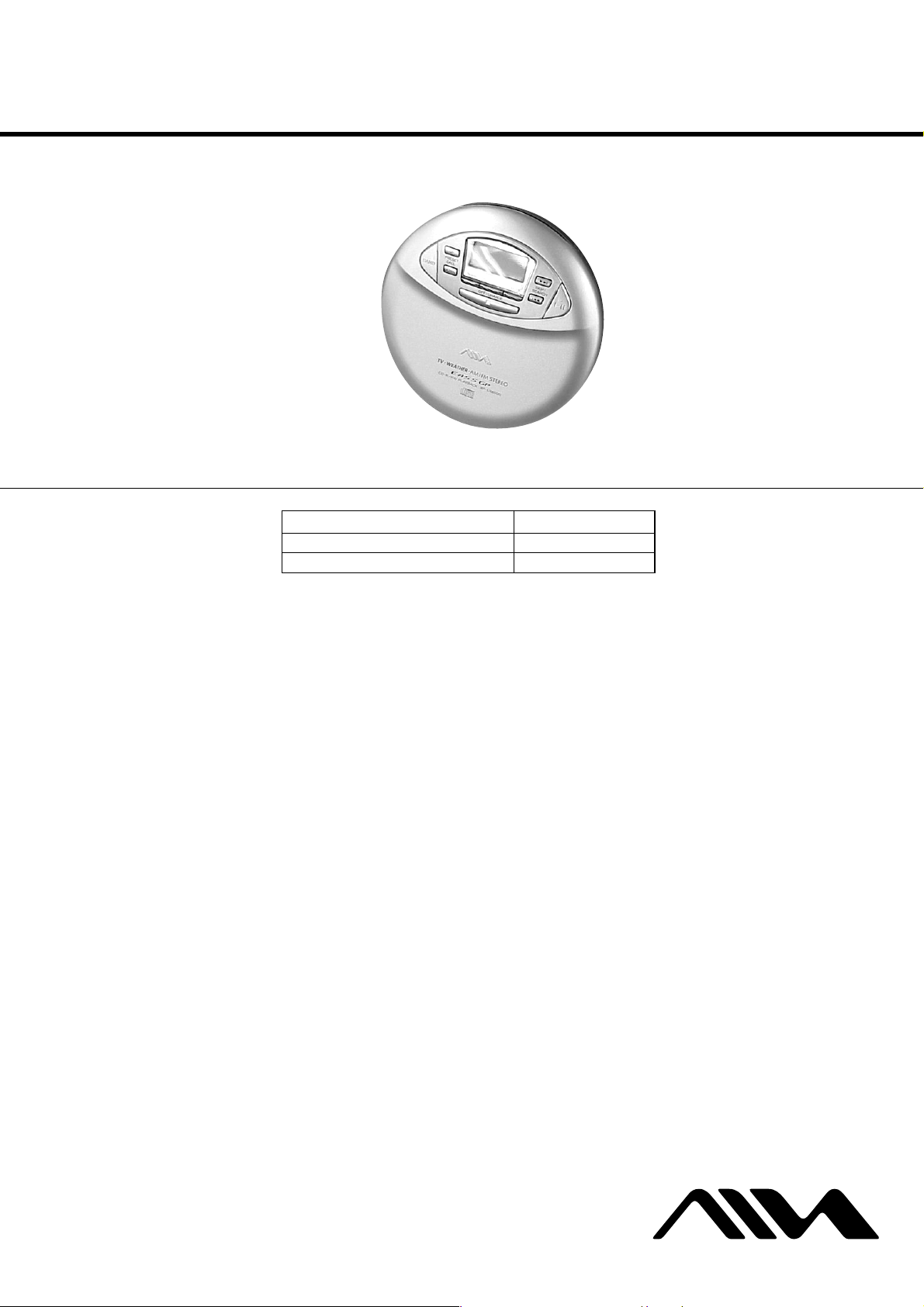
Photo : XP-ER800
Model Name Using Similar Mechanism D-EJ985
CD Mechanism Type CDM-3325ER
Optical Pick-up Name DAX-25E
SPECIFICATIONS
System
Compact disc digital audio system
Laser diode properties
Material: GaAlAs
Wavelength: λ = 780 nm
Emission duration: Continuous
Laser output: Less than 44.6 µW (This output is the value
measured at a distance of 200 mm from the objective lens
surface on the optical pick-up block with 7 mm aperture.)
Frequency range
10 kHz step:
US, CND Models
TV: 2 - 13 ch
WB (weather band): 1 - 7 ch
FM: 87.5 - 108.0 MHz
AM: 530 - 1 710 kHz
E13, AUS, HK, TW Models
FM: 87.5 - 108.0 MHz
AM: 530 - 1 710 kHz
9 kHz step:
US, CND Models
TV: 2 - 13 ch
WB (weather band): 1 - 7 ch
FM: 87.5 - 108.0 MHz
AM: 531 - 1 602 kHz
AEP Model
FM: 87.5 - 108.0 MHz
AM: 531 - 1 602 kHz
E13, AUS, HK, TW Models
FM: 87.5 - 108.0 MHz
AM: 531 - 1 602 kHz
Power requirements
• Two LR6 (size AA) batteries (not supplied): 3 V DC
• AC power adaptor (DC IN 4.5 V jack):
• Two Ni-MH rechargeable batteries (size AA): 1.2V × 2 DC
Dimensions (w/h/d) (without projecting
parts and controls)
Approx. 136.0 × 20.4 × 139.0 mm (5 3⁄
Mass (excluding accessories)
Approx. 200 g (7 oz)
Operating temperature
5°C – 35°C (41°F – 95°F)
Design and specifications are subject to change without
notice.
US, CND, TW Models
120 V, 60 Hz
AEP Model
220 - 230 V, 50 Hz
E13 Model
220 - 230 V, 50/60 Hz
AUS Model
240 V, 50/60 Hz
HK Model
230 V, 50 Hz
US Model
XP-ER800/ER800N
Canadian Model
XP-ER800
AEP Model
XP-ER800/ER800R
UK Model
XP-ER800R
E Model
XP-ER800/ER800R
Australian Model
XP-ER800
• Abbreviation
AUS : Australian model
CND: Canadian model
E13 : 220 – 230 V AC area in E model
HK : Hong Kong model
TW : Taiwan model
× 13⁄16 × 5 1⁄2 in.)
8
9-877-194-04
2003L16-1
© 2003.12
PORTABLE CD PLAYER
Sony Corporation
Personal Audio Company
Published by Sony Engineering Corporation
Page 2
XP-ER800/ER800N/ER800R
d
e
Ver 1.1 2003.06
TABLE OF CONTENTS
1. SERVICING NOTE ·························································· 3
2. GENERAL ·········································································· 4
3. DISASSEMBLY
3-1. Cabinet (REAR) Section ··············································· 6
3-2. Cabinet (Front) Sub Section ·········································· 7
3-3. Upper Lid ······································································8
3-4. CD Mechanism Deck (CDM-3325ER) ························· 9
3-5. MAIN Board ······························································· 10
3-6. Motor (turn table) Assy (M902),
Optical Pick-Up Assy ·················································· 11
4. ELECTRICAL ADJUSTMENT ·································· 12
5. DIAGRAMS······································································ 17
5-1. Block Diagram – Main Section – ······························· 18
5-2. Block Diagram – TUNER (4Band) Section – ············ 19
5-3. Block Diagram – TUNER (2Band) Section – ············· 20
5-4. Printed Wiring Board
– MAIN Board (4Band)(Side A) –······························ 21
5-5. Printed Wiring Board
– MAIN Board (4Band)(Side B) – ······························ 22
5-6. Printed Wiring Board
– MAIN Board (2Band)(Side A) –······························ 23
5-7. Printed Wiring Board
– MAIN Board (2Band)(Side B) – ······························ 24
5-8. Schematic Diagram – MAIN Board (1/6) – ················ 25
5-9. Schematic Diagram – MAIN Board (2/6) – ················ 26
5-10.Schematic Diagram – MAIN Board (3/6) – ················ 27
5-11.Schematic Diagram – MAIN Board (4/6) – ················ 28
5-12.Schematic Diagram – MAIN Board (5/6) – ················ 29
5-13.Schematic Diagram – MAIN Board (6A/6) – ············· 30
5-14.Schematic Diagram – MAIN Board (6B/6) – ·············31
5-15.IC Block Diagram ·······················································32
5-16.IC Pin Function Description········································ 35
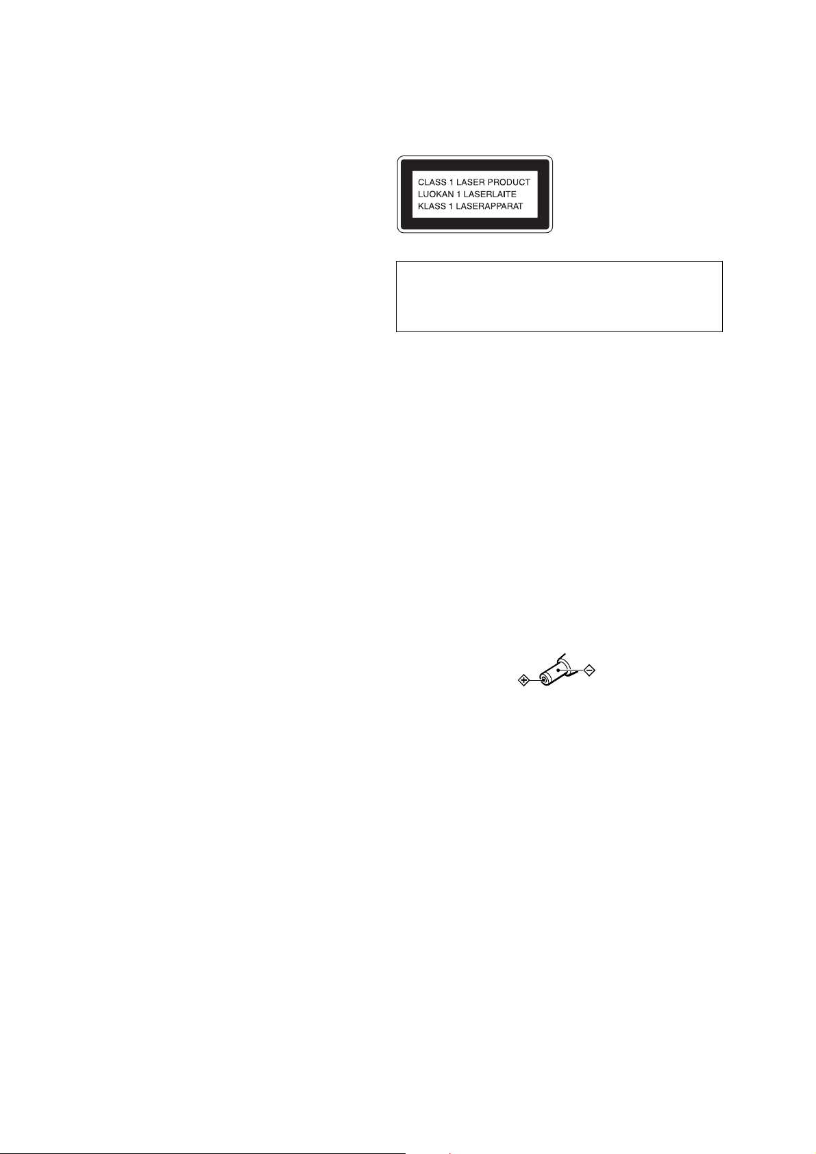
This appliance is classified as a CLASS 1 LASER product.
The CLASS 1 LASER PRODUCT MARKING is located on
the rear exterior.
CAUTION
Use of controls or adjustments or performance of procedures
other than those specified herein may result in hazardous
radiation exposure.
Flexible Circuit Board Repairing
•Keep the temperature of the soldering iron around 270 ˚C during repairing.
• Do not touch the soldering iron on the same conductor of the
circuit board (within 3 times).
• Be careful not to apply force on the conductor when soldering
or unsoldering.
Notes on chip component replacement
•Never reuse a disconnected chip component.
• Notice that the minus side of a tantalum capacitor may be damaged by heat.
On AC power adaptor
•
Use only the commercially-available AC power a
output is 4.5 V DC, 500 mA. Do not use any oth
It may cause a malfunction.
Polarity of the plug
6. EXPLODED VIEWS ······················································ 37
7. ELECTRICAL PARTS LIST······································· 40
SAFETY-RELATED COMPONENT WARNING!!
COMPONENTS IDENTIFIED BY MARK 0 OR DOTTED LINE WITH
MARK 0 ON THE SCHEMATIC DIAGRAMS AND IN THE PARTS
LIST ARE CRITICAL TO SAFE OPERATION. REPLACE THESE
COMPONENTS WITH SONY PARTS WHOSE PART NUMBERS
APPEAR AS SHOWN IN THIS MANUAL OR IN SUPPLEMENTS
PUBLISHED BY SONY.
ATTENTION AU COMPOSANT AYANT RAPPORT
À LA SÉCURITÉ!
LES COMPOSANTS IDENTIFÉS P AR UNE MARQUE 0 SUR LES
DIAGRAMMES SCHÉMA TIQUES ET LA LISTE DES PIÈCES SONT
CRITIQUES POUR LA SÉCURITÉ DE FONCTIONNEMENT. NE
REMPLACER CES COMPOSANTS QUE PAR DES PIÈSES SONY
DONT LES NUMÉROS SONT DONNÉS DANS CE MANUEL OU
DANS LES SUPPÉMENTS PUBLIÉS PAR SONY.
2
Page 3
SECTION 1
SERVICING NOTE
XP-ER800/ER800N/ER800R
NOTES ON HANDLING THE OPTICAL PICK-UP
BLOCK OR BASE UNIT
The laser diode in the optical pick-up block may suffer electrostatic
breakdown because of the potential difference generated by the
charged electrostatic load, etc. on clothing and the human body.
During repair, pay attention to electrostatic breakdown and also use
the procedure in the printed matter which is included in the repair
parts.
The flexible board is easily damaged and should be handled with
care.
NOTES ON LASER DIODE EMISSION CHECK
The laser beam on this model is concentrated so as to be focused on
the disc reflective surface by the objective lens in the optical pickup block. Therefore, when checking the laser diode emission,
observe from more than 30 cm away from the objective lens.
BEFORE REPLACING THE OPTICAL PICK-UP BLOCK
Please be sure to check thoroughly the parameters as par the “Optical
Pick-Up Block Checking Procedures” (Part No.: 9-960-027-11)
issued separately before replacing the optical pick-up block.
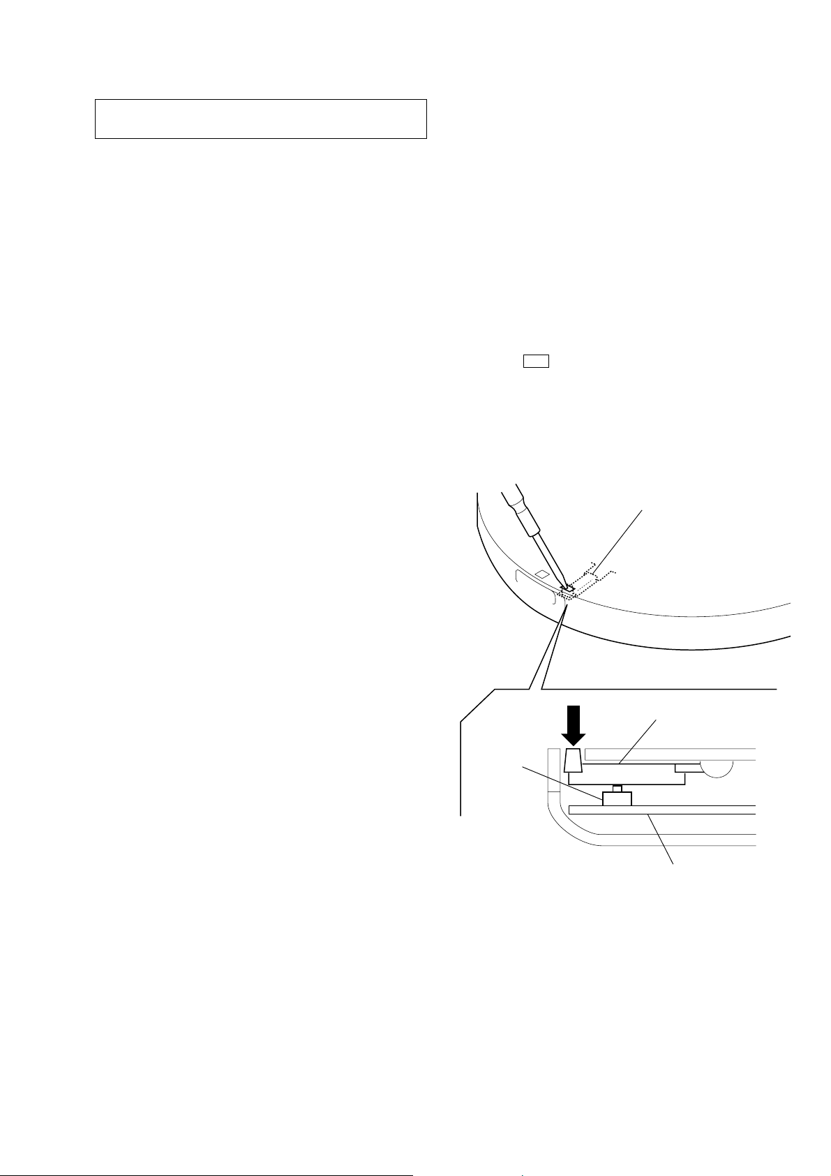
LASER DIODE AND FOCUS SEARCH OPERATION
CHECK
During normal operation of the equipment, emission of the laser
diode is prohibited unless the upper lid is closed while turning ON
the S302. (push switch type)
The following checking method for the laser diode is operable.
• Method:
Emission of the laser diode is visually checked.
1. Open the upper lid.
2. With a disc not set, turn on the S302 with a screwdr iver ha ving a
thin tip as shown in Fig.1.
3. Press the u button.
4. Observing the objective lens, check that the laser diode emits
light.
When the laser diode does not emit light, automatic power control
circuit or optical pickup is faulty.
In this operation, the objective lens will move up and down 4
times along with inward motion for the focus search.
detection lever
detection lever
S302
Fig. 1 Method to push the S302
MAIN board
3
Page 4
XP-ER800/ER800N/ER800R
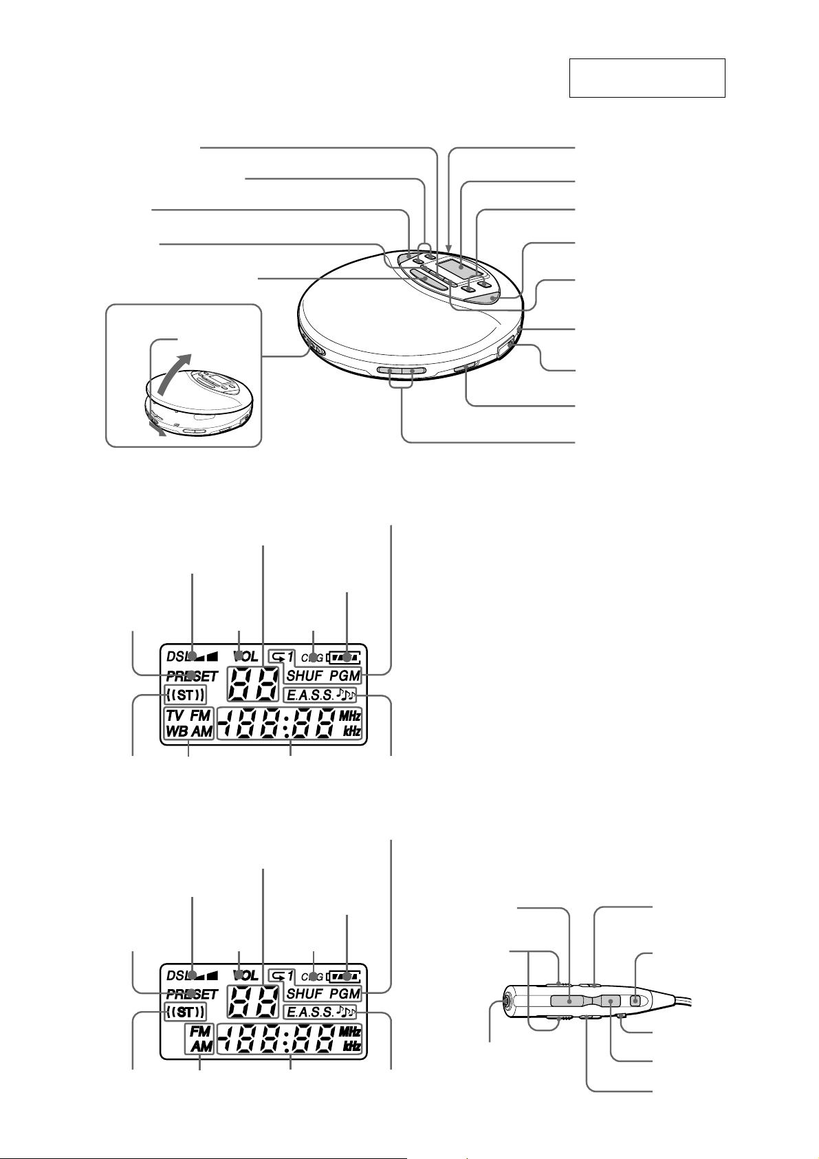
CD player (front)
SECTION 2
GENERAL
This section is extracted
from instruction manual.
1ENTER/DISPLAY
2PRESET CALL UP/DOWN
3BAND
4SOUND
567 s(stop)/OFF/CHARGE
A
*The button has a tactile dot.
Display on CD player
(4 Band)
OPEN
Track number/PRESET number
Strap holes
Display
8r/t
SKIP/SEARCH
9ca*
0MODE
DC IN 4.5 V
(external power
input) jack
\ (headphones)
jack
!HOLD
@VOL +*/–
Play mode
(2 Band)
PRESET
PRESET
Sound mode
VOL CHG
BandST
Track number/PRESET number
Sound mode
Playing time/
Frequency
VOL CHG
Remaining
battery power
Remaining
battery power
E•A•S•S
Play mode
Remote control (XP-ER800R only)Display on CD player
9ca 8tF SKIP
@VOL
3BAND
!HOLD
Earphones jack
BandST
Playing time/
Frequency
E•A•S•S
56s
8rB SKIP
4
Page 5
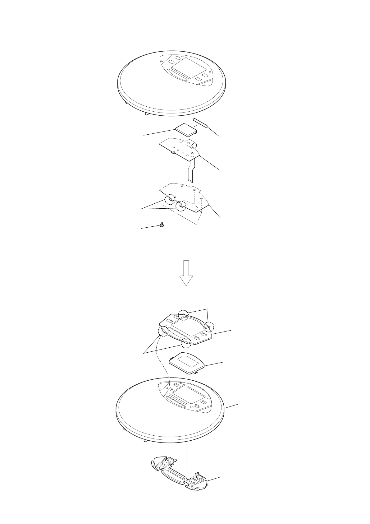
DISASSEMBLY
Note : Disassemble the unit in the order as shown below.
SET
XP-ER800/ER800N/ER800R
SECTION 3
CABINET (REAR) SECTION
CD mechanism deck
(CDM-3325ER)
Motor (turn table) assy (M902),
optical pick-up assy
CABINET (FRONT)
SUB SECTION
MAIN BOARD
UPPER LID
5
Page 6

XP-ER800/ER800N/ER800R
Note : Follow the disassembly procedure in the numerical order given.
3-1. Cabinet (Rear) Section
3
six screws (B2)
2
two screws (B2)
1
Open the battery lid.
5
Remove the cabinet (front) assy,
upper lid assy in the direction of
the arrow.
7
switch unit assy (28P)
(CN301)
6
hold knob
8
remove the
soldering
4
claw
9
cabinet (rear) assy
6
Page 7

3-2. Cabinet (Front) Sub Section
1
Remove the full open left spring in
the direction of the arrow.
2
full open left spring
4
full open right spring
XP-ER800/ER800N/ER800R
3
Remove the full open right spring in
the direction of the arrow.
upper cabinet
upper cabinet
upper cabinet
6
Remove the upper lid assy in
the direction of the arrow.
5
two claws
7
cabinet (front) sub assy
7
Page 8
XP-ER800/ER800N/ER800R
l
3-3. Upper Lid
5
liquid crystal display panel
6
LCD rubber
4
switch unit assy
2
two claws
1
seven screws
8
two claws
3
lid cover
9
two claws
0
display pane
qa
display window
qs
upper lid
7
control button
8
Page 9
3-4. CD Mechanism Deck (CDM-3325ER)
P)
4
three insulators
3
flexible board
(15P) (CN501)
XP-ER800/ER800N/ER800R
5
CD mechanism deck
(CDM-3325ER )
1
connector (2P)
(CN202)
2
connector (4
(CN201)
9
Page 10
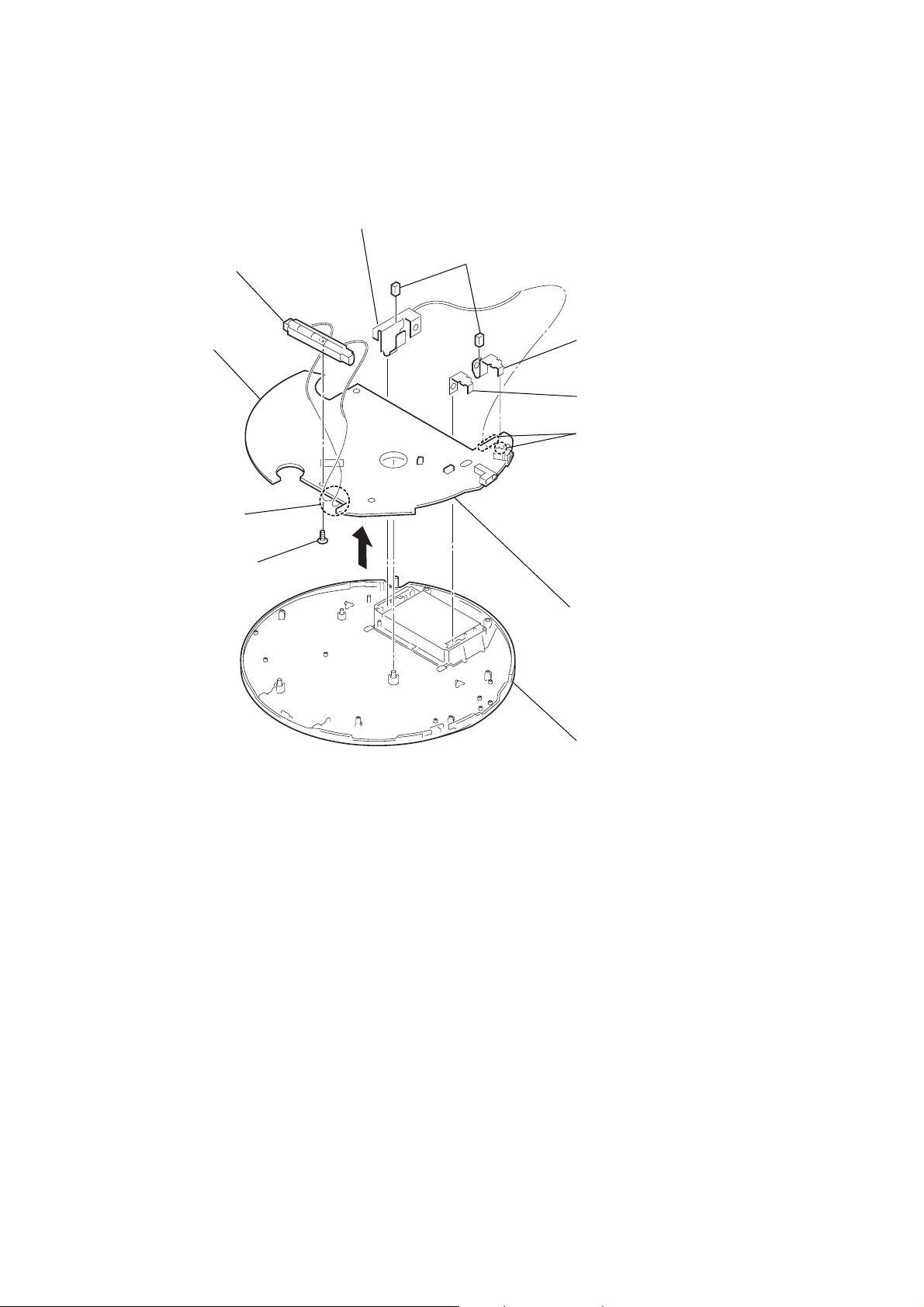
XP-ER800/ER800N/ER800R
3-5. MAIN Board
9
bar-ant holder
qa
MAIN board
6
battery terminal board (relay)
1
two comtact cushions
4
battery terminal
−
board (
5
battery terminal
board (
3
Remove soldering from
the three points.
)
+
)
7
Remove soldering
from the two points.
8
tapping screw
(B1.7 )
2
Remove the MAIN board
in the direction of the arrow.
0
lower cabinet
10
Page 11
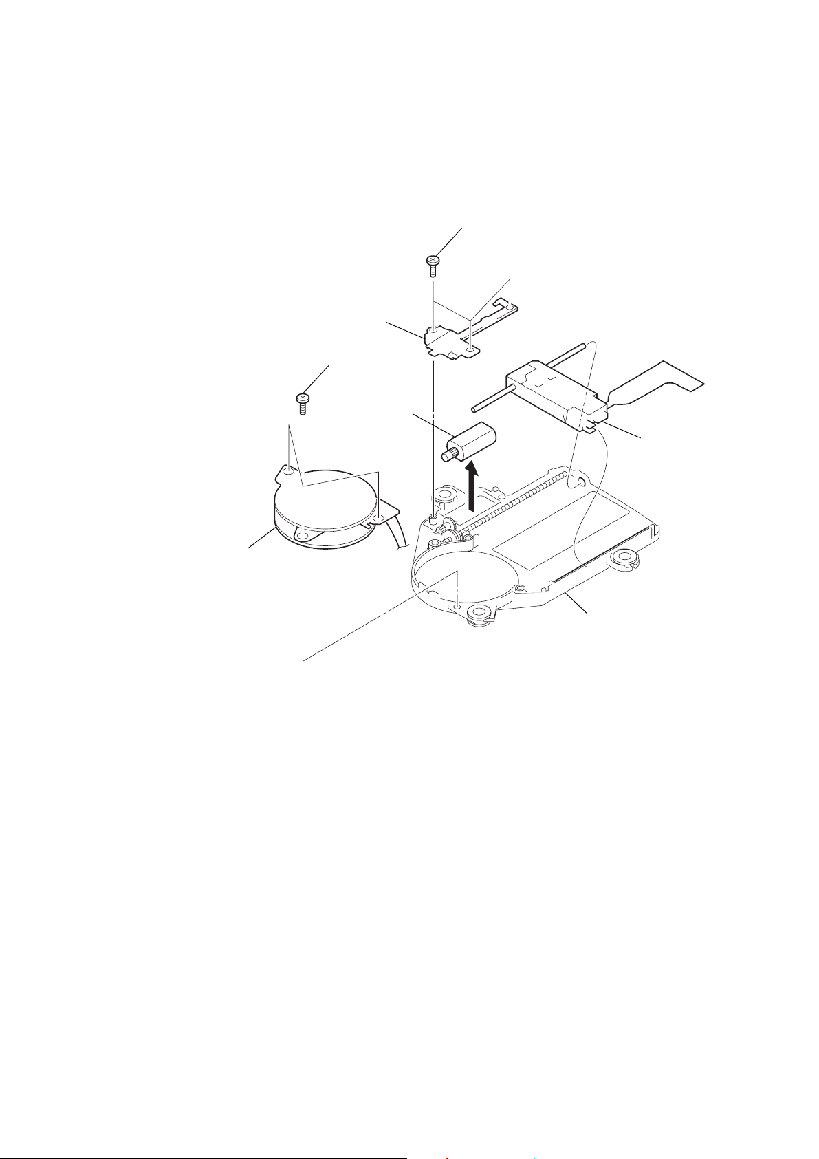
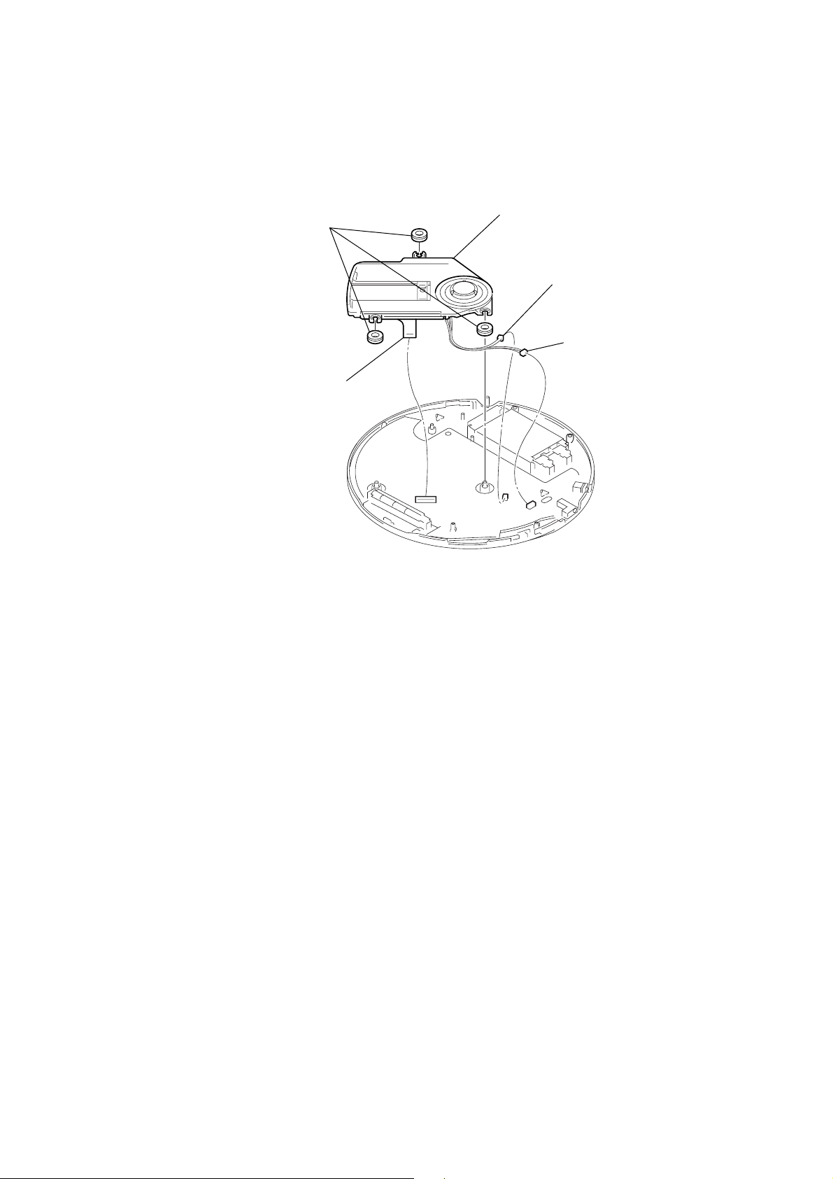
3-6. Motor (Turn Table) Assy (M902), Optical Pick-Up Assy
1
(B1.7x4)
2
gear cover
5
three screws
(B1.7x4)
3
motor assy
(sled) (M901)
three screws
XP-ER800/ER800N/ER800R
4
optical pick-up
(DAX-25E)
6
motor (Turn table )
assy (M902)
chassis
11
Page 12
XP-ER800/ER800N/ER800R
)
)
SECTION 4
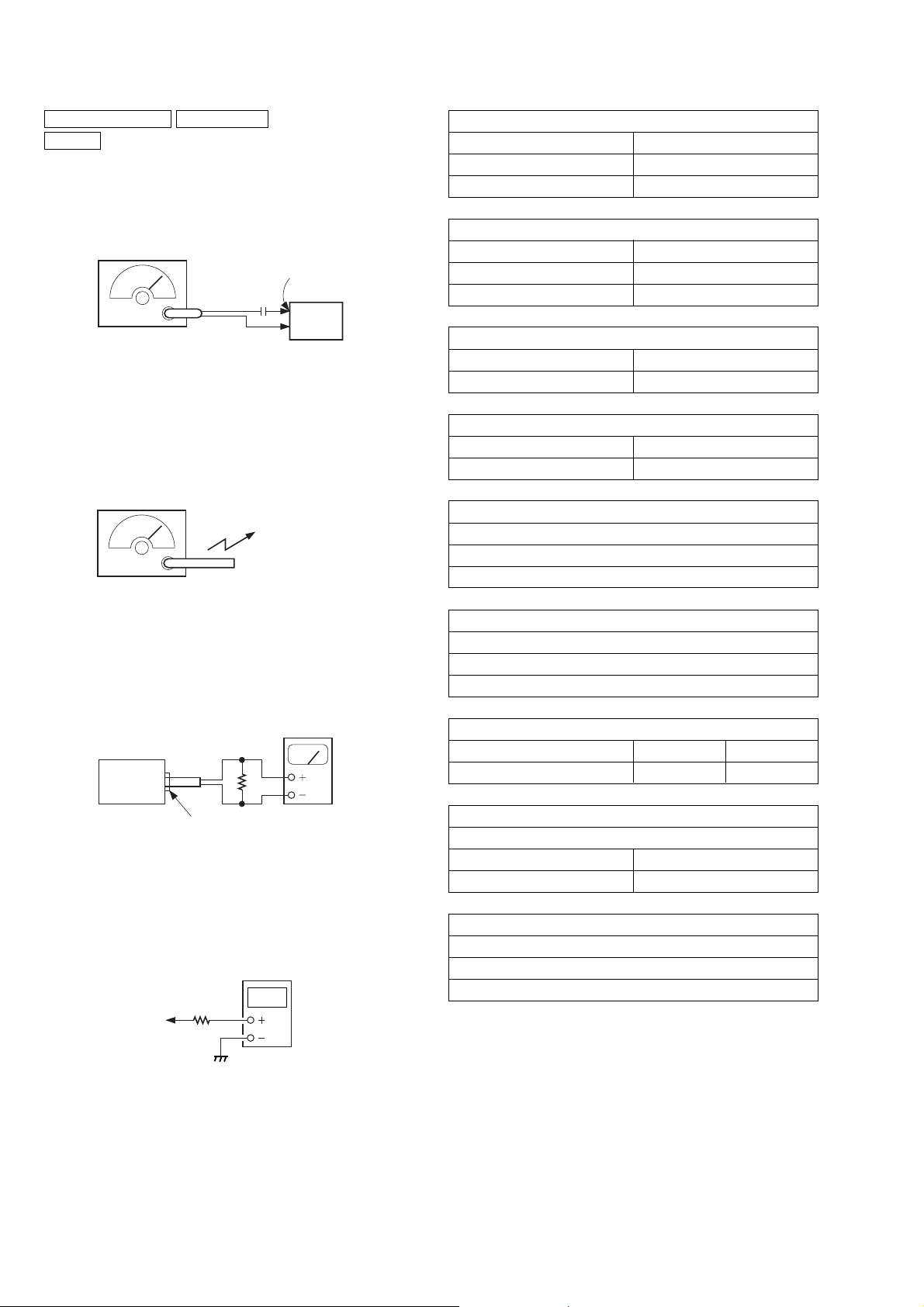
ELECTRICAL ADJUSTMENT
TUNER SECTION 0 dB = 1 µV
4 band
• FM Section (TRACKING ADJUSTMENT)
Setting :
BAND : FM, WB
FM RF signal
generator
TP901 (RF-IN
0.01
µ
F
set
75kHz frequency
deviation by 1kHz signal
output level : as low as possible
• AM Section (TRACKING/IF ADJUSTMENT)
Setting :
BAND : AM
AM RF signal
generator
30% amplitude
modulation by
1kHz signal
Put the lead-wire
antenna close to
the set.
• Connecting Level Meter (FM and AM)
TV VT ADJUSTMENT
Frequency display
Reading on digital voltmeter
Adjustment part
FM VT ADJUSTMENT
Frequency display
Reading on digital voltmeter
Adjustment part
WB VT CHECK
Frequency display
Reading on digital voltmeter
TV VT CHECK
Frequency display
Reading on digital voltmeter
WB TRACKING ADJUSTMENT
Adjust for a maximum reading on level meter
L904
WB 1ch
FM TRACKING ADJUSTMENT
Adjust for a maximum reading on level meter
L902
87.5 MHz
TV 13ch (215.75MHz)
9.0 ± 0.3V
L903
108MHz
10.0 ± 0.3V
L901
WB 2ch (162.400MHz)
5.4 ± 0.5V
TV 2ch (59.75MHz)
0.7 ± 0.5V
level meter
(range: 0.5–5 V ac
16
Ω
set
i
jack (J702)
• Connecting Digital Voltmeter
(FM/TV/WB/AM VT ADJUSTMENT or CHECK)
digital
voltmeter
Ω
100 k
TP903 (VT)
Repeat the procedures in each adjustment several times.
Adjustment and Check Location : MAIN Board (see page 13)
AM VT CHECK
Frequency display
Reading on digital voltmeter
AM TRACKING ADJUSTMENT
Adjust for a maximum reading on level meter
L801
600kHz
AM IF ADJUSTMENT
Adjust for a maximum reading on level meter
1.0 ± 0.5V
T901
1,000kHz
530kHz
1710kHz
7.0 ± 1V
CT801
1,400kHz
12
Page 13
Adjustment and Check Location :
— MAIN Board (Side A) —
L901
CT801
T901
XP-ER800/ER800N/ER800R
L901
FM VT
adjustment
L903
TV VT
L902
L903
L904
adjustment
L902
FM TRACKING
adjustment
L904
WB TRACKING
adjustment
@
@
@
— MAIN Board (Side B) —
IC201
L801
L801,CT801
AM TRACKING
adjustment
IC304
L901
AM IF
adjustment
4band
IC451
IC401
IC902
IC901
IC501
TP903 (VT)TP901 (RF-IN)
4band
13
Page 14
XP-ER800/ER800N/ER800R
)
2 band
• FM Section (TRACKING ADJUSTMENT)
Setting :
BAND : FM
FM RF signal
generator
TP851 (RF-IN
µ
F
0.01
set
75kHz frequency
deviation by 1kHz signal
output level : as low as possible
• AM Section (TRACKING/IF ADJUSTMENT)
Setting :
BAND : AM
AM RF signal
generator
30% amplitude
modulation by
1kHz signal
Put the lead-wire
antenna close to
the set.
• Connecting Level Meter (FM and AM)
level meter
(range: 0.5–5 V ac)
Ω
16
FM VT ADJUSTMENT
Frequency display
Reading on digital voltmeter
Adjustment part
FM VT CHECK
Frequency display
Reading on digital voltmeter
FM TRACKING ADJUSTMENT
Adjust for a maximum reading on level meter
L852
108MHz
AM VT CHECK
Frequency display
Reading on digital voltmeter
AM TRACKING ADJUSTMENT
Adjust for a maximum reading on level meter
L801
603kHz
AM IF ADJUSTMENT
Adjust for a maximum reading on level meter
1.0 ± 0.5V
T851
999kHz
531kHz
108MHz
8.0 ± 0.3V
L853
87.5MHz
1.5 ± 1.0V
1602kHz
6.5 ± 1V
CT801
1,404kHz
set
i
jack (J702)(EXCEPT AEP,HK)
(J701)(AEP,HK)
• Connecting Digital Voltmeter
(FM/TV/WB/AM VT ADJUSTMENT or CHECK)
digital
voltmeter
Ω
100 k
TP854 (VT)
Repeat the procedures in each adjustment several times.
Adjustment and Check Location : MAIN Board (see page 15)
14
Page 15
@
Adjustment and Check Location :
— MAIN Board (Side A) —
XP-ER800/ER800N/ER800R
L853
FM VT
adjustment
— MAIN Board (Side B) —
T851
AM IF
adjustment
@
L801
T851
L801,CT801
AM TRACKING
adjustment
L853
CT801
L852
L852
FM TRACKING
adjustment
@
2band
TP854
(VT)
TP851
(RF-IN)
IC201
IC851
IC304
IC501
IC451
IC401
2band
15
Page 16

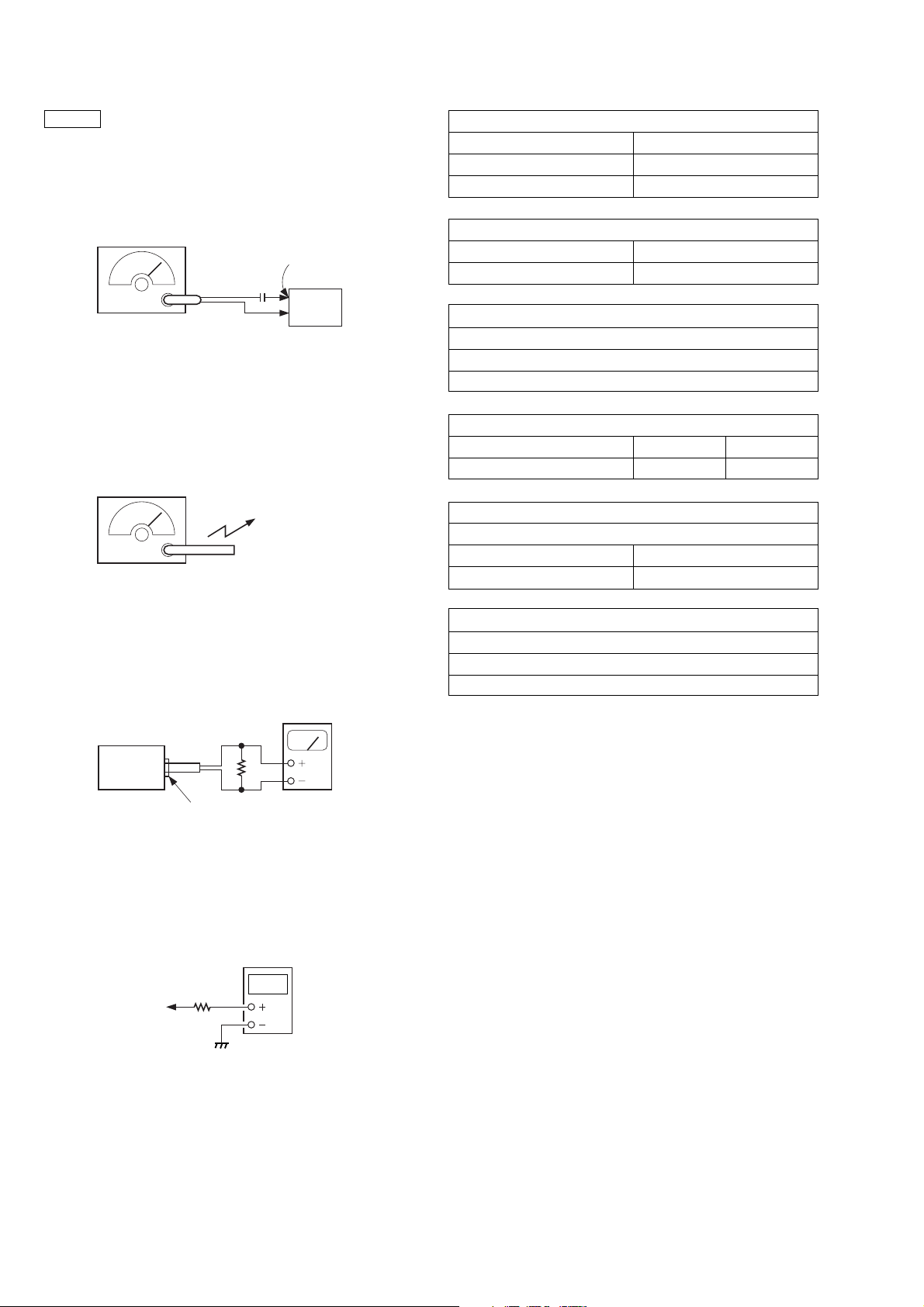
XP-ER800/ER800N/ER800R
K
CD SECTION
The CD section adjustments are done automatically in this set.
In case of operation check, confirm that focus bias.
PRECAUTIONS FOR CHECK
1. Perform adjustment in the order given.
2. Use YEDS-18 disc (Part No.: 3-702-101-01) unless otherwise
indicated.
3. Power supply voltage requirement: DC4.5 V in DC IN jack.
(J101)
VOLUME : Minimum
[HOLD] switch : OFF
FOCUS BIAS CHECK
Condition:
• Hold the set in horizontal state.
Connection:
oscilloscope
(AC range)
MAIN board
TP507 (RF)
TP104 (GND)
2 k
Ω
+
–
Procedure:
1. Connect the oscilloscope to the test points TP507 (RF) and TP104
(GND) on the MAIN board.
2. Set a disc. (YEDS-18)
3. Press the B X key on the set.
4. Check the oscilloscope waveform is as shown below.
A good eye pattern means that the diamond shape (◊) in the
center of the waveform can be clearly distinguished.
RF Signal reference Waveform (Eye Pattern)
VOLT/DIV : 100 mV (With the 10:1 probe in use)
TIME/DIV : 500 ns
RF level
0.9 ± 0.1 Vp-p
To watch the eye pattern, set the oscilloscope to AC range and
increase the vertical sensitivity of the oscilloscope for easy watching.
5. Stop revolving of the disc motor by pressing the
OFF/CHARGE x key on the set.
Connecting and Checking Location:
– MAIN Board (Side B) –
TP104
(GND)
IC201
IC304
FOCUS BIAS CHEC
16
IC902
IC901
TP507
(RF)
IC501
IC451
IC401
Page 17

SECTION 5
DIAGRAMS
NOTE FOR PRINTED WIRING BOARDS AND SCHEMATIC DIAGRAMS • WAVEFORMS
XP-ER800/ER800N/ER800R
Ver 1.1 2003.06
Note on Printed Wiring Board
• X : parts extracted from the component side.
• Y : parts extracted from the conductor side.
• : Pattern from the side which enables seeing.
(The other layers' patterns are not indicated.)
Caution:
Pattern face side: Parts on the pattern f ace side seen from
(Side B) the pattern face are indicated.
Parts face side: Parts on the parts face side seen from
(Side A) the parts face are indicated.
Note on Schematic Diagram:
• All capacitors are in µF unless otherwise noted. pF: µµF 50 WV or
less are not indicated except for electrolytics and tantalums.
• All resistors are in Ω and 1/
•%: indicates tolerance.
f
•
• C : panel designation.
• H : adjustment for repair.
• A : B+ Line.
•Total current is measured with CD installed.
•Power voltage is DC 4.5 V and f ed with regulated dc po w er supply
•Voltages and waveforms are DC with respect to ground in playback
•Voltages are taken with a VOM (Input impedance 10 MΩ).
•Waveforms are taken with a oscilloscope.
• Circled numbers refer to waveforms.
• Signal path.
: internal component.
Note:
The components identified by mark 0 or dotted
line with mark 0 are critical for safety.
Replace only with part
number specified.
from DC IN jack (J101).
mode.
no mark : CD PLAY
Voltage variations may be noted due to normal production toler-
ances.
Voltage variations may be noted due to normal production toler-
ances.
J : CD PLAY
K : FM
e : AM
4
W or less unless otherwise specified.
Note:
Les composants identifiés par
une marque 0 sont critiques
pour la sécurité.
Ne les remplacer que par une
piéce portant le numéro
spécifié.
1
IC501 9 ARF
200mV/DIV, 400ns/DIV
800 mVp-p
4
IC201 ef SYNC
176.4kHz
1V/DIV, 2µs/DIV
5.7 µs
7
Q804 collector
2.4 Vp-p
1V/DIV, 100ns/DIV
3.8 Vp-p
334 ns
2
IC401 uh X2
1V/DIV, 20ns/DIV
2.8 Vp-p
59ns
5
IC304 0 OSC2
1V/DIV, 100ns/DIV
236ns
8
IC851 w; XOUT
2.0 Vp-p
500mV/DIV, 4µs/DIV
1.3 Vp-p
13.3 µs
3
IC401 ya MCLK
1V/DIV, 400ns/DIV
945ns
6
IC901 w; XOUT
2.3 Vp-p
500mV/DIV, 4µs/DIV
910mVp-p
13.3 µs
9
Q804 collector
1V/DIV, 100ns/DIV
3.9 Vp-p
337ns
1717
Page 18

XP-ER800/ER800N/ER800R
Ver 1.1 2003.06
5-1. Block Diagram – Main Section –
OPTICAL PICK-UP
BLOCK
VCC
RF
A
B
E
F
LD
GND
PD
VR
PU STBY
TRACKING
COIL
FOCUS
C0IL
SLED
M
MOTOR
SPINDLE
MOTOR
GAIN UP
IC501
RF AMP
VCC3
RF IN
6
32
PDA
PDB
30
PDE
27
PDF
28
Q502
APC
Q503
T+
T-
F-
F+
S+
S-
LD
2
LPD
1
MOTOR/COIL DRIVE
FO2
48
RO2
46
FO3
44
RO3
42
FO1
52
RO1
50
SPCOM
80
SPUIN
79
U-OUT
2
SPVIN
78
V-OUT
4
SPWIN
77
W-OUT
6
VCC
ARF
FEOUT
TEOUT
3TOUT
RFDET
OFTR
BDO
GCTL
PDOWM
IC201(1/2)
F2
R2
F3
R3
F1
R1
BRK
PWM
XRST
DATA
CLOCK
LATCH
RST_OUT
SYNC 176.4kHz
WAKEUP
FG
VCC3
3
9
23
21
11
16
25FBAL
26TBAL
15
13
24
18
58
57
60
59
56
55
70
72
36
39
38
40
35
34
37
74
Q401
X401
16.93MHz
39
43
42
32
33
34
36
31
30
35
37
38
25
26
27
28
23
24
70
77
76
80
22
IC401
DSP + EASS DECODER
ARF
DRF
DSLF
FE
TE
RFENV
NRFDET
FBAL
TBAL
OFT
BDO
LDON
TRP
TRM
FOP
FOM
TRVP
TRVM
SPPOL
X1
X2
EXT2
SPOUT
IOVDD2
ADPVCC
OUTL
OUTR
EXT1
AVDD1
AVDD2
DRVDD
DVDD2
IOVDD1
A10
NWE
NRAS
NCAS0
MDTA
MCLK
MLD
NDRST
BLKCK
Q705
TU MUTE
SWITCH
48
IC451
16M DRAM
A0
A10
XWE
XRAS
XCAS
D0
D3
Q706,707
B+
SWITCH
Q703,704
B+
SWITCH
T-ON
2
.
3
.
24
.
25
VCC3
58
51
VCC3
46
1
59
79DVDD1
21
29
41
2
.
D0
3
.
6
D3
.
7
16
19
.
14
A0
10
.
15
.
9
4
5
8
62
61
63
69
68STAT
64
VCC1
VCC2
V MON
BATT
9
12
.
15
19
.
21
.
8
4
5
23
X301
4.19MHz
Q304
MDT
MCK
MLEN
MDT
MCK
MLEN
6
11
7
16
15
14
51
50
49
10
11
8
29
31
58
35
30
43
39
38
32
34
33
17
36
37
40
IC702
VOLUME
LIN
RIN
AVDD
MDT
MCK
MLEN
MDT
MCK
MLEN
OSC2
OSC1
CLK-SHT
MDATA
MCLK
XMLD
NRST
STAT
BLKCK
SP
XPUON
S/P-DATA
S/P-CLK
S/P-LAT
RST
SYNC
WU
FG
5
LOUT
12
ROUT
Q708,709
BEEP
T-ON
PLL-CE
T-DI
T-DO
T-CLK
EEP-CE
HOLD
VOLUME
DOOR
VDD
VDD
VDIN
AC-IN
SWITCH
27
46 STANDBY
48MUTE
52
54
56
55
57
53
80-77COM01-04
76-59SEG01-18
20K-FUNC1
21K-FUNC2
19K-P/S/B
42WAKEUP
22K-RMC
45
26
41
16
44
25
23
24
B+
AEP,HK
4DVDD VCPU
IC304
µCOM
CHGMNT
T-ON
TU-CE
TU-DI
TU-DO
TU-CLK
Q701
BST
SWITCH
Q302
WAKEUP
SWITCH
S303, 304
VOLUME
KEY
BATT
Q702
BIAS
IC302
EEPROM
6
DO
5
DI
4
SK
3
CS
S301
HOLD.
OFF
ON
S302
(OPEN/CLOSE)
15
1450
17
20
19
236DSL1
Q301
17DSL2
IC701
HP AMP
IN-L
IN-R
BEEP
PWSW
MUTSW
BSTSW
BSTN
LCD1
LIQUID
CRYSTAL
DISPLAY
FUNCTION
KEY
VCC
US, CND, AUS, ER800:E13
L
6
8R
5
BATT
VCPU
AEP, UK, HK, TW, ER800R:E13
TU-VCC
TU-VDD
IC201(2/2)
POWER CONTROL
VMON
VCC1
(2.25V)
VCC2
(2.0V)
VCC3
(2.65V)
TU-VDD
VCPU
(2.0V)
66
17
10
18
11
19
67
VMMNT
VCC1
SSW
VCC2
VCC3
VCPU
CHGMNT
LG
VIN
DCIN_S
SPVCC
SPVCC
VM1
VM12
VM23
VM3
BATM1
BATM2
VCC
VCC0
STNG
REGB
DCIN
CHGB
DET
L-CH
R-CH
FM-ANT
TU-VCC
TU-VDD
(4BAND) MUTE
T-ON
TU-DI
TU-DO
TU-CLK
TU-CE
8
12
64
1
5
53
49
45
41
68
69
20
16
25
62
61
65
63
Q101
CHARGE
SWITCH
A
A
J702
i
C
C
J701
i
/(REMOTE)
B
B
TU-VCC
BATT
Q202
REG
D202
TUNER(2BAND)
SECTION
TUNER(4BAND)
SECTION
TUNER(2BAND)
SECTION
TUNER(4BAND)
SECTION
TUNER(2BAND)
SECTION
TUNER(4BAND)
SECTION
Q203
Q201
D203
D103
• Signal Path
: CD
: FM(2BAND)
: FM, TV, WB(4BAND)
: AM
(IEC DESIGNATION LR6)
DRY BATTERY
SIZE "AA"
2PCS, 3V
RECHARGEABLE
BATTERY
SIZE "AA"
Ni-MH, 700mAh
2PCS, 2.4V
J101
DC IN 4.5V
1818
Page 19

5-2. Block Diagram – TUNER (4Band) Section –
L902
FM
TRACKING
L904
WB
TRACKING
L901
FM VT
L903
TV VT
L801, CT801
AM
TRACKING
Q903
Q905
TU-VCC
L802
D902
TU-VCC
D801
CT801
Q901
L902
L904
Q904, 906
FERRITE-ROD
ANTENNA
L801
D901
TU-VCC
Q801
RF AMP
L901
L903
IC902
FRONT-END
IF AMP,DET,FM MPX
FM IN
2
FM RF
24
FM OSC
21
AM RF
22
AM OSC
20
FM
MIX
FM
OSC
AM
MIX
AM
OSC
MIX OUT
OSC OUT
XP-ER800/ER800N/ER800R
• Signal Path
: FM, TV, WB
: AM
TU-VCC
CF903
10.7MHz
10
QUAD
CF902
10.7MHz
4
T901
CF901
450kHz
T901
AM IF
TU-VDD
Q902
BUFFER
19
X903
75kHz
IC901
PLL
VDD
13
FM IN
12
11
20
19
AM IN
XOUT
XIN
XST/MO
XST
XAM
IF IN
FM IF IN
7
AM IF IN
6
BUFFER
LPF1
ST LED
LPF2
14
18
13
6
9
5
10
IF
17
IF REQ
FM
DET
AM
DET
REQ
IF
23 5
RF VCC VCC
FM/AM
BUFFER
Q908
DET OUT
MPX-IN
TU-VCC
FM
MPX
16
15
MUTE
L-OUT
R-OUT
Q802
SWITCH
12
11
B+
Q803
TU-VDD
(2V)
L-CH
R-CH
TU-VCC
T-ON
TU-VDD
MUTE
A
B
MAIN
SECTION
MAIN
SECTION
D903
D904
Q907
BAND
SWITCH
Q909
BAND
SWITCH
FL901
BAND
PASS
FILTER
TU-VCC
Q804, T801,
D802, 803
DC/DC CONVERTER
AOUT
17
AIN
16
PD
15
8 XTV/WT
7 TV/WT
DO
4
DI
2
CL
3
CE
1
TU-DI
TU-DO
TU-CLK
TU-CE
FM-ANT
C
MAIN
SECTION
1919
Page 20

XP-ER800/ER800N/ER800R
5-3. Block Diagram – TUNER (2Band) Section –
FL851
BAND
PASS
FILTER
L852
FM
TRACKING
L853
FM VT
TU-VCC
L852
D851
D852
TU-VCC
L853
IC851 (1/2)
FRONT-END
IF AMP,DET,FM MPX
FMIN
36
FMRF
34
FM
OSC
32
FM
MIX
FM
OSC
FMMIX
AMMIX
• Signal Path
: FM
: AM
TU-VCC
CF853
10.7MHz
11
FM
DET
CF851
10.7MHz
2
T851
4
T851
AM IF
CF852
450kHz
FMIF
6
AMIF
7
IF
BUFFER
TO
PLL
DET
AM
DET
FM
FM
DETO
AM
DETO
33 8
RF VCC VCC
27
26
25
MPXIN
MUTE
FM
MPX
LCH
RCH
12
13
L-CH
R-CH
A
MAIN
SECTION
L801, CT801
AM
TRACKING
TU-VCC
L802
D801
CT801
L801
FERRITE-ROD
ANTENNA
Q801
RF AMP
AMRF
1
AM
OSC
31
TU-VCC
AM
MIX
AM
OSC
Q804, T801,
D802, 803
DC/DC CONVERTER
TO
PLL
X852
75kHz
TU-VDD
21
20
19
24
23
22
IC851 (2/2)
VDD
XOUT
XIN
AOUT
AIN
PD
PLL
DO
18
DI
16
CL
17
CE
15
TU-VCC
TU-VDD
(2V)
Q802
B+
SWITCH
Q805
B+
SWITCH
Q803
Q806
TU-VCC
T-ON
TU-VDD
TU-DI
TU-DO
TU-CLK
TU-CE
FM-ANT
B
C
MAIN
SECTION
MAIN
SECTION
2020
Page 21

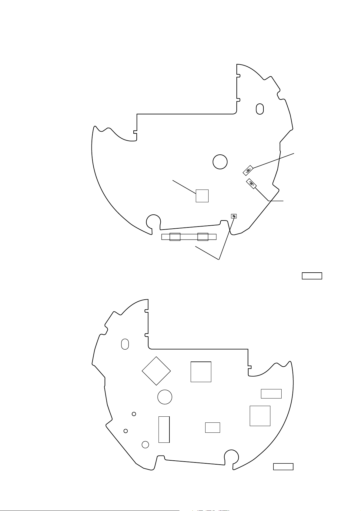
5-4. Printed Wiring Board – MAIN Board (4Band US, CND Only)(Side A) –
XP-ER800/ER800N/ER800R
Ver 1.1 2003.06
12
MAIN BOARD
(SIDE A)
3456789
A
D101
DRY BATTERY
SIZE "AA"
(IEC DESIGNATION LR 6)
2PCS,3V
RECHARGEABLE
M901
(SLED MOTOR)
M902
(SPINDLE MOTOR)
SWITCH UNIT,
LCD1
BATTERY
SIZE "AA"
Ni-MH, 700mAh
2PCS, 2.4V
B
2
C
28
27
E
D
E
OPTICAL PICK-UP
BLOCK
DAX-25E
C807
R817
E
S
S
E
E
E
C
B
1
C738
J702
i
• Semiconductor
R710
Location
Ref. No. Location
D101 A-6
D102 B-6
D103 A-6
D203 B-6
D903 E-6
ON
S301
OFF
HOLD
D904 E-6
IC701 D-6
Q101 A-6
Q201 B-6
IC701
S
Q203 C-6
Q502 F-4
Q701 D-6
Q802 E-4
Q803 E-4
Q902 E-6
Q907 E-6
Q908 E-5
S303
VOL
S
S
Q909 E-6
11
VOL
(11)
S304
C524
E
1-688-136-
F
S302
(OPEN/CLOSE)
2121
Page 22

XP-ER800/ER800N/ER800R
Ver 1.1 2003.06
5-5. Printed Wiring Board – MAIN Board (4Band US, CND Only)(Side B) –
12
MAIN BOARD
(SIDE B)
3456789
A
J101
4.5
C108
B
C112
(GND)
• Semiconductor
Location
Ref. No. Location
C215
S
C320
C
E
IC201
E
D
C739
R719
E
E
S
E
E
S
IC702
IC304
E
IC302
C822
E
R349
S
E
E
S
E
S
R751
IC451
IC401
S
E
(RF)
IC901
E
(RF-IN)
E
IC902
S
S
X903
IC501
(VT)
(VT)
S
1-688-136-
11
(11)
D202 C-4
D801 F-4
D802 C-6
D803 C-6
D901 D-3
D902 E-2
IC201 C-3
IC302 C-5
IC304 C-5
IC401 D-6
IC451 D-6
IC501 E-5
IC702 D-4
IC901 E-4
IC902 E-3
Q202 C-4
Q301 D-5
Q302 D-5
Q304 C-4
Q401 D-7
Q503 F-5
Q702 D-2
Q703 D-5
Q704 D-5
Q705 E-5
Q706 D-5
Q707 D-5
Q708 D-4
Q709 D-4
Q801 F-4
Q804 C-6
Q901 E-3
Q903 E-2
Q904 E-3
Q905 E-3
Q906 E-3
F
L801
BAR-ANTENNA
2222
Page 23

5-6. Printed Wiring Board – MAIN Board (2Band Except US, CND)(Side A) –
XP-ER800/ER800N/ER800R
Ver 1.1 2003.06
12
MAIN BOARD
(SIDE A)
3456789
A
DRY BATTERY
SIZE "AA"
(IEC DESIGNATION LR 6)
2PCS,3V
RECHARGEABLE
M901
(SLED MOTOR)
M902
(SPINDLE MOTOR)
SWITCH UNIT,
LCD1
BATTERY
SIZE "AA"
Ni-MH, 700mAh
2PCS, 2.4V
B
2
E
E
C
C
AEP,HK
B
AEP,HK
1
AEP, UK, HK, TW, ER800R:E13
J701
i
AUS, ER800:E13
J702
i
C
28
27
AEP
E
ON
S301
OFF
D
HOLD
• Semiconductor
Location
Ref. No. Location
D101 A-6
IC701
S
D102 B-6
D103 A-6
D203 B-6
D801 E-6
IC701 D-6
C869
E
OPTICAL PICK-UP
BLOCK
DAX-25E
C870
C823
VOL
S303
Q101 A-6
Q201 B-6
Q203 C-6
Q502 F-4
Q701 E-6
Q801 F-6
11
VOL
(11)
S304
E
S
1-688-137-
F
S302
(OPEN/CLOSE)
2323
Page 24

XP-ER800/ER800N/ER800R
Ver 1.1 2003.06
5-7. Printed Wiring Board – MAIN Board (2Band EXCEPT US, CND)(Side B) –
12
MAIN BOARD
(SIDE B)
3456789
A
J101
4.5
(GND)
B
• Semiconductor
Location
Ref. No. Location
D202 C-4
S
C
E
R357
IC304
IC302
IC201
AEP
E
IC451
E
D
R748
C739
R719
E
E
(VT)
IC851
E
(RF-IN)
IC702
S
E
S
S
E
E
E
S
S
IC401
E
E
(RF)
S
IC501
S
1-688-137-
11
(11)
D802 C-6
D803 C-6
D851 E-2
D852 E-3
IC201 C-3
IC302 C-5
IC304 C-5
IC401 D-6
IC451 D-6
IC501 E-5
IC702 D-4
IC851 E-3
Q202 C-4
Q301 D-5
Q302 D-5
Q304 C-4
Q401 D-7
Q503 F-5
Q702 D-2
Q703 D-5
Q704 D-5
Q705 E-5
Q706 D-5
Q707 D-5
Q708 D-4
Q709 D-4
Q802 E-4
Q803 E-4
Q804 C-6
Q805 E-4
Q806 E-4
F
L801
BAR-ANTENNA
2424
Page 25

5-8. Schematic Diagram – MAIN Board (1/6) –
XP-ER800/ER800N/ER800R
Ver 1.1 2003.06
• See page 33 for IC Block Diagrams.
AEP, UK, HK,TW,
ER800R:E13
J701
J702
US, CND, AUS,
ER800:E13
C112
DTC114YUA-T106
IC702
10k
10k
10k
R751
47k
Q707
2SA2018TL
R752
2.2k
Q703
R730
2.2k
Q704
2SA2018TL
SM6451BT-G-E2
C722
C724
1
R731 R732
10k 10k
C723
1
R733
C728
0.01
C729
0.01
Q709
DTC114YUA
-T106 47k
Q705
1
IMX9T110
R745
10
R736
47
22k
R734
0
22k0
R735R746
16V
0.01
0.01
47
730
C732
C
C731
2SA2018TL
Q708
R755
2.2k
22k
R737
6V
1
47
733
C
R740
R741
220k
R738
100k
100k
R742
220k
22k
R739
R757
R707C704
4.7k0.1
1k
708
R758
*
FB701
*
TP701
C735
TP703
TP702
*
L702
FB702
FB703
C701
1000p
TP704
C738
*
L701
*
0.1
TP705
1000p
C702
1000p
C703
R701
R702
0
R748
*
*
10k
703
R
R
C705
220
4V
C706
220 4V
10k
C707 C708
0.1 0.1
R705
4.7
R709
R710
4.7
Q701
DTC114TUA-T106
10 16V
C709
0.1
C711
2.2
C713
C710
0.1
C712
47 4V
R711
2.2
IC701
TA2120FN(EL)
R712
1k
Q702
IMX9T110
C714
100k
R720
R722
47k
0.01
C717
0.22
C716
R747
R714
4.7k
R719
C715
C740
R718
R713
4.7k
R716
R717
10k
R749
1
100k
C718
R715
0.47
100k
100k
R743
2.2E+06pF
100k
10k
47
4V
10k
R725
10k
1k
R723
C719
R724
470k
R721
470k
*
R744
2.2E+06pF
C720
47
4V
C739 1
Q706
DTC114YUA-T106
TP709 TP710
47k
R729
0
1
760
R
C721
R728
R727
R726
US, CND
EXCEPT US,
CND, AEP, HK
R302
R303
R301
R304
470
470
470
470
.1
17400F-10
0
51V
SM
C451
M
C452
IC451
1
R451
10
2525
Page 26

XP-ER800/ER800N/ER800R
5-9. Schematic Diagram – MAIN Board (2/6) –
• See page 17 for Waveforms.
C401
Q401
DTC114TUA-T106
R428
C402
0.1
1
TP401
0
16.93MHz
X401
R406
TP402
R424
TP403
10k
0
TP404
C407
TP410
0.1
0
R429
0
R401
0
R430
0
R427
R425
0
0
R411
0
R412
0.1
C411
TP405
TP407
R423
TP408
TP409
IC401
MN662786SBM
47
0
100k
R420
R421 R413
22k 47k
C403
470
1
C408
470p
R426 R422 R414
4.7k 10k 47k
C406
C418
L401
4.7
100p
R415
R416
C412
6.3V
47
C416
100
R417
0.47
C417
C413
0.1
0.022
C415
0.1
C414
L402
2.2k
R418
0.1
C404
0.1
C423
47 4V
47
0.1
C421
C422
0.01
C420
0
R419
0.1
2626
Page 27

5-10. Schematic Diagram – MAIN Board (3/6) –
XP-ER800/ER800N/ER800R
Ver 1.3 2003.12
• See page 35 for IC Pin Function Descriptions. • See page 17 for Waveforms.
C313
0.01
R318
100k
L302
L304
*
L303
*
Q302
2SA1586YG-TE85L
R306
100k
C305
0.01
TP302
R374R307
R310
470k
Q301
*
R305
*
TP303
TP304
R339
R334
R335
R336
R333
R337
R323
R324
R325
R326
R328
R338
470
470
470
470
470
470
470
470
470
470
470
470
R308
10k
*
C309
*
C307
2.2E+06pF
C310
R315
R372
470k
220k
R316
R373
470k
220k
C308
1000p
C306
1000p
R313
47k
*
S303
47k220k
S304
SL301
0.01
C303
R314
R343
6.3V
22
C301
C319
0.1
R345
470
470
DTC143TUA-T106
TP315
0.1
C315
C316
C317
C318
Q304
1000p
1000p
1000p
C320
10p
47p
C328
R356
IC304
MN101C70C-SA3
0
R357
2.2M
C330
5p
22p
C323
X301
R319
0
4.19MHz
10p
C329
470
R362
C325
0.1
R368 R370 R369 R371
1M 470k 1M 470k
L301
470
0.1
C324
R364
C326 C327
0.1 0.1
TP337
TP338
TP339
TP310
TP312
TP314
TP316
TP317
TP319
TP321
TP322
TP323
TP324
TP326
TP327
TP328
TP329
TP330
TP331
TP332
TP333
TP334
TP335
TP336
TP309
TP340
TP341
TP342
CN301
28PIN
R311
R341
C302
470
R344
470
100
100
100
100
100
470
470
470
470
470
470
470
R367
R366
R363
R365
R361
R359
R360
R358
R355
R352
R349
R347
TP318
R309
S301
220k
0.1
R312
1
0.1
1k
C312
R340
R342
1k
C311
47k
IC302
BR93LL46FV-E2
C304
0.01
100
R351
1k
R354
US, CND
L303 NO MT 10uH 10uH 10uH
L304 NO MT 10uH 10uH 10uH
EXCEPT US,
CND, AEP, HK
TP305
22k
S302
SL302
R320
470k
2727
Page 28

XP-ER800/ER800N/ER800R
5-11. Schematic Diagram – MAIN Board (4/6) –
• See page 32 for IC Block Diagrams. • See page 17 for Waveforms.
TP503
C506
C508
2200p
R509
C507
1000p
100p
47k
R513
R511
R510
VC
0.1
C510
C737
TP520
1
10k
4.7k
10k
C511
6.3V
R520
470k
22
R521
470k
C526
C502
R501
C503
R502
FE
TE
1
0.1
22k
0.1
22k
C505
1000p
R505
TP501
TP502
C509
220p
R506
4.7k
22k
IC501
AN8399SA-E1
TP504
TP519
C512
0.1
C514
C516
TP506
TP530
TP531
C518
C513
C519
C515
C517
TP507
2200p
2200p
1000p
4700p
0.022
0.022
0.1
(RF)
C522
47
16V
Q502
2SB1689-T106
C523
1000p
R527
L502
C524
47 16V
10
C525
0.1
CN501
CN201
4P
R508
4.7k
TP508
TP524
TP525
R503
47k
Q503
DTC114TUA-T106
L501
R516
1
C501
TP516
15P
TP208
TP207
TP205
TP203
TP509
C504
TP510
TP511
TP512
TP513
TP514
TP515
1
R514
10k
R515
4.7k
10k
R517
4.7k
R519
0
TP526
TP527
TP528
TP529
CN202
2P
TP204
TP206
2828
Page 29

XP-ER800/ER800N/ER800R
5-12. Schematic Diagram – MAIN Board (5/6) –
R201
C202
1
C214
L202
C227
R202
C228
L203
C229
R203
0
C230
C232
R204
• See page 32 for IC Block Diagrams. • See page 17 for Waveforms.
C206
1000p
0
0
0
R209
R208
0
2.2
2.2
0
2.2
2.2
2.2
2.2
0
R238
C205
BH6580KV
IC201
0.22
R214
R213
10k
C207
2200p
100k
TP202
R226
L204
Q203
2SB1689
-T106
1k
0
R215
10V
C221
22
16V
C219
47
1
C237
470p
C218
L205
0
C225
L206
1
C233
2.2
C234
2.2
C235
2.2
C231
47
22
4V
C220
C224
10V
C222
1
C223
4V
10V
1
100
C238
10V
C226
22
220
R108
100
TP103
R101
TP101
TP102
100
C104
1
C109
C110
0.1
2SD1781K-T146-Q
D103
MA2H735-(TX).SO
R106
C105
220k
0.1
R105
47k
R107
R109
47k
2.2M
0.1
Q101
0.1
C108
C107
C106
0.01
1
0.01
L102
C111 0.1
BT101
BT102
BT103
BT
BT
C217
220 4V
470
Q202
2SC4116GL-TE85L
D202
MA111-TX
R206
100k
R207
100k
Q201
2SB1237TV2PQR
D203
MA2YD2300LS0
0
R210
1
C208
0.022
C210
0.022
C211
C212
4700p
R224
22k
C213
C215
4700p
4700p
TP209
C203
220
6.3V
R232
R205
0
L210
C236
220 4V
4.7
D101
C101
MA2H735-(TX).SO
1
C102
1
C103
D102
UDZSTE-175.1B
1
R102
2.2
R103
TP104
(GND)
C113 0.1
L101
1
J101
2929
Page 30

XP-ER800/ER800N/ER800R
Ver 1.1 2003.06
5-13. Schematic Diagram – MAIN Board (6A/6)(4Band US, CND Only) –
Q903
DTC114YUA-T106
C909
0.01
0.01
L902
*
C919
2p
L904
*
IC902
TA2149BFN
Q907
DTA114YUA-T106
C910
470k
R906
R908
470
Q905
2SA2018TL
C928
0.01
R917
1k
R928
2.2k
HSC277-TRF
0.01
C933
10
R922
D903
• See page 34 for IC Block Diagrams. • See page 17 for Waveforms.
TP903
(VT)
R902
C903
0.01
D902
47k
R912
HVC300BTRU
220p
C924
1k
Q901
DCT114YUA
-T106
C902
0.01
0
R916
C906
0.01
C907
0.01
*
L901
Q904
2SA2018TL
L903
*
Q906
2SA2018TL
R921
470k
D901
HVC300BTRU
4.7k
2.2k
R911
R910
100p
220p
C921
100p
C923
C922
C905
1000p
Q902
2SC4915-0-TE85L
R907
220
R915
220
C920
0.1
100k
0.01
R920
C934
2.2k
R904
47k
R905
TP909
R909
220
C911
0.01
470
220p
1000p
R919
C930
C931
C935
220p
C936
0.47
TP907
100p
C929
C927 C926
0.1
R918
C932
2.2k
1 0.1
TP913
TP912
C913
22p
X903
75KHz
IC901
LC72122V-TLM
R923
10k
R901
R938
0
47k
C901
2.2
C904
R903
0.01
C912
22p
4.7k
220
R913
C915
0.1
470
100p
100p
C917
R914
C916
TP902
R937
FL901
(RF-IN)
TP901
1000p
0
D904
HSC277-TRF
R932
C950
R936
0
Q909
DTA114YUA-T106
R939
0
C944
100p
R931
2.2k
0.022
C946
0.047
C945
GTVSB3
0
10k
R935
R934
L905
C801
5p
0.1
10p
C820
C804
L802
220p
220p
47p
C806
C805
C823
R802
22k
0.1
C802
L801
BAR-AnT
C803
CT801
D801
SVC347-TL
R804
220
0.1
C807
1000p
TP904
TP914
470
R933
TP905
T901
CF901
PFS450A3
CF902
C937
0.1
C938
4.7
22
6.3V
TP906
C943
0.022
CF903
C939
0.01
C940
R930
220
TP908 TP910
0.01
0.022
C941
C942
R929
220
C947
0.1
C948
0.47
C949
0.47
TP911
Q908
DTC114YUA-T106
1k
1k
1k
1k
R924
R926
R925
R927
C812
1000p
L906
Q802
2SA2018TL
TP801
DTC114TUA-T106
R808
100k
2SC4154TP-1F
Q803
Q804
C824R809C822C821
0.012200.0122
C815 C817
D803
MA111-TX
MA8130-TX
D802
1 0.1
L803
R805
1k
2.2
C813
R806
100k
R807
4.7k
C819
10p
T801
C816
10p
10V
R801
47
Q801
2SK360E-TL
US, CND
3030
Page 31

5-14. Schematic Diagram – MAIN Board (6B/6)(2 Band Except US, CND) –
XP-ER800/ER800N/ER800R
Ver 1.1 2003.06
• See page 17 for Waveforms.
EXCEPT US, CND, AEP, HK
C801
0.1
C820
C805
220p
5p
C804
L802
10p
C806 C823
220p 47p
L851
R882
R851
R875
2SA2018TL
0
Q805
R810
100k
R813
4.7k
Q806
DTC114TUA-T106
TP802
1000p
C812
2SA2018TL
C815
1
MA111-TX
MA8130-TX
D802
Q802
D803
C817
L803
2.2
C813
R806
100k
R807
4.7k
TP801
0.1
Q803
DTC114YUA-T106
R808
100k
C819
R805
1k
10p
C816
T801
10p
Q804
2SC4154TP-1F
10V
0.01
C824
C822
220
R809
0.01
22
C821
TP803
C827
TP854
(VT)
R853
10k
0.01
C853
R852
0
C851
1000p
TP851
(RF-IN)
0
0
D851
FL851
0.01
C854
HVC202A-TRU
*3
L852
R857
8p
C855
10
47k
R859
1000p
C856
C858
470p
C862
4.7k
R860
0.01
R862
R861
10
1k
D852
HVC202A-TRU
*3
10p
L853
C863
0.01
0.01
C866
2.2k
R863
C865
R864
47k
C868
R873
47k
2.2
470p
C861
C825
220p
0.01
4.7
TP857
C873
1
C871
TP858
R867
C878
0.1
4.7k
C879
0
22p
R874
C882
22p
C883
X852
75KHz
R869
R868
C874
220
0.022
22k
R870
C877
0.01
470
1
C828
0.1
R802
22k
C802
0.1
C803
CT801
R801
L801
47
0.1
2SK360E-TL
Q801
D801
SVC347-TL
R804
220
C807
1000p
IC851
LV23100V-TLM
C852
0.01
R858
CF851
R855
0.01
C875
TP859
0.01
*2
C876
C886
R871
220
R872 C881
C880
0.47
TP860
220 0.47
R878
R880
R876
R877
R879
1k
10k
1k
1k
1k
TP861
C864
0.1
CF852
TP856
0.1
C887
C870
0.047
C872
R865
R866
0.22
CF853
2.2k
1k
C888
*2
C885
0.1
TP853
C867
47 16V
1k
0
16V
10
C857
0.1
C859
T851
TP855
0
R881
(EXCEPT US, CND)
3131
Page 32

XP-ER800/ER800N/ER800R
5-15. IC Block Diagram
– MAIN Board –
FIN3
59
60
RIN3
IC201 BH6580KV IC501 AN8399SA-E1
RO3
FO343PGND3
FIN2
55
56
57
58
DGND
54
FO151PGND1
VM1
53
RIN1
FIN1
RIN2
VM12
RO1
45
49
5052
4648
VM23
RO2
FO247PGND2
VM3
4244
41
BAND
GAP
VCC
E
F
A
C
E
B
D
F
D
B
C
A
BCAGCAAMP
SUBT
BCAGCAAMP
VREF
BCAGCAAMP
SUBT
BCAGCAAMP
VREF
VCC
VCC
CH3
H BRIDGE
−
+
−
+
VG
INTERFACE
RESET
10m SEC
DELAY
−
+
18
PDOWM
19
VREF
40 LATCH
39 DATA
38 CLOCK
37 WAKEUP
36 XRST
35 RSTOUT
34 SYNC
33 PREGND
32 SOFT
31 SLOW
30 EI
29 EO
28 VCC2NF
27 VCPUNF
−
+
26 PMG
25 STNG
VCC2
24
SEP
TEN
TEOUT
FEN
FEOUT
GCTL
FBAL
TBAL
PDE
PDF
PDD
PDB
PDC
PDA
20
21
22
23
24
25
26
27
28
29
30
31
32
61DCIN
HV PROT
VGVCC
CONTROLLER
62REGB
63DET
64DCIN S
65CHGB
66VMMNT
67CHGMNT
68BATM1
69BATM2
70BRK
71PREGND
72PWM
73SOFTPWM
74FG
75CSL2
76CSL1
CHARGE
INPUT
SELECT
SLOPE
SIGNAL
MONITOR
AMP
LEVEL
SHIFT
H BRIDGE
VM
CH1
CH2
H BRIDGE
CLK
SAWGEN
NRFDET
OFTR
BDO
3TENV
AGC
RF_EQ
1617
RFDETGND
15
OFTR
14
COFTR
13
BDO
12
CBDO
11
3TOUT
10
CEA
9
ARF
8
CAGC
7
LDRCTL
6
RFIN
5
RFOUT
4
RFN
3
VCC
2
LD
1
LPD
COM
+
WI
77
78
VI
79UI
80
−
+
−
+
−
SPVCC
LOGIC
PRE DRIVE VG
21
3
4
5
V_OUT
U_OUT
SPGND
SPVCC
6
W_OUT
7
SPGND
VCC3
SSW
1110
VCC3
VG
1312
14
VIN
DSW
POWGND
VG
9
8
LG
VG
15
16
USW
VCC4
VCC017VCC118VCC2
19
VCPU
VCC
20
VCC
23
SEM
22 SEO
21 GSW
3232
Page 33

IC701 TA2120FN (EL)
XP-ER800/ER800N/ER800R
BB
BST
SW
OUT
24
23
ADDB
BST
+
–
1
BSTNFADD
OUT
BIAS
IN
22
BIAS
A
ADD
2
3
RF IN OCL
BIAS
21
PWC
SW
SW
4
PWR
SW
20 19
PWSWMT
SW
+
–
PW
B
5
6
VCC
ROUT VREF LOUT PGND MIX
18
ROUT
PW
C
7
BEEPMUTE MUTE_γ
BEEP
+
PW
17
–
A
8
LOUT
16
9
15
ALC ALC
10
OUT
ATT
LINRINGND
SW
14
ATT
ALC
DET
11
ALCINALC
DET
13
SW
12
IC702 SM6451BT-G-E2
RST
ADRS1
ADRS2
DVDD
LOUT
LIN
AVDD
VRL
16
1
INTERFACE
CONTROL
2
3
4
5
6
7
8
CHIP
ADDRESS
DECODER
1/2VDD
ATTENUATION
CONTROL
ATTENUATION
CONTROL
REFERENCE
VOLTAGE
CIRCUITS
ATTENUATION
DECODER
1/2VDD
MDT
15
MCK
14
MLEN
13
DVSS
12
ROUT
11
RIN
10
AVSS
9
VRR
33
Page 34

XP-ER800/ER800N/ER800R
CE
1
DI
2
CCB
CL
DO
B01
B02
B03
I01
I02
I/F
3
4
5
6
7
8
9
DATA SHIFT REGISTER
LATCH
IC901 LC72122V-TLM
REFERENCE
DIVIDER
12BITS
PROGRAMMABLE
DIVIDER
UNLOCK
DETECTOR
PHASE
DETECTOR
CHARGE
PUMP
POWER ON
RESET
20
XOUT
XIN
19
VSSA
18
17
AOUT
16
AIN
PD
15
VSS
14
13
VDD
10
IFIN
RF GND
FM IN
AM L/CUT
MIX OUT
VCC
AF IF
FM IF
UNIVERSAL
COUNTER
1
FM RF
2
3
4
5
6
7
AM IF
FM IF
FM
MIX
SWALLOW
COUNTER
1/16,1/17
4BITS
IC902 TA2149BFN
AM
MIX
LEVEL
DET
1/8
OSC
BUFF
IF BUFF
FM
BUFF
1/2
24
23
22
21
AM
20
OSC
1/1 OR
19
1/16
ST
18
12
11
FM RF
RF VCC
AM RF
FM OSC
AM OSC
OSC OUT
XST DET
FMIN
AMIN
SW
34
GND
AGC
QUAD
R-OUT
L-OUT
8
AGC
9
10
11
MUTE
12
AM
DET
FM
DET
ST/MO
FM/AM
AF BUFF
VCO
DIVIDE
DECODE
IF REQ
XIFREQ
17
16
AF
DET OUT
MPX IN
15
14
LPF1 XMO/ST
13
LPF2 XAM/FM
Page 35

5-16. IC Pin Funvtion Description
• IC304 MN101C70C-SA3 (µCOM)(MAIN BOARD)
Pin No.
1
2
3
4
5
6
7
8
9
10
11
12
13
14
15
16
17
18
19
20
21
22
23
24
25
26
27
28
29
30
31
32
33
34
35
36
37
38
39
40
41
42
43
44
45
46
47
48
49
50
Pin Name
VLC3
VLC2
VLC1
C2
C1
DSL1
DSL2
CLK-SHT
VSS
OSC2
OSC1
SSTRT
XI
XO
SOSCMD
VDD
RST
Vref+
K-P/S/B
K-FUNC1
K-FUNC2
K-RMC
VDIN
AC-IN
CHGMNT
VOLUME
BEEP
DEST
MDATA
STAT
MCLK
S/P-DATA
S/P-LAT
S/P-CLK
NRST
SYNC
WU
XPUON
SP
FG
DOOR
WAKEUP
BLKCK
VDD
HOLD
STANDBY
XEASS ON
MUTE
MLEN
MCK
I/O
—
Power supply for LCD (1V)
—
Boost circuit power supply (2V)
—
Power supply for LCD (3V)
—
Boost capacitor connected
—
Boost capacitor connected
O
DSL1 control signal output
O
DSL2 control signal output
O
Clock shift signal output
—
Ground terminal
—
Main clock signal output (4.19MHz)
—
Main clock signal input (4.19MHz)
—
Start clock terminal (connected to the ground)
—
Not used
—
Not used (open)
—
Ground terminal
—
Power supply terminal
I
m com reset signal input
—
A/D convertor power supply (2V)
I
Key input (PLAY/STOP/BAND)
I
Function key 1 signal input
I
Function key 2 signal input
I
Wired remort control key signal input
I
Battery voltage input
I
AC adaptor detect input
I
Charge voltage monitor
I
Volume signal input
O
Beep sound output
I
Destination setup input
O
MDATA output to DSP (IC401)
I
STAT input from DSP (IC401)
O
MCLK output to DSP (IC401)
O
DATA output to Driver (IC201)
O
LATCH pulse output to Driver (IC201)
O
Clock output to Driver (IC201)
O
Reset signal output to DSP,Driver (“L” : reset)
O
Syncronized signal output to Driver
O
Wakeup signal output to Driver (“L” : CD play)
O
Pull-down signal output to RF AMP
I
Spindle PWM signal input
I
FG signal input from Driver
I
CD door detect
I
Wakeup signal input
I
BLACK signal input (DSP)
—
Power suppuly terminal (2V)
I
HOLD switch detect signal input (“L” : HOLD ON)
O
HP AMP standby signal output (“L” : Standby)
O
Not used (open)
O
Audio mute signal output (“H” : mute)
O
Latch for volume control
O
Clock for volume control
XP-ER800/ER800N/ER800R
Ver 1.3 2003.12
Description
35
Page 36

XP-ER800/ER800N/ER800R
Pin No.
51
52
53
54
55
56
57
58
59
60
61
62
63
64
65
66
67
68
69
70
71
72
73
74
75
76
77
78
79
80
Pin Name
MDT
T-ON
EEP-CE
PLL-CE
T-DO
T-DI
T-CLK
XMLD
SEG18
SEG17
SEG16
SEG15
SEG14
SEG13
SEG12
SEG11
SEG10
SEG09
SEG08
SEG07
SEG06
SEG05
SEG04
SEG03
SEG02
SEG01
COM04
COM03
COM02
COM01
I/O
O
Data signal output for volume control
O
Tuner signal output (“H” : on)
O
Enable signal output to EEPROM
O
Enable signal output to PLL
O
Data signal output to PLL ,EEPROM
I
Data signal input from PLL ,EEPROM
O
Clock signal output to PLL,EEPROM
O
MLD signal output to DSP
O
Segment signal output 18 (LCD)
O
Segment signal output 17 (LCD)
O
Segment signal output 16 (LCD)
O
Segment signal output 15 (LCD)
O
Segment signal output 14 (LCD)
O
Segment signal output 13 (LCD)
O
Segment signal output 12 (LCD)
O
Segment signal output 11 (LCD)
O
Segment signal output 10 (LCD)
O
Segment signal output 09 (LCD)
O
Segment signal output 08 (LCD)
O
Segment signal output 07 (LCD)
O
Segment signal output 06 (LCD)
O
Segment signal output 05 (LCD)
O
Segment signal output 04 (LCD)
O
Segment signal output 03 (LCD)
O
Segment signal output 02 (LCD)
O
Segment signal output 01 (LCD)
O
Common signal 04 (LCD)
O
Common signal 03 (LCD)
O
Common signal 02 (LCD)
O
Common signal 01 (LCD)
Description
36
Page 37

NOTE:
d
• -XX and -X mean standardized parts, so they may
have some difference from the original one.
• Items marked “*” are not stocked since they are
seldom required for routine service. Some delay
should be anticipated when ordering these items.
• The mechanical parts with no reference number
in the exploded views are not supplied.
6-1. Upper Lid, Cabinet Section
6
SECTION 6
EXPLODED VIEWS
• Accessories are given in the last of the electrical parts list.
•Abbreviation
AUS:Australian model
CND: Canadian model
E13 : 220 – 230 V AC area in E model
HK : Hong Kong model
TW : Taiwan model
9
10
XP-ER800/ER800N/ER800R
Ver 1.1 2003.06
The components identified by mark 0 or
dotted line with mark 0 are critical for safety.
Replace only with part number specified.
Les composants identifiés par une marque
0 sont critiques pour la sécurité.
Ne les remplacer que par une pièce portant
le numéro spécifié.
11
4
5
7
8
12
LCD1
14
not
not
3
2
1
supplied
15
5
Cabinet (rear) section
supplie
Ref. No. Part No. Description Remarks Ref. No. Part No. Description Remarks
1 3-249-061-01 DETECTOR, LEVER
2 3-249-062-01 KNOB, OPEN
3 3-249-069-01 SPRING, TENSION
4 X-3383-106-1 CABINET (FRONT) SUB ASSY
(AEP, UK, HK, TW, ER800R:E13)
4 X-3383-307-1 CABINET (FRONT) SUB ASSY
(US, CND, AUS, ER800:E13)
5 3-245-862-31 SCREW (B2), TAPPING
6 3-249-936-01 LID,UPPER (US)
6 3-249-936-21 LID,UPPER (AEP, UK, HK, TW, ER800R:E13)
6 3-249-936-31 LID,UPPER (AUS, ER800:E13)
6 3-249-936-41 LID,UPPER (CND)
7 3-249-943-01 SPRING,FULL OPEN LEFT
8 3-249-944-01 SPRING,FULL OPEN RIGHT
9 3-249-939-01 PANEL,DISPLAY
10 3-249-937-01 WINDOW,DISPLAY
11 3-249-938-01 BUTTON,CONTROL
12 3-249-946-01 RUBBER,LCD
14 A-3611-709-A SWITCH UNIT ASSY
15 3-355-424-81 SCREW, TAPPING
LCD1 1-805-124-11 DISPLAY PANEL, LIQUID CRYSTAL
37
Page 38

XP-ER800/ER800N/ER800R
Ver 1.1 2003.06
6-2. Cabinet (Lower) Section
52
CD mechanism deck
(CDM-3325ER)
51
not supplied
61
57
56
52
61
53
54
55
not supplied
58
59
60
Ref. No. Part No. Description Remarks Ref. No. Part No. Description Remarks
51 3-249-940-01 HOLDER,BAR-ANT
52 3-245-331-01 INSULATOR
* 53 A-3663-837-A MAIN BOARD, COMPLETE (US, CND)
* 53 A-3663-841-A MAIN BOARD, COMPLETE (AEP, UK)
* 53 A-3663-845-A MAIN BOARD, COMPLETE
(HK, TW, ER800R:E13)
* 53 A-3663-926-A MAIN BOARD, COMPLETE (AUS, ER800:E13)
54 3-249-065-01 TERMINAL BOARD (-), BATTERY
55 3-249-064-01 TERMINAL BOARD (+), BATTERY
56 3-355-424-81 SCREW, TAPPING
57 3-249-066-01 TERMINAL BOARD (RELAY),BATTERY
58 3-249-054-01 CABINET, LOWER (US, CND, AUS, ER800:E13)
58 3-249-054-21 CABINET, LOWER
(AEP, UK, HK, TW, ER800R:E13)
59 3-249-059-01 KNOB, HOLD
60 3-249-055-01 LID, BATTERY
61 3-254-581-01 CUSHON,CONTACT
38
Page 39

6-3. Optical Pick-Up Section (CDM-3325ER)
XP-ER800/ER800N/ER800R
Ver 1.1 2003.06
104
M902
101
102
109
110
108
106
107
111
105
M901
103
101
Ref. No. Part No. Description Remarks Ref. No. Part No. Description Remarks
101 3-318-203-61 SCREW (B1.7X4), TAPPING
0102 X-3380-950-1 OPTICAL PICK-UP (DAX-25E)
103 3-221-473-01 COVER, GEAR
104 3-221-472-02 CHASSIS
105 3-221-474-01 SPRING, SLED
106 A-3180-967-A FEED ASSY, SCREW
107 3-221-268-01 GEAR (B)
108 3-221-475-01 SHAFT, STANDARD
109 3-222-298-01 RACK
110 3-222-299-01 SPRING, RACK RETAINER
111 3-348-998-31 SCREW (M1.4X2.5), TAPPING, PAN
M901 A-3180-966-A MOTOR ASSY, SLED
M902 A-3180-965-A MOTOR ASSY, TURN TABLE
The components identified by
mark 0 or dotted line with mark
0 are critical for safety.
Replace only with part number
specified.
Les composants identifiés par
une marque 0 sont critiques
pour la sécurité.
Ne les remplacer que par une
pièce portant le numéro spécifié.
39
Page 40

XP-ER800/ER800N/ER800R
Ver 1.1 2003.06
MAIN
NOTE:
• Due to standardization, replacements in the parts
list may be different from the parts specified in
the diagrams or the components used on the set.
• -XX and -X mean standardized parts, so they
may have some difference from the original one.
• RESISTORS
All resistors are in ohms.
METAL: Metal-film resistor.
METAL OXIDE: Metal oxide-film resistor.
F: nonflammable
• CAPACITORS
uF: µF
Ref. No. Part No. Description Remarks Ref. No. Part No. Description Remarks
* A-3663-837-A MAIN BOARD, COMPLETE (US, CND)
* A-3663-926-A MAIN BOARD, COMPLETE (AUS, ER800:E13)
* A-3663-845-A MAIN BOARD, COMPLETE
* A-3663-841-A MAIN BOARD, COMPLETE (AEP, UK)
*********************
3-249-064-01 TERMINAL BOARD (+), BATTERY
3-249-065-01 TERMINAL BOARD (-), BATTERY
3-249-940-01 HOLDER,BAR-ANT
3-355-424-81 SCREW, TAPPING
ELECTRICAL PARTS LIST
• COILS
uH: µH
• Items marked “*” are not stocked since they
are seldom required for routine service.
Some delay should be anticipated when ordering these items.
• SEMICONDUCTORS
In each case, u: µ, for example:
uA. . : µA. . uPA. . : µPA. .
uPB. . : µPB. . uPC. . : µPC. .
uPD. . : µPD. .
When indicating parts by reference number,
please include the board name.
(HK, TW, ER800R:E13)
SECTION 7
•Abbreviation
AUS:Australian model
CND: Canadian model
E13 : 220 – 230 V AC area in E model
HK : Hong Kong model
TW : Taiwan model
The components identified by mark 0 or
dotted line with mark 0 are critical for safety.
Replace only with part number specified.
Les composants identifiés par une marque
0 sont critiques pour la sécurité.
Ne les remplacer que par une pièce portant
le numéro spécifié.
C227 1-135-834-91 CERAMIC CHIP 2.2E+06PF 6.3V
C228 1-135-834-91 CERAMIC CHIP 2.2E+06PF 6.3V
C229 1-135-834-91 CERAMIC CHIP 2.2E+06PF 6.3V
C230 1-135-834-91 CERAMIC CHIP 2.2E+06PF 6.3V
C231 1-165-897-11 TANTAL. CHIP 22uF 20% 10V
C232 1-135-834-91 CERAMIC CHIP 2.2E+06PF 6.3V
C233 1-135-834-91 CERAMIC CHIP 2.2E+06PF 6.3V
C234 1-135-834-91 CERAMIC CHIP 2.2E+06PF 6.3V
C235 1-135-834-91 CERAMIC CHIP 2.2E+06PF 6.3V
C236 1-124-434-00 ELECT 220uF 20.00% 4V
< CAPACITOR >
C101 1-117-720-11 CERAMIC CHIP 4.7uF 10V
C102 1-115-156-11 CERAMIC CHIP 1uF 10V
C103 1-115-156-11 CERAMIC CHIP 1uF 10V
C104 1-115-156-11 CERAMIC CHIP 1uF 10V
C105 1-107-826-11 CERAMIC CHIP 0.1uF 10.00% 16V
C106 1-162-970-11 CERAMIC CHIP 0.01uF 10% 25V
C107 1-162-970-11 CERAMIC CHIP 0.01uF 10% 25V
C108 1-107-826-11 CERAMIC CHIP 0.1uF 10.00% 16V
C109 1-107-826-11 CERAMIC CHIP 0.1uF 10.00% 16V
C110 1-107-826-11 CERAMIC CHIP 0.1uF 10.00% 16V
C111 1-107-826-11 CERAMIC CHIP 0.1uF 10.00% 16V
C112 1-107-826-11 CERAMIC CHIP 0.1uF 10.00% 16V
C113 1-107-826-11 CERAMIC CHIP 0.1uF 10.00% 16V
C202 1-127-573-11 CERAMIC CHIP 1uF 10% 16V
C203 1-128-829-91 TANTAL. CHIP 220uF 20% 6.3V
C205 1-162-964-11 CERAMIC CHIP 0.001uF 10% 50V
C206 1-115-467-11 CERAMIC CHIP 0.22uF 10.00% 10V
C207 1-162-966-11 CERAMIC CHIP 0.0022uF 10% 50V
C208 1-115-156-11 CERAMIC CHIP 1uF 10V
C210 1-164-227-11 CERAMIC CHIP 0.022uF 10% 25V
C211 1-164-227-11 CERAMIC CHIP 0.022uF 10% 25V
C212 1-162-968-11 CERAMIC CHIP 0.0047uF 10% 50V
C213 1-162-968-11 CERAMIC CHIP 0.0047uF 10% 50V
C214 1-135-834-91 CERAMIC CHIP 2.2E+06PF 6.3V
C215 1-162-968-11 CERAMIC CHIP 0.0047uF 10% 50V
C237 1-115-156-11 CERAMIC CHIP 1uF 10V
C238 1-165-897-11 TANTAL. CHIP 22uF 20% 10V
C301 1-119-750-11 TANTAL. CHIP 22uF 20.00% 6.3V
C302 1-164-156-11 CERAMIC CHIP 0.1uF 25V
C303 1-162-970-11 CERAMIC CHIP 0.01uF 10% 25V
C304 1-162-970-11 CERAMIC CHIP 0.01uF 10% 25V
C305 1-162-970-11 CERAMIC CHIP 0.01uF 10% 25V
C306 1-162-964-11 CERAMIC CHIP 0.001uF 10% 50V
C307 1-162-970-11 CERAMIC CHIP 0.01uF 10% 25V
(EXCEPT US, CND)
C308 1-162-964-11 CERAMIC CHIP 0.001uF 10% 50V
C309 1-162-960-11 CERAMIC CHIP 220PF 10% 50V
(EXCEPT US, CND)
C310 1-135-834-91 CERAMIC CHIP 2.2E+06PF 6.3V
C311 1-115-156-11 CERAMIC CHIP 1uF 10V
C312 1-164-156-11 CERAMIC CHIP 0.1uF 25V
C313 1-162-970-11 CERAMIC CHIP 0.01uF 10% 25V
C315 1-107-826-11 CERAMIC CHIP 0.1uF 10.00% 16V
C316 1-162-964-11 CERAMIC CHIP 0.001uF 10% 50V
C317 1-162-964-11 CERAMIC CHIP 0.001uF 10% 50V
C318 1-162-964-11 CERAMIC CHIP 0.001uF 10% 50V
C319 1-107-826-11 CERAMIC CHIP 0.1uF 10.00% 16V
C320 1-162-915-11 CERAMIC CHIP 10PF 0.5PF 50V
C323 1-162-919-11 CERAMIC CHIP 22PF 5% 50V
C324 1-107-826-11 CERAMIC CHIP 0.1uF 10.00% 16V
C325 1-164-156-11 CERAMIC CHIP 0.1uF 25V
C326 1-164-156-11 CERAMIC CHIP 0.1uF 25V
C217 1-126-246-11 ELECT CHIP 220uF 20% 4V
C218 1-164-315-11 CERAMIC CHIP 470PF 5.00% 50V
C219 1-124-589-11 ELECT 47uF 20% 16V
C220 1-165-897-11 TANTAL. CHIP 22uF 20% 10V
C221 1-126-607-11 ELECT CHIP 47uF 20% 4V
C222 1-115-156-11 CERAMIC CHIP 1uF 10V
C223 1-124-584-00 ELECT 100uF 20% 10V
C224 1-164-346-11 CERAMIC CHIP 1uF 16V
C225 1-164-346-11 CERAMIC CHIP 1uF 16V
C226 1-124-434-00 ELECT 220uF 20.00% 4V
40
C327 1-164-156-11 CERAMIC CHIP 0.1uF 25V
C328 1-162-923-11 CERAMIC CHIP 47PF 5% 50V
C329 1-162-915-11 CERAMIC CHIP 10PF 0.5PF 50V
C330 1-162-910-11 CERAMIC CHIP 5PF 0.25PF 50V
C401 1-107-826-11 CERAMIC CHIP 0.1uF 10.00% 16V
C402 1-125-837-91 CERAMIC CHIP 1uF 10% 6.3V
C403 1-125-837-91 CERAMIC CHIP 1uF 10% 6.3V
C404 1-107-826-11 CERAMIC CHIP 0.1uF 10.00% 16V
C406 1-117-720-11 CERAMIC CHIP 4.7uF 10V
C407 1-107-826-11 CERAMIC CHIP 0.1uF 10.00% 16V
Page 41

XP-ER800/ER800N/ER800R
Ver 1.1 2003.06
MAIN
Ref. No. Part No. Description Remarks Ref. No. Part No. Description Remarks
C408 1-164-315-11 CERAMIC CHIP 470PF 5.00% 50V
C411 1-107-826-11 CERAMIC CHIP 0.1uF 10.00% 16V
C412 1-100-539-91 TANTAL. CHIP 47uF 20% 6.3V
C413 1-107-826-11 CERAMIC CHIP 0.1uF 10.00% 16V
C414 1-164-227-11 CERAMIC CHIP 0.022uF 10% 25V
C415 1-107-826-11 CERAMIC CHIP 0.1uF 10.00% 16V
C416 1-107-826-11 CERAMIC CHIP 0.1uF 10.00% 16V
C417 1-117-863-11 CERAMIC CHIP 0.47uF 10.00% 6.3V
C418 1-162-927-11 CERAMIC CHIP 100PF 5% 50V
C420 1-162-970-11 CERAMIC CHIP 0.01uF 10% 25V
C421 1-107-826-11 CERAMIC CHIP 0.1uF 10.00% 16V
C422 1-107-826-11 CERAMIC CHIP 0.1uF 10.00% 16V
C423 1-126-607-11 ELECT CHIP 47uF 20% 4V
C451 1-107-826-11 CERAMIC CHIP 0.1uF 10.00% 16V
C452 1-125-837-91 CERAMIC CHIP 1uF 10% 6.3V
C501 1-115-156-11 CERAMIC CHIP 1uF 10V
C502 1-164-156-11 CERAMIC CHIP 0.1uF 25V
C503 1-164-156-11 CERAMIC CHIP 0.1uF 25V
C504 1-115-156-11 CERAMIC CHIP 1uF 10V
C505 1-162-964-11 CERAMIC CHIP 0.001uF 10% 50V
C506 1-162-964-11 CERAMIC CHIP 0.001uF 10% 50V
C507 1-162-966-11 CERAMIC CHIP 0.0022uF 10% 50V
C508 1-162-927-11 CERAMIC CHIP 100PF 5% 50V
C509 1-164-230-11 CERAMIC CHIP 220PF 5.00% 50V
C510 1-164-156-11 CERAMIC CHIP 0.1uF 25V
C511 1-126-153-11 ELECT 22uF 20% 6.3V
C512 1-107-826-11 CERAMIC CHIP 0.1uF 10.00% 16V
C513 1-162-966-11 CERAMIC CHIP 0.0022uF 10% 50V
C514 1-162-968-11 CERAMIC CHIP 0.0047uF 10% 50V
C515 1-164-227-11 CERAMIC CHIP 0.022uF 10% 25V
C516 1-164-227-11 CERAMIC CHIP 0.022uF 10% 25V
C517 1-107-826-11 CERAMIC CHIP 0.1uF 10.00% 16V
C518 1-162-966-11 CERAMIC CHIP 0.0022uF 10% 50V
C519 1-162-964-11 CERAMIC CHIP 0.001uF 10% 50V
C522 1-124-589-11 ELECT 47uF 20% 16V
C523 1-162-964-11 CERAMIC CHIP 0.001uF 10% 50V
C524 1-124-589-11 ELECT 47uF 20% 16V
C525 1-164-156-11 CERAMIC CHIP 0.1uF 25V
C526 1-115-156-11 CERAMIC CHIP 1uF 10V
C701 1-162-964-11 CERAMIC CHIP 0.001uF 10% 50V
C702 1-162-964-11 CERAMIC CHIP 0.001uF 10% 50V
C703 1-162-964-11 CERAMIC CHIP 0.001uF 10% 50V
C704 1-107-826-11 CERAMIC CHIP 0.1uF 10.00% 16V
C705 1-126-246-11 ELECT CHIP 220uF 20% 4V
C706 1-126-246-11 ELECT CHIP 220uF 20% 4V
C707 1-164-156-11 CERAMIC CHIP 0.1uF 25V
C708 1-164-156-11 CERAMIC CHIP 0.1uF 25V
C709 1-164-156-11 CERAMIC CHIP 0.1uF 25V
C710 1-164-156-11 CERAMIC CHIP 0.1uF 25V
C711 1-164-505-11 CERAMIC CHIP 2.2uF 16V
C712 1-126-607-11 ELECT CHIP 47uF 20% 4V
C713 1-124-779-00 ELECT CHIP 10uF 20% 16V
C714 1-126-607-11 ELECT CHIP 47uF 20% 4V
C715 1-113-619-11 CERAMIC CHIP 0.47uF 10V
C716 1-165-128-11 CERAMIC CHIP 0.22uF 16V
C717 1-162-970-11 CERAMIC CHIP 0.01uF 10% 25V
C718 1-126-607-11 ELECT CHIP 47uF 20% 4V
C719 1-135-834-91 CERAMIC CHIP 2.2E+06PF 6.3V
C720 1-135-834-91 CERAMIC CHIP 2.2E+06PF 6.3V
C721 1-164-346-11 CERAMIC CHIP 1uF 16V
C722 1-164-346-11 CERAMIC CHIP 1uF 16V
C723 1-164-346-11 CERAMIC CHIP 1uF 16V
C724 1-164-346-11 CERAMIC CHIP 1uF 16V
C728 1-162-970-11 CERAMIC CHIP 0.01uF 10% 25V
C729 1-162-970-11 CERAMIC CHIP 0.01uF 10% 25V
C730 1-162-970-11 CERAMIC CHIP 0.01uF 10% 25V
C731 1-124-589-11 ELECT 47uF 20% 16V
C732 1-162-970-11 CERAMIC CHIP 0.01uF 10% 25V
C733 1-124-589-11 ELECT 47uF 20% 16V
C735 1-107-826-11 CERAMIC CHIP 0.1uF 10.00% 16V
(AEP,HK)
C737 1-115-156-11 CERAMIC CHIP 1uF 10V
C738 1-164-156-11 CERAMIC CHIP 0.1uF 25V
(AEP,HK)
C739 1-115-156-11 CERAMIC CHIP 1uF 10V
C740 1-115-156-11 CERAMIC CHIP 1uF 10V
C801 1-164-156-11 CERAMIC CHIP 0.1uF 25V
C802 1-164-156-11 CERAMIC CHIP 0.1uF 25V
C803 1-164-156-11 CERAMIC CHIP 0.1uF 25V
C804 1-162-997-11 CERAMIC CHIP 10PF 0.5PF 50V
C805 1-164-446-91 CERAMIC CHIP 220PF 5.00% 50V
C806 1-164-446-91 CERAMIC CHIP 220PF 5.00% 50V
C807 1-162-964-11 CERAMIC CHIP 0.001uF 10% 50V
C812 1-162-964-11 CERAMIC CHIP 0.001uF 10% 50V
C813 1-164-505-11 CERAMIC CHIP 2.2uF 16V
C815 1-115-156-11 CERAMIC CHIP 1uF 10V
C816 1-162-915-11 CERAMIC CHIP 10PF 0.5PF 50V
C817 1-164-156-11 CERAMIC CHIP 0.1uF 25V
C819 1-162-915-11 CERAMIC CHIP 10PF 0.5PF 50V
C820 1-162-936-11 CERAMIC CHIP 5PF 0.25PF 50V
C821 1-165-897-11 TANTAL. CHIP 22uF 20% 10V
C822 1-162-970-11 CERAMIC CHIP 0.01uF 10% 25V
C823 1-162-949-11 CERAMIC CHIP 47PF 5% 50V
C824 1-162-970-11 CERAMIC CHIP 0.01uF 10% 25V
C825 1-162-970-11 CERAMIC CHIP 0.01uF 10% 25V
(EXCEPT US, CND)
C827 1-115-156-11 CERAMIC CHIP 1uF 10V
(EXCEPT US, CND)
C828 1-164-156-11 CERAMIC CHIP 0.1uF 25V
(EXCEPT US, CND)
C851 1-162-964-11 CERAMIC CHIP 0.001uF 10% 50V
(EXCEPT US, CND)
C852 1-162-970-11 CERAMIC CHIP 0.01uF 10% 25V
(EXCEPT US, CND)
C853 1-162-970-11 CERAMIC CHIP 0.01uF 10% 25V
(EXCEPT US, CND)
C854 1-162-970-11 CERAMIC CHIP 0.01uF 10% 25V
(EXCEPT US, CND)
C855 1-162-913-11 CERAMIC CHIP 8PF 0.50PF 50V
(EXCEPT US, CND)
C856 1-162-964-11 CERAMIC CHIP 0.001uF 10% 50V
(EXCEPT US, CND)
C857 1-124-233-11 ELECT 10uF 20.00% 16V
(EXCEPT US, CND)
C858 1-162-970-11 CERAMIC CHIP 0.01uF 10% 25V
(EXCEPT US, CND)
C859 1-107-826-11 CERAMIC CHIP 0.1uF 10.00% 16V
(EXCEPT US, CND)
41
Page 42

XP-ER800/ER800N/ER800R
Ver 1.1 2003.06
MAIN
Ref. No. Part No. Description Remarks Ref. No. Part No. Description Remarks
C861 1-164-315-11 CERAMIC CHIP 470PF 5.00% 50V
(EXCEPT US, CND)
C862 1-164-315-11 CERAMIC CHIP 470PF 5.00% 50V
(EXCEPT US, CND)
C863 1-162-915-11 CERAMIC CHIP 10PF 0.5PF 50V
(EXCEPT US, CND)
C864 1-107-826-11 CERAMIC CHIP 0.1uF 10.00% 16V
(EXCEPT US, CND)
C865 1-162-970-11 CERAMIC CHIP 0.01uF 10% 25V
(EXCEPT US, CND)
C866 1-162-970-11 CERAMIC CHIP 0.01uF 10% 25V
(EXCEPT US, CND)
C867 1-124-589-11 ELECT 47uF 20% 16V
(EXCEPT US, CND)
C868 1-117-720-11 CERAMIC CHIP 4.7uF 10V
(EXCEPT US, CND)
C869 1-127-573-11 CERAMIC CHIP 1uF 10% 16V
(EXCEPT US, CND)
C870 1-165-176-11 CERAMIC CHIP 0.047uF 10.00% 16V
(EXCEPT US, CND)
C871 1-164-230-11 CERAMIC CHIP 220PF 5.00% 50V
(EXCEPT US, CND)
C872 1-115-467-11 CERAMIC CHIP 0.22uF 10.00% 10V
(EXCEPT US, CND)
C873 1-115-156-11 CERAMIC CHIP 1uF 10V
(EXCEPT US, CND)
C874 1-164-227-11 CERAMIC CHIP 0.022uF 10% 25V
(EXCEPT US, CND)
C875 1-162-970-11 CERAMIC CHIP 0.01uF 10% 25V
(EXCEPT US, CND)
C876 1-162-970-11 CERAMIC CHIP 0.01uF 10% 25V
(EXCEPT US, CND)
C877 1-162-970-11 CERAMIC CHIP 0.01uF 10% 25V
(EXCEPT US, CND)
C878 1-164-505-11 CERAMIC CHIP 2.2uF 16V
(EXCEPT US, CND)
C879 1-107-826-11 CERAMIC CHIP 0.1uF 10.00% 16V
(EXCEPT US, CND)
C880 1-113-619-11 CERAMIC CHIP 0.47uF 10V
(EXCEPT US, CND)
C881 1-113-619-11 CERAMIC CHIP 0.47uF 10V
(EXCEPT US, CND)
C882 1-162-919-11 CERAMIC CHIP 22PF 5% 50V
(EXCEPT US, CND)
C883 1-162-919-11 CERAMIC CHIP 22PF 5% 50V
(EXCEPT US, CND)
C885 1-162-968-11 CERAMIC CHIP 0.0047uF 10% 50V
(EXCEPT US, CND)
C886 1-162-968-11 CERAMIC CHIP 0.0047uF 10% 50V
(EXCEPT US, CND)
C887 1-107-826-11 CERAMIC CHIP 0.1uF 10.00% 16V
(EXCEPT US, CND)
C888 1-107-826-11 CERAMIC CHIP 0.1uF 10.00% 16V
(EXCEPT US, CND)
C901 1-164-505-11 CERAMIC CHIP 2.2uF 16V
(US, CND)
C902 1-162-970-11 CERAMIC CHIP 0.01uF 10% 25V
(US, CND)
C903 1-162-970-11 CERAMIC CHIP 0.01uF 10% 25V
(US, CND)
C904 1-162-970-11 CERAMIC CHIP 0.01uF 10% 25V
(US, CND)
C905 1-162-964-11 CERAMIC CHIP 0.001uF 10% 50V
(US, CND)
C906 1-162-970-11 CERAMIC CHIP 0.01uF 10% 25V
(US, CND)
C907 1-162-970-11 CERAMIC CHIP 0.01uF 10% 25V
(US, CND)
C909 1-162-970-11 CERAMIC CHIP 0.01uF 10% 25V
(US, CND)
C910 1-162-970-11 CERAMIC CHIP 0.01uF 10% 25V
(US, CND)
C911 1-162-970-11 CERAMIC CHIP 0.01uF 10% 25V
(US, CND)
C912 1-162-919-11 CERAMIC CHIP 22PF 5% 50V
(US, CND)
C913 1-162-919-11 CERAMIC CHIP 22PF 5% 50V
(US, CND)
C915 1-162-927-11 CERAMIC CHIP 100PF 5% 50V
(US, CND)
C916 1-162-927-11 CERAMIC CHIP 100PF 5% 50V
(US, CND)
C917 1-107-826-11 CERAMIC CHIP 0.1uF 10.00% 16V
(US, CND)
C919 1-162-907-11 CERAMIC CHIP 2PF 0.25PF 50V
(US, CND)
C920 1-164-156-11 CERAMIC CHIP 0.1uF 25V
(US, CND)
C921 1-162-927-11 CERAMIC CHIP 100PF 5% 50V
(US, CND)
C922 1-162-927-11 CERAMIC CHIP 100PF 5% 50V
(US, CND)
C923 1-164-230-11 CERAMIC CHIP 220PF 5.00% 50V
(US, CND)
C924 1-164-230-11 CERAMIC CHIP 220PF 5.00% 50V
(US, CND)
C926 1-107-826-11 CERAMIC CHIP 0.1uF 10.00% 16V
(US, CND)
C927 1-125-837-91 CERAMIC CHIP 1uF 10% 6.3V
(US, CND)
C928 1-162-970-11 CERAMIC CHIP 0.01uF 10% 25V
(US, CND)
C929 1-162-927-11 CERAMIC CHIP 100PF 5% 50V
(US, CND)
C930 1-164-230-11 CERAMIC CHIP 220PF 5.00% 50V
(US, CND)
C931 1-162-964-11 CERAMIC CHIP 0.001uF 10% 50V
(US, CND)
C932 1-107-826-11 CERAMIC CHIP 0.1uF 10.00% 16V
(US, CND)
C933 1-162-970-11 CERAMIC CHIP 0.01uF 10% 25V
(US, CND)
C934 1-162-970-11 CERAMIC CHIP 0.01uF 10% 25V
(US, CND)
C935 1-113-619-11 CERAMIC CHIP 0.47uF 10V
(US, CND)
C936 1-164-230-11 CERAMIC CHIP 220PF 5.00% 50V
(US, CND)
C937 1-107-826-11 CERAMIC CHIP 0.1uF 10.00% 16V
(US, CND)
C938 1-119-750-11 TANTAL. CHIP 22uF 20.00% 6.3V
(US, CND)
C939 1-117-720-11 CERAMIC CHIP 4.7uF 10V
(US, CND)
42
Page 43

XP-ER800/ER800N/ER800R
Ver 1.3 2003.12
MAIN
Ref. No. Part No. Description Remarks Ref. No. Part No. Description Remarks
C940 1-162-970-11 CERAMIC CHIP 0.01uF 10% 25V
(US, CND)
C941 1-162-970-11 CERAMIC CHIP 0.01uF 10% 25V
(US, CND)
C942 1-164-227-11 CERAMIC CHIP 0.022uF 10% 25V
(US, CND)
C943 1-164-227-11 CERAMIC CHIP 0.022uF 10% 25V
(US, CND)
* FB702 1-469-092-11 FERRITE 0uH (EXCEPT US, CND)
FB703 1-469-835-21 FERRITE 0uH (US, CND)
* FB703 1-469-092-11 FERRITE 0uH (EXCEPT US, CND)
< FILTER >
FL851 1-236-711-21 FILTER, BAND PASS (EXCEPT US, CND)
FL901 1-781-765-11 FILTER, BAND PASS (US, CND)
C944 1-162-927-11 CERAMIC CHIP 100PF 5% 50V
C945 1-165-176-11 CERAMIC CHIP 0.047uF 10.00% 16V
C946 1-164-227-11 CERAMIC CHIP 0.022uF 10% 25V
C947 1-164-156-11 CERAMIC CHIP 0.1uF 25V
C948 1-113-619-11 CERAMIC CHIP 0.47uF 10V
C949 1-113-619-11 CERAMIC CHIP 0.47uF 10V
C950 1-162-964-11 CERAMIC CHIP 0.001uF 10% 50V
< FILTER >
CF851 1-577-070-11 FILTER, CERAMIC (EXCEPT US, CND)
CF852 1-781-749-11 FILTER, AM CERAMIC (EXCEPT US, CND)
CF853 1-567-163-11 FILTER, CERAMIC (EXCEPT US, CND)
CF901 1-781-749-11 FILTER, AM CERAMIC (US, CND)
CF902 1-577-070-11 FILTER, CERAMIC (US, CND)
CF903 1-795-881-11 DISCRIMINATOR, CERAMIC (US, CND)
< CONNECTOR >
* CN201 1-785-877-21 HOUSING, CONNECTOR 4P
CN202 1-784-342-21 HOUSING, CONNECTOR 2P
CN301 1-779-338-11 CONNECTOR, FFC/FPC 28P
* CN501 1-816-237-21 CONNECTOR, FFC/FPC (ZIF) 15P
(US, CND)
(US, CND)
(US, CND)
(US, CND)
(US, CND)
(US, CND)
(US, CND)
< IC >
IC201 6-703-034-01 IC BH6580KV
IC302 6-703-613-01 IC BR93LL46FV-E2
IC304 6-802-619-03 IC MN101C70C-SA3
IC401 6-703-614-01 IC MN662786SBM
IC451 6-700-195-01 IC MSM51V17400F-10TK-FS
IC501 6-703-626-01 IC AN8399SA-E1
IC701 8-759-522-87 IC TA2120FN(EL)
IC702 6-703-615-01 IC SM6451BT-G-E2
IC851 6-703-753-01 IC LV23100V-TLM (EXCEPT US, CND)
IC901 6-701-908-01 IC LC72122V-TLM (US, CND)
IC902 6-700-436-01 IC TA2149BFN (US, CND)
< JACK >
J101 1-778-153-51 JACK,DC(POLARITY UNIFIED TYPE)
(DC IN 4.5V)
J701 1-793-288-23 JACK, HEADPHONE (i)
(AEP, UK, HK, TW, ER800R:E13)
J702 1-815-135-32 JACK, HEADPHONE (i)
(US, CND, AUS, ER800:E13)
< COIL >
L101 1-469-966-21 INDUCTOR 1uH
L102 1-469-966-21 INDUCTOR 1uH
L202 1-469-967-21 INDUCTOR 10uH
L203 1-469-967-21 INDUCTOR 10uH
L204 1-419-403-41 INDUCTOR 47uH
< VARIABLE CAPACITOR >
CT801 1-141-669-21 CAP, ADJ
< DIODE >
D101 8-719-067-42 DIODE MA2H735-(TX).SO
D102 8-719-069-54 DIODE UDZSTE-175.1B
D103 8-719-067-42 DIODE MA2H735-(TX).SO
D202 8-719-404-50 DIODE MA111-TX
D203 8-719-085-43 DIODE MA2YD2300LS0
D801 8-719-072-58 DIODE SVC347-TL
D802 8-719-420-87 DIODE MA8130-TX
D803 8-719-404-50 DIODE MA111-TX
D851 8-719-063-85 DIODE HVC202A-TRU (EXCEPT US, CND)
D852 8-719-063-85 DIODE HVC202A-TRU (EXCEPT US, CND)
D901 6-500-545-01 DIODE HVC300BTRU (US, CND)
D902 6-500-545-01 DIODE HVC300BTRU (US, CND)
D903 8-719-066-14 DIODE HSC277-TRF (US, CND)
D904 8-719-066-14 DIODE HSC277-TRF (US, CND)
< FERRITE BEAD >
* FB701 1-469-092-11 FERRITE 0uH (AEP,HK)
FB702 1-469-835-21 FERRITE 0uH (US, CND)
L205 1-400-416-21 INDUCTOR 0uH
L206 1-414-406-41 INDUCTOR 220uH
L210 1-469-967-21 INDUCTOR 10uH
L301 1-412-006-31 INDUCTOR 10uH
L302 1-412-006-31 INDUCTOR 10uH
L303 1-469-570-11 INDUCTOR 10uH (EXCEPT US, CND)
L304 1-469-570-11 INDUCTOR 10uH (EXCEPT US, CND)
L401 1-400-145-21 INDUCTOR 47uH
L402 1-400-416-21 INDUCTOR 0uH
L501 1-414-406-41 INDUCTOR 220uH
L502 1-414-406-41 INDUCTOR 220uH
L701 1-216-295-91 SHORT CHIP 0 (US, CND)
L701 1-410-981-22 INDUCTOR 0.1uH (EXCEPT US, CND)
L702 1-469-966-21 INDUCTOR 1uH
L801 1-456-378-11 COIL, FERRITE-ROD ANTENNA
L802 1-412-578-21 INDUCTOR 100uH
L803 1-469-570-11 INDUCTOR 10uH
L851 1-469-570-11 INDUCTOR 10uH (EXCEPT US, CND)
L852 1-456-254-11 COIL, AIR-CORE (RF)(EXCEPT US, CND)
L853 1-456-255-11 COIL, AIR-CORE (OSC)(EXCEPT US, CND)
L901 1-456-257-11 COIL, AIR-CORE (OSC)(US, CND)
L902 1-456-256-11 COIL, AIR-CORE (RF)(US, CND)
L903 1-456-259-11 COIL, AIR-CORE (OSC)(US, CND)
43
Page 44

XP-ER800/ER800N/ER800R
Ver 1.1 2003.06
MAIN
Ref. No. Part No. Description Remarks Ref. No. Part No. Description Remarks
L904 1-456-258-11 COIL, AIR-CORE (RF)(US, CND)
L905 1-469-570-11 INDUCTOR 10uH (US, CND)
L906 1-412-006-31 INDUCTOR 10uH (US, CND)
< TRANSISTOR >
Q101 8-729-921-71 TRANSISTOR 2SD1781K-T146-Q
Q201 6-550-070-01 TRANSISTOR 2SB1237TV2PQR
Q202 8-729-231-74 TRANSISTOR 2SC4116GL-TE85L
Q203 6-550-044-01 TRANSISTOR 2SB1689-T106
Q301 8-729-028-97 TRANSISTOR DTC114TUA-T106
(EXCEPT US, CND)
Q302 8-729-230-60 TRANSISTOR 2SA1586YG-TE85L
Q304 8-729-029-10 TRANSISTOR DTC143TUA-T106
Q401 8-729-028-97 TRANSISTOR DTC114TUA-T106
Q502 6-550-044-01 TRANSISTOR 2SB1689-T106
Q503 8-729-028-97 TRANSISTOR DTC114TUA-T106
Q701 8-729-028-97 TRANSISTOR DTC114TUA-T106
Q702 8-729-043-90 TRANSISTOR IMX9T110
Q703 8-729-028-99 TRANSISTOR DTC114YUA-T106
Q704 8-729-051-23 TRANSISTOR 2SA2018TL
Q705 8-729-043-90 TRANSISTOR IMX9T110
Q706 8-729-028-99 TRANSISTOR DTC114YUA-T106
Q707 8-729-051-23 TRANSISTOR 2SA2018TL
Q708 8-729-051-23 TRANSISTOR 2SA2018TL
Q709 8-729-028-99 TRANSISTOR DTC114YUA-T106
Q801 8-729-304-14 TRANSISTOR 2SK360E-TL
Q802 8-729-051-23 TRANSISTOR 2SA2018TL
Q803 8-729-028-99 TRANSISTOR DTC114YUA-T106
Q804 8-729-602-21 TRANSISTOR 2SC4154TP-1F
Q805 8-729-051-23 TRANSISTOR 2SA2018TL
(EXCEPT US, CND)
Q806 8-729-028-99 TRANSISTOR DTC114YUA-T106
(EXCEPT US, CND)
Q901 8-729-028-99 TRANSISTOR DTC114YUA-T106
(US, CND)
Q902 8-729-016-34 TRANSISTOR 2SC4915-O-TE85L
(US, CND)
Q903 8-729-028-99 TRANSISTOR DTC114YUA-T106 (US, CND)
Q904 8-729-051-23 TRANSISTOR 2SA2018TL (US, CND)
Q905 8-729-051-23 TRANSISTOR 2SA2018TL (US, CND)
Q906 8-729-051-23 TRANSISTOR 2SA2018TL (US, CND)
Q907 8-729-028-76 TRANSISTOR DTA114YUA-T106 (US, CND)
Q908 8-729-028-99 TRANSISTOR DTC114YUA-T106 (US, CND)
Q909 8-729-028-76 TRANSISTOR DTA114YUA-T106 (US, CND)
< RESISTOR >
R101 1-216-809-11 METAL CHIP 100 5% 1/16W
R102 1-217-671-11 METAL CHIP 1 5% 1/10W
R103 1-216-298-00 METAL CHIP 2.2 5% 1/10W
R105 1-216-841-11 METAL CHIP 47K 5% 1/16W
R106 1-218-903-11 METAL CHIP 220K 0.5% 1/10W
R107 1-218-887-11 METAL CHIP 47K 0.5% 1/10W
R108 1-216-809-11 METAL CHIP 100 5% 1/16W
R109 1-216-861-11 METAL CHIP 2.2M 5% 1/16W
R201 1-216-864-11 METAL CHIP 0 5% 1/16W
R202 1-216-864-11 METAL CHIP 0 5% 1/16W
R203 1-216-864-11 METAL CHIP 0 5% 1/16W
R204 1-216-864-11 METAL CHIP 0 5% 1/16W
R205 1-216-817-11 METAL CHIP 470 5% 1/16W
R206 1-216-845-11 METAL CHIP 100K 5% 1/16W
R207 1-216-845-11 METAL CHIP 100K 5% 1/16W
R208 1-216-864-11 METAL CHIP 0 5% 1/16W
R209 1-216-864-11 METAL CHIP 0 5% 1/16W
R210 1-216-864-11 METAL CHIP 0 5% 1/16W
R213 1-216-833-11 METAL CHIP 10K 5% 1/16W
R214 1-216-845-11 METAL CHIP 100K 5% 1/16W
R215 1-216-864-11 METAL CHIP 0 5% 1/16W
R224 1-216-837-11 METAL CHIP 22K 5% 1/16W
R226 1-216-821-11 METAL CHIP 1K 5% 1/16W
R232 1-216-864-11 METAL CHIP 0 5% 1/16W
R238 1-216-864-11 METAL CHIP 0 5% 1/16W
R301 1-216-817-11 METAL CHIP 470 5% 1/16W
R302 1-216-817-11 METAL CHIP 470 5% 1/16W
R303 1-216-817-11 METAL CHIP 470 5% 1/16W
R304 1-216-817-11 METAL CHIP 470 5% 1/16W
R305 1-216-833-11 METAL CHIP 10K 5% 1/16W
(EXCEPT US, CND)
R306 1-216-845-11 METAL CHIP 100K 5% 1/16W
R307 1-216-849-11 METAL CHIP 220K 5% 1/16W
R308 1-216-833-11 METAL CHIP 10K 5% 1/16W
R309 1-216-849-11 METAL CHIP 220K 5% 1/16W
R310 1-216-853-11 METAL CHIP 470K 5% 1/16W
R311 1-216-837-11 METAL CHIP 22K 5% 1/16W
R312 1-216-841-11 METAL CHIP 47K 5% 1/16W
R313 1-216-841-11 METAL CHIP 47K 5% 1/16W
R314 1-216-837-11 METAL CHIP 22K 5% 1/16W
(US, CND)
R314 1-216-841-11 METAL CHIP 47K 5% 1/16W
(HK,E13, TW)
R314 1-216-853-11 METAL CHIP 470K 5% 1/16W
(AEP, UK)
R315 1-216-849-11 METAL CHIP 220K 5% 1/16W
R316 1-216-849-11 METAL CHIP 220K 5% 1/16W
R318 1-216-845-11 METAL CHIP 100K 5% 1/16W
R319 1-216-864-11 METAL CHIP 0 5% 1/16W
R320 1-216-853-11 METAL CHIP 470K 5% 1/16W
R323 1-216-817-11 METAL CHIP 470 5% 1/16W
R324 1-216-817-11 METAL CHIP 470 5% 1/16W
R325 1-216-817-11 METAL CHIP 470 5% 1/16W
R326 1-216-817-11 METAL CHIP 470 5% 1/16W
R328 1-216-817-11 METAL CHIP 470 5% 1/16W
R333 1-216-817-11 METAL CHIP 470 5% 1/16W
R334 1-216-817-11 METAL CHIP 470 5% 1/16W
R335 1-216-817-11 METAL CHIP 470 5% 1/16W
R336 1-216-817-11 METAL CHIP 470 5% 1/16W
R337 1-216-817-11 METAL CHIP 470 5% 1/16W
R338 1-216-817-11 METAL CHIP 470 5% 1/16W
R339 1-216-817-11 METAL CHIP 470 5% 1/16W
R340 1-216-821-11 METAL CHIP 1K 5% 1/16W
R341 1-216-817-11 METAL CHIP 470 5% 1/16W
R342 1-216-821-11 METAL CHIP 1K 5% 1/16W
R343 1-216-817-11 METAL CHIP 470 5% 1/16W
R344 1-216-817-11 METAL CHIP 470 5% 1/16W
R345 1-216-817-11 METAL CHIP 470 5% 1/16W
R347 1-216-817-11 METAL CHIP 470 5% 1/16W
R349 1-216-817-11 METAL CHIP 470 5% 1/16W
44
Page 45

XP-ER800/ER800N/ER800R
Ver 1.1 2003.06
MAIN
Ref. No. Part No. Description Remarks Ref. No. Part No. Description Remarks
R351 1-216-809-11 METAL CHIP 100 5% 1/16W
R352 1-216-817-11 METAL CHIP 470 5% 1/16W
R354 1-216-821-11 METAL CHIP 1K 5% 1/16W
R355 1-216-817-11 METAL CHIP 470 5% 1/16W
R356 1-216-864-11 METAL CHIP 0 5% 1/16W
R357 1-216-861-11 METAL CHIP 2.2M 5% 1/16W
R358 1-216-817-11 METAL CHIP 470 5% 1/16W
R359 1-216-817-11 METAL CHIP 470 5% 1/16W
R360 1-216-817-11 METAL CHIP 470 5% 1/16W
R361 1-216-809-11 METAL CHIP 100 5% 1/16W
R362 1-216-817-11 METAL CHIP 470 5% 1/16W
R363 1-216-809-11 METAL CHIP 100 5% 1/16W
R364 1-216-817-11 METAL CHIP 470 5% 1/16W
R365 1-216-809-11 METAL CHIP 100 5% 1/16W
R366 1-216-809-11 METAL CHIP 100 5% 1/16W
R367 1-216-809-11 METAL CHIP 100 5% 1/16W
R368 1-216-857-11 METAL CHIP 1M 5% 1/16W
R369 1-216-857-11 METAL CHIP 1M 5% 1/16W
R370 1-216-853-11 METAL CHIP 470K 5% 1/16W
R371 1-216-853-11 METAL CHIP 470K 5% 1/16W
R372 1-216-853-11 METAL CHIP 470K 5% 1/16W
R373 1-216-853-11 METAL CHIP 470K 5% 1/16W
R374 1-216-841-11 METAL CHIP 47K 5% 1/16W
R401 1-216-864-11 METAL CHIP 0 5% 1/16W
R406 1-216-864-11 METAL CHIP 0 5% 1/16W
R411 1-216-864-11 METAL CHIP 0 5% 1/16W
R412 1-216-864-11 METAL CHIP 0 5% 1/16W
R413 1-216-841-11 METAL CHIP 47K 5% 1/16W
R414 1-216-841-11 METAL CHIP 47K 5% 1/16W
R415 1-216-864-11 METAL CHIP 0 5% 1/16W
R416 1-216-845-11 METAL CHIP 100K 5% 1/16W
R417 1-216-809-11 METAL CHIP 100 5% 1/16W
R418 1-216-825-11 METAL CHIP 2.2K 5% 1/16W
R419 1-216-805-11 METAL CHIP 47 5% 1/16W
R420 1-216-805-11 METAL CHIP 47 5% 1/16W
R421 1-216-837-11 METAL CHIP 22K 5% 1/16W
R422 1-216-833-11 METAL CHIP 10K 5% 1/16W
R423 1-216-817-11 METAL CHIP 470 5% 1/16W
R424 1-216-833-11 METAL CHIP 10K 5% 1/16W
R425 1-216-864-11 METAL CHIP 0 5% 1/16W
R426 1-216-829-11 METAL CHIP 4.7K 5% 1/16W
R427 1-216-864-11 METAL CHIP 0 5% 1/16W
R428 1-216-864-11 METAL CHIP 0 5% 1/16W
R429 1-216-864-11 METAL CHIP 0 5% 1/16W
R430 1-216-864-11 METAL CHIP 0 5% 1/16W
R451 1-216-797-11 METAL CHIP 10 5% 1/16W
R501 1-216-837-11 METAL CHIP 22K 5% 1/16W
R502 1-216-837-11 METAL CHIP 22K 5% 1/16W
R503 1-216-841-11 METAL CHIP 47K 5% 1/16W
R505 1-216-837-11 METAL CHIP 22K 5% 1/16W
R506 1-216-829-11 METAL CHIP 4.7K 5% 1/16W
R508 1-216-829-11 METAL CHIP 4.7K 5% 1/16W
R509 1-216-841-11 METAL CHIP 47K 5% 1/16W
R510 1-216-833-11 METAL CHIP 10K 5% 1/16W
R511 1-216-829-11 METAL CHIP 4.7K 5% 1/16W
R513 1-216-833-11 METAL CHIP 10K 5% 1/16W
R514 1-216-833-11 METAL CHIP 10K 5% 1/16W
R515 1-216-829-11 METAL CHIP 4.7K 5% 1/16W
R516 1-216-833-11 METAL CHIP 10K 5% 1/16W
R517 1-216-829-11 METAL CHIP 4.7K 5% 1/16W
R519 1-216-864-11 METAL CHIP 0 5% 1/16W
R520 1-216-853-11 METAL CHIP 470K 5% 1/16W
R521 1-216-853-11 METAL CHIP 470K 5% 1/16W
R527 1-216-797-11 METAL CHIP 10 5% 1/16W
R701 1-216-864-11 METAL CHIP 0 5% 1/16W
(EXCEPT AEP, UK)
R701 1-216-789-11 METAL CHIP 2.2 5% 1/16W
(AEP, UK)
R702 1-216-864-11 METAL CHIP 0 5% 1/16W
(EXCEPT AEP, UK)
R702 1-216-789-11 METAL CHIP 2.2 5% 1/16W
(AEP, UK)
R703 1-216-833-11 METAL CHIP 10K 5% 1/16W
R705 1-216-833-11 METAL CHIP 10K 5% 1/16W
R707 1-216-829-11 METAL CHIP 4.7K 5% 1/16W
R708 1-216-821-11 METAL CHIP 1K 5% 1/16W
R709 1-216-793-11 METAL CHIP 4.7 5% 1/10W
R710 1-216-793-11 METAL CHIP 4.7 5% 1/10W
R711 1-216-789-11 METAL CHIP 2.2 5% 1/16W
R712 1-216-821-11 METAL CHIP 1K 5% 1/16W
R713 1-216-829-11 METAL CHIP 4.7K 5% 1/16W
R714 1-216-829-11 METAL CHIP 4.7K 5% 1/16W
R715 1-216-833-11 METAL CHIP 10K 5% 1/16W
R716 1-216-845-11 METAL CHIP 100K 5% 1/16W
R717 1-216-845-11 METAL CHIP 100K 5% 1/16W
R718 1-216-833-11 METAL CHIP 10K 5% 1/16W
R719 1-216-833-11 METAL CHIP 10K 5% 1/16W
R720 1-216-845-11 METAL CHIP 100K 5% 1/16W
R721 1-216-853-11 METAL CHIP 470K 5% 1/16W
R722 1-216-841-11 METAL CHIP 47K 5% 1/16W
R723 1-216-821-11 METAL CHIP 1K 5% 1/16W
R724 1-216-853-11 METAL CHIP 470K 5% 1/16W
R725 1-216-833-11 METAL CHIP 10K 5% 1/16W
R726 1-216-833-11 METAL CHIP 10K 5% 1/16W
R727 1-216-833-11 METAL CHIP 10K 5% 1/16W
R728 1-216-833-11 METAL CHIP 10K 5% 1/16W
R729 1-216-841-11 METAL CHIP 47K 5% 1/16W
R730 1-216-825-11 METAL CHIP 2.2K 5% 1/16W
R731 1-216-833-11 METAL CHIP 10K 5% 1/16W
R732 1-216-833-11 METAL CHIP 10K 5% 1/16W
R733 1-216-805-11 METAL CHIP 47 5% 1/16W
R734 1-216-837-11 METAL CHIP 22K 5% 1/16W
R735 1-216-837-11 METAL CHIP 22K 5% 1/16W
R736 1-216-797-11 METAL CHIP 10 5% 1/16W
R737 1-216-837-11 METAL CHIP 22K 5% 1/16W
R738 1-216-845-11 METAL CHIP 100K 5% 1/16W
R739 1-216-837-11 METAL CHIP 22K 5% 1/16W
R740 1-216-845-11 METAL CHIP 100K 5% 1/16W
R741 1-216-849-11 METAL CHIP 220K 5% 1/16W
R742 1-216-849-11 METAL CHIP 220K 5% 1/16W
R743 1-216-864-11 METAL CHIP 0 5% 1/16W
(EXCEPT AEP, UK)
R743 1-216-829-11 METAL CHIP 4.7K 5% 1/16W
(AEP, UK)
R744 1-216-864-11 METAL CHIP 0 5% 1/16W
(EXCEPT AEP, UK)
45
Page 46

XP-ER800/ER800N/ER800R
Ver 1.1 2003.06
MAIN
Ref. No. Part No. Description Remarks Ref. No. Part No. Description Remarks
R744 1-216-829-11 METAL CHIP 4.7K 5% 1/16W
(AEP, UK)
R745 1-216-864-11 METAL CHIP 0 5% 1/16W
R746 1-216-864-11 METAL CHIP 0 5% 1/16W
R747 1-216-845-11 METAL CHIP 100K 5% 1/16W
R748 1-216-864-11 METAL CHIP 0 5% 1/16W
R749 1-216-845-11 METAL CHIP 100K 5% 1/16W
R751 1-216-841-11 METAL CHIP 47K 5% 1/16W
R752 1-216-825-11 METAL CHIP 2.2K 5% 1/16W
R755 1-216-825-11 METAL CHIP 2.2K 5% 1/16W
R757 1-216-841-11 METAL CHIP 47K 5% 1/16W
R758 1-216-805-11 METAL CHIP 47 5% 1/16W
(AEP,HK)
R760 1-216-864-11 METAL CHIP 0 5% 1/16W
R801 1-216-805-11 METAL CHIP 47 5% 1/16W
R802 1-216-837-11 METAL CHIP 22K 5% 1/16W
R804 1-216-813-11 METAL CHIP 220 5% 1/16W
R805 1-216-821-11 METAL CHIP 1K 5% 1/16W
R806 1-216-845-11 METAL CHIP 100K 5% 1/16W
R807 1-216-829-11 METAL CHIP 4.7K 5% 1/16W
R808 1-216-845-11 METAL CHIP 100K 5% 1/16W
R809 1-216-813-11 METAL CHIP 220 5% 1/16W
R810 1-216-845-11 METAL CHIP 100K 5% 1/16W
(EXCEPT US, CND)
R813 1-216-829-11 METAL CHIP 4.7K 5% 1/16W
(EXCEPT US, CND)
R851 1-216-864-11 METAL CHIP 0 5% 1/16W
(EXCEPT US, CND)
R852 1-216-864-11 METAL CHIP 0 5% 1/16W
(EXCEPT US, CND)
R853 1-216-833-11 METAL CHIP 10K 5% 1/16W
(EXCEPT US, CND)
R855 1-216-821-11 METAL CHIP 1K 5% 1/16W
(EXCEPT US, CND)
R857 1-216-797-11 METAL CHIP 10 5% 1/16W
(EXCEPT US, CND)
R858 1-216-864-11 METAL CHIP 0 5% 1/16W
(EXCEPT US, CND)
R859 1-216-841-11 METAL CHIP 47K 5% 1/16W
(EXCEPT US, CND)
R860 1-216-829-11 METAL CHIP 4.7K 5% 1/16W
(EXCEPT US, CND)
R861 1-216-797-11 METAL CHIP 10 5% 1/16W
(EXCEPT US, CND)
R862 1-216-821-11 METAL CHIP 1K 5% 1/16W
(EXCEPT US, CND)
R863 1-216-825-11 METAL CHIP 2.2K 5% 1/16W
(EXCEPT US, CND)
R864 1-216-841-11 METAL CHIP 47K 5% 1/16W
(EXCEPT US, CND)
R865 1-216-825-11 METAL CHIP 2.2K 5% 1/16W
(EXCEPT US, CND)
R866 1-216-821-11 METAL CHIP 1K 5% 1/16W
(EXCEPT US, CND)
R867 1-216-837-11 METAL CHIP 22K 5% 1/16W
(EXCEPT US, CND)
R868 1-216-829-11 METAL CHIP 4.7K 5% 1/16W
(EXCEPT US, CND)
R869 1-216-813-11 METAL CHIP 220 5% 1/16W
(EXCEPT US, CND)
R870 1-216-817-11 METAL CHIP 470 5% 1/16W
(EXCEPT US, CND)
R871 1-216-813-11 METAL CHIP 220 5% 1/16W
(EXCEPT US, CND)
R872 1-216-813-11 METAL CHIP 220 5% 1/16W
(EXCEPT US, CND)
R873 1-216-841-11 METAL CHIP 47K 5% 1/16W
(EXCEPT US, CND)
R874 1-216-864-11 METAL CHIP 0 5% 1/16W
(EXCEPT US, CND)
R875 1-216-864-11 METAL CHIP 0 5% 1/16W
(EXCEPT US, CND)
R876 1-216-821-11 METAL CHIP 1K 5% 1/16W
(EXCEPT US, CND)
R877 1-216-821-11 METAL CHIP 1K 5% 1/16W
(EXCEPT US, CND)
R878 1-216-821-11 METAL CHIP 1K 5% 1/16W
(EXCEPT US, CND)
R879 1-216-821-11 METAL CHIP 1K 5% 1/16W
(EXCEPT US, CND)
R880 1-216-833-11 METAL CHIP 10K 5% 1/16W
(EXCEPT US, CND)
R881 1-216-864-11 METAL CHIP 0 5% 1/16W
(EXCEPT US, CND)
R882 1-216-864-11 METAL CHIP 0 5% 1/16W
(EXCEPT US, CND)
R901 1-216-841-11 METAL CHIP 47K 5% 1/16W
(US, CND)
R902 1-216-821-11 METAL CHIP 1K 5% 1/16W
(US, CND)
R903 1-216-829-11 METAL CHIP 4.7K 5% 1/16W
(US, CND)
R904 1-216-825-11 METAL CHIP 2.2K 5% 1/16W
(US, CND)
R905 1-216-841-11 METAL CHIP 47K 5% 1/16W
(US, CND)
R906 1-216-853-11 METAL CHIP 470K 5% 1/16W
(US, CND)
R907 1-216-813-11 METAL CHIP 220 5% 1/16W
(US, CND)
R908 1-216-817-11 METAL CHIP 470 5% 1/16W
(US, CND)
R909 1-216-813-11 METAL CHIP 220 5% 1/16W
(US, CND)
R910 1-216-825-11 METAL CHIP 2.2K 5% 1/16W
(US, CND)
R911 1-216-829-11 METAL CHIP 4.7K 5% 1/16W
(US, CND)
R912 1-216-841-11 METAL CHIP 47K 5% 1/16W
(US, CND)
R913 1-216-813-11 METAL CHIP 220 5% 1/16W
(US, CND)
R914 1-216-817-11 METAL CHIP 470 5% 1/16W
(US, CND)
R915 1-216-813-11 METAL CHIP 220 5% 1/16W
(US, CND)
R916 1-216-864-11 METAL CHIP 0 5% 1/16W
(US, CND)
R917 1-216-821-11 METAL CHIP 1K 5% 1/16W
(US, CND)
R918 1-216-825-11 METAL CHIP 2.2K 5% 1/16W
(US, CND)
R919 1-216-817-11 METAL CHIP 470 5% 1/16W
(US, CND)
46
Page 47

XP-ER800/ER800N/ER800R
Ver 1.3 2003.12
MAIN
Ref. No. Part No. Description Remarks Ref. No. Part No. Description Remarks
R920 1-216-845-11 METAL CHIP 100K 5% 1/16W
(US, CND)
R921 1-216-853-11 METAL CHIP 470K 5% 1/16W
(US, CND)
R922 1-216-797-11 METAL CHIP 10 5% 1/16W
(US, CND)
R923 1-216-833-11 METAL CHIP 10K 5% 1/16W
(US, CND)
R924 1-216-821-11 METAL CHIP 1K 5% 1/16W
(US, CND)
R925 1-216-821-11 METAL CHIP 1K 5% 1/16W
(US, CND)
R926 1-216-821-11 METAL CHIP 1K 5% 1/16W
(US, CND)
R927 1-216-821-11 METAL CHIP 1K 5% 1/16W
(US, CND)
R928 1-216-825-11 METAL CHIP 2.2K 5% 1/16W
(US, CND)
14 A-3611-709-A SWITCH UNIT ASSY
0102 X-3380-950-1 OPTICAL PICK-UP (DAX-25E)
LCD1 1-805-124-11 DISPLAY PANEL, LIQUID CRYSTAL
M901 A-3180-966-A MOTOR ASSY, SLED
M902 A-3180-965-A MOTOR ASSY, TURN TABLE
************************************************************
0 1-477-661-11 ADAPTOR, AC (AC-ET455K)(CND, TW)
0 1-477-662-11 ADAPTOR, AC (AC-ET455K)(AEP,E13)
0 1-477-663-11 ADAPTOR, AC (AC-ET455K)(HK, UK)
1-477-664-11 ADAPTOR, AC (AC-ET455K)(AUS)
1-477-747-11 REMOTE COMMANDER (RM-Z1C005)
MISCELLANEOUS
**************
ACCESSORIES
************
(AEP, UK, E13, HK, TW)
R929 1-216-813-11 METAL CHIP 220 5% 1/16W
(US, CND)
R930 1-216-813-11 METAL CHIP 220 5% 1/16W
(US, CND)
R931 1-216-825-11 METAL CHIP 2.2K 5% 1/16W
(US, CND)
R932 1-216-825-11 METAL CHIP 2.2K 5% 1/16W
(US, CND)
R933 1-216-817-11 METAL CHIP 470 5% 1/16W
(US, CND)
R934 1-216-833-11 METAL CHIP 10K 5% 1/16W
(US, CND)
R935 1-216-864-11 METAL CHIP 0 5% 1/16W
(US, CND)
R936 1-216-864-11 METAL CHIP 0 5% 1/16W
(US, CND)
R937 1-216-864-11 METAL CHIP 0 5% 1/16W
(US, CND)
R938 1-216-864-11 METAL CHIP 0 5% 1/16W
(US, CND)
R939 1-216-864-11 METAL CHIP 0 5% 1/16W
(US, CND)
< SWITCH >
S301 1-771-586-11 SWITCH, SLIDE (HOLD .)
S302 1-762-805-41 SWITCH, PUSH (1 KEY)(OPEN/CLOSE)
S303 1-771-248-11 SWITCH, TACTILE (VOL+)
S304 1-771-248-11 SWITCH, TACTILE (VOL-)
1-542-514-11 HEADPHONE (HP-M070)(AUS, ER800:E13)
1-542-516-11 HEADPHONE (HP-M061)(US)
1-542-529-11 HEADPHONE (HP-170)
3-252-978-11 MANUAL,INSTRUCTION(A)(ENGLISH,FRENCH)
3-252-978-21 MANUAL,INSTRUCTION(A)(GERMAN,ITALIAN)
3-252-978-31 MANUAL,INSTRUCTION(A)
3-252-978-41 MANUAL,INSTRUCTION(A)
3-252-978-51 MANUAL,INSTRUCTION(A)(CZECH,RUSSIAN)
3-252-979-11 MANUAL,INSTRUCTION(B)
3-252-979-31 MANUAL,INSTRUCTION(B)
3-252-981-21 MANUAL,INSTRUCTION(C)(ENGLISH)
The components identified by
mark 0 or dotted line with mark
0 are critical for safety.
Replace only with part number
specified.
(AEP, UK, HK, TW, ER800R:E13)
(AEP, UK, AUS)
(SPANISH,PORTUGUESE)(AEP)
(HUNGARIAN,POLISH)(AEP)
(ENGLISH,Simplified CHINESE)(E13)
(ENGLISH,Traditional CHINESE)(HK, TW)
(US, CND)
Les composants identifiés par
une marque 0 sont critiques
pour la sécurité.
Ne les remplacer que par une
pièce portant le numéro spécifié.
(AEP)
(AEP)
< TRANSFORMER >
T801 1-449-021-21 TRANSFORMER, DC/DC CONVERTER
T851 1-437-814-11 TRANSFORMER, IF (EXCEPT US, CND)
T901 1-437-814-11 TRANSFORMER, IF (US, CND)
< VIBRATOR >
X301 1-579-901-11 VIBRATOR, CERAMIC 4.19MHz
X401 1-795-561-21 VIBRATOR, CERAMIC 16.93MHz
X852 1-760-130-11 VIBRATOR, CRYSTAL 75kHz (EXCEPT US, CND)
X903 1-760-130-11 VIBRATOR, CRYSTAL 75kHz (US, CND)
************************************************************
47
Page 48

XP-ER800/ER800N/ER800R
REVISION HISTORY
Clicking the version allows you to jump to the revised page.
Also, clicking the version at the upper right on the revised page allows you to jump to the next revised
page.
Ver. Date Description of Revision
1.0 2003.03 New
1.1 2003.06 Addition of Australian, Canadian/UK, E, Taiwan (ER800/ER800R)
models (ENG-03038)
1.2 2003.10 Correction of Part No. of IC701 (ENG-03055)
1.3 2003.12 • Change of Part No. for. Ref. No. IC304 (RPC-03003)
• Correction of the name of the REMOTE COMMANDER (SPM-03058)
 Loading...