

Sony XDRS-1 Service manual
XDR-S1
SERVICE MANUAL
Ver 1.0 2004. 09
SPECIFICATIONS
Time display
UK 12-hour system
Other countries/regions 24-hour system
Frequency range
Band Frequency Channel step
DAB (L-Band) 1452.960
– 1490.624 MHz
DAB (Band-III) 174.928
– 239.200 MHz
FM 87.5 – 108 MHz 0.05 MHz
MW 531 – 1,602 kHz 9 kHz
LW 153 – 279 kHz 3 kHz
AEP Model
UK Model
9-879-193-01
2004I04-1
© 2004. 09
Speaker: 8 cm (3
Power output: 2.3 W+2.3 W (at 10% harmonic distortion)
Output: Headphone jack (stereo mini jack)
Power requirements: 230 V AC, 50 Hz
Power consumption: 13 W
Dimensions: Approx. 320 × 142 × 154 mm (w/h/d)
Mass: Approx. 2.5 kg (5 lb 8 oz)
Supplied accessories: AC power cord (1),
Design and specifications are subject to change
without notice.
1/4 inches) dia., 3.2 Ω
(Approx. 12 3/4 × 5 5/8 × 6 1/8 inches) incl.
projecting parts and controls
Remote control (RMT-CS1AD) (1)
Sony Corporation
Personal Audio Company
Published by Sony Engineering Corporation
DAB/FM/MW/LW DIGITAL RADIO
1

XDR-S1
Flexible Circuit Board Repairing
•Keep the temperature of the soldering iron around 270˚C during
repairing.
• Do not touch the soldering iron on the same conductor of the
circuit board (within 3 times).
• Be careful not to apply force on the conductor when soldering
or unsoldering.
Notes on Chip Component Replacement
•Never reuse a disconnected chip component.
• Notice that the minus side of a tantalum capacitor may be damaged by heat.
UNLEADED SOLDER
•
Boards requiring use of unleaded solder are printed with the leadfree mark (LF) indicating the solder contains no lead.
(Caution: Some printed circuit boards may not come printed with
the lead free mark due to their particular size.)
: LEAD FREE MARK
Unleaded solder has the following characteristics.
• Unleaded solder melts at a temperature about 40°C higher
than ordinary solder.
Ordinary soldering irons can be used but the iron tip has to
be applied to the solder joint for a slightly longer time.
Soldering irons using a temperature regulator should be set
to about 350°C.
Caution: The printed pattern (copper foil) may peel away if
the heated tip is applied for too long, so be careful!
• Strong viscosity
Unleaded solder is more viscous (sticky, less prone to flow)
than ordinary solder so use caution not to let solder bridges
occur such as on IC pins, etc.
• Usable with ordinary solder
It is best to use only unleaded solder but unleaded solder
may also be added to ordinary solder.
TABLE OF CONTENTS
1. GENERAL
2. DISASSEMBLY
2-1. Cabinet (Rear) Assy ............................................................ 4
2-2. Wires ...................................................................................5
2-3. Cabinet Upper Assy ............................................................ 5
2-4. Key Board ........................................................................... 6
2-5. Tuner Board......................................................................... 6
2-6. Micon Board ....................................................................... 7
2-7. Power Board, Jack Board ....................................................7
3. ELECTRICAL ADJUSTMENTS................................... 8
4. DIAGRAMS
4-1. Printed Wiring Board –Tuner Section– .............................10
4-2. Printed Wiring Boards –Micon Section– .......................... 11
4-3. Schematic Diagram –Tuner, Micon Section– ................... 12
4-4. Printed Wiring Boards –Audio, Power Supply Section– .. 13
4-5. Schematic Diagram –Audio, Power Supply Section–....... 14
5. EXPLODED VIEWS
5-1. Cabinet (Rear) Section ...................................................... 17
5-2. Cabinet Front Section........................................................ 18
5-3. Chassis Section ................................................................. 19
6. ELECTRICAL PARTS LIST ........................................ 20
SAFETY-RELATED COMPONENT WARNING!!
COMPONENTS IDENTIFIED BY MARK 0 OR DOTTED LINE
WITH MARK 0 ON THE SCHEMATIC DIAGRAMS AND IN
THE PARTS LIST ARE CRITICAL TO SAFE OPERATION.
REPLACE THESE COMPONENTS WITH SONY P ARTS WHOSE
PART NUMBERS APPEAR AS SHOWN IN THIS MANUAL OR
IN SUPPLEMENTS PUBLISHED BY SONY.
2
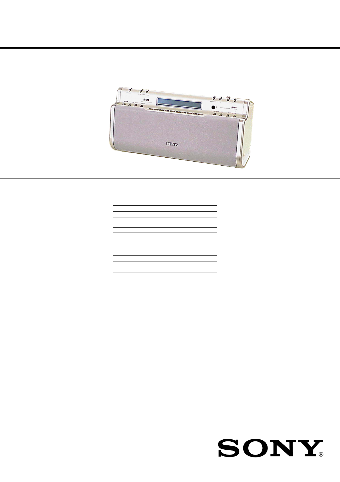
• LOCATION OF CONTROLS
SECTION 1
GENERAL
XDR-S1
This section is extracted
from instruction manual.
3
XDR-S1
)
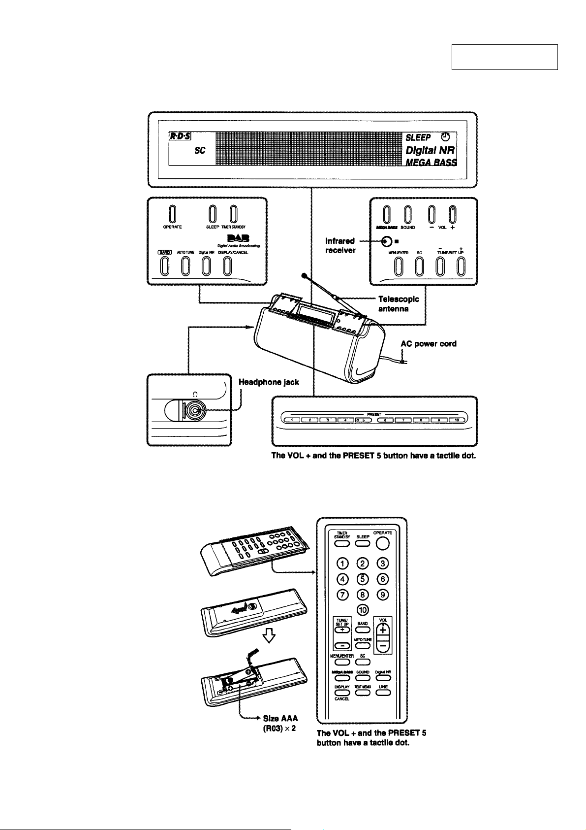
SECTION 2
DISASSEMBLY
• The equipment can be removed using the following procedure.
SET
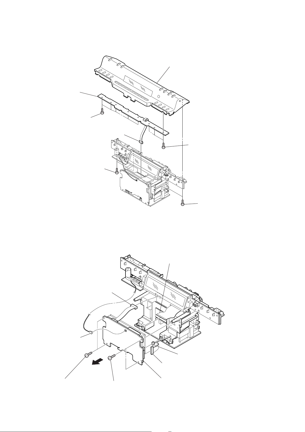
2-1. CABINET (REAR) ASSY
(Page 4)
2-2. WIRES
(Page 5)
2-3. CABINET UPPER ASSY
(Page 5)
2-4. KEY BOARD
(Page 6)
2-5. TUNER BOARD
(Page 6)
2-6. MICON BOARD
(Page 7)
2-7. POWER BOARD,
JACK BOARD
(Page 7)
Note : Follow the disassembly procedure in the numerical order given.
2-1. CABINET (REAR) ASSY
6
cabinet (rear) assy
four claws
2
four
screws
BV tapping (B3)
(+
)
5
two
screws
BV tapping (B3)
(+
)
4
two
screws
BV tapping (B3)
(+
3
four
screws
1
net assy
BV tapping (B3)
(+
)
4
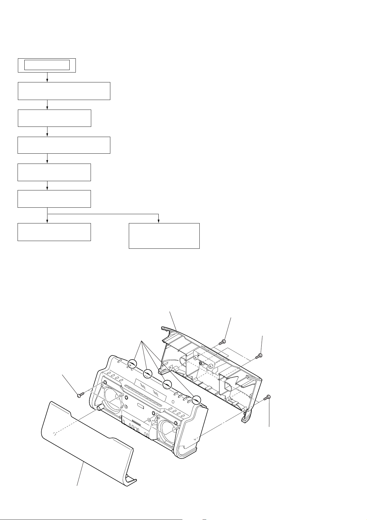
2-2. WIRES
a
Put flat cable and wires between the cabinets and push them in the
grooves located at A to D in the figure to prevent disconnection
before assembling the set.
XDR-S1
front side
2-3. CABINET UPPER ASSY
2
CN304 (9P)
1
CN302 (4P)
AB CD
8
cabinet upper assy
7
two
screws
(+
BV tapping (B3)
6
two
screws
(+
BV tapping (B3)
)
5
telescopic antenn
)
cabinet front assy
3
CN301 (6P)
4
screw
(M3x6 lock ace)
terminal (antenna)
5
XDR-S1
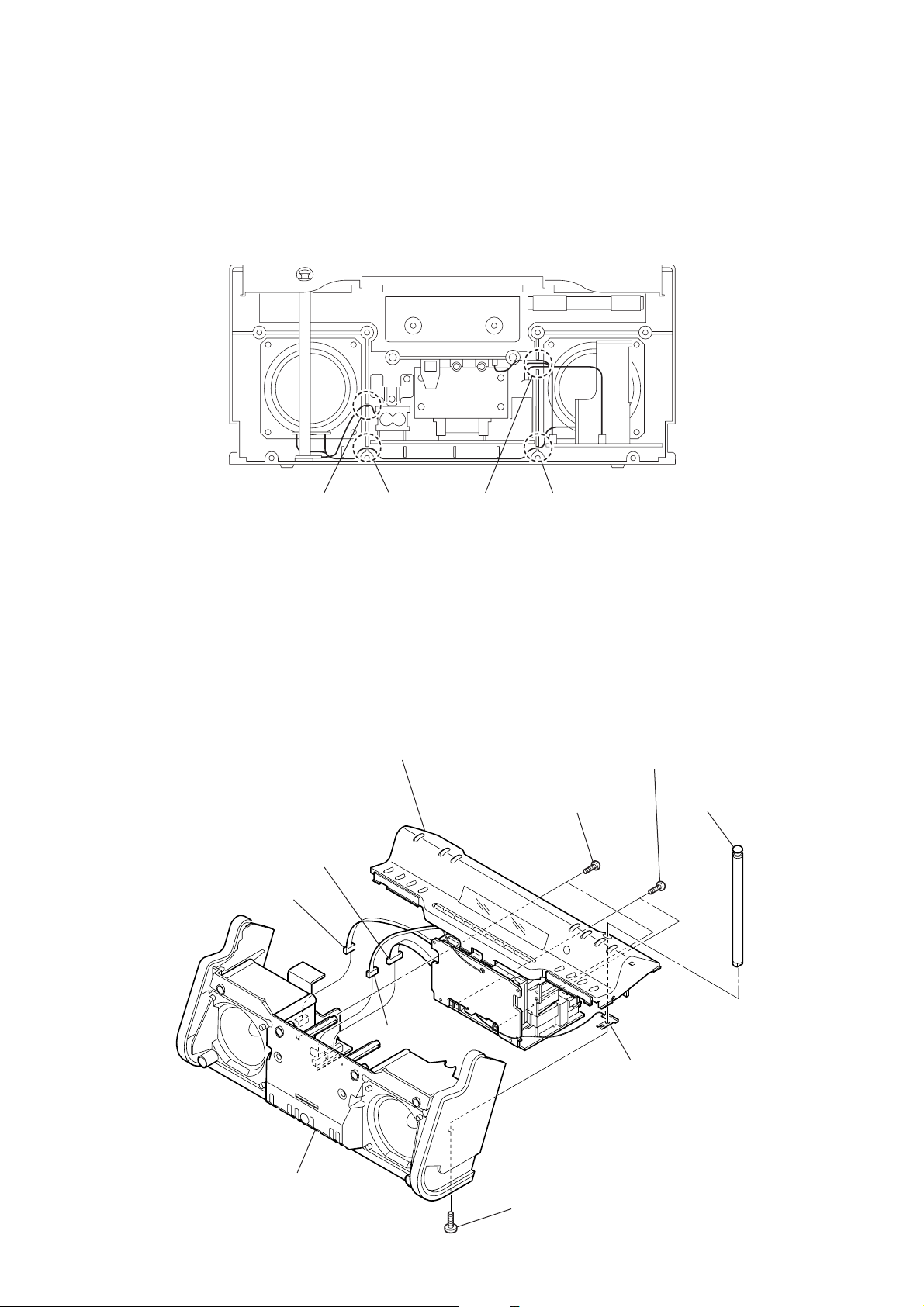
2-4. KEY BOARD
6
7
KEY board
five
screws
(+
P tapping (B2.6)
)
1
CN702 (4P)
4
cabinet upper assy (SVX)
5
three
screws
(+
P tapping (B2.6)
)
2-5. TUNER BOARD
3
two
screws
(+
P tapping (B2.6)
7
CN704 (6P)
)
2
two
screws
(+
8
CN502 (22P)
P tapping (B2.6)
)
1
CN501
2
CN504 (3P)
6
CN503 (9P)
9
TUNER board
3
two
screws
(+
P tapping (B2.6)
5
4
two
)
screws
P tapping (B2.6)
(+
)
6
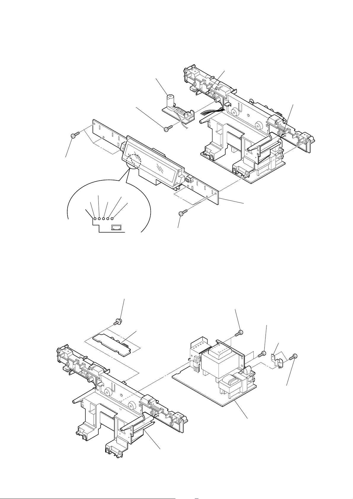
2-6. MICON BOARD
4
three
screws
(+
P tapping (B2.6)
1
screw
(+
P tapping (B2.6)
)
2
helical antenna
)
XDR-S1
claw
claw
green
red
3
Remove the five solderings.
black
yellow
natural
2-7. POWER BOARD, JACK BOARD
1
two
(+
PWH tapping (B2.6)
2
screws
JACK board
5
three
screws
(+
P tapping (B2.6)
)
6
MICON board
)
6
two
screws
(+
BV tapping (B3)
)
5
two
screws
(+
BV tapping (B3)
4
)
bracket (AC inlet)
chassis
7
POWER board
3
two
screws
(+
BV tapping (B3)
)
7
XDR-S1
SECTION 3
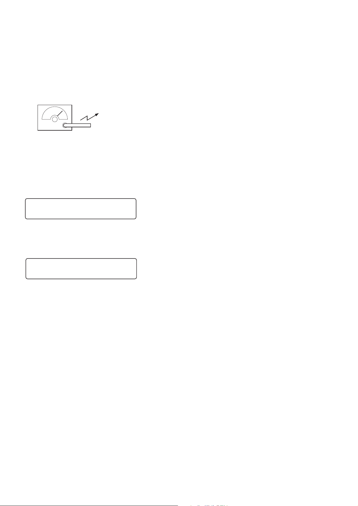
ELECTRICAL ADJUSTMENTS
TRACKING ADJUSTMENT
This set has the calibration function for tracking adjustment. It is
calibrated on each of LW and MW bands using frequencies at 7
points or 9 points.
Setting:
BAND: MW or LW
AM RF signal
generator
Put the lead-wire
antenna close to
the set.
30% amplitude
modulation by
400 Hz signal
• LW
1. With the power of f, press the 4 ke ys: [TIMER STANDBY], [SC],
0 and [DISPLAY] simultaneousl y for 3 seconds. The LCD
display shows “Calibration Mode” on the top and “LW MW
EXIT” on the bottom.
Calibration Mode
LW MW EXIT
2. Select “LW” using the TUNE/SET UP [+]/[--] key, and press
the [MENU/ENTER] key.
3. The LCD display shows “Calibration” on the top and the
frequency at 1st point “153 kHz” on the bottom.
• MW
1. Select “MW” using the TUNE/SET UP [+]/[--] key, and press
the [MENU/ENTER] key .
2. The LCD display shows “Calibration” on the top and the
frequency at 1st point “531 kHz” on the bottom.
3. Set the output frequency of the signal generator to 531 kHz.
4. When adjustment at 1st point is completed (it takes for about 3
seconds), press the [MENU/ENTER] key.
5. Repeat steps 2 to 4 until adjustment at 2nd point to 9th point is
completed.
Frequency at each point:
1st point: 531 kHz
2nd point: 603 kHz
3rd point: 702 kHz
4th point: 801 kHz
5th point: 900 kHz
6th point: 999 kHz
7th point: 1305 kHz
8th point: 1503 kHz
9th point: 1602 kHz
6. Once adjustment at all the points is completed, the LCD display
shows “Complete Cancel” on the top. Select either of the
following options using the TUNE/SET UP [+]/[--] key and press
the [MENU/ENTER] key .
Complete: Writes the data and returns to the menu.
Cancel: Aborts the data and returns to the menu.
• Termination of Adjustment
1. Select “EXIT” using the TUNE/SET UP [+]/[--] key, and press
the [MENU/ENTER] key .
2. The LCD display shows “Please Reset”. Press the [RESET] ke y
to terminate the Calibration Mode.
Calibration
153kHz
4. Set the output frequency of the signal generator to 153 kHz.
5. When adjustment at 1st point is completed (it takes for about 3
seconds), press the [MENU/ENTER] key.
6. Repeat steps 3 to 5 until adjustment at 2nd point to 7th point is
completed.
Frequency at each point:
1st point: 153 kHz
2nd point: 162 kHz
3rd point: 174 kHz
4th point: 186 kHz
5th point: 195 kHz
6th point: 243 kHz
7th point: 279 kHz
7. Once adjustment at all the points is completed, the LCD display
shows “Complete Cancel” on the top. Select either of the
following options using the TUNE/SET UP [+]/[--] key and press
the [MENU/ENTER] key.
Complete: Writes the data and returns to the menu.
Cancel: Aborts the data and returns to the menu.
8
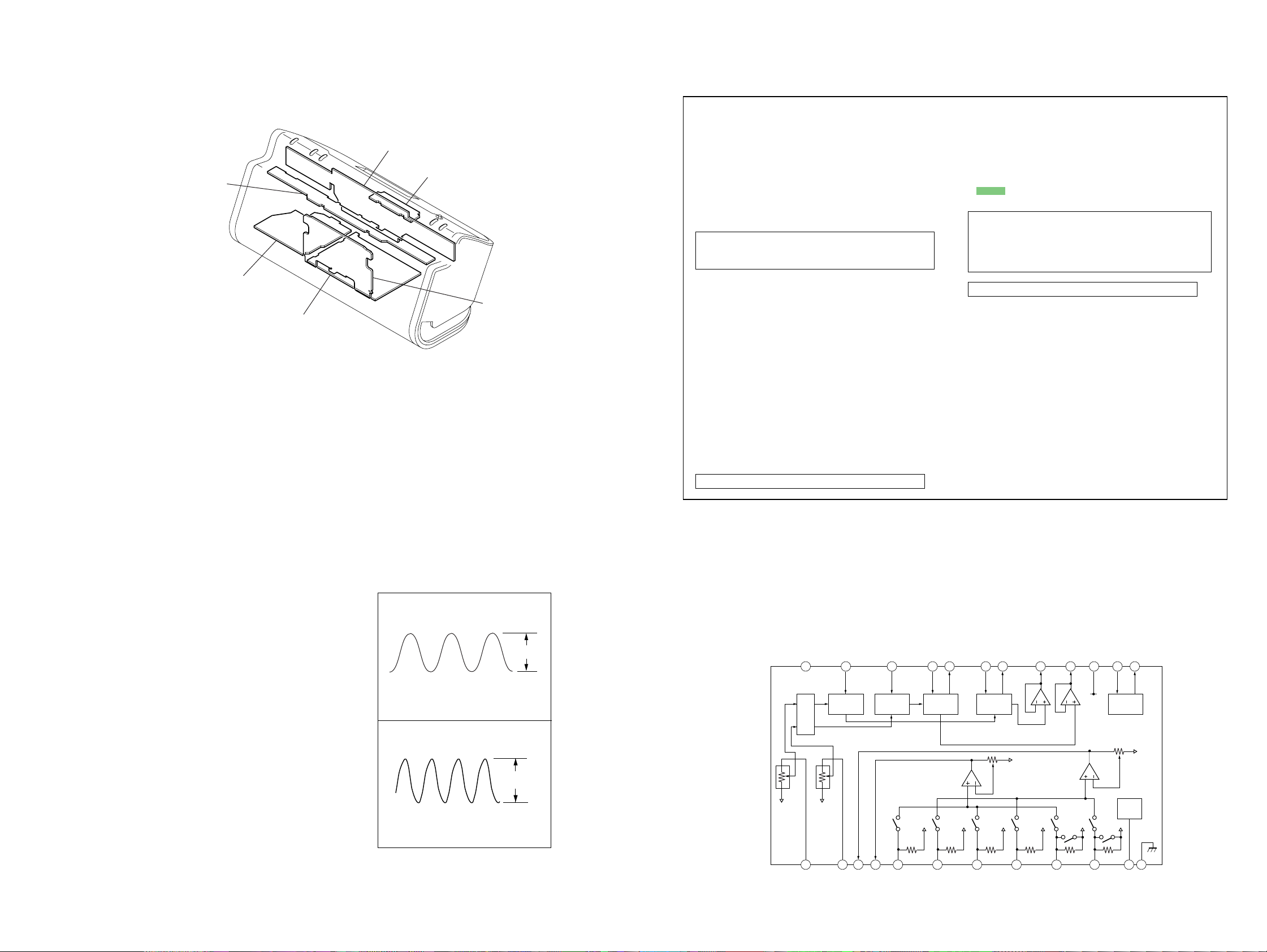
SECTION 4
d
VIN1
VIN2
SEL2
SEL1
A1
A2
B1
B2
C1
C2
FILTER
GND
CAP
TNF1
TNF2
BNF2
BOUT2
BNF1
BOUT1
OUT1
OUT2
SI
SC
VCC
BASS1
f
0
=80Hz
BASS2
f0=80Hz
21 20 19 18 17 16 15 14 13
TREBLE2
f
0
=8kHz
22
TREBLE1
f
0
=8kHz
23
SURROUND
24
1 2 3 4
LOGIC
VCC/2
VCC/2
VCC/2 VCC/2
VCC/2
5 6 7 8 9 10 11 12
DIAGRAMS
• CIRCUIT BOARDS LOCATION • NOTE FOR PRINTED WIRING BOARDS AND SCHEMATIC DIAGRAMS
THIS NOTE IS COMMON FOR PRINTED WIRING
BOARDS AND SCHEMATIC DIAGRAMS.
(In addition to this, the necessary note is
MICON board
JACK board
KEY board
AUDIO board
TUNER boar
POWER board
printed in each block.)
for schematic diagram:
• All capacitors are in µF unless otherwise noted. (p: pF)
50 WV or less are not indicated except for electrolytics
and tantalums.
• All resistors are in Ω and 1/
specified.
4
W or less unless otherwise
• C : panel designation.
Note: The components identified by mark 0 or dotted line
with mark 0 are critical for safety.
Replace only with part number specified.
• A : B+ Line.
•Voltage and waveforms are dc with respect to ground
under no-signal conditions.
no mark : FM
(): MW
<>: LW
•Voltages are taken with a VOM (Input impedance 10 MΩ).
Voltage variations may be noted due to normal production tolerances.
•Waveforms are taken with a oscilloscope.
Voltage variations may be noted due to normal production tolerances.
• Circled numbers refer to waveforms.
• Signal path.
F : FM
f : MW
E : DAB
j : LW
for printed wiring boards:
• X : parts extracted from the component side.
• Y : parts extracted from the conductor side.
• : Pattern from the side which enables seeing.
(The other layer’s patterns are not indicated.)
Caution:
Pattern face side: Parts on the pattern face side seen from
(Side B) the pattern face are indicated.
Parts face side: Parts on the parts face side seen from
(Side A) the parts face are indicated.
✩ When IC701 is damaged, replace the MICON board.
XDR-S1
• WAVEFORMS — MICON BOARD —
IC701 uk (XOA)
1
1.8Vp-p
32.768kHz
500 mV/DIV 0.1 msec/DIV
i;
IC701
2
(XO)
1.3Vp-p
✩ When IC701 is damaged, replace the MICON board.
• IC BLOCK DIAGRAM
IC303 BD3870FS-E2 (AUDIO Board)
XDR-S1
4.19MHz
500 m V/DIV 0.5
µ
sec/DIV
99
 Loading...