

Page 1
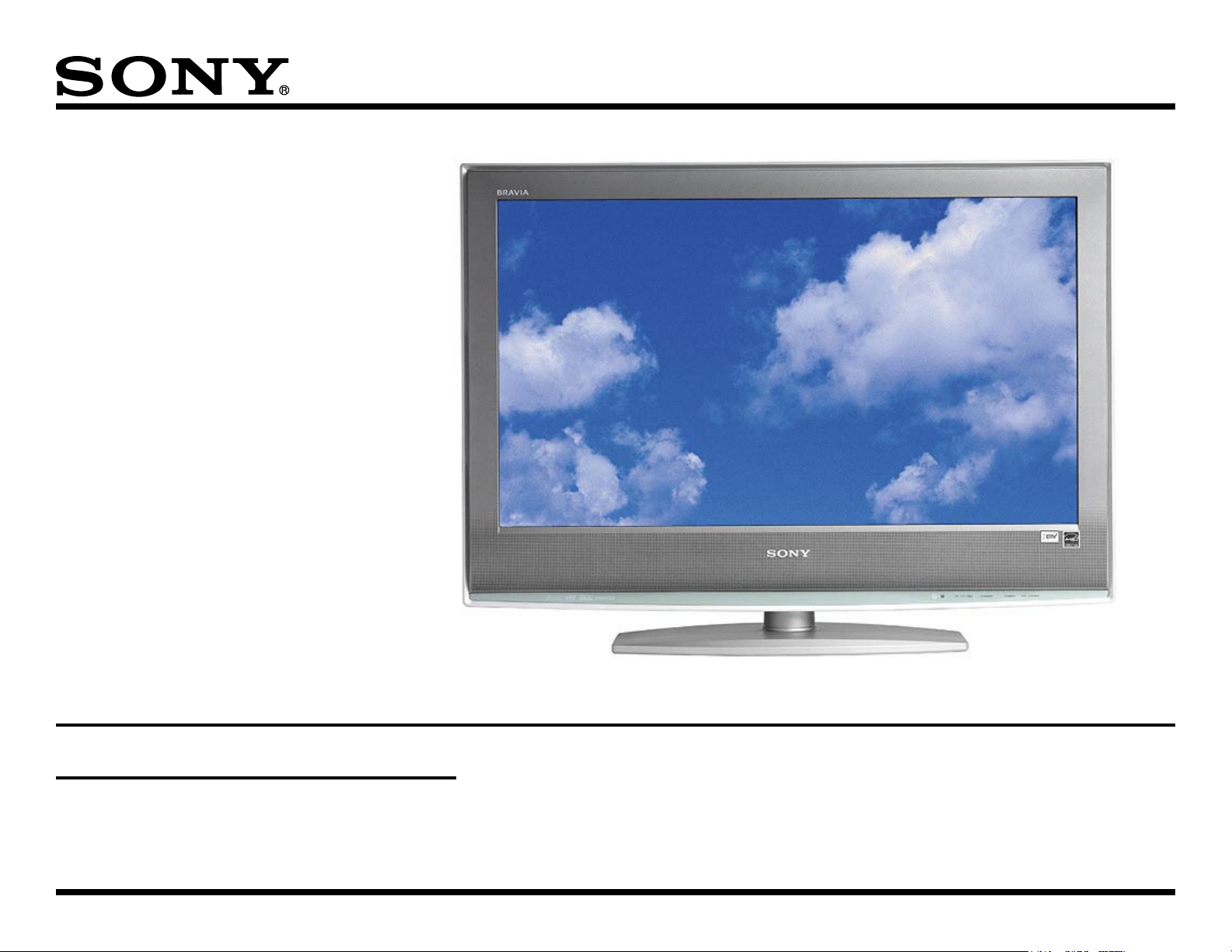
WAX2 Chassis Direct-View LCD
Models:
Training Manual
KDL-26S2000
KDL-32S2000
KDL-40S2000
KDL-46S2000
Diagnostics and Troubleshooting
Course: CTV-38R3
Page 2
Table of Contents
Introduction .......................................................................... 1
Overview .......................................................................... 1
Models Covered ................................................................... 1
TV Specifications ................................................................. 1
Features ............................................................................... 2
About This Manual ........................................................... 2
Chapter 1 - Overall System Block & Board Descriptions 3
Overall TV System Block Diagram .................................. 3
Board Location Diagram .................................................. 4
PCB and Module Descriptions ......................................... 5
LCD Panel Assembly LCD Panel Assembly ........................ 5
Backlight Inverter Board (Lamp Power Supply) ................... 5
G1-Board (26” & 32”) & G2-Board (40” & 46”) Power Supply) ...........
5
AU-Board (Audio/Video Switching, System Control, & Audio
Processing) .................................................................... 5
BU-Board (Video Processing) .............................................. 6
Overall System Description ........................................... 12
DC Power Supply System ................................................. 12
Backlight Inverter Board (Lamps Power Supply) ............... 13
Power-ON Sequence ..................................................... 14
Troubleshooting Tips ..................................................... 15
Main & Standby Power Supply .......................................... 15
Backlight Inverter Board (Lamps Power Supply) ............... 16
Chapter 3 - Protection System ......................................... 17
Protection System Block Diagram 1 .............................. 17
Protection System Block Diagram 2 .............................. 18
Overall System Description ........................................... 20
Protection Circuits Functional Description ........................ 20
10.5V Over-Voltage & Panel 5V Low-Voltage Protection
(1X Flash Pattern) .................................................. 20
D5V Low-Voltage Protection (2X Flash Pattern) .......... 20
3.3V, 2.4V, & 1.8V LVP-Voltage Protection (3X Flash Pat-
tern) ........................................................................ 21
QS-Board ............................................................................. 6
QT-Board ............................................................................. 6
H1-Board ............................................................................. 6
H2-Board ............................................................................. 6
H3-Board ............................................................................. 6
Chapter 2 - Power Supply System ..................................... 7
Troubleshooting Tips ..................................................... 25
Backlight Protection (4X Flash Pattern) ....................... 21
Overall Power Supply Protection (5X Flash Pattern) ... 22
Audio Output Protection (6X Flash Pattern) ................ 23
Internal Temperature Protection (7X Flash Pattern) .... 23
TRIDENT Protection (8X Flash Pattern) ...................... 24
10.5V & Panel 5V Low-Voltage Protection (1X) ........... 25
Power Supply Block Diagram .......................................... 7
Component Location Diagram ......................................... 8
D5V Under-Voltage Protection (2X) ............................. 25
3.3V & 1.8V Low-Voltage Protection (3X) .................... 25
CTV-38 i
Page 3

Table of Contents
Backlight Protection (4X) ............................................. 25
Overall Power Supply Protection (5X) ......................... 26
Audio Output Error (6X) ............................................... 27
Internal Temperature Protection (7X) ........................... 27
TRIDENT (Scan Converter) Protection (8X) ................ 27
Chapter 4 - Video Processing System ............................. 28
Video System Block Diagram ........................................ 28
Component Location Diagram ...................................... 29
BU-Board Connectors & IC Locations .......................... 30
On-Screen-Displays (OSD) Diagram ............................ 31
Overall System Description ........................................... 33
Video Circuits Functional Description ................................ 34
Troubleshooting Tips ..................................................... 35
No Video or Distorted Video Troubleshooting .............. 35
Video Input Troubleshooting ........................................ 35
Chapter 5 - Audio Processing System ............................. 37
Factory Reset ...................................................................... 3
White Balance Adjustment ................................................... 4
Digital Channel Information & Status ............................... 5
System Status ...................................................................... 5
Front End Status .................................................................. 6
Internal Pattern Generators ............................................. 7
PATN ................................................................................... 7
GPTN ................................................................................... 8
Audio System Block Diagram ........................................ 37
Component Location Diagram ....................................... 38
Overall System Description ........................................... 40
Troubleshooting Tips ..................................................... 41
Appendix ............................................................................... 1
Service Mode Options ..................................................... 1
Acessing Service Adjustments ............................................. 1
Acessing Digital & Analog Service Options ......................... 2
CTV-38 ii
Page 4
Introduction
Overview
Models Covered
KDL-26S2000 KDL-40S2000
KDL-32S2000 KDL-46S2000
TV Specifications
Display Resolution: 1,366 (dots) x 768 (lines)
HDMI Input: Video - 480i, 480p, 720p, and 1080i
Audio - 2 channel Linear PCM
PC Input:
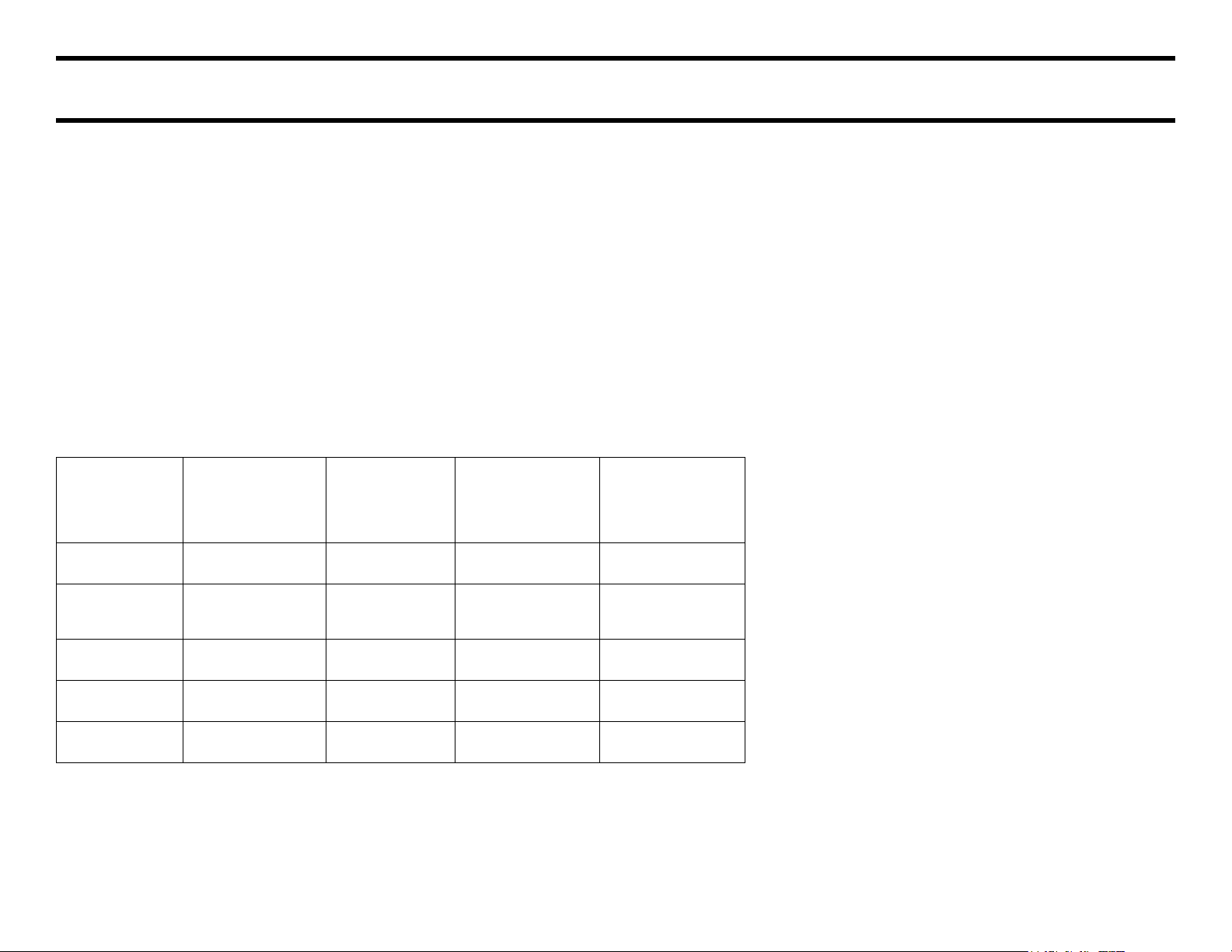
Table A – PC Input Signal Compatibility Chart (Best Results)
Signal
Format
VGA 640 480 31.5 60
Horizontal
(Pixel)
Vertical (line)
Horizontal
Frequency
(kHZ)
Headphone Output Impedance: 16 ohms
Power Consumption:
In Use
KDL-26S2000 - 120W
KDL-32S2000 - 150W
KDL-40S2000 - 200W
KDL-46S2000 - 240W
In Standby
All Models - Less Than 0.1W
Vertical
Frequency (Hz)
SVGA 800 600 37.9 60
XGA 1024 768 48.4 60
WXGA 1280 768 47.8 60
SXGA 1280 1024 64 60
Speaker Impedance: 8 ohms
Speaker Output: 10W x 10W
CTV-38 1
Page 5

Technologies & Features
Features
Digital/Analog Channels Selection
This feature places the TV in either an all analog channels or all digital
channels list. In previous models analog and digital channels where all
included in a single channel list. When one of the modes is selected the
other is not available. For example, if the Digital Mode is selected, only the
available digital channels wil be displayed and no analog are available.
To view the analog channels place the TV in the analog mode.
About This Manual
This manual is designed to help you understand the function, operation,
and diagnostic procedures of the major components (or boards) in the
WAX2 chassis TV models. The level of knowledge gained will enable you
to effectively troubleshoot and repair all the models containing the WAX2
chassis.
Reference the CTV-38 TTS (Triage & Troubleshooting) Guide for the
Triage Summary Sheet and Troubleshooting Flowcharts for the models
civered in this manual.
The diagrams, descriptions, and procedures in this manual are based
on the KDL-26/32/40/46S2000 models. However, the information given
can be easily adapted to troubleshoot other WAX2 and WAX2F chassis
models in the following list. The only differences are in the component
reference number and possible the part number. Therefore, confirm all
reference and part numbers for are models other then the S2000 series.
KDL-26S2010 KDL-40S20L1
KDL-32S2010 KDL-40V2500
KDL-32S2400 KDL-46S2010
KDL-32S20L1 KDL-46V2500
KDL-40S2010 KDL-46V25L1
KDL-40S2400
Each chapter contains a simplified block diagram of the particular system
(Power Supply, Protection, Video, and Audio) and connector/testpoint
photographs or diagrams. The diagrams only contain the connectors that
are easily accessible for probing when troubleshooting.
Each chapter also includes brief circuit theory of operation and circuit
(component) troubleshooting sections.
The appendix includes service mode displays and adjustments relevant
to field diagnostics and repair.
CTV-38 2
Page 6
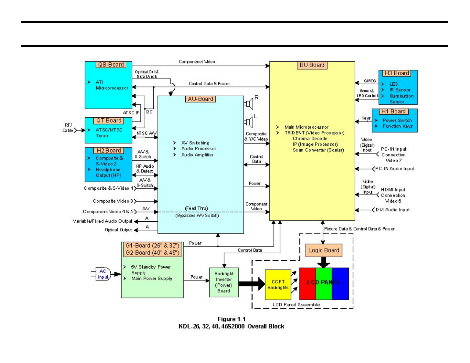
Chapter 1 - Overall System Block & Board Descriptions
Overall TV System Block Diagram
CTV-38 3
Page 7
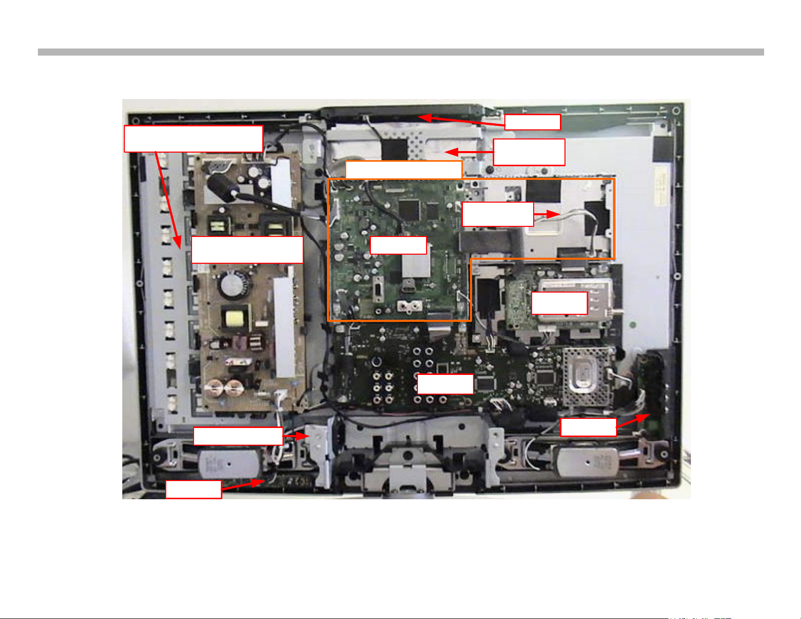
Board Location Diagram
G1-Board (26" & 32")
G2-Board (40" & 46")
BU-Board
AU-Board
QT-Board
H2-Board
H1-Board
H3-Board
Logic Board
Under Shield
Backlight Inverter Board
Under G-Board and Shield
QS-Board
Under Shield
Top Shield Removed
Figure 1-2
KDL-26, 32, 40, 46S2000 Board Location
AC Inlet Module
1. Overall System Block
CTV-38 4
Page 8

1. Overall System Block
PCB and Module Descriptions
Reference Figures 1-1 & 1-2
LCD Panel Assembly LCD Panel Assembly
Included as part of the LCD Panel Assembly is the Logic Board, Backlight
Lamps, and the LCD Panel.
The Logic Board performs pixel addressing, charging, and discharging
functions.
Backlight Inverter Board (Lamp Power Supply)
CCFT’s require a high voltage to start the current flowing from cathode to
anode. Typically 1000+ VAC This voltage causes the mercury to ionize,
releasing electrons from the molecules. Once ionized, the voltage drops
to a nominal level, approximately 400-450 VAC. The Backlight Inverter
board takes the DC 17V from the Main Power Supply and converts (or
inverts) the DC voltage into and AC voltage. The initial AC voltage output
is ~ 1000V lamp ignition voltage and then the output is regulated down to
~ 400VAC for normal lamp operation.
G1-Board (26” & 32”) & G2-Board (40” & 46”) Power Supply)
Except some regulator circuits on the BU-Board, the G1-Board or G2Board is the power supply system board, which includes the following
components and circuits.
• AC Inlet Module
• Main Fuse (F6101)
• Standby 3.3V Power Supply
o 3.3V
• Main Power Supply
o 18.5V
o 10.5V
o 15V
• Power Factor Circuit (PFC)
• Inrush Current Relay
AU-Board (Audio/Video Switching, System Control, & Audio Processing)
The A3U-Board performs all the analog video and audio switching functions.
The following video and audio inputs are switched on this board.
Video Input Switching:
• Video Inputs 1, 2, 3 (Composite & S-Video)
• Video Input 4, 5 (Component) Note: The component is not
switched, but does pass through the AU-Board to the BU-Board)
• NTSC Analog Video Signal
Audio Input Switching:
All audio inputs are switched on the AU-Board.
• Audio Inputs 1, 2, 3 (Composite)
• Audio Inputs 4, 5 (Component)
• NTSC Analog Audio Signal
Audio Input Direct to DSP:
• Audio Input 6 (HDMI/DVI)
• Audio Input 7 (PC-IN)
Audio Outputs:
• Optical Digital Audio Output
• Variable/Fixed Audio Output
Audio Processing:
The following circuits are also located on the AU-Board.
• Audio DSP
• Digital Audio Amplifier
CTV-38 5
Page 9

1. Overall System Block
• Headphone Audio Amplifier
• Variable/Fixed Audio Amplifier
BU-Board (Video Processing)
The circuits located on the BU-Board perform all video processing
functions (It is the WEGA engine). The following inputs and circuits are
included on the BU-Board.
Video Inputs Directly to TRIDENT:
• Video Input 6 (HDMI/DVI)
• Video Input 7 (PC-IN)
• Video Input 4, 5 (Component)
• ATSC Digital Video Signal
TRIDENT Video Processor IC
The following circuits are included in the TRIDENT IC
• Composite/Component Processor (CCP)
• Digital Reality Creator (DRC)
• Scan Converter
Microprocessor:
Board. The IF-signal is further demodulated and decoded to produce the
digital component output from the QS-Board.
QT-Board
The QT-Board contains the RF Tuner and NTSC signal processing circuits.
The QT-Board demodulates the terrestrial RF signal, and supplies an IFSignal to the QS-Board (ATSC) and a Composite video signal (NTSC) to
the AU-Board video switching circuits.
H1-Board
• Power Button
• Channel Up/Down Button
• Volume Up/Down Button
• TV/Video Button
• Menu Button
H2-Board
• Front Video 2 Input (S-Video, Composite, Audio LR)
• Headphone Jack
• Main Microprocessor
Voltage Regulators
• A9V Regulator
• 1.8V Regulator
• 3.3V Regulator
• 10.5V & Panel 5V Switching Regulator
• 5V Regulator
H3-Board
• Front Panel LED’s (Power, Standby, and Picture OFF/Timer)
• IR Sensor
• Illumination Sensor
QS-Board
The QS-Board contains all the ATSC signal decoding and processing
circuits. The RF Tuner on the QT-Board supplies the IF-Signal to the QS-
CTV-38 6
Page 10
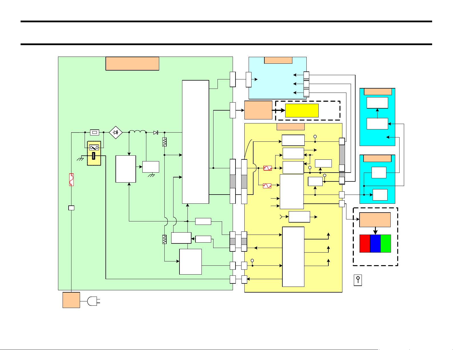
Power Supply Block Diagram
BU-Board
10.5V
15V
18.5V
IC7000
Switching
Regulator
IC1006
1.8V Reg
3.3V
F7000
PS7000
F6101
AC Input
D6101
RY6101
R6102
CN6202
CN6200
IC7002
1.8V Reg
CN7008
STBY 3.3V
Q6102
IC6301
PFC
L6103
19V
D6114
18.5V
IC7001
3.3V Reg
IC1010
A9V Reg
Power ON
(Power 1)
Panel 5V
D5V
A9V
IC6104
Standby
3.3V
Power
Supply
Power 2
Power 4
Power 3
AC
Inlet
Module
CN6102
Switch
Circuit
Figure 2-1
KDL-26, 32, 40, 46S2000 Power Supply Overall Block
Relay ON
4
G1-Board (26" & 32")
G2-Board (40" & 46")
AU-Board
IC6501
Main
Power
Supply
9
\
12
Backlight
Inverter
Board
19V
LCD
PANEL
IC1001
Main
Micro
5
4
STBY 3.3V
STBY
3.3V
7
\
8
13
\
14
IC7005
5V Reg
1
\
2
10.5V
3
4
1
QT-Board
QS-Board
33V Reg
Tuner
1.8V
1.8V
3
4
1
REG
REG
D5V
3
10.5V
A9V
D5V
D3.3V
D3.3V
Power 3
Power 4
Power 2
CCFL
Backlights
Logic
Board
LCD
Panel
Assb
LCD Panel
Assembly
3
VCC
VCC
A15V
R6505
R6169
CN6203
CN6202
10
1
\
2
CN7503
CN9502
CN6202
CN6200
CN6202
CN6200
CN6203
CN6202
CN6203
CN6202
CN5000
CN4701
CN6202 (G1)
CN6200 (G2)
CN6203 (G1)
CN6202 (G2)
NOTE:
VSense
PH6103
CN7009
CN1002
CN7009
7
\
8
13
\
14
CN1002
3.3V
(Power 5)
PH6101
3
2
AC-OFF DET
5
6
Voltage used for
On-Board Circuits
IC7004
2.4V Reg
Chapter 2 - Power Supply System
CTV-38 7
Page 11
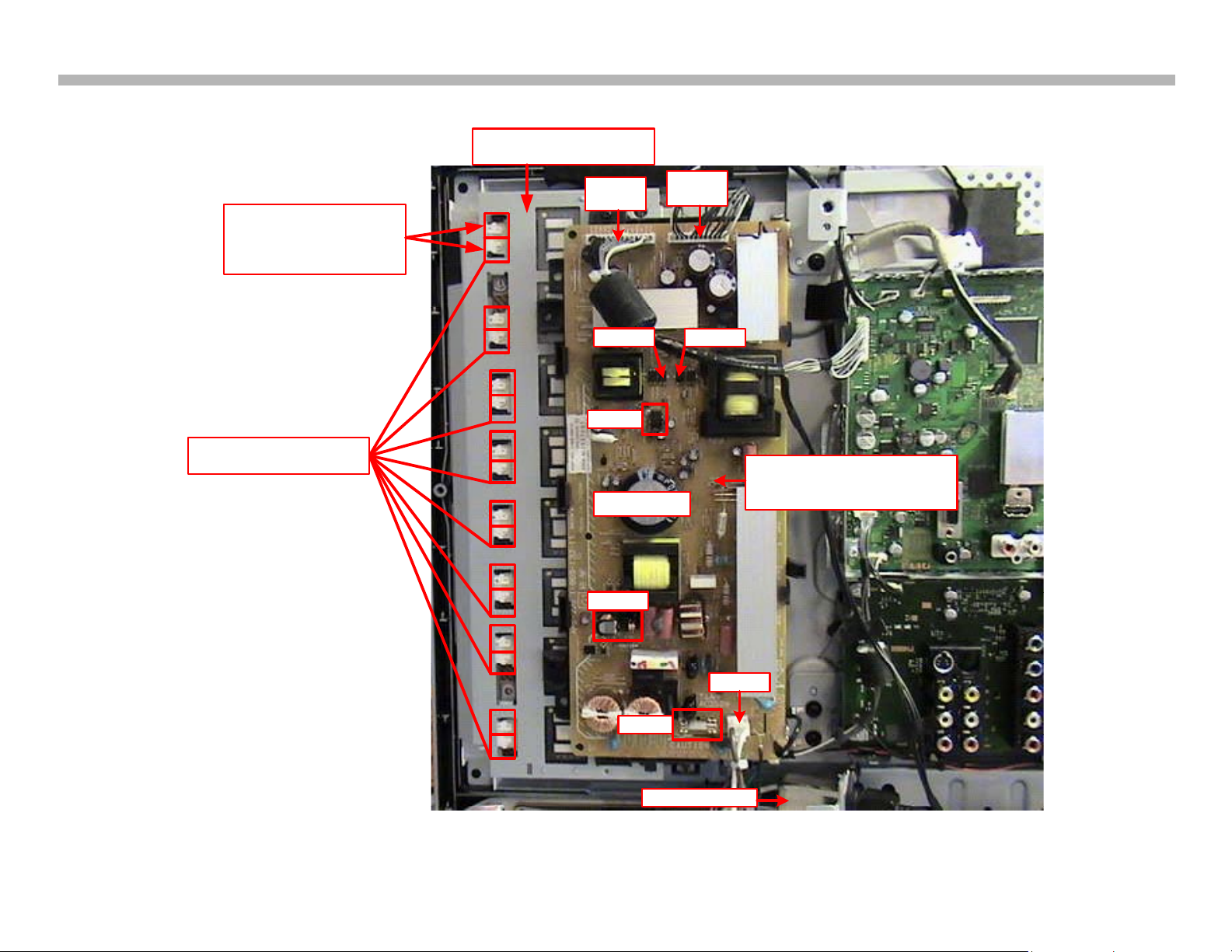
Component Location Diagram
CN6202
CN6200
CN6102
F6101
Figure 2-2
KDL
-26, 32, 40, 46S2000 G2/G2-Board Connector & Component Locations
CN6200
CN6203
IC6104
PH6103
PH6101
AC Inlet Module
IC6501
Main Power Supply
(Non-Conponent Side of Board )
RY6101
G1-Board
Backlight Inverter Board
(Under Shield)
CCFL connectors
(2 Lamps per connector )
Place VOM (set to AC volts)
probe on both top sides of
connectors
(~ 3VAC)
indicates good output
2 Power Supply System
CTV-38 8
Page 12
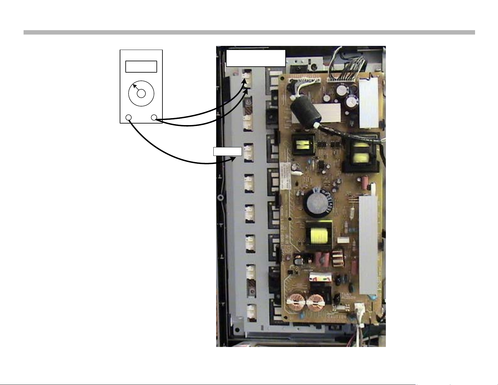
2 Power Supply System
3.00ACV
ACV
+-
VOM
Ground
Place probe on top
of plastic connector
Figure 2-3
Backlight Inverter Board Test
CTV-38 9
Page 13
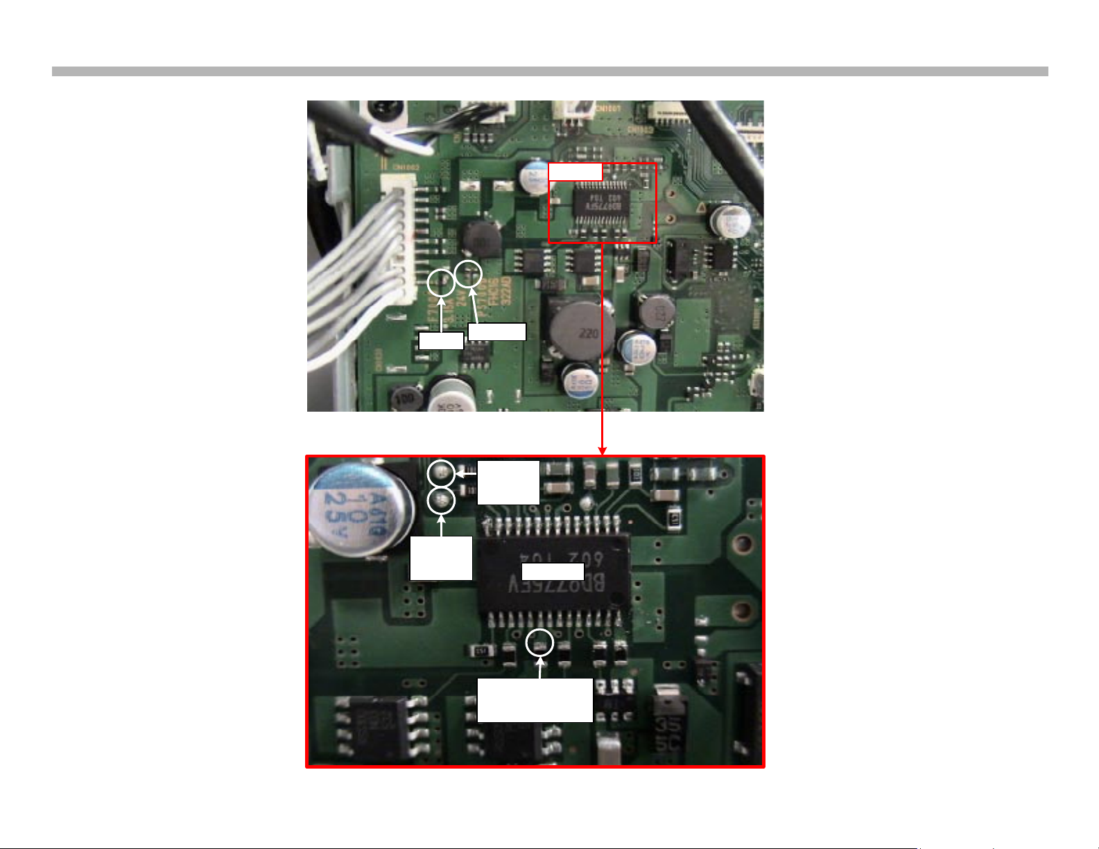
Panel 5V
TP
1
(topside of resistor )
Power 3
(3.3V)
TP5
F7000
PS7000
IC7000
IC7000
TP - Test Point
Power 4
(3.3V)
TP6
2 Power Supply System
Figure 2-4
KDL-26, 32, 40, 46S2000
BU-Board Regulator, Test
Points, and Fuses
CTV-38 10
Page 14
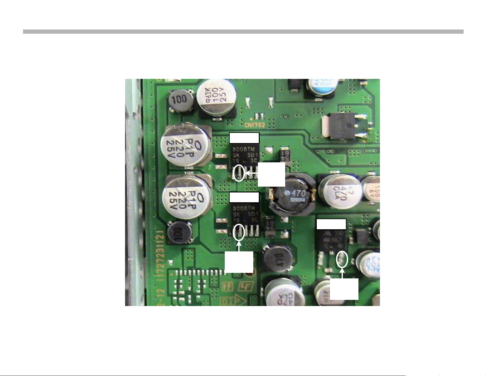
2 Power Supply System
TP2
(1.8V)
TP3
(3.3V)
IC7001
IC7002
TP4
(2.4V)
IC7004
Figure 2-5
KDL-26, 32, 40, 46S2000 BU-Board Regulators and Test Points
CTV-38 11
Page 15

2 Power Supply System
Overall System Description
DC Power Supply System
Reference Figures 2-1
The power supply system for the WAX2 chassis televisions consists of
the Standby (STBY) 3.3V Power Supply, Main Power Supply, and the
Power Factor Control (PFC) circuit. Aside from various regulator circuits,
all power supply circuits are contained on the G1/G2-Board. The G1Board is used in the 26”, 32”, and 40” models, while the G2-Board is used
in the 46” model. The only differences between the two power supply
boards are an extra connector, which supplies extra 18V lines to the Panel
Assembly, and different component and connector reference numbers.
The basic operational functions and troubleshooting procedures discuss
in this section can be applied to both the G1-Board and G2-Board.
Both the Standby 3.3V and Main Power Supplies are switch-mode power
supplies. The configuration and operation is similar to previous models.
This section will discuss effective and efficient methods to troubleshoot
these circuits.
The AC (110V) is supplied through the AC Inlet Module, which contains
the AC line filter. The AC voltage passes through the main fuse F6101
and is applied directly to the Main Power Supply and Standby 3.3V Supply
through the InRush Relay & Resistor (R6102) and relay (RY6004) and
the Standby 3.3V converter (IC6300). The AC power initially passes
through R6102 to limit the initial current surge, which occurs when the TV
is first turned on. The AC power is also applied directly to the Standby
3.3V Power Supply. Consequently, as long as the TV is plugged into the
AC outlet the Standby 3.3V circuit is activated and supplying STBY 3.3V
to Main Microprocessor (BU-Board), IR Sensor (H3-Board) as shown
in Figure 3-1. The Standby 3.3V places the TV Microprocessor and IR
Sensor in standby mode waiting for an ON command from the remote
control or the ON/OFF main unit button on top of the TV.
upon power ON. The PFC circuit’s purpose is to make the power supply
circuits look like a purely resistive load to the external AC power network
(current and voltage are in-phase). In reality the internal switch-mode
power supply circuit is a highly inductive load (current and voltage are
90 degrees out-of-phase, which causes distortions and inefficiencies in
the AC power network when connected directly (no PFC circuit in place).
Therefore, the PFC circuit enables the TV to use the AC power more
effectively and efficiently.
The Main Power Supply circuit IC6501 develops and supplies all other
operating voltages (18.5V, 10.5V, 15V) throughout the television as shown
on Figure 3-1. The Main Power Supply activates once an “ON” command
is received and the Inrush Relay is activated. The microprocessor on the
BU-board supplies the “Relay-ON” and “Power-ON” signals (CN7009/pin
4 & 6) respectively. The InRush Relay coil is activated by the high “RelayON” signal, and the relay switch closes. The relay switch bypasses the
InRush Resistor R6102, the resistor is basically removed from the AC
input circuit. The AC power is then applied directly to the Main Power
Supply.
To complete the Main Power Supply turn-on sequence the “Power-ON”
signal goes high to activate the switch circuit through PH6103, which will
then apply 19V from the Standby 3.3V Power Supply IC6104 to the Main
Power Supply IC6501 VCC. The 19V is also used to power up the PFC
circuit.
Once the Main Power supply is up and running all the secondary voltages
(18.5V, 10.5V, 15V) are developed.
There are seven regulators on the BU-Board:
• IC1010 9V Regulator
• IC7002 1.8V Regulator
• IC7001 3.3V Regulator
• IC7000 10.5V Regulator
The Standby Power Supply also applies a rectified and filtered 19V through
the switch circuit to the PFC circuit when the TV is powered on. The 19V
supply ensures that the PFC circuit will condition the AC input immediately
• IC7000 Panel 5V Regulator
• IC7005 5V Regulator
• IC1006 1.8V Regulator
CTV-38 12
Page 16

IC7000 develops the Panel 5V, which is supplied to the Logic Board (part
of the LCD Panel Assembly).
IC7000 is dual package switching regulator, which also develops the 10.5V
used to develop the D5V (IC7005) and to power the QS-Board, which in
turn develops voltages to power the QT-Board. The D5V remains on
the BU-Board, and is also sent to the AU-Board to power various digital
circuit.
IC1010 develops the A9V. The A9V powers the A/V Switcher IC2001,
Audio DSP IC7001, Digital Amplifier, and several of audio amplifiers on
the AU-board.
IC7002 and IC1006 both develop the 1.8V, which powers various circuits
on the BU-board.
IC7001 develops the 3.3V, which powers the Optical Audio Output LED
on J9003.
Notice that IC7002, IC7001, and IC7000 all have “Power” control signals
(Power 2, Power 3, and Power 4) supplied from the Main Microprocessor
on the BU-Board. In most cases if one of these signals is missing a
protection mode activates, and the TV shuts down. Therefore, these signals
will be used as test points in particular Protection Mode troubleshooting
procedures in Chapter 4.
2 Power Supply System
Backlight Inverter Board (Lamps Power Supply)
CCFT’s require a high voltage to start the current flowing from cathode to
anode. Typically 1000+ VAC This voltage causes the mercury to ionize,
releasing electrons from the molecules. Once ionized, the voltage drops
to a nominal level, approximately 400-450 VAC. The Backlight Inverter
board takes the DC 17V from the Main Power Supply and converts (or
inverts) the DC voltage into and AC voltage. The initial AC voltage output
is ~ 1000V lamp ignition voltage and then the output is regulated down to
~ 400VAC for normal lamp operation.
CTV-38 13
Page 17
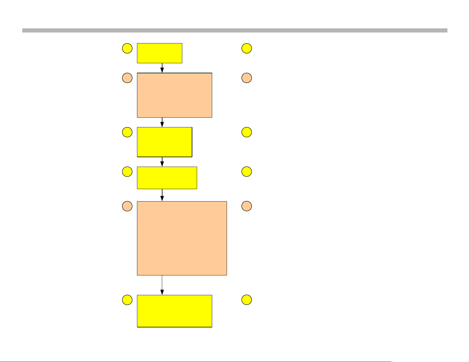
Power-ON Sequence
AC Power
Applied
Standby 3.3V - ON
InRush Relay - OFF
Main Micro - Standby
IR Sensor – ON
PFC Circuit - OFF
“ON” Command
Received
(Main Micro)
“Power-ON” - HIGH
“RELAY-ON” - HIGH
InRush Relay – ON
Main Power Supply – ON
All Regulators – ON
I2C Microprocessor
communications – Active
PFC Circuit - ON
Green Power-LED
Illuminates
Green Power-LED
Glows Steady
(Unit ON)
1
2
3
4
5
6
1
2
3
4
5
6
The AC power cord is plugged into the AC outlet and is
applied to the G
1/G2-Board.
The AC voltage supplied to the G
1/G2-Board is applied
directly to the InRush -Relay and the Standby 3.3V power
supply circuit. The Standby
3.3V is applied to the Main
Micro and places it into standby mode. It also turns ON
the IR sensor.
The Main
-Microprocessor located on the BU -Board
receives a ON command when either the ON
/OFF button
is pressed on the remote or the TV top panel
.
The Green Power
-LED on the TV front panel illuminates
immediately after an ON command is received and
processed.
The Green Power
-LED remains illuminated.
The Main Microprocessor sends the following signals
Power
-1: Main Power Supply IC6501 (Power-ON)
Power
-2: IC7001 (3.3V Reg) & IC7002 (1.8V Reg) ON
Power
-3: IC7000 (10.5V Output) ON
Power
-4: IC7000 (Panel 5V Output) ON
The Main Power Supply IC6501 turns ON and all the
television operating voltages are developed.
The “Relay
-ON signal turns ON the InRush Relay, which
bypasses the InRush resistor .
All microprocessor I2C communications commence.
After all the power supply voltages and microprocessor
communications have been successfully develop the
Green Power LED will glow steady
.
The Power-ON sequence is completed.
2 Power Supply System
KDL-26,32, 40, 46S2000
Power-ON Sequence Diagram
Figure 2-6
CTV-38 14
Page 18

2 Power Supply System
Troubleshooting Tips
Main & Standby Power Supply
Reference Figures 2-1 & 2-6
When troubleshooting a “Unit will not turn ON” problem in previous
models the Red Standby LED was very helpful. It indicated that at least
the Standby Power Supply was functioning when lit. Unfortunately, there is
no Red Standby LED on any of the WAX2 chassis models. Consequently,
the only visual check to determine if the Standby 3.3V Power Supply is
functioning is to press the ON/OFF Power button and watch for the Power
LED on the front panel to illuminate Green.
If the Power LED illuminates Green when the Standby 3.3V power
supply and the Main Microprocessor (this processor controls the
LEDs) are functioning. A steady glowing Green Power LED indicates
successful Power-ON sequence (ref. Figure 2-6) and Microprocessor
communications.
If the Power LED glows steady with no video or audio present check
the 10.5V at CN6202 or CN6200/pin 7 on the G1/G2-Board and D5V
at CN7008/pin 3 on the BU-Board. A loss of either of these voltages will
cause this condition. Furthermore, checking these voltages will determine
if the failure exists on the G1/G2-Board or BU-Board.
The 10.5V is produced by the Main Power Supply IC6501 on the G1/G2Board and the D5V is produced by the 5V regulator on the BU-Board.
Therefore, if the 10.5V is missing a CN6202 or CN6200 then the failure
exists on the G1/G2-Board — replace the G1/G2-Board.
However, if the D5V is missing at CN7008 then the failure exists on the
BU-Boad — replace BU-Board.
NOTE: A loss of D5V due to a power supply failure will trigger the protection
mode circuits. Therefore, you only need to confirm proper connection of
the D5V wiring harness (or damaged wiring).
If the voltages & connections are OK and the Power LED is steady Green
but there is still no video and audio, you should redirect your troubleshooting
efforts to the video and/or audio sections.
If the Power LED begins flashing Red then the Main Microprocessor has
detected a system failure and has placed the TV in a particular Protection
Mode. The Red LED flash pattern (number of flashes – LED ON, should
between LED pauses – LED OFF) should be noted. The pattern indicates
the particular failure that has occurred. For example, a Red LED flashing
5 times between pauses (5X) indicates a general power supply failure.
Let us go back and analysis the situation where the Power LED does not
light Green after the TV receives an “ON” command.
The first step in troubleshooting a “No Green Power LED” condition is
to confirm that the TV is securely plugged into an active AC (110VAC)
outlet.
NOTE: Plug a typical house lamp into suspect AC outlet to confirm an
active 110VAC output. Furthermore, note lamp brightness to determine
and active but low AC voltage output.
If the AC outlet checks OK, then the next step is to confirm that the AC
voltage is applied to the G1/G2-Board. Check for 110VAC at CN6102 on
the G1/G2-Board. If 110VAC is not present, check for a damage AC cord
or plug. If all connections are OK replace the AC Input Module.
If 110VAC is present at CN6102 perform the following checks.
1) Check the Main Fuse (F6101) on the G1/G2-Board
2) Check for Standby 3.3V
You can use an Ohmmeter or AC Voltmeter to check for a defective Main
Fuse. The fuse should read 0 ohms or have 110VAC on both side with
reference to Hot Ground (white wire on CN6102). Replace fuse if open. If
the new fuse opens again replace the G1/G2-Board.
If the Main Fuse checks OK, then AC voltage will be applied directly to the
Standby Power Supply and 3.3V is developed at the supply output. Check
for 3.3V at CN6202 or CN6200/pin 5 on the G1/G2-Board.
Missing 3.3V indicates a defective Standby Power Supply – replaced the
G1/G2-Board.
The presence of 3.3V indicates the Standby Power Supply is functioning.
The next step is to confirm the 3.3V is making it to the BU-Board and the
Main Microprocessor. Check for the 3.3V at CN1002/pin 10 on the BU-
CTV-38 15
Page 19

Board.
Missing 3.3V indicates a loose or damaged connection between the G1/
G2-board and the BU-Board. Secure or repair connections.
The presence of 3.3V indicates a defect on the BU-Board or a defective
Main Microprocessor – replace the BU-Board.
Backlight Inverter Board (Lamps Power Supply)
Reference Figures 2-1, 2-2, & 2-3
Caution: Do not attempt to directly measure the Backlight Inverter Board
output directly. 1000V or greater is present at the outout on initail power
ON.
The best way to check the Inverter Board output is to place your VOM
probe on top of the individual plastic lamp connectors (reference Figure 22 & 2-3). Set the VOM to AC volts, place the probe on top of the connector
directly above one of the two wires (each connector feeds two lamps).
Place the VOM probe over each wire for proper measurements.
A good output will measure approximately 3VAC.
2 Power Supply System
A bad output will measure aproxiamatey 1VAC or less.
If any single output is bad replace the Backlight Inverter Board.
If all Inverter Board outputs are bad, check the 18V supply voltage from
the Main Power supply before replacing the Backlight Inverter Board.
If the 18V is missing check for loose or damaged connections between
the G1/G2-Board and the Backlight Inverter Board.
If the 18V is present at the Inverter Board, however, all output are bad
then replace the Backlight Inverter Board.
CTV-38 16
Page 20
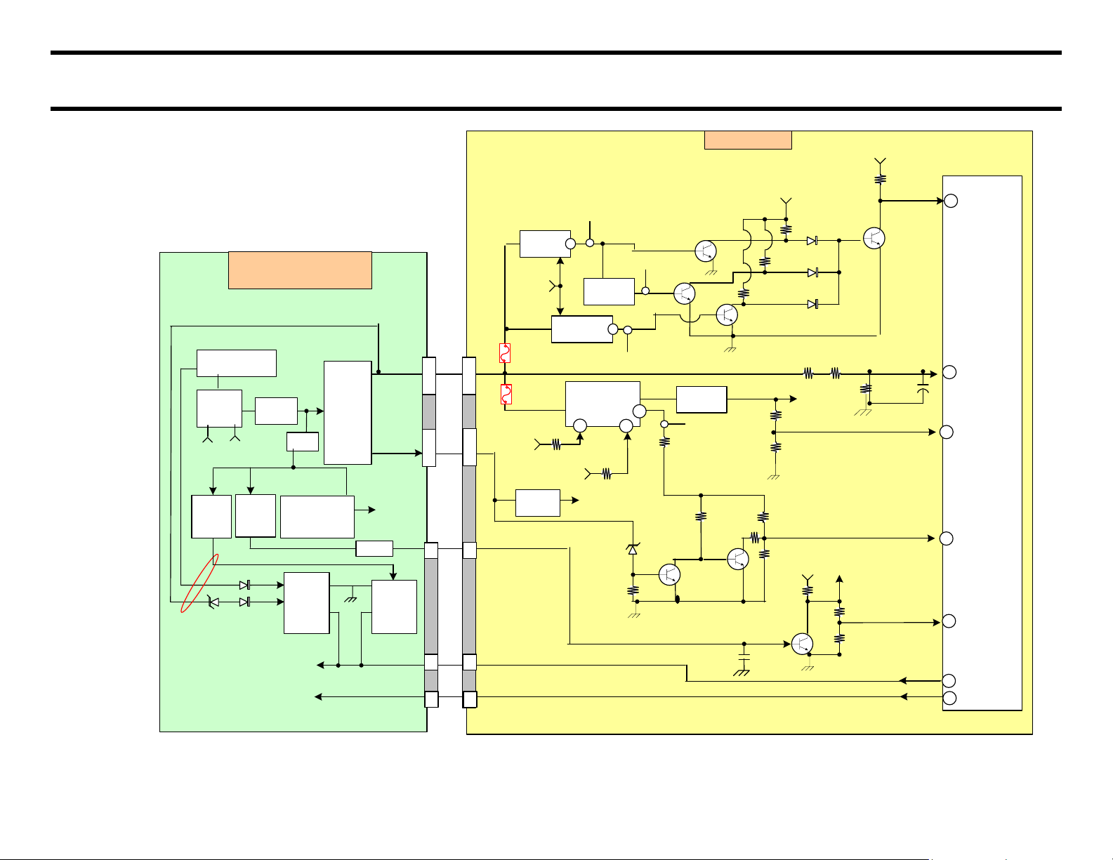
Chapter 3 - Protection System
BU-Board
DC Alert 3
D7500
4.7V
CN6200
CN6202
IC6100
Main
Power
Supply
PFC
DC Alert 1
DC Alert 2
PS7000
A9V
Power-ON
3.1V
3.1V
3.1V
3.3V
18.5V
10.5V
3X
2X
IC1001
TV
Micro
1X
0V
5.8V
IC6300
Standby 3.3V
Power Supply
RY6101
InRush
Relay
D6000
OVP &
InRush
Latch
Q6202
Q6204
Inrush Relay
Monitor Circuit
To IC6100 Thru
Switching Circuit
5X
0V
0V
AC
Input
STBY
3.3V
CN6202
CN6203
F7000
D6407
22V
D7508
R7517
Q7500
Q7502
Figure 3-1
KDL-26,32, 40, 46S2000 Failure Protection System Overall Block
PH6101
G1-Board (26" & 32")
G2-Board (40" & 46")
OVP
Latch
Q6105
Q6107
19V
OVP
Circuit
AC-OFF DETECT
0.1V
Panel 5V
IC7000
10.5V &
Panel 5V
Reg
R7507
R7506
R7518
7
\
8
13
\
14
1
\
2
5X
STBY 3.3V
Q7503
Q7506
Q7505
Q7504
R7542
R7543
R7544
R7516
R7515
D7509
D7510
R1037
R1034R1031
3.1V
S1-OFF
AC-OFF DETECT-AU
(Audio Mute)
A9V
3.1V
R1046
R1047
R1048
(Main Power Lose)
DC Det
Power 1
Q1002
3.3V
1.8V
IC7005
D5V Reg
10.5V
D5V
R7510
C1100
R7025
R7015
Power 3
(Panel 5V)
13
20
TP1
IC1010
9V Reg
R7014
Power 4
(10.5V)
7
\
8
12
2
3
5
6
CN7009
32
83
154
153
82
4
4
To RY6101
Inrush Relay
Relay-
ON
20
3.3V Relay-ON
Power 5
19V
19V
LVP
Circuit
IC7002
1.8V Reg
TP2
2
IC7004
2.4V Reg
IC7001
3.3V Reg
2
TP3
2.4V
D5V
R7545
163
C1007
TP4
Power 2
Protection System Block Diagram 1
CTV-38 17
Page 21
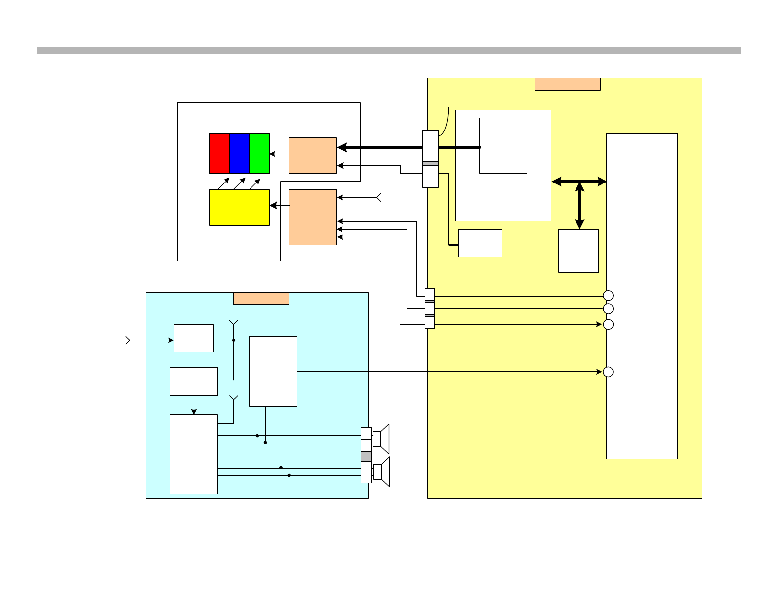
Protection System Block Diagram 2
BU-Board
IC1007
Temp
7X
I2C
Bus
IC1001
TV
Micro
Figure 3-2
KDL
-26, 32, 40, 46S2000 Video, Temperature, Audio Protection Circuits
Backlight
Inverter
Board
LCD Panel Assemble
AU-Board
Scan
Converter
Internal
Failure
8X
IC5000
Trident
(Video Processor)
Logic
Board
6X
4X
Audio Protect
Panel Detect
IC7007
Digital
Audio
Amplifier
DC Detect
Q7014
Q7015
Q7016
Q7017
Q7018
Q7021
R
L
Backlight (ON)
CN1001
Digital Video
LCD
Panel
Backlights
2.8V
3.1V
3.2V
7X & 8X
1,3
5,7
9,11
17
,19
16,18
26
,28
29
CN5000
Panel 5V
IC2001
Audio
Switcher
IC7001
Audio DSP
A9V
Audio
Inputs
18.5V
G1-Board
CN6203
IC7000
Switching
Regulator
2
3
CN7009
1
Dimmer
3
4
2
1
CN7000
Audio Protect
A15V
Min 0.7V
Max
2.4V
26
149
112
81
3. Protection Circuits
CTV-38 18
Page 22
X1001
16
.5MHz
132
88
44
1
176
STBY 3.3V
1.8V
Power 5 (Relay-ON)
Pin# 20
Power 1 (Power-ON)
Pin# 32
Audio-Protect
(6X)
Pin# 26
S1-OFF
Pin# 83
DC-Detect
(5X)
Pin# 82
Panel Detect
(4X)
Pin# 81
DC Alert 2
(2X)
Pin# 153
Dimmer
Pin# 149
DC Alert 3
(1X)
Pin# 154
DC Alert 1
(3X)
Pin# 163
Main Microprocessor
IC1001
3. Protection Circuits
Figure 3-3
KDL-26, 32, 40, 46S2000
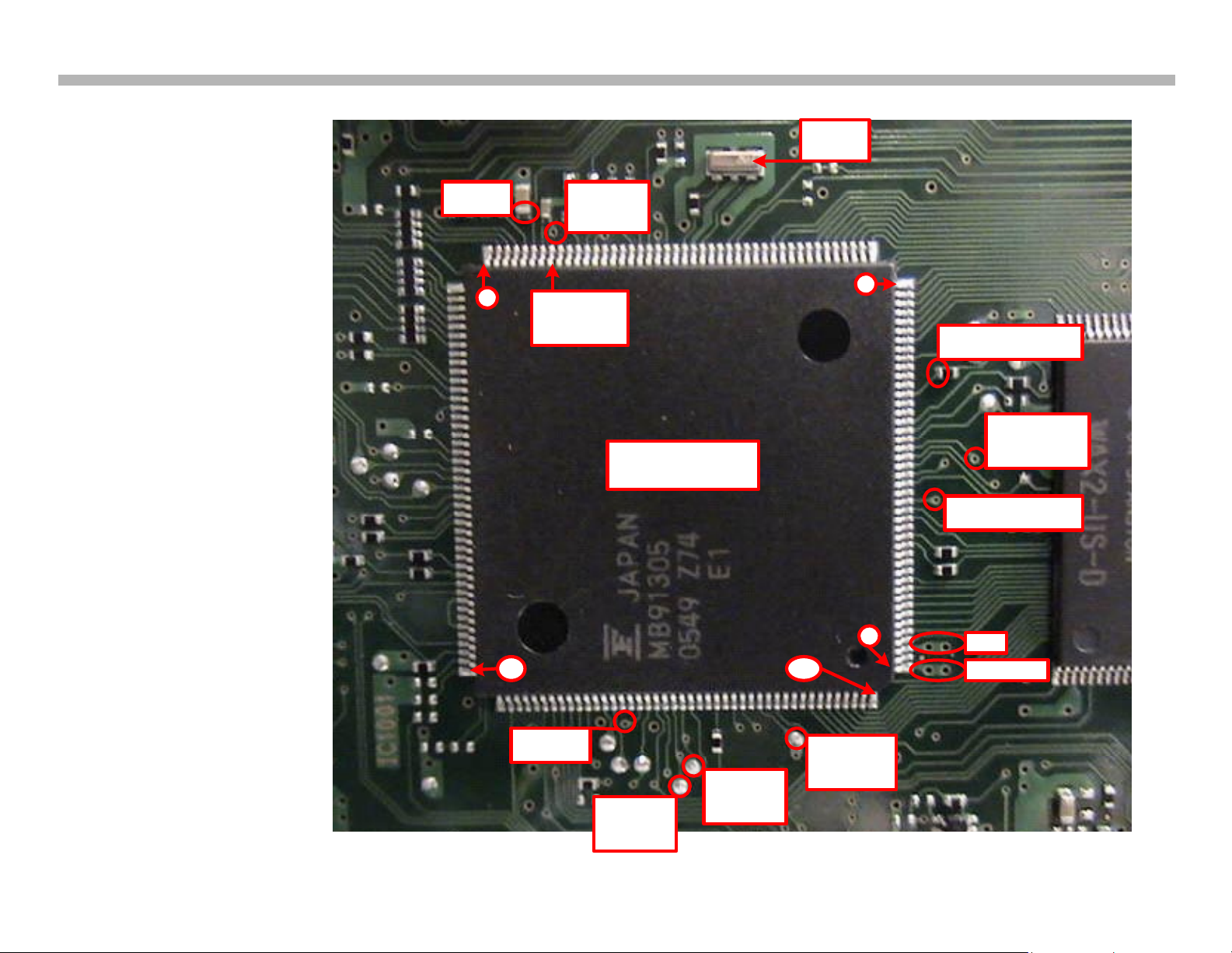
Main Microprocessor Key Pin
Locations on BU-Board
CTV-38 19
Page 23

3. Protection Circuits
Overall System Description
Reference Figure 3-1 & 3-2
The failure protection system (aka. self-diagnostics routines) for the WAX2
chassis monitors the following circuits for abnormal conditions. If the TV
microprocessor detects a failure it will activate the front panel Standby-
LED, which will flash a unique RED pattern depending on the failure that
occurred. The bullet list below lists all the monitored circuits and their
unique flash pattern.
• 10.5V & Panel 5V Low-Voltage Protection (DCALERT3)
1X Red Power-LED Flash Pattern
• D5V Low-Voltage Protection (DC ALERT 2)
2X Red Power-LED Flash Pattern
• 3.3V & 1.8V Low-Voltage Protection (DC ALERT 1)
3X Red Power-LED Flash Pattern
• Backlight Protection
4X Red Power-LED Flash Pattern
• Overall Power Supply Protection
5X Red Power-LED Flash Pattern
• Audio Output Protection
6X Red Power-LED Flash Pattern
• Internal Temperature Protection
7X Red Power-LED Flash Pattern
• TRIDENT (Scan Converter) Protection
8X Red Power-LED Flash Pattern
Protection Circuits Functional Description
NOTE: Make all voltage and signal measurements prior to the TV shuts
down, and goes into the Protection Mode. There is approximiately a
20-second window before shut down.
10.5V Low-Voltage & Panel 5V Low-Voltage Protection (1X
Flash Pattern)
Reference Figure 3-1
The service manual labels this protection mode as DC_ALERT 3. The
10.5V and Panel 5V supplies are monitored for a low-voltage condition.
The 10.5V is monitored by the 4.7V zener diode D7500 and transistors
Q7500 and Q7502 on the BU-Board. In normal operation D7500 is in the
breakdown mode (ON) as long as the 10.5V supply stays above 4.7V.
The zener has a voltage drop of 4.7V leaving 5.8V, which is applied to
the base of Q7500 turning Q7500 ON and Q7502 OFF. With Q7502 OFF
3.1V is developed at IC1001/pin 154 (Main Microprocessor) through the
voltage divider circuit of R7517 and R7518 using the Panel 5V supply
voltage from switching regulator IC7000.
If the 10.5V supply drops below 4.7V D7500 will turn OFF, Q7500 will turn
OFF and Q7502 will turn ON, and a ground is applied to IC1001/pin 154
pulling the pin low. Consequently, the Main Microprocessor detects a
10.5V failure and the Red Standby-LED flashes a 1X pattern and the TV
shuts down.
The Panel 5V is also monitor. The Panel 5V is the supply voltage to the
voltage divder R7517 & R7518. The voltage divder circuit at its mid-point
develops the 3.1V, which is applied to the Main Microprocessor. If the
Panel 5V is missing at the top of the diuvider circuit the 3.1V will go low
and the 1X protection mode is triggered.
D5V Low-Voltage Protection (2X Flash Pattern)
Reference Figure 3-1
The service manual labels this protection mode as DC_ALERT 2. The
D5V supply is monitored indirectly through the voltage divider consisting
of R7515 and R7516 on the BU-Board. IC7005 regulates the 10.5V (from
CTV-38 20
Page 24

3. Protection Circuits
the switching regulator IC7000) down to 5V. The 5V (or D5V) is then
applied to the Main Microprocessor IC1001/pin 153. If the D5V drops so
will the 3.1V at the mid-point of the voltage divider. Consequently, the
Main Microprocessor detects a D5V failure and the RED Standby-LED
flashes a 2X pattern and the TV shuts down.
3.3V, 2.4V, & 1.8V LVP-Voltage Protection (3X Flash Pattern)
Reference Figure 3-1
The service manual labels this protection mode as DC_ALERT 1.
This protection mode is activated if any one of the following regulators
failures.
• IC7001 3.3V Regulator
• IC7002 1.8V Regulator
• IC7004 2.4V Regulator
Each regulator output is monitored by a transistor and a diode. IC7001
is monitored by Q7504 and D7508; IC7002 is monitored by Q7506 and
D7510; IC7004 is monitored by Q7505 and D7509. The transistors are
ON in normal operation, turned ON by the voltage output of each regulator.
With the transistors ON a ground is applied to the anode of each diode,
therefore, each diode is OFF (or reverse biased). All three diode outputs
go to the base of a single transistor Q7503. The collector of Q7503 is
connected directly to the Main Microprocessor IC1010/pin 163.
In normal operation the voltage level at IC1001/pin 163 is 3.1V. If any of
the three regulators failure the corresponding transistor (Q7504, Q7505,
or Q7506) will turn OFF, and the ground is removed from the anode of the
corresponding diode (D7508, D7509, or D7510). With the ground removed
a high will be applied to the anode of the diode through the associated
pull-up resistor (R7542, R7543, R7544), and the diode will forward bias,
applying a high to the base of Q7503. The transistor turns ON applying
a ground to IC1001/pin 163 pulling the pin low. Consequently, the Main
Microprocessor detects a regulator failure and the RED Standby-LED
flashes a 3X pattern and the TV shuts down.
Backlight Protection (4X Flash Pattern)
Reference Figure 3-2
This protection mode monitors the operation of the Backlight Inverter
Board and the Lamps. The Inverter Board is the Lamp power supply,
which produces the high alternating voltage necessary to drive the ColdCathode Fluorescent Lamps (CCFL) used for the LCD panel backlighting.
There are three main causes for the activation of this protection mode.
• Loss of 18.5V supply to the Inverter Board (at CN6202 on the
G2-Board)
• Loss of 3.2V Backlight ON signal
• Defective Inverter Board Circuits
• Defective Lamp(s)
The following paragraphs are brief descriptions of each failure listed.
Loss of 18.5V supply to the Inverter Board (at CN6202 on the G2Board)
The 18.5V is the power supply for the Backlight Inverter board. However,
the 18.5V also drives two voltage regulators on the BU-Board (reference
Figure 3-1). Therefore, if the 18.5V is lost due to a Main Power Supply failure
a 5X flash pattern is generated. The Main Microprocessor generates a 4X
flash pattern only if there is a loss of 18.5V at CN6203. In other words,
the Main Power Supply is functioning OK (producing 18.5V), however,
the 18.5V is not making it to CN6203. There is a poor connection or
open circuit in the physical connection between the G1/G2-Board and
the Inverter Board. Consequently, the Backlight Inverter fails to start, the
Panel Detect line goes low (CN7009/pin 3), and the microprocessor
detects a failure.
Loss of 3.2V Backlight ON signal
Confirm 3.2V at CN7009/pin 1 on the BU-Board.
The Main Microprocessor on the BU-Board turns on the Backlight Inverter
using the 3.2V Backlight-ON signal. You can measure this voltage at
CN7009/pin 1 on the BU-Board. If the Main Microprocessor fails to send
this signal (rare occurrence) or if there is an open path (confirm secure &
undamaged connectors between the BU-Board and the Inverter Board)
CTV-38 21
Page 25

3. Protection Circuits
to the Backlight Inverter board then the Panel Detect line goes low
(CN8603/pin 4) and the microprocessor generates a 4X flash pattern.
Defective Inverter Board Circuits or Lamp Failure
Confirm 18.5V (Power Supply) and 3.2V (Backlight-ON).
In the case of an actual Backlight Inverter board circuit or Lamp failure, the
18.5V and the 3.2V voltages should be OK. Therefore, prior to shutdown
you can measure these voltages to confirm that power supply and control
signal are present. If these two voltages check OK, but the Backlight
does not light and the Panel Detect line goes low (CN8603/pin 4) then
the defect exists on the Backlight Inverter board or a Lamp(s) (Panel
Assembly) has failed. Use the following procedure to determine whether
the Backlight Inverter or the Panel Assembly is the defective component.
Caution: Do not attempt to directly measure the Backlight Inverter Board
output directly. 1000V or greater is present at the outout on initail power
ON.
The best way to check the Inverter Board output is to place your VOM
probe on top of the individual plastic lamp connectors (reference Figure 22 & 2-3). Set the VOM to AC volts, place the probe on top of the connector
directly above one of the two wires (each connector feeds two lamps).
Place the VOM probe over each wire for proper measurements.
A good output will measure approximately 3VAC.
A bad output will measure aproxiamatey 1VAC or less.
If any single output is bad replace the Backlight Inverter Board.
If all Inverter Board outputs are bad, check the 18V supply voltage from
the Main Power supply before replacing the Backlight Inverter Board.
If the 18V is missing check for loose or damaged connections between
the G1/G2-Board and the Backlight Inverter Board.
If the 18V is present at the Inverter Board, however, all output are bad
then replace the Backlight Inverter Board.
Overall Power Supply Protection (5X Flash Pattern)
Reference Figure 3-1
The purpose of this protection mode is to monitor and indicate a failure
of the Main Power Supply (IC6100) on the G1/G2-Board. The primary
voltage monitor is the 18V. If the Main Power Supply does start or remain
running the 18V will not be developed and the Main Microprocessor will
detect an overall power supply failure.
The 18V is applied to the voltage divider consisting of R1031, R1034,
and R1037. The voltage across R1037 (3.1V), which is stabilized and
delayed by C1007 is applied to the Main Microprocessor IC1001/pin82.
The presence of the 3.1V indicates a properly functioning Main Power
Supply. If the 18V is not developed for any reason, then the 3.1V is not
developed and the Main Microprocessor detects a power supply failure
(5X).
As illustrated on Figure 3-1 there is a multitude of failures that can cause
the Main Power Supply shutdown. The following list identifies the possible
failures.
• Failure of the Main Converter IC6100
• Loss of 3.3V Power-ON signal from Main Microprocessor
IC1001/pin 32
• Excessive 19V Supply to the PFC Circuit
• Failure of InRush Relay
• 18.5V Over-Voltage Condition
Main Power Supply Converter IC6100
Confirm that both the 3.3V Power-ON signal and the 18.5V increase, and
stabilize to their respective levels before protection-mode shutdown.
The presence of the 3.3V indicates that the converter IC6100 is most likely
getting the necessary VCC input, and the presence of the 18.5V indicates
that the converter IC6100 is starting and developing the secondary
voltages, therefore, some other fault is shutting the TV down.
It is rare that IC6100 will fail. This IC (MCZ3000D) integrated circuit has
been very reliable in many previous chassis’s.
CTV-38 22
Page 26

3. Protection Circuits
Loss of 3.3V Power-ON signal from Main Microprocessor
The Power-ON (or Power 1) signal is generate by the Main Microprocessor
IC1001/pin32 on the BU-Board. The tricky part about troubleshooting this
failure is determining if the Main Microprocessor is failing to generate the
Power-On signal or if one of the two latch circuits (Q6202/Q6204 & Q6105/
Q6107) on the G1/G2-Board is pulling the Power-ON signal low. Notice
that there are two latch circuits located on the G1/G2-Board. These latch
circuits connect directly to the Power-ON signal line.
If the Power-ON signal shows no signs of increasing towards 3.3V then the
most likely failure is the Main Microprocessor IC1001. Before replacing
the BU-Board check all connections between the BU-Board and G1/G2Board.
If the Power-ON signal increases to 3.3V and then goes to 0V, then one
of the latch circuits are being activated.
NOTE: The Power-ON signal can also be check unloaded. Disconnect
CN6202/CN6203 from the G1/G2-Board and check if the 3.3V is present. If
the 3.3V is present, then this indicates that the Latch circuits are activating
due to a failure on the G1/G2-Board and pulling the Power-ON line low.
One or more of the following events can trigger the latch circuits (reference
Figure 3-1)..
• Excessive 19V Supply to the PFC Circuit
• Failure of InRush Relay
• 18.5V Over-Voltage Condition
Loss of 18.5V (at CN7009 to the BU-board)
Confirm connections between G1/G2-Board and the BU-Board for the
18.5V path (reference Figure 3-1).
Audio Output Protection (6X Flash Pattern)
Reference Figure 3-2
The protection circuit (Q7014, Q7015, Q7016, Q7017, Q7018, and Q7021)
mounted on the AU-Board monitors the audio amplifier outputs (speaker
lines) for a shorted condition or for the presence of any DC voltage
level (positive or negative). If either of these conditions is detected the
protection circuit alerts the Main Microprocessor of the failure and the
Standby-LED Flashes a 6X flash pattern.
Internal Temperature Protection (7X Flash Pattern)
Reference Figure 3-2
The temperature sensor (IC1007) is mounted on the component side of
the BU-Board next to CN1700. IC1007 monitors the internal temperature
of the TV set, and communicates any temperature abnormality to the Main
Microprocessor over the I2C bus.
The following parameters affect internal temperature.
• TV Ventilation,
• Local External Temperature (Room Temperature)
• Internal Component Operating Temperatures
In most cases, one of the following actions will solve a temperature
failure.
• Clear the TV areas of ventilation
• Relocate the TV set away from any area heating elements
• Provide adequate space between TV cabinet and walls (at
least 4”)
• Replace Temperature Sensor IC1007
If the TV set shuts down immediately after turn-on and the Red StandbyLED indicates a temperature problem (7X flash pattern), then the most
likely failure is the temperature sensor IC1007. The reason for this
deduction is that a actual excessive temperature situation will take time
to occur. The internal TV temperature must increase and IC1007 must
detect the excessive temperature, and then communicate this information
CTV-38 23
Page 27

to the main Microprocessor. This whole process takes time. However, if
the temperature sensor (IC1007) itself has failed, the Main Microprocessor
will not be able to communicate with IC1007 when the TV is first turned
ON and the TV will, in comparison, immediately shut OFF.
TRIDENT Protection (8X Flash Pattern)
Reference Figure 3-2
TRIDENT is the name for the integrated circuit (IC5000) that includes all
the video processing circuitry, including the Scan Converter circuit. This
protection mode monitors the operation of the internal Scan Converter. A
failure of the Scan Converter is communicated over the I2C bus between
the TRIDENT and Main Microprocessor, and a 8X flash pettern will
occur.
3. Protection Circuits
CTV-38 24
Page 28

3. Protection Circuits
Troubleshooting Tips
10.5V & Panel 5V Low-Voltage Protection (1X)
Reference Figures 3-1, 3-2, and 2-1
The first step is to check that the Main Power Supply is developing 10.5V
at CN6200/CN6202/pins 7 & 8. The voltage should increase to 10.5V and
stabilize. If 10.5V in not present then the Main Power is defective, in this
case, replace the G1/G2-Board.
If the 10.5V is present the next step is to determine if the Panel 5V is being
developed by the switching regulator (IC7000) on the BU-Board. Check
the voltage at TP1 (Panel 5V) on the BU-Board, this is the 5V output of
IC7000. If the Panels 15V does approach 15V before the TV shuts down,
then the regulator has failed. In this case, replace the BU-Board.
If both the 10.5V and Panel 5V are OK then the protection circuit (Q7500
& Q7502) itself may have failed. If 3.1V is present at CN1001/pin 154 then
the protection circuit is working properly and the Main Microprocessor is
not processing the signal correctly. If 0V is present at CN1001/pin 154,
then the protection circuit has failed. In either case, you would replace
the BU-Board.
D5V Under-Voltage Protection (2X)
Reference Figures 3-1, 3-2, and 2-1
There are only two failures that can cause a 2X protection mode, they are
as follows.
• Open PS7000
• Defective 5V (D5V) regulator IC7005
Both components are located on the BU-Board, and therefore would
warrant are BU-Board replacement. However, for a possible quick and
easy fix check for an open PS7000. Replace if open.
If PS7000 is OK, then the output of the 5V regulator IC7005 should be
check to confirm a BU-Board failure. If the 5V is missing, then replace
the BU-Board.
3.3V & 1.8V Low-Voltage Protection (3X)
Reference Figures 3-1, 3-2, and 2-1
There are four failures that will cause a 3X protection mode state (all
located on the BU-Board), and they are as follows.
• Open F7000
• Defective 3.3V Regulator IC7001 (TP3)
• Defective 1.8V Regulator IC7002 (TP2)
• Defective 2.4V Regulator IC7004 (TP4)
If 0V is present at any of the regulator output test points or if F7000 is
open, then replace the defective component or the BU-Board.
If F7000 and all voltages (3.3V, 2.4V, and 1.8V) at the test points check
OK and the TV still shuts down (3X), then a component in the protection
circuit (Q7504, Q7505, Q7506, Q7503, D7508, D7509, and D7510) itself
may have failed.
Check for the presence of 3.1V at IC1001/pin 163. If 3.1V is present at
CN1001/pin163, then the regulators and protection circuits are working
properly. The failure is most likely the Main Microprocessor; it is not
processing the DC ALERT 1 signal properly. Replace the BU-Board.
Backlight Protection (4X)
Reference Figures 3-1, 3-2, and 2-1
The 4X protection occurs due to a failure of the Backlight-Inverter board
(failure to drive the Cold Cathode Fluorescent Lamps), or a defective Lamp.
Therefore, you will first check the 18.5V power supply for the BacklightInverter board at CN6203/CN6202/pins 9-12 on the G1/G2-Board.
The 18.5V comes directly from the G1/G2-Board to the Backlight-Inverter
board. Therefore, if the 18.5V is not present at CN6202/CN6203 then the
Main Power Supply has failed. Replace the G1/G2-Board.
If the 18.5V is present at CN6202/CN6203, then the next step is to
confirm that the Main Microprocessor is sending the “Backlight-ON” to
the Backlight-Inverter board.
The voltage at CN7009/pin 2 on the BU-Board should measure 3.2V in
CTV-38 25
Page 29

3. Protection Circuits
normal operation. If the 3.2V is not present then the Main Microprocessor
has failed. Replace the BU-Board.
If the 3.2V is present at CN7009, then the next step is to check the 3.1V
“Panel Detect” coming from the Backlight-Inverter board to the Main
Microprocessor. The Backlight-Inverter pulls the “Panel Detect” signal
to 0V when a failure occurs on the Inverter Board or if a Lamp fails. The
“Panel Detect” signal is measured at CN7009/pin 3.
If the voltage is 3.1V, then the Backlight-Inverter is working properly, and
attempting to communicate with the Main Microprocessor. However, the
Main Microprocessor is not processing the signal. In this case, replace
the BU-Board.
The presence of 0V at CN7009/pin 3 indicates a Backlight-Inverter failure.
Use the following procedure to determine whether the Backlight Inverter
or the Panel Assembly is the defective component.
Caution: Do not attempt to directly measure the Backlight Inverter Board
output directly. 1000V or greater is present at the outout on initail power
ON.
The best way to check the Inverter Board output is to place your VOM
probe on top of the individual plastic lamp connectors (reference Figure 22 & 2-3). Set the VOM to AC volts, place the probe on top of the connector
directly above one of the two wires (each connector feeds two lamps).
Place the VOM probe over each wire for proper measurements.
A good output will measure approximately 3VAC.
A bad output will measure aproxiamatey 1VAC or less.
If any single output is bad replace the Backlight Inverter Board.
If all Inverter Board outputs are bad, check the 18V supply voltage from
the Main Power supply before replacing the Backlight Inverter Board.
If the 18V is missing check for loose or damaged connections between
the G1/G2-Board and the Backlight Inverter Board.
If the 18V is present at the Inverter Board, however, all output are bad
then replace the Backlight Inverter Board.
Overall Power Supply Protection (5X)
Reference Figures 3-1, 3-2, and 2-1
You will start troubleshooting a 5X protection mode by listening for
an InRush relay click when the TV is turned ON. The presence or
absence of the relay click is very helpful in determining had to proceed in
troubleshooting a 5X protection mode.
Let us first follow the “No” answer for the “Is Relay Click Heard?” question
diamond. If no click is heard when the TV is turned ON, then check for the
presence on the “Relay-ON” (or Power 5) voltage at CN6202/CN6203/pin
4. This voltage (comes from the Main Microprocessor IC1001/pin 20, and
is using solely to turn On the InRush relay.
If the 3.3V is present at CN6203/CN6202, then the Main Microprocessor
is working properly and the failure exists on the G1/G2-Board. Replace
the G1/G2-Board.
If the 3.3V is missing, then the Main Microprocessor is not sending the
voltage. In this case, either Main Microprocessor has failure, or there is
an open circuit between the Main Microprocessor and CN6203/CN6202.
In either case, replace the BU-Board.
Let us now go back to the first question diamond and follow the “Yes”
answer path. If the relay click is heard when the TV is turned ON, then
check for the presence of the 18.5V at CN6202/CN6203/pin 13.
The 18.5V will first be checked for an excessive voltage (or OVP) condition.
If the 18.5V exceeds 22V the latch (Q6202 & Q6204) will activate and pull
the Power-ON line low, and shut OFF the main power supply. In this case,
replace the G1/G2-Board. However, if the 18.5V is present and stable
at the proper level, then the Main Microprocessor is not processing the
voltage at IC1001/pin 82. Therefore, replace the BU-Board.
If the 18.5V is not present, then the next step is to check if the Power-ON
voltage (3.3V) is present at CN6202/CN6203/pin 2. This voltage is used
to turn on the Main Power Supply IC6100.
If the 3.3V is present then the problem exists on the G1/G2-Board.
If the 3.3V is missing then the problem exists on the BU-Board.
CTV-38 26
Page 30

3. Protection Circuits
Audio Output Error (6X)
There are three possible failures that can cause a 6X protection mode,
and they are as follows.
• Short Audio Amplifier Outputs
• Lose of 15V Supply
• Lose of 9V Supply
The key to determining what to check first is if audio is heard before the
TV shuts OFF.
If audio is heard before the TV shuts OFF, then the next step is to check
the 15V supply at CN7503/pin 1. If the voltage is missing replace the
G1/G2-Board. If the voltage is present, first check the fuse PS7001 for a
possible easy fix. If the fuse is OK replace the AU-Board.
If no audio is heard before the TV shuts OFF check for 9V at CN9502/pin
1.
If the 9V is missing replace the BU-Board. However, if the 9V is present
check and confirm that the protection circuit output voltage is making it to
the Main Microprocessor IC1001/pin 26. If 2.8V is present at IC1001/pin
26 then the Main Microprocessor is defective. Replace the BU-Board.
If the voltage at IC1001/pin 26 is 0V then the audio output circuit has
actually failed. In this case, replace the AU-Board. A shorted audio output
or a DC voltage level measure across the audio output will cause a 6X
protection mode indication. In either case the problem will exist in the
audio circuitry on the AU-Board.
Internal Temperature Protection (7X)
The primary symptom to note when a 7X (Temperature) protection mode
is occurring is, how quickly the TV shuts OFF and goes into the protection
mode. Does the TV shutdown immediately after the power button is
press, or does the TV operate OK for a short period of time and then
shutdown?
A true temperature problem where the internal temperature is excessive will
take some time to detect. The temperature itself will take time to increase
and the temperature sensor will take time to sense the temperature and
communicate the information to the Main Microprocessor. Therefore, if the
TV immediately shuts down then the protection sensor IC1007 has most
likely failed, causing the 7X protection mode. Replace the B-Board.
If it does take some period for the TV to shutdown and produce a 7X
protection mode indication, then further steps must be taken to resolve
the problem. First, check the TV ventilation, room temperature, and TV
mounting area.
In most cases, cleaning the TV vents, adjusting the room temperature,
and/or remounting the TV will solve the temperature problem. Also,
confirm that the TV is not mounted too close to home heating elements
(e.g. radiators).
If the previous maintenance steps do not resolve the temperature problem,
then an internal component may be causing the excessive temperature.
Although this is an extremely rare occurrence you can check the G1/G2Board and LCD Panel Assembly for excessive heat.
TRIDENT (Scan Converter) Protection (8X)
There are no other components within the TV that can cause an 8X
protection mode indication. The 8X protection mode indicates a TRIDENT
video processor internal failure, specifically the failure of the Scan
Converter section. If the 8X indication occurs, replace the BU-Board to
repair the failure.
CTV-38 27
Page 31
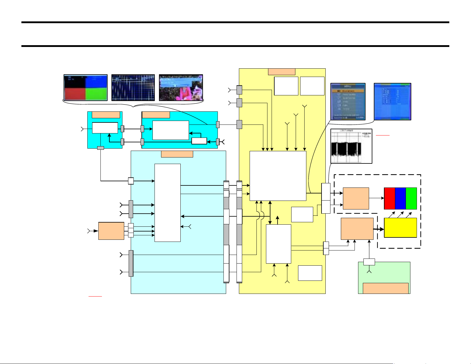
Chapter 4 - Video Processing System
Video 1
Video 3
IC2505
AV
Switcher
Y/C/CV
AU-Board
BU-Bo ard
C
IC5000
Trident
(Video Processor)
Figure 4-1
KDL-26, 32, 40, 46S2000 Video Processing
HDMI
Video 6
Component Input
Video 4
H2-Bo ard
Video 2
RF
I2C-B
IC1001
TV
Micro
A9V
CV
(NTSC)
Y/Pb/Pr
Y/CV
NOTE:
(CV) Composite Video
(Y/CV) Composite & S-Video
(Y) Luminance (brightness) Information S-Video
(C) Chrominance (color) Information S-Video
(Y/Pb/Pr) Analog Component Video
(Y/Cb/Cr) Digital Component Video
Backlight
Invert er
Board
LCD Panel Assemble
Logic
Board
LCD
Panel
Backlights
PC-IN
Video 7
R/G/B
Backlight ON
I2C-A
1 - 4
18V
Panel 5V
CN9000
CN6202
CN7009
CN9501 CN1001
CN5000
16,18
26,28
29
12,14
20,22
24,26
28,30
CV
Y
4
CN9001
CN7501
J9001
J9002
2
6
C
CV
Dimmer
QS-Board
ATI
CPU &
Decoder
RF Tuner
QT-Board
Y/Cb/Cr
(ATSC)
IF
(ATSC)
IC7000
Switching
Regulator
TMDS
G1-Board (26" & 32")
G2-Board (40" & 46")
Switch
I2C
I2C
CN6000
CN4702
Component Input
Video 5
Y/Pb/Pr
I2C-B
10
22
24
8
/
10
/
12
16
/
18
/
20
30
/
32
/
34
38
/
40
/
42
28
26
22
/
23
27
/
28
2.4V
1.8V
D3.3V
STBY
3.3V
1.8V
Information Banner
Service Mode
User Menu
PATN PatternsGPTN Patterns
2
1
NOTE:
Reference
Figures 5-4 & 5-5
for more and enlarged
waveform diagrams
IC1005
User Data
NVM
IC6000
PC-IN
EDID Data
NVM
IC9001
HDMI
EDID Data
NVM
Video System Block Diagram
CTV-38 28
Page 32
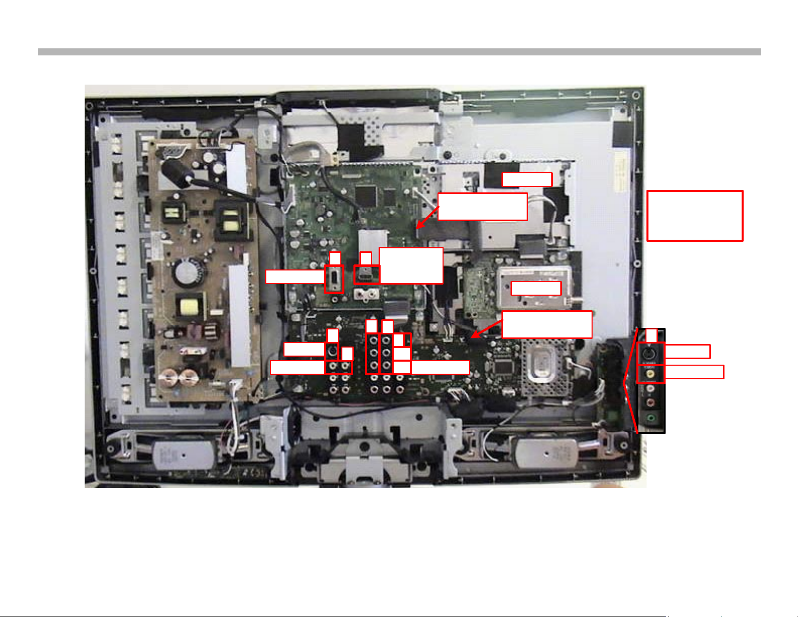
Component Location Diagram
Figure 4-2
KDL-26, 32, 40, 46S2000 Video Input Locations
PC-IN Video
ATSC Video Signal
CN4702
S-Video
Composite
Component
S-Video
Composite
Y
Pb
Pr
1
3
2
4
7
HDMI/DVI
Digital Video
Connector
6
NOTE:
DVI
-to-HDMI
Adaptor is necessary
for DVI Input
5
RF-Tuner
QS-Board
NTSC Video Signal
CN7501
/pin 6
4. Video Processing System
CTV-38 29
Page 33
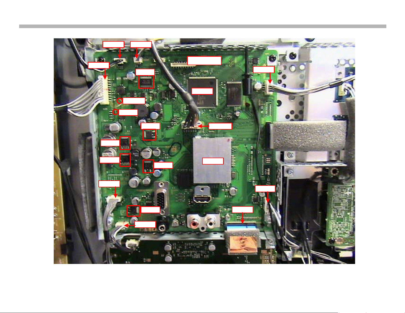
CN1002
CN7009
CN1007
CN1008
CN7008
CN1001
CN4701
IC1001
IC5000
IC7002
IC7001
IC7005
IC7004
IC1010
CN5000
IC1700
BU-Board
IC7000
PS7000
F7000
Figure 4-3
KDL-26, 32, 40, 46S2000 BU-Board Connectors & IC’s Locations
BU-Board Connectors & IC Locations
4. Video Processing System
CTV-38 30
Page 34
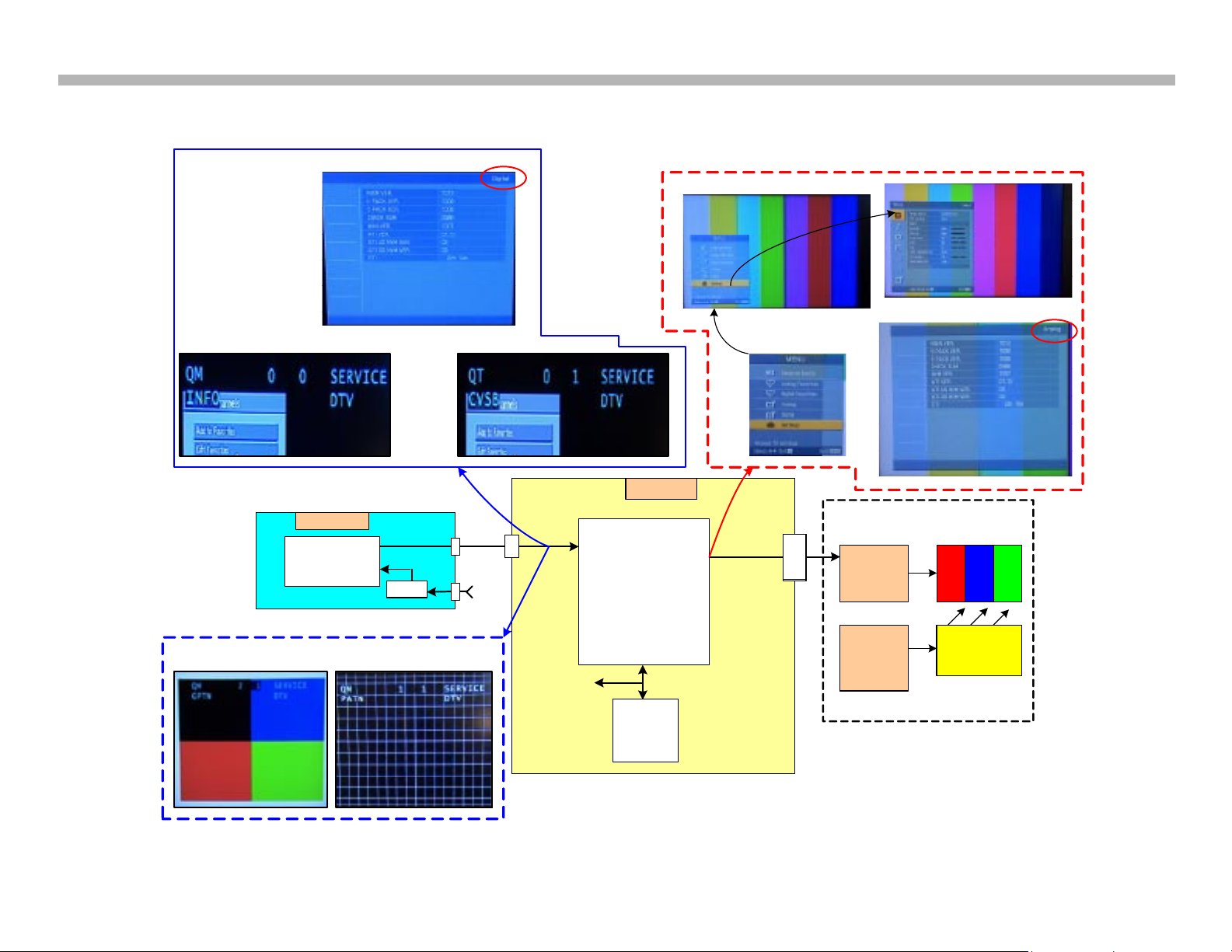
BU-Board
IC5000
Trident
(Video Processor )
I2C
IC1001
Main
Micro
Backlight
Inverter
Board
LCD Panel Assemble
Logic
Board
LCD
Panel
Backlight
CN5000
1,3
5,7
9,11
17,19
Figure 4-4
KDL-26, 32, 40, 46S2000 On-Screen-Displays
QS-Board
ATI
CPU &
Decoder
Y/Cb/Cr
(ATSC)
Switch
I2C
CN4702
I2C-B
QM Service Menu
QT Service Menu
Wega Gate
(User Menu)
Analog Service Mode Display
Digital Service Mode D isplay
ATI Microprocessor & TRIDENT Generated
Main Microprocessor & TRIDENT Generated
QM Internal Patterns
(GPTN )
QM Internal Patterns
(PATN)
I2C-B
On-Screen-Displays (OSD) Diagram
4. Video Processing System
CTV-38 31
Page 35
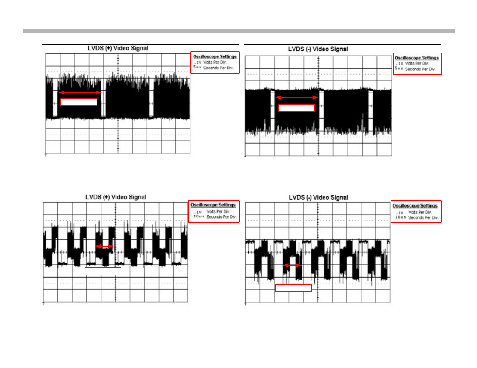
4. Video Processing System
1 Field of Video
1 Field of Video
Figure 5-5
LVDS Vertical Rate
(Complete Fields) Video Signals
Figure
4-5
LVDS Horizontal Rate (Complete Lines) Video Signals
1 Line of Video
1 Line of Video
CTV-38 32
Page 36

4. Video Processing System
Overall System Description
Reference Figures 4-1 and 4-2
The WAX2 chassis models include the following video input sources.
• Composite/S-Video Video 1, 2, 3(Composite Only)
Video 1, 2, 3 are all three-wire cable inputs for composite video with the
Yellow RCA jack transporting all the video information (Synchronization
and Color information) and the Red and White transporting left and
right audio information. The S-Video input uses a single modular jack
with one wire carrying the Y (or luminance information), and the other
wire carrying the C (or chrominance information).
The Composite/S-Video Video 2 is the front panel video jack on the
H2-Board, which uses the same set of cables as just describe in the
previous paragraph. The signal passes through the H2-Board before
being applied to the AU-Board.
Typical external devices are the VCR, DVD, and A/V Receiver units.
• Component Video 4, 5
Video 4 & 5 are both three-wire (Video) cables with a separate twowire (Audio) cable. The three-wire (Red, Green, & Blue) cable
transports the separate Red, Green, and Blue video component video
information. A separate two-wire cable (Red and White) transports
the left and right audio information for each input.
Receiver, and Set-Top-Box units.
• PC-IN Video 7
Video 7 connects directly to a Personal Computer or PC monitor output
source using a HD15 or SVGA cable. The input accepts VGA, SVGA,
XGA, WXGA, and SXGA resolution signals from the PC. A separate
Stereo Mini Plug transports the audio for the PC input.
• RF Input (NTSC & ATSC)
The tuner receives and demodulates all analog CATV (QAM) and Overthe-Air (NTSC & ATSC) broadcast signals. The tuner is mounted on
the QT-Board. All ATSC signal processing circuits are located on the
QS-Board. The composite NTSC signal is applied to the switched on
the AU-Board, and the ATSC signal is applied directly to the TRIDENT
on the BU-Board.
Typical external devices are the DVD, DVR, Satellite Receivers units.
• HDMI/DVI Video 6
Video 5 is a digital video (including audio in the case of HDMI) input
source. The WAX2 chassis models accept both High-Definition
Multimedia Interface or HDMI (Video & Audio) and Digital Visual
Interface or DVI (Video Only) input sources. The DVI connection needs
a DVI-to-HDMI adapter in order to connect to the HDMI connector input.
The BU-Board performs all HDMI/DVI signal processing, including the
digital-to-analog conversion. The analog component signal (Y/Pb/Pr)
is then applied directly to the TRIDENT IC5000.
Typical external devices are the DVD, DVR, Satellite Receivers, A/V
CTV-38 33
Page 37

4. Video Processing System
Video Circuits Functional Description
Reference Figures 4-1 and 4-3
You can divide the Video Processing system into the following three
separate sections.
• Analog Video Switching Section (AU-Board)
• Video Processing Section (BU-Board)
• LCD Drive Circuits Section (LCD Panel Assembly)
The AU-Board receives video inputs 1, 2, 3, and NTSC Signal. The
inputs are output (from switcher IC2505) as one of the following formats
depending on the input.
• Composite CV
• S-Video Y/C
The Component 4 & 5, HDMI/DVI, PC-IN, and ATSC Signal inputs are
applied directly to the TRIDENT on the BU-Board.
The TRIDENT IC5000 contains the following circuits (Wega Engine
circuits), which in previous models where separate integrated circuits.
• Composite Component Processor (CCP)
• Digital Reality Creator (DRC)
IN, and ATSC Signal directly on the BU-Board. The TRIDENT circuitry is
compatible with the VGA, SVGA, XGA, WXGA, and the SXGA formats at
the 60Hz vertical frequency rate. The TRIDENT is compatible with other
vertical frequency rates, however, for the best results select the 60Hz
when ever possible.
The properly scaled TRIDENT output signal on the BU-Board is sent to the
Logic Board on the LCD Panel Assembly. The Logic Board contains the
gamma control circuitry, white balance processing circuitry, and the LCD
drivers, which perform the actual individual pixel control for information
display.
• Scan Converter
The Composite Component Processor (CCP) takes the composite
(CV) signal from the video switcher and converters it to a component (Y/
Pb/Pr).
The Digital Reality Creator (DRC) is a line-doubler and noise-reduction
circuit for the 480i signal. The DRC up-converts the 480i signal to a 1080i
signal (High Definition Format). The DRC acts only as a noise reduction
circuit fir the 1080i signal since it is already in a High Definition format.
The Scan Converter performs the Interlace to Progressive scan
conversion, and performs the signal scaling process to develop a signal
equal to the resolution of the particular size LCD panels
The TRIDENT IC5000 receives the Component 4 & 5, HDMI/DVI, PC-
CTV-38 34
Page 38

4. Video Processing System
Troubleshooting Tips
Reference Figures 4-1, 4-2, and 4-3
When a video problem occurs you will experience one of the two following
symptoms.
• No Video or Distorted Video on All inputs
• No Video or Distorted Video on a Select Number of Inputs
The main objective when troubleshooting one of the previously listed
symptoms is to determine if the defective exists in the LCD Panel Assembly
(Display), Backlight Inverter Board, BU-Board (Video Processing), or G1/
G2-Board (Power Supply System).
No Video or Distorted Video Troubleshooting
The first step when a “No Video or Distorted Video” failure occurs is to
determine if the video anomaly is on all video input sources, or if it is only
on one or a select number of video input sources. The answer to this
question will provide a strong clue to whether the failure is occurring in a
circuit common to all inputs, or in a circuit associated with only a single
or a select number of inputs. Furthermore, is a defective external device
causing the problem?
Is video missing or distorted on all video inputs? Is the Standby-LED
Flashing Red or the Power-LED glowing Steady Green? In other words,
is the unit shutting down and going into a particular protection mode?
When the Power-LED is flashing Red a protection circuit has detected an
error and the Main Microprocessor is shutting the unit OFF and placing it
into a particular protection mode. In this case, you should go to one of the
Protection Mode Troubleshooting.
TRIDENT video processor and the ATI microprocessor. On-ScreenDisplays (OSD’s) are very usefully in troubleshooting a video problem.
Attempting to display the OSD will quickly isolates video system anomalies
to either the BU-Board (video processing circuitry) or the LCD Panel
Assembly (display circuitry). For example, the TV you are working on
exhibits a “No Video” condition on all Inputs, however, the “User Menu”
does display, then the LCD Panel Assembly is working properly and the
defective component is on the BU-Board. Replace the BU-Board.
If the “User Menu” does not display, check the connections (CN5000 to the
LCD Panel Assembly) between the BU-Board and the LCD Panel Assembly
before proceeding any further. Secure and/or repair connections, and
recheck video display.
If after securing and/or repairing the connections the video anomaly
remains, check the LVDS video waveforms on CN5000/pins 1 – 19 (odd
pins). Reference waveform diagrams in Figures 4-4 & 4-5 for proper
waveform displays.
If the waveforms are present at CN5000, then the video processing circuits
(TRIDENT) on the BU-Board are functioning properly, and the problem
exists on the LCD Panel Assembly.
If however, the waveforms are not present at CN5000, then the video
processing circuits (TRIDENT) on the BU-Board are defective and the
BU-Board must be replaced.
If the “No Video” condition persists after securing and/or repairing the
connections and confirming video waveform, then you should turn your
attention to troubleshooting a power supply failure. Check the 10.5V at
CN6202/CN6200/pin 7.
If the 10.5V is present replace the BU-Board.
If the Power-LED is not flashing Red, but instead, the Power-LED glows
a steady Green then the next step is to attempt to display the User Menu
also know as On-Screen-Display (or OSD).
On-Screen Displays (OSD)
• User Menu
• Service Mode
• Information Banner
Figure 4-1 shows the location of the OSD generators, which are the
If the 10.5V is missing go to the details on troubleshooting a power supply
problem.
Video Input Troubleshooting
The primary objective here is to locate the defective component through
testing the individual video inputs.
CTV-38 35
Page 39

4. Video Processing System
When the video anomaly appears on only one or two video inputs then
the next step is to eliminate the possibility of a defective or improperly
connected external device such as, a VCR or DVD player. The quickest
way to troubleshoot the external devices is to substitute a known good
device with the suspect device at the particular input.
If the external device or connections are defective then the TV is OK. In
this case, service and/or repair external device or connections to the TV
inputs.
If the external devices and their connections are OK, then the next step
is to troubleshoot the problem by accessing and displaying each video
input.
The rationale behind this troubleshooting method is that each of these
video inputs take an altogether or somewhat unique path through the
video processing system. This fact enables you to determine the defect, in
some cases, down to the component level, and in almost all cases, down
to at least the board level. For example, if the video anomaly appears
in Video inputs 1 and 3, however, if does not appear in the HDMI input,
then the defect exists on the AU-Board. The reason for this conclusion
is that although all these inputs (HDMI and Video1 & 3) pass through
the TRIDENT on the BU-Board, the AU-Board is unique to the Video
1 & 3 signal path. Therefore, the AU-Board is the only component that
can exclusively affect these inputs, while not affect the HDMI input.
Troubleshoot the AU-Board.
When troubleshooting a “No Video” condition in the RF Tuner mode
the Digital/Analog channel selection feature on the remote controller can
be used to isolate the problem area. This is true because the digital signal
(or channel) processing is performed on the QS-Board, and the analog
signal (or channel) processing is performed on the QT-Board.
If analog channels are received, but no digital channels replace the QSBoard.
If digital channels are received, but no analog channels replace the QTBoard.
If both the analog and digital channels are not received, check for 10.5V
at CN4701/pin 3. This is the supply voltage for the QS-Board. Replace
the QS-Board if the 10.5V is present at CN4701.
If the 10.5V is not present at CN4701, the next step is to check for 18.5V
at cn6202/CN6200/pin 13. This will discern a problem between the power
supply and the BU-Board regulators.
Replace the BU-Board if the 18.5V is present at CN4701.
Replace the G1/G2-Board if the 18.5V is missing at CN4701.
The opposite of the previous conclusion is true if the video anomaly
appears on the HDMI input, but not on the Video 1 & 3 inputs. In this
case the failure would exist on the BU-Board. HDMI input are directly
connected to the video switcher on the BU-Board. In this case, the failure
exists on the BU-Board. Replace the BU-Board.
You can apply the same deductive reasoning when troubleshooting video
anomalies using the other video inputs. This method simply involves
knowing the complete video path the input signal takes from the input,
through the video processing system, and finally to the display. With this
knowledge you can effectively divide the video system into distinct areas,
and therefore, isolate the defect.
CTV-38 36
Page 40
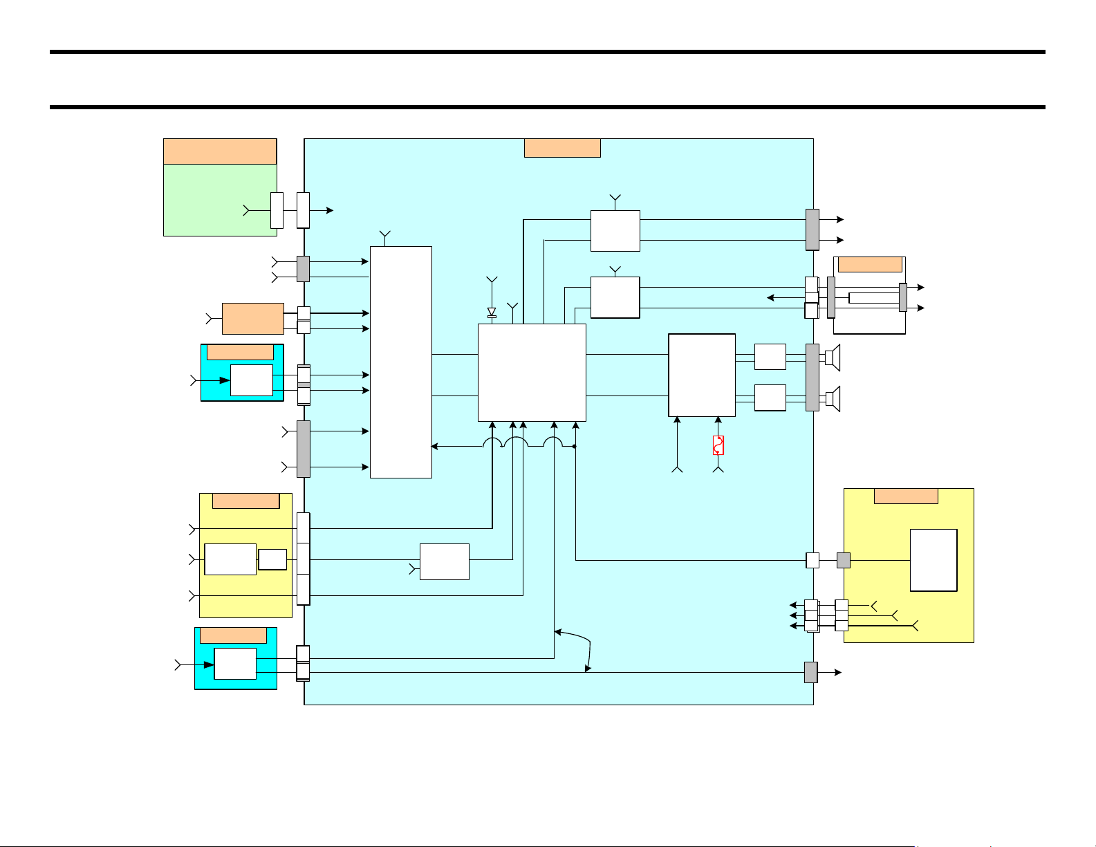
Chapter 5 - Audio Processing System
Video (audio) 1
Video
(audio) 3
IC2001
Audio
Switcher
L/R
AU-Board
DVI Audio
Input
Component Audio Input
Video
4
H2-Board
Video 2
NTSC
Tuner
RF
QT-Board
J9003
Figure 5-1
KDL-26, 32, 40, 46S2000 Audio Processing
L/R
L
L/R
R
IC7001
Audio
DSP
IC7007
Digital
Amplifier
H2-Board
L
R
Headphone
Output
Variable/Fixed Audio
Output
L
R
R
L
BU-Board
IC1001
Main
Micro
I2C-A
30
CN9001
CN9501
CN1001
J9852
CN9851
A9V
D5V
PS7754
CN7000
1
/
2
A9V
A15VA15V
3
1
9
7
R
L
R
CN9001
CN7501
CN9501
J9001
J9002
PC-IN
Audio Input
Video
7
HP Switch
3HP-Det to Main Micro
BU-Board
L
LPF
LPF
2
1
ATI
Micro
QS-Board
J9003
Optical Audio
Output
IF from
QT-Board
CN7502
ATSC Tuner
Digital Audio
Component Audio Input
Video
5
L/R
I2S
SPDIF
IC5000
TRIDENT
D/A
HDMI
Video
6
HDMI Audio
L/R
L/R
A9V
CN9502
CN7503
A15V
I2C-A
I2C-B
IC7003
OP
-AMP
IC7601
OP
-AMP
IC7602
OP
-AMP
A9V
A9V
A9V
A9V
D7005
PWM
-L
PWM
-R
A9V
D5V
3
4
1
3
4
1
D5V
D3.3V
1
/
2
43
/
45
39
/
41
47
/
49
D3.3V
G1-Board (26" & 32")
G2-Board (40" & 46")
3
1
CN7008
CN6202
CN6200
Audio System Block Diagram
CTV-38 37
Page 41
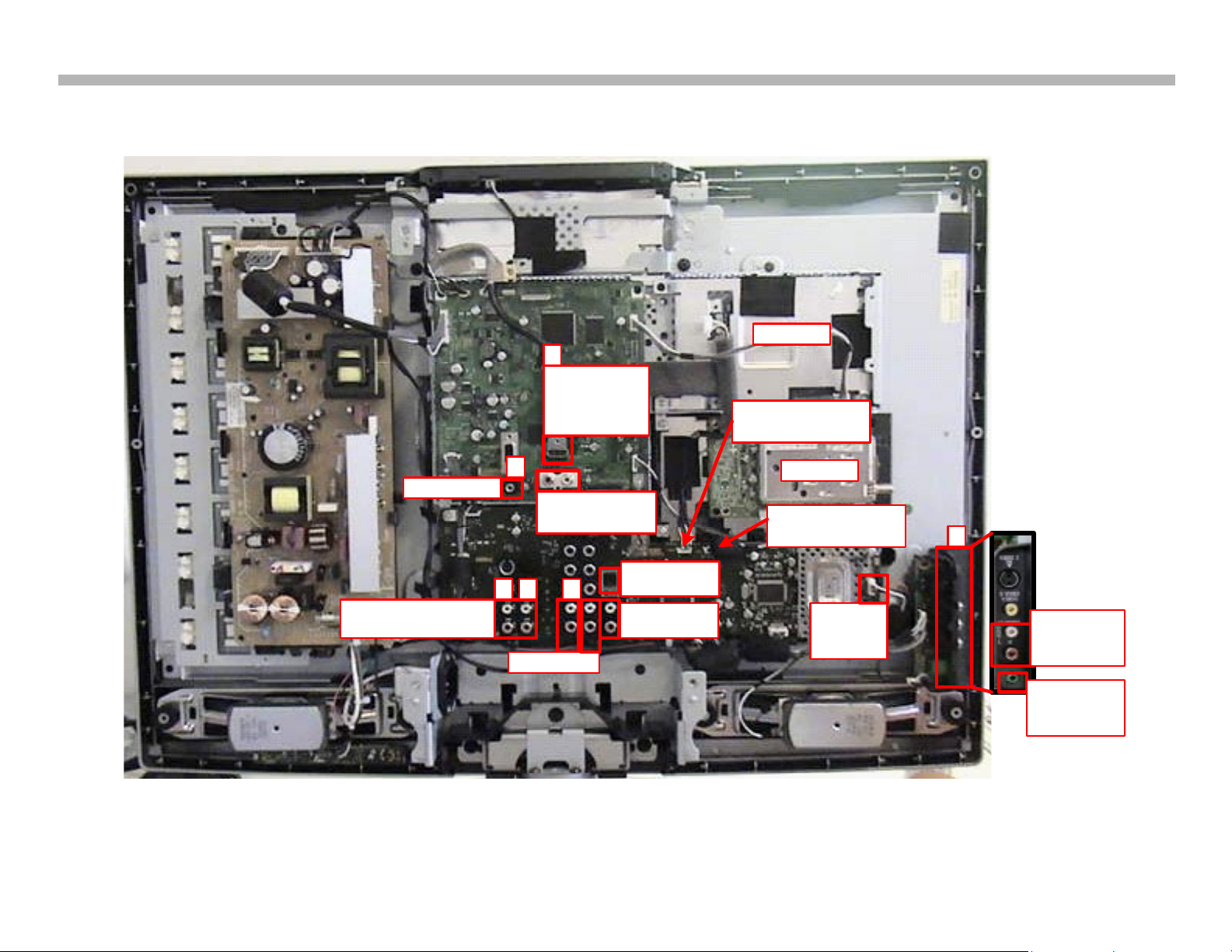
Component Location Diagram
Figure 5-2
KDL-26, 32, 40, 46S2000 Audio Input Locations
ATSC Video Signal
CN7502
/pin 1 & 3
RF-Tuner
QS-Board
NTSC Audio Signal
CN7501/pin 1 & 3
PC-IN Audio
Var/Fix
Audio Output
Component
S-Video & Composite
Audio Input
2
S-Video &
Composite
Audio Input
Headphone
Audio Output
Connector
1
3
4
5
6
DVI
Audio Connector
HDMI
Digital
Video & Audio
Connector
Speaker
Outputs
CN7000
Optical Audio
Output
5. Audio Processing System
CTV-38 38
Page 42
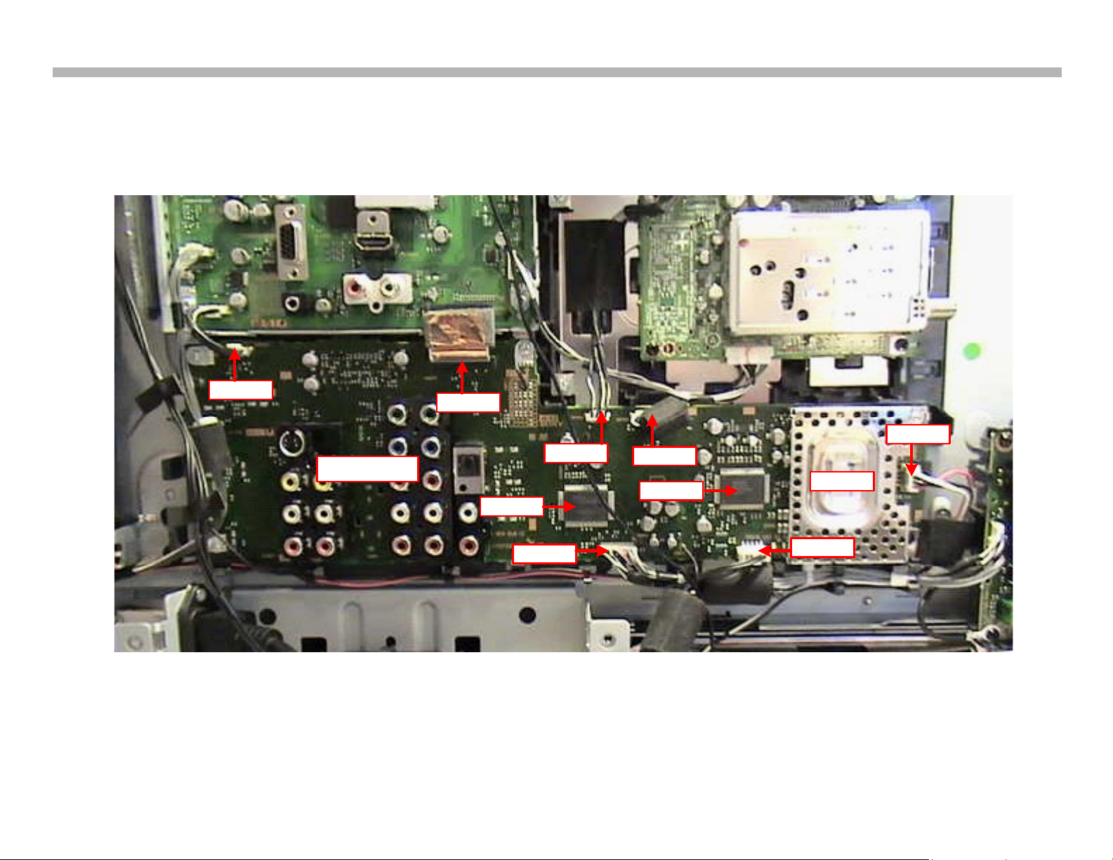
5. Audio Processing System
CN9501
Figure 5-3
KDL-26, 32, 40, 46S2000 AU-Board Connectors & IC’s Locations
CN7503
CN9001
CN9502
CN7501
CN7502
IC2001
IC7001
IC7007
CN7000
AU-Board
CTV-38 39
Page 43

5. Audio Processing System
Overall System Description
Reference Figures 5-1, 5-2, & 5-3
Audio inputs 1, 3, 4, and 5 are routed directly to IC2001 (Analog Audio
Switch) on the AU-Board. The only audio inputs not applied directly to
the IC2001 on the AU-Board are as follows. These inputs all have unique
interface boards connected between the input and the AU-Board.
• Audio Input 2
• NTSC Tuner
Audio Input 2 mounts to the H2- Board, which connects to the AU-Board
at CN9001.
The NTSC Tuner mounts to the QT-Board, which connects to the AUBoard at CN7501.
The following audio inputs are routed directly to the DSP IC7001 on the
AU-Board.
• HDMI
• DVI
• PC-IN
• ATSC Tuner
The HDMI input connector (modular jack) mounts directly to the BUBoard. The HDMI audio signal is processed by the TRIDENT, and the
audio signal is connected to the AU-Board at CN9501.
The DVI input connector (RCA jacks) mounts directly to the BU-Board.
The DVI audio signal passes through the BU-Board, and the audio signal
is connected to the AU-Board at CN9501.
The PC-IN input connector (Mini-Phone jack) mounts directly to the BUBoard. The PC-IN audio signal passes through the BU-Board, and the
audio signal is connected to the AU-Board at CN9501.
The digital ATSC tuner audio signal is processed on the QS-Board. The
digital audio outputs are connected to the AU-Board at CN7502. The I2S
signal is used for the internal audio processing in the DSP IC7001. The
SPDIF signal is used for external audio processing at the Optical Audio
Output J9003.
The audio processing system in the WAX2 chassis is a completely digital
audio processing and amplifying system. The single output of the analog
switcher IC2001 is applied to the DSP where it is digitized.
The DSP IC7001 disperses audio to the following outputs.
• Digital Audio Amplified IC7007 (digital audio signal)
• Headphone Audio Amplifier IC7602(analog audio signal)
• Variable/Fixed Audio Amplifier IC7601 (analog audio signal)
The DSP IC7001, which is controlled by the Main Microprocessor over the
I2C-A bus (at CN9501/pin 30) performs all audio adjustments and effects,
such as those listed in the following bullet list.
• Volume
• Sound Mode (Dynamic, Natural, and Clear Voice)
• Treble
• Bass
• Balance
• Steady Sound
• Surround
• BBE
• MTS (Stereo, Auto SAP, and Mono)
• Variable/Fixed Switching
• Speaker/Headphone Switching
The main audio amplifier is an S-Master digital audio amplifier. The
analog audio from the switcher IC2001 is converted to a Pulse Width
Modulated (PWM) signal, which is then applied to the Digital Amplifier
IC7007. The Digital Amplifier will adjust the pulse width depending on the
volume control setting. The adjusted PWM signal is then applied to the
Low-Pass Filter (LPF), where the digital high frequency components are
filtered out and the resultant analog signal is applied to the speakers.
CTV-38 40
Page 44

5. Audio Processing System
Troubleshooting Tips
Reference Figures 5-1, 5-2, & 5-3
The first step when a “Missing or Distorted Audio” defect occurs is to
determine if audio is missing on all audio input sources, or if there is
missing or distorted audio on a single or a select number of audio input
sources.
Let us first consider the case in which the audio anomaly is present on
all audio inputs. Although in most cases this is a strong indication of
a defective AU-Board, you should first eliminate the possibility of poor
connections and/or defective speaker. First check the Headphone audio
output.
If the audio anomaly is present at the Headphone output, on all inputs,
then this is a clear indicator of a failure of the Switcher IC2001 and/or the
DSP IC7001 on the AU-Board. This check at the same time eliminates
a possible failure of the speakers because the audio anomaly is also
present at the DSP output.
Before replacing the AU-Board check for the A9V supply voltage at
CN9502/pin 1.
If the A9V is present at CN9502/pin1 replace the AU-Board.
If the A9V is missing at CN9502/pin 1 a failure in the power supply has
occurred. Replace the G1/G2-Board.
Check the external devices and their associated cables connected to the
faulty input(s) first.
Substitute (or Swap) known good devices and cables on the faulty
input. First substitute the cable and then the device if necessary to
determine if the device or cable is causing the problem. Replace the
cable or have the device repaired if found to be defective. However, if the
external device and cable is OK, then the next step is to test the unique
board or module associated with the separate input sources.
For example, consider an audio anomaly found on Video 2, however, Video
1, 3, 4, and 5 checks OK. Because all these inputs are applied to the same
switcher IC2001 on the AU-Board, you must locate a component unique
to the Video 2 input that could be causing the anomaly. In this case, the
H2-Board is unique to the Video 2 input, and is the only component that
will cause a problem on Video 2 and not affect Video 1, 3, 4, and 5 inputs.
Replace the H2-Board.
Another example would be missing or distorted audio on the HDMI (Video
6) input only. However, the PC-IN is OK. The only board that would affect
only the HDMI audio input is the BU-Board (specifically the TRIDENT).
The PC-IN passes through the BU-Board with no processing. Therefore,
replacing the BU-Board should fix this problem.
When the audio anomaly is not present at the Headphone audio output,
then this indicates a properly functioning DSP IC7001 and all preceding
circuits. In this case, you must perform further checks to determine if the
failure exists on the AU-Board or with the speakers. Check the speaker
connections and speaker resistance.
If the connection at CN7000 and the speaker wires and clips check OK
and the speaker resistance measure 8 ohms, then this indicates a failure
of the Digital Amplifier IC7007. Replace the AU-Board. On the other hand,
if you find the connections or speakers loose or damaged, repair and/or
replace the defective components, and recheck audio output.
Let us now go back and consider the case in which only a single audio
input or select number of audio inputs are experiencing a problem.
CTV-38 41
Page 45
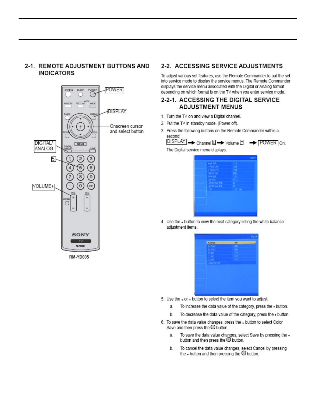
Service Mode Options
Acessing Service Adjustments
Appendix
1
Page 46
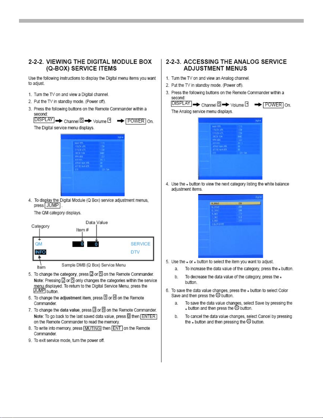
Acessing Digital & Analog Service
CTV-38 Appendix
2
Page 47
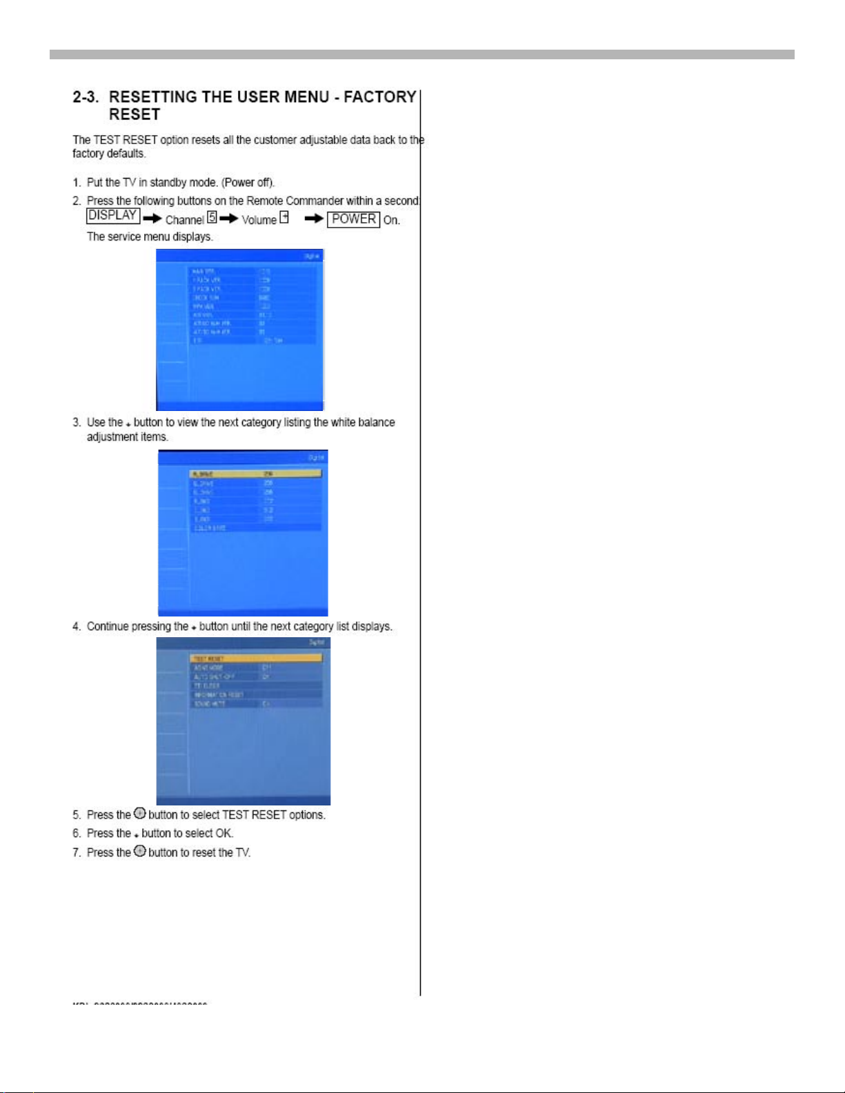
Factory Reset
CTV-38 Appendix
3
Page 48
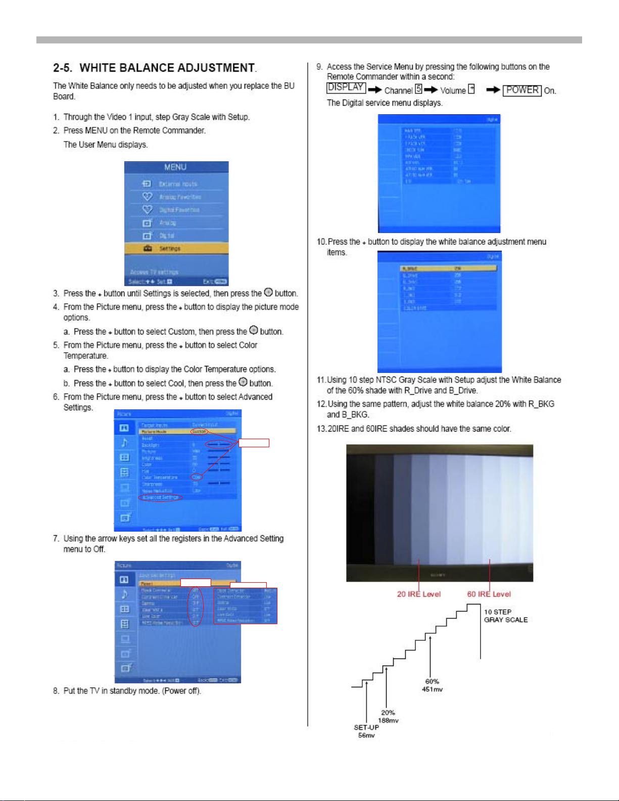
White Balance
Adjustment Settings
Typical Factory Sett ings
White Balance
Adjustment Settings
White Balance Adjustment
CTV-38 Appendix
4
Page 49
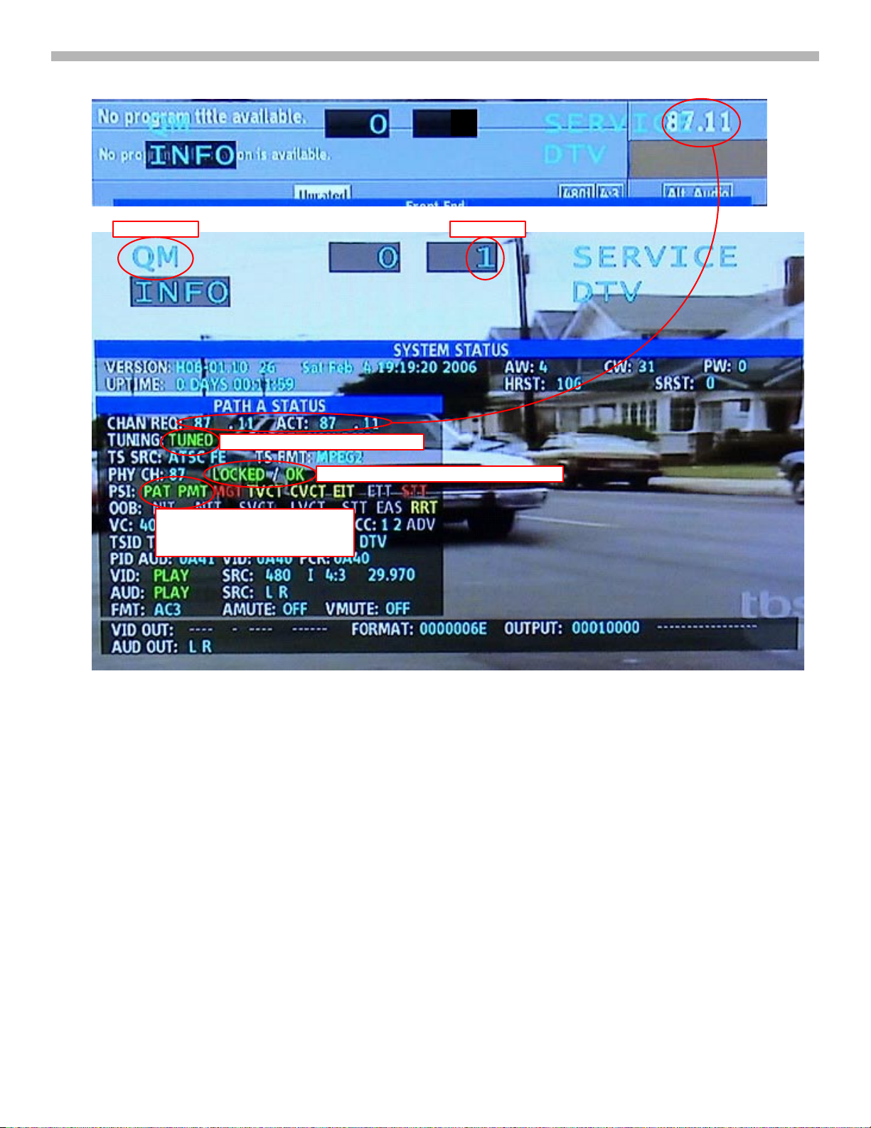
Digital Channel Information & Status
QM Catagory
Data Value
Tuner Locked to Channel Frequency
MPEG Decoder Locked to Transport Stream
Program Association Table (PAT)
Program Management Table
(PMT)
Must Be Green
1
System Status
CTV-38 Appendix
1) Set TV to Service Mode: Press the following button in the shown sequence.
DISPLAY - 5 - Volume + - POWER
2) Press the “Jump” button once
3) Press the “3” button once
NOTE: All indicated items must be in the GREEN status. If any items are itermintently changing to
YELLOW or in a steady RED state, then the video will intermintently display or not display at all.
Troubleshooting:
1) Check Analog channels
If analog channels are displayed in good quality, then is indicates a good physical cable connection.
If the analog are poorly displayed check physical cable connection.
2) Check other digital channels
If the anomily is only occuring on a single channel, then this indicates a Cable Provide fault. That particular channel is not bring transmitter properly.
If all digital channels exhibit the anomily this indocates a possble Q-Box fault. However, before replacing the Q-Box confirm that physical cable coonection. Furthermore, contact the Cable Provide to
confirm no channel transmission problem on their end.
5
Page 50
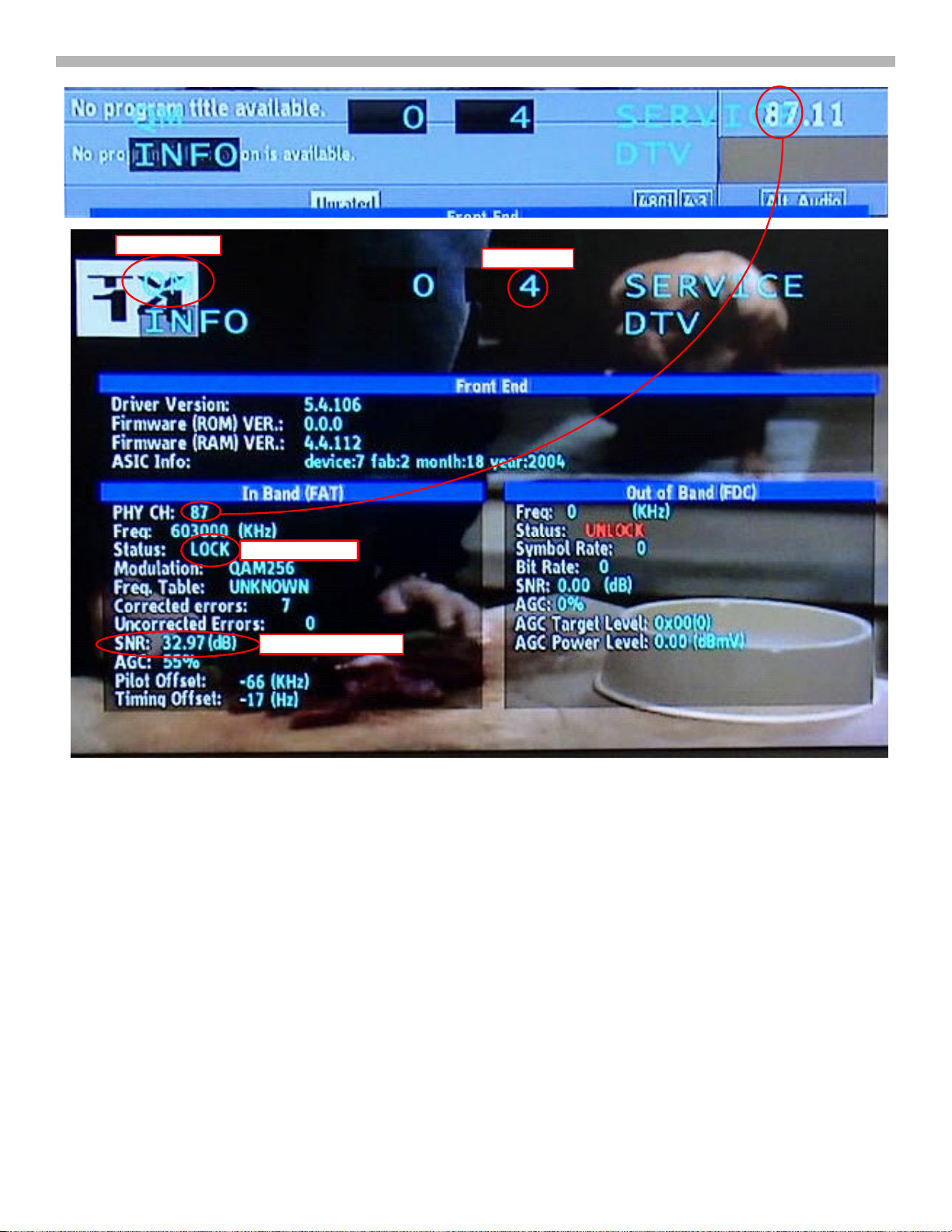
QM Catagory
Data Value
Channel Locked
Greater Than 30dB
Front End Status
CTV-38 Appendix
1) Set TV to Service Mode: Press the following button in the shown sequence.
DISPLAY - 5 - Volume + - POWER
2) Press the “Jump” button once
3) Press the “3” button four times
Troubleshooting:
1) Check Analog channels
A poor physical cable connection will cause a poor SNR reading (approaching 30dB).
If analog channels are displayed in good quality, then is indicates a good physical cable connection.
If the analog are poorly displayed check physical cable connection.
2) Check other digital channels
If the anomily is only occuring on a single channel, then this indicates a Cable Provide fault. That particular channel is not bring transmitter properly.
If all digital channels exhibit the anomily this indocates a possble Q-Box fault. However, before replacing the Q-Box confirm that physical cable coonection. Furthermore, contact the Cable Provide to
confirm no channel transmission problem on their end.
6
Page 51
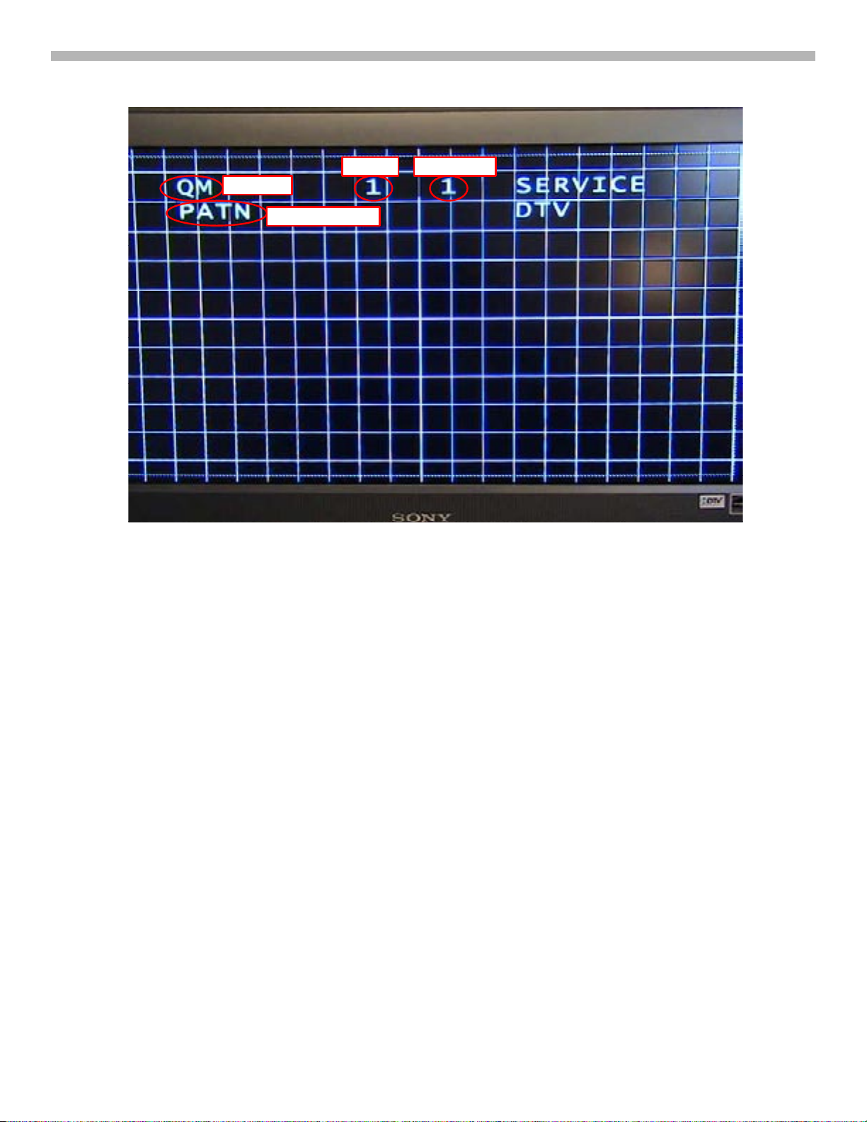
Internal Pattern Genera-
Catagory
Item Description
Item #
Data Value
PATN
CTV-38 Appendix
1) Set TV to Service Mode: Press the following button in the shown sequence.
DISPLAY - 5 - Volume + - POWER
2) Press the “Jump” button once
3) Press the “1” button once (the “1” & “2” buttons change the Item Discription & Item # simultaneously)
4) Press the “3” & “4” button to scroll up or down throught the various patterns (Data Value)
NOTE: the “2” & “5” buttons change the Catagory
Pattern Format List:
Data Value 1 -20: 1080i
Data Value 21 -40: 480i
Data Value 41 -60: 480p
Data Value 61 -80: 720p
7
Page 52
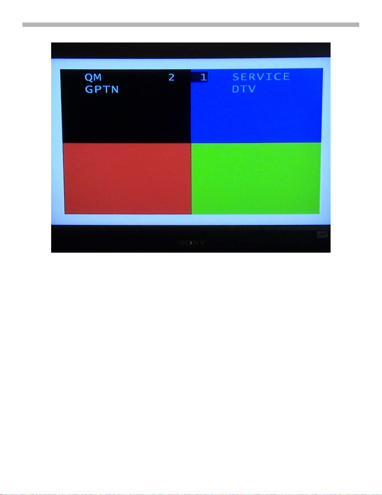
GPTN
CTV-38 Appendix
1) Set TV to Service Mode: Press the following button in the shown sequence.
DISPLAY - 5 - Volume + - POWER
2) Press the “Jump” button once
3) Press the “1” button twice (the “1” & “2” buttons change the Item Discription & Item # simultaneously)
4) Press the “3” & “4” button to scroll up or down throught the various patterns (Data Value)
NOTE: the “2” & “5” buttons change the Catagory
Pattern Format List:
Data Values 1 - 12 : 480i
8
Page 53
and i.Link are trademarks of Sony Electronics
2006 Sony Electronics, Inc.
EMCSA - A Service Company
1 Sony Drive
Park Ridge, New Jersey 07656
CTV380531 02/11/07
Reproduction in whole or part without written permission is prohibited. All rights reserved
 Loading...