

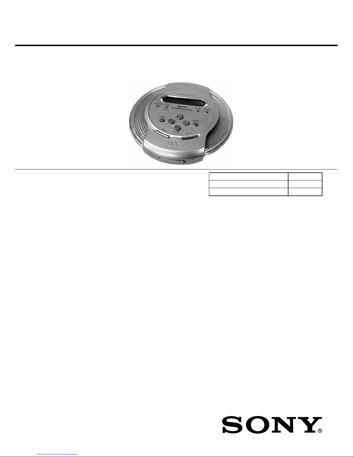
Sony Walkman D-CJ01 Service Manual
Ver 1.1 2002.01
9-873-390-02
2002A0200-1
© 2002.1
Sony Corporation
Personal Audio Company
Published by Sony Engineering Corporation
SERVICE MANUAL
PORTABLE CD PLAYER
US Model
Canadian Model
AEP Model
UK Model
E Model
Australian Model
Chinese Model
Tourist Model
Model Name Using Similar Mechanism D-EJ621
CD Mechanism Type CDM-3123EBA
Optical Pick-up Type DAX-23E
SPECIFICATIONS
D-CJ01
– Continued on page 2 –
System
Compact disc digital audio system
Laser diode properties
Material: GaAlAs
Wavelength: λ = 780 nm
Emission duration: Continuous
Laser output: Less than 44.6 µW
(This output is the value measured at a distance
of 200 mm from the objective lens surface on
the optical pick-up block with 7 mm aperture.)
D-A conversion
1-bit quartz time-axis control
Frequency response
20 - 20 000 Hz +1dB (measured by JEITA CP-307)
Output (at 4.5 V input level)
Line output (stereo minijack)
Output level 0.7 V rms at 47 k Ω
Recommended load impedance over 10 k Ω
Headphones (stereo minijack)
Approx.5 mW + Approx. 5 mW at 16 Ω
Power requirements
For the area code of the model you
purchased, check the upper left side of the
bar code on the package.
• Two Sony NC-WMAA rechargeable
batteries: 2.4 V DC
• Sony NH-WM2AA rechargeable batteries:
2.4 V DC
• Two LR6 (size AA) batteries: 3 V DC
• AC power adaptor (DC IN 4.5 V jack):
US / Canadian / C&SA model:
120 V, 60 Hz
AEP / French / EE / E13 model:
220 - 230 V, 50/60 Hz
UK model: 230 - 240 V, 50 Hz
Australian model: 240 V, 50 Hz
Korean model: 100 - 240 V,
50/60 Hz
Hong Kong model: 220 V, 50/60 Hz
Chinese model: 220 V, 50 Hz
Tourist model: 100-240V, 50/60Hz
–2

2
D-CJ01
Specifications ............................................................................ 1
1. SERVICING NOTES................................................... 3
2. GENERAL
Locating the Controls......................................................... 4
3. DISASSEMBLY
3-1. Cabinet (Lower) Sub ASSY,
Cabinet (Inner) Sub ASSY ......................................... 5
3-2. MD Mechanism .......................................................... 5
3-3. Main Board ................................................................. 6
3-4. “Motor ASSY, Turn Table (Spindle) (M901)”............ 6
3-5. “Motor ASSY (Sled) (M902)”,
Optical Pick-up (DAX-23E) ...................................... 6
3-6. Switch Unit ................................................................. 7
4. ELECTRICAL ADJUSTMENTS ............................. 8
5. DIAGRAMS
5-1. Explanation of IC Terminals....................................... 9
5-2. Block Diagram(1/2) ...................................................11
5-3. Block Diagram(2/2) .................................................. 12
5-4. Printed Wiring Boards – Main Board (Side A) –...... 13
5-5. Printed Wiring Boards – Main Board (Side B) –...... 14
5-6. Schematic Diagram – Main Section (1/4) – ............. 15
5-7. Schematic Diagram – Main Section (2/4) – ............. 16
5-8. Schematic Diagram – Main Section (3/4) – ............. 17
5-9. Schematic Diagram – Main Section (4/4) – ............. 18
6. EXPLODED VIEWS
6-1. Upper Lid Section..................................................... 22
6-2. Main Section............................................................. 23
6-3. Optical pick-up Section (CDM-3123EBA) .............. 24
7. ELECTRICAL PAR TS LIST................................... 25
SAFETY-RELATED COMPONENT WARNING!!
COMPONENTS IDENTIFIED BY MARK 0 OR DOTTED LINE
WITH MARK 0 ON THE SCHEMATIC DIAGRAMS AND IN THE
PARTS LIST ARE CRITICAL TO SAFE OPERATION.
REPLACE THESE COMPONENTS WITH SONY PARTS WHOSE
PART NUMBERS APPEAR AS SHOWN IN THIS MANUAL OR IN
SUPPLEMENTS PUBLISHED BY SONY.
Flexible Circuit Board Repairing
• Keep the temperature of the soldering iron around 270°C during
repairing.
• Do not touch the soldering iron on the same conductor of the
circuit board (within 3 times).
• Be careful not to apply force on the conductor when soldering or
unsoldering.
Notes on chip component replacement
• Never reuse a disconnected chip component.
• Notice that the minus side of a tantalum capacitor may be damaged by heat.
TABLE OF CONTENTS
CAUTION
Use of controls or adjustments or performance of procedures other
than those specified herein may result in hazardous radiation
exposure.
DANGER
Invisible laser radiation when open and interlock failed or defeated.
Avoid direct exposure to beam.
Battery life* (approx. hours)
(When you use the CD player on a flat and stable surface.)
Playing time varies depending on how the CD player is used.
Figures in brackets show the playing time of
MP3 files.
When using G-PROTECTION function
“1” “2”
Two NC-WMAA 10.5 10.5
(charged for [8] [8]
about 3 hours**)
NH-WM2AA 22.5 23
(charged for [18] [18]
about 5 hours**)
Two Sony alkaline 31.5 32
batteries LR6(SG) [24] [24]
(produced in Japan)
* Measured value by the standard of JEITA (Japan
Electronics and Information Technology
Industries Association).
** Charging time varies depending on how the
rechargeable battery is used.
Operating temperature
5°C - 35°C (41°F - 95°F)
Dimensions (w/h/d) (excluding
projecting parts and controls)
Approx. 132.0 × 29.9 × 137.5 mm
(5 1⁄4 × 1 3⁄16 × 5 1⁄2 in.)
Mass (excluding accessories)
Approx. 218 g (7.7 oz.)
Design and specifications are subject to change
without notice.
• Abbreviation
EE : East European
C&SA : Central & SouthAmerica
ATTENTION AU COMPOSANT AYANT RAPPORT
À LA SÉCURITÉ!!
LES COMPOSANTS IDENTIFIÉS PAR UNE MARQUE 0 SUR
LES DIAGRAMMES SCHÉMATIQUES ET LA LISTE DES
PIÈCES SONT CRITIQUES POUR LA SÉCURITÉ DE
FONCTIONNEMENT. NE REMPLACER CES COMPOSANTS
QUE PAR DES PIÈCES SONY DONT LES NUMÉROS SONT
DONNÉS DANS CE MANUEL OU DANS LES SUPPLÉMENTS
PUBLIÉS P AR SONY.
3
D-CJ01
The laser diode in the optical pick-up block may suffer electrostatic
breakdown because of the potential difference generated by the charged
electrostatic load, etc. on clothing and the human body. During repair,
pay attention to electrostatic breakdown and also use the procedure in
the printed matter which is included in the repair parts.
The flexible board is easily damaged and should be handled with care.
NOTES ON LASER DIODE EMISSION CHECK
The laser beam on this model is concentrated so as to be focused on the
disc reflective surface by the objective lens in the optical pick-up block.
Therefore, when checking the laser diode emission, observe from more
than 30cm away from the objective lens.
Before Replacing the Optical pick-up Block
Please be sure to check thoroughly the parameters as per the “Optical
pick-up Block Checking Procedure” (Part No. : 9-960-027-11) issued
separately before replacing the optical Pick-up block.
Note and specifications required to check are given below.
• FOK output : IC601 eg pin
When checking FOK, remove the lead wire to disc motor.
• RF signal P-to-P value : 0.4 to 0.8Vp-p
USABLE FORMAT
Use ISO9660 Level 1 format
SECTION 1
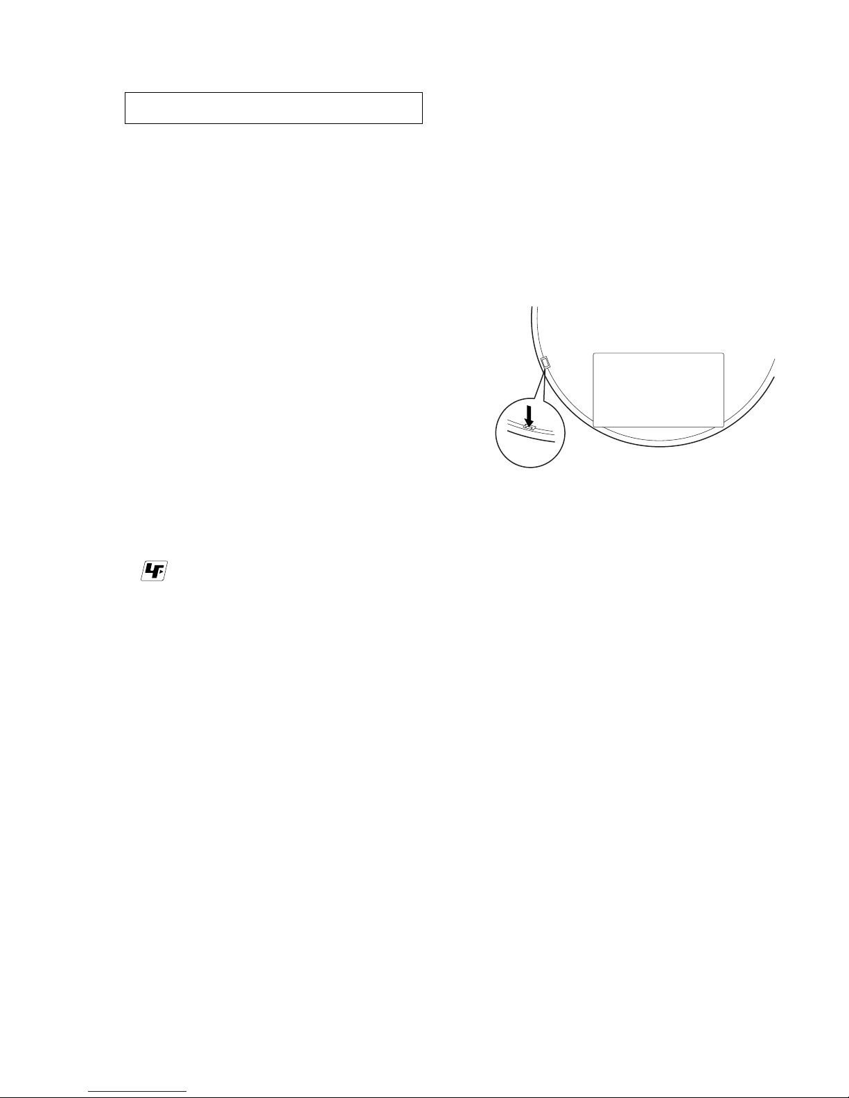
SERVICING NOTES
Laser Diode Checking Methods
During normal operation of the equipment, emission of the laser diode
is prohibited unless the upper panel is closed while turning ON the S801
(push switch type).
The following checking method for the laser diode are operable.
Method :
Emission of the laser diode is visually checked.
1. Open the upper lid.
2. Push the S801 as shown in Fig. 1.
3. Check the object lens for confirming normal emission of the laser
diode. If not emitting, there is a trouble in the automatic power
control circuit or the optical pick-up. During normal operation, the
laser diode is turned ON about 2.5 seconds for focus searching.
NOTES ON HANDLING THE OPTICAL PICK-UP BLOCK OR
BASE UNIT
Fig.1 Method to push S801
S801
z
UNLEADED SOLDER
Boards requiring use of unleaded solder are printed with the
lead-free mark (LF) indicating the solder contains no lead.
(Caution: Some printed circuit boards may not come printed
with the lead free mark due to their particular size.)
: LEAD FREE MARK
Unleaded solder has the following characteristics.
• Unleaded solder melts at a temperature about 40°C higher
than ordinary solder.
Ordinary soldering irons can be used but the iron tip has to
be applied to the solder joint for a slightly longer time.
Soldering irons using a temperature regulator should be set
to about 350°C.
Caution: The printed pattern (copper foil) may peel away if
the heated tip is applied for too long, so be careful!
• Strong viscosity
Unleaded solder is more viscous (sticky, less prone to
flow) than ordinary solder so use caution not to let solder
bridges occur such as on IC pins, etc.
• Usable with ordinary solder
It is best to use only unleaded solder but unleaded solder
may also be added to ordinary solder.
4
D-CJ01
SECTION 2
GENERAL
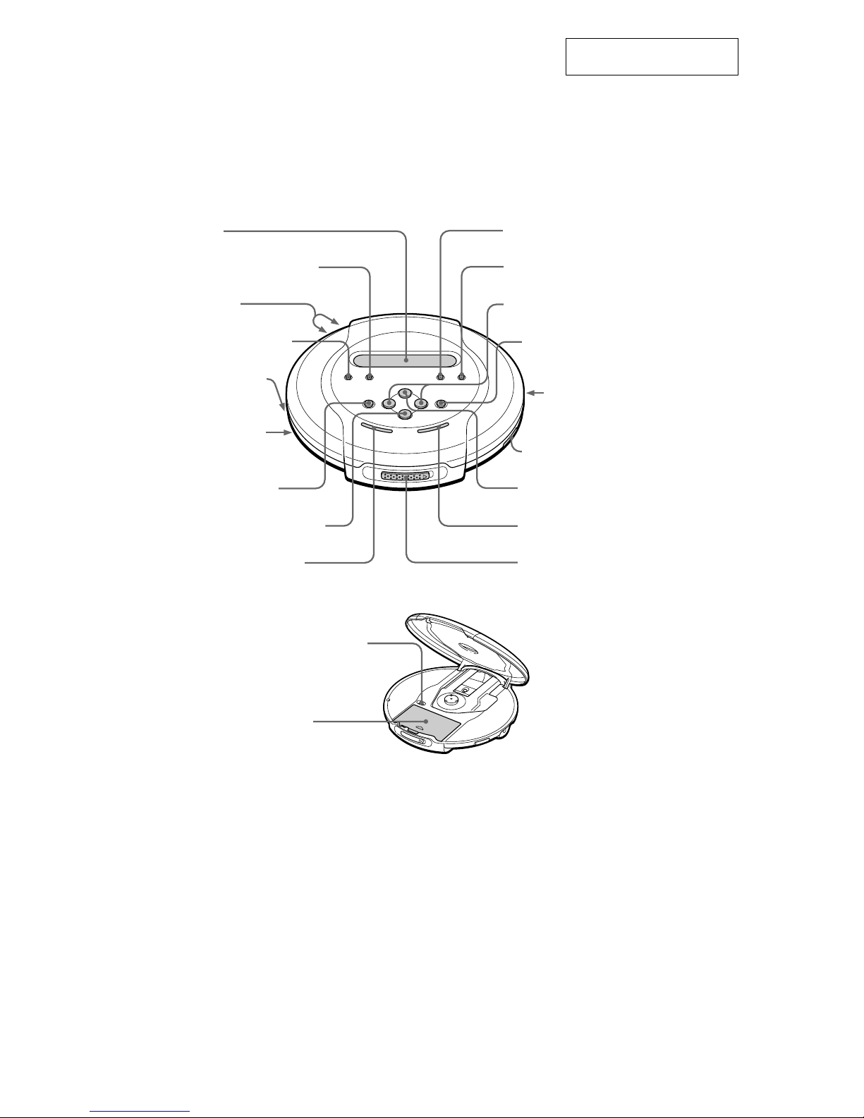
LOCA TING THE CONTR OLS
This section is extracted from
instruction manual.
CD player (front)
CD player (inside)
6 i (headphones)
qa DISPLAY button
w; Battery
compartment
1 Display
7 FOLDER – button
qg HOLD switch
qk OPEN switch
2 REPEAT / ENTER button
qf DC IN 4.5 V
(external power
input)jack
qh NX * (play / pause)button
8 x (stop) / CHARGE button
qs 'm / M' (AMS / search)
button
ql G-PROTECTION
switch
5 LINE OUT jack
qd FOLDER + button
9 VOL(volume) – button
qj VOL(volume) +*
4 PLAY MODE button
3 Strap holes
0 SOUND button
*The button has a tactile dot.
5
D-CJ01
SECTION 3
DISASSEMBLY
Note : Follow the disassembly procedure in the numerical order given.
3-1. CABINET (LOWER) SUB ASSY, CABINET ( INNER ) SUB ASSY
3-2. MD MECHANISM
z
The equipment can be removed using the following procedure.
4
Screws (B2)
Cabinet (inner) sub ASS
Y
5
Claws
2
Open
1
Screws (B2)
7
Cabinet (lower) sub ASSY
6
Claws
Open the battery case lid
3
Set
Cabinet (lower) sub ASSY
Cabinet (inner) sub ASSY
MD mechanism
Switch unit
Main board
"Motor ASSY (sled) (M902)", Optical pick-up (DAX-23E)
"Motor ASSY, Turn table (spindle) (M901)"
1
Optical pick-up flexibe board
2
CN502 (green)
3
CN503 (white)
Cabinet (lower) sub ASS
Y
MD MECHANISM
4
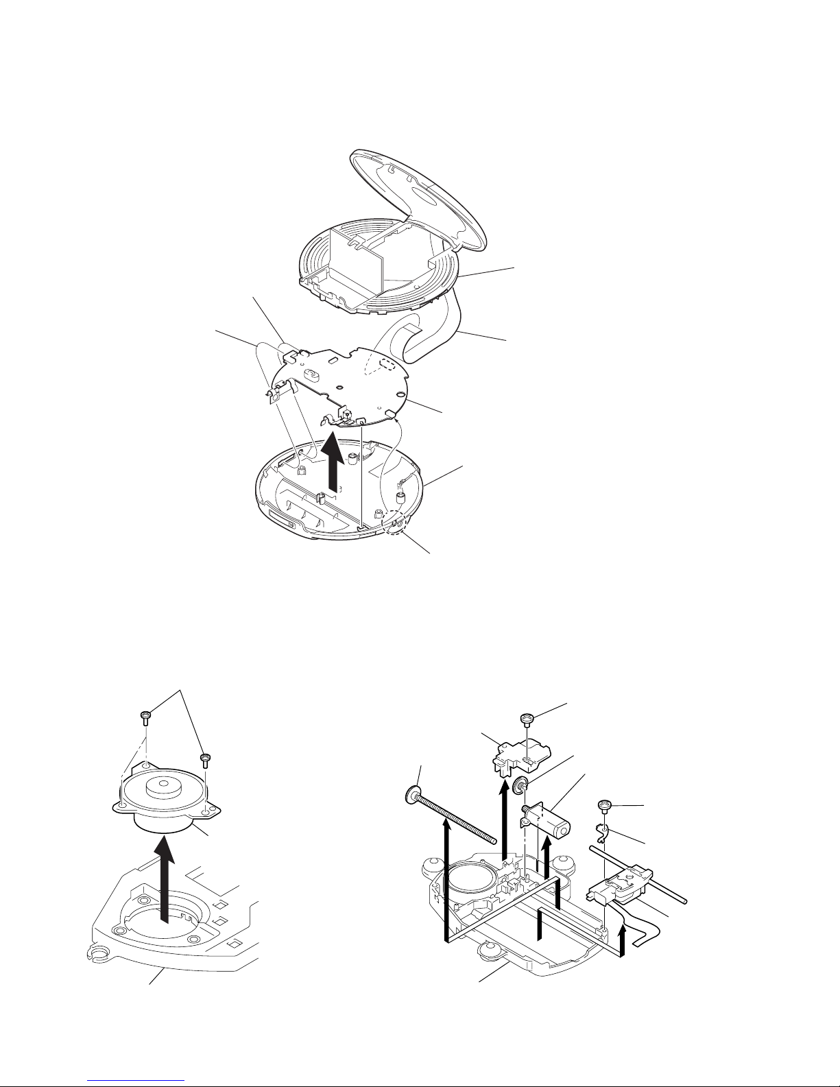
6
D-CJ01
3-4. “MO TOR ASSY, TURN T ABLE
(SPINDLE) (M901)”
3-5. “MOTOR ASSY (SLED) (M902)”,
OPTICAL PICK-UP (DAX-23E)
2
Motor ASSY, Turn tabl
e
(Spindle) (M901)
1 Screws
(B1.7x5)
Chassis
3-3. MAIN BOARD
2
J302
4
3
J301
5
Flexble board
1
J401
Cabinet (lower) sub ASSY
Cabinet (inner) sub ASS
Y
Main board
3
5
6
2
1 Screw (B 1.7x5)
4 Screw
(P 1.4x3.5)
Screw ASSY, Feed
Chassis
Optical pick-up
(DAX-23E)
Retainer, shaft
Gear B
Cover, Gear
Motor ASSY (Sled) (M902)
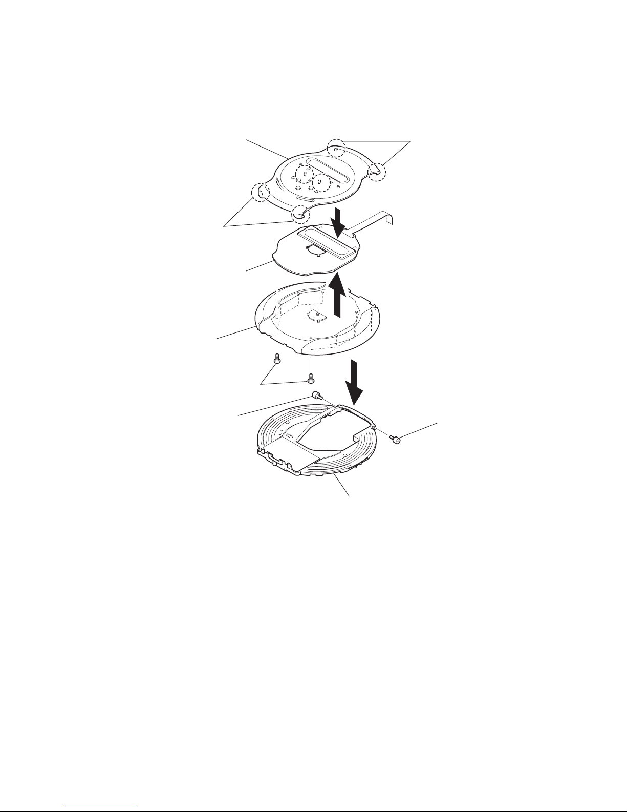
7
D-CJ01
3-6. SWITCH UNIT
5
Claws
3
Screws
5
Claws
Lid (B) upper ASSY
Switch unit
Cabinet (inner) sub ASSY
Lid (A) upper ASSY
6
4
2
1
Screws
1
Screw
s
8
D-CJ01
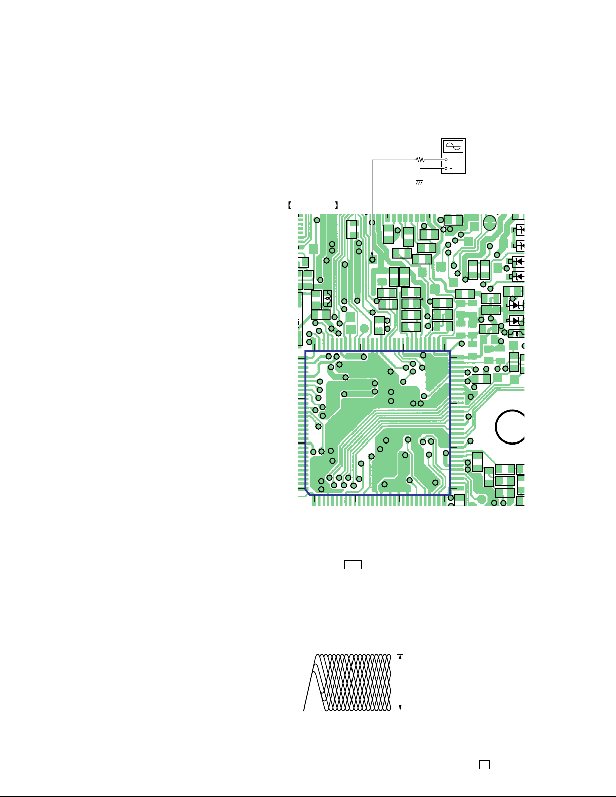
Procedure:
1. Connect the oscilloscope to the test points TP614 (RF) and TP635
(GND) on the MAIN board.
2. Set a disc. (YEDS-18)
3. Press the u button.
4. Check the oscilloscope waveform is as shown below.
A good eye pattern means that the diamond shape (◊) in the center of the waveform can be clearly distinguished.
RF Signal reference Waveform (Eye Pattern)
To watch the eye pattern, set the oscilloscope to AC range and
increase the vertical sensitivity of the oscilloscope for easy
watching.
5. Stop revolving of the disc motor by pressing the x button.
SECTION 4
ELECTRICAL ADJUSTMENTS
The CD section adjustments are done automatically in this set.
Precautions for Check
1. Perform check in the order given.
2. Use YEDS-18 disc (Part No.: 3-702-101-01) unless otherwise
indicated.
3. Power supply voltage requirement : DC4.5 V in DC IN jack.
(J401)
VOLUME button : Minimum
HOLD switch : OFF
Focus bias Check
Condition:
• Hold the set in horizontal state.
Connection:
RF level
0.4 to 0.8 Vp-p
VOLT/DIV : 100 mV (With the 10 : 1 probe in use
)
TIME/DIV : 500ns
110
90
TP608
TP609
AP605
C637
C636
C627
L602
91
TP626
30
R811
R810
R643
TP614
(RF)
TP506
TP507
SL409
C508
TP514
TP508
R503
C510
C507
TP613
C60
T
R505
R506
C309
C657
D101
C619
R634
R633
C618
R635
C625
C622
TP513
R504
C506
TP617
TP60
5
S
TP509
TP616
C610
R618
R629
R613
R614
61
60
70
R210 C
2
C106
R110
R109
R209
31
40
51
20
IC601
AP603
52
30
TP611
R662
R641
R630
C105
C
2
R609
R608
1
80
20
10
C501
9
16
MAIN BOARD (SIDE A)
TP614 (RF)
2K
Ω
oscilloscope
(AC range)
9
D-CJ01
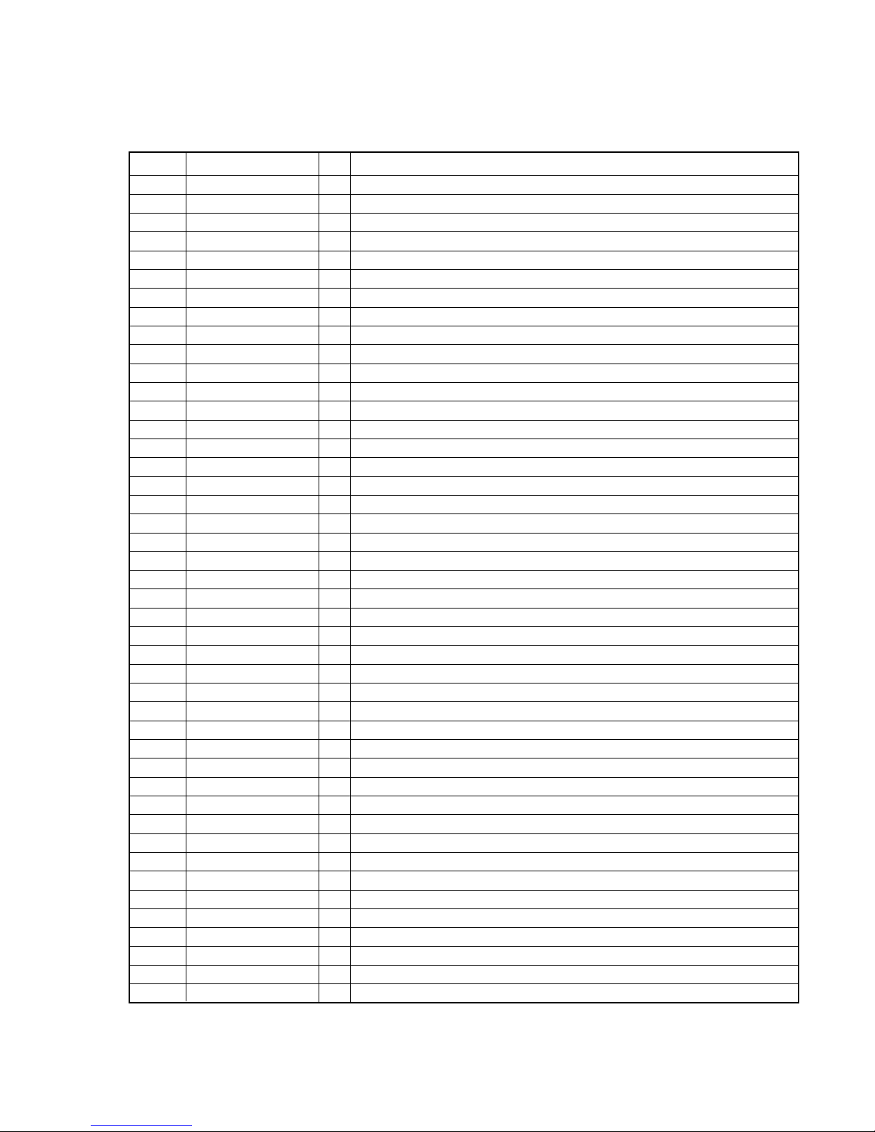
Pin No. Pin name I/O Description
1 CEX — Not used (OPEN).
2 to 8 — — Not used (OPEN).
9 VDD — Power supply terminal.
10 XTAL 0 O Crystal oscillator output (8MHz).
11 XTAL 1 I Crystal oscillator input (8MHz).
12 GND — Ground terminal.
13 — — Not used (OPEN).
14 GND — Ground terminal.
15 RESET I Reset terminal.
16 SCOR I Sob code signal input.
17 GRSCOR I GR SCOR signal input.
18 OPENSW I Open/Close switch input.
19 KEY I Main unit Key input.
20 RMKEY I Rrmote control Key input.
21 DCIN I AC adaptor detection.
22 — — Not used (OPEN).
23 VDD ( AVDD ) — Power supply terminal.
24 VDD ( AVREFO ) — Power supply terminal.
25 BATT 1 MNT I Battery input (3V).
26 BATT 2 MNT I Battery input (1.5V).
27 CHGMNT I Charge moniter input.
28 KEY 1 I Main unit Key input.
29 KEY 2 I Main unit Key input.
30 RMKEY I Rrmote control Rey input.
31 DCINMNT I Not used (OPEN).
32 — — Not used (OPEN).
33 GND ( AVSS ) — Ground terminal.
34 AGC O AGC output.
35 — — Not used (OPEN).
36 VDD ( AVREF 1 ) — Power supply terminal.
37 TSBDT 1 I TSB data input.
38 TSBDT 0 O TSB data output.
39 TSBSCK I TSB serial clock data input.
40 SENS I Sequencer input.
41 SDTO O Serial data output.
42 SCK O Serail data transfer clock signal output.
43 MCLK O Clocr signal output for RM control.
44 BEEP O Beep signal output.
45 SDAO O Serail data output for MPEG decorder.
46 XSOE O SOE signal output for IC601.
47 SCLO O Serail clock output.
48 XPOWLT O Power ON/OFF signal output.
49 XAPCOFF O Autmatic power control off signal output.
50 XHGON O HG on signal output.
SECTION 5
DIAGRAMS
5-1. EXPLANATION OF IC TERMINALS
IC801 (SYSTEM CONTROL) µPD784216AY-CJ1

10
D-CJ01
51 AMUTE O Audio mute signal output.
52 VCC 2 ON O HP amplifier ON/OFF output.
53 XRST I Reset terminal.
54 WAKE UP O Wakeup signal output.
55 XLAT O Latch signal output.
56 to 63 D 0 to D 7 O LCD drive output.
64 AO O LCD drive output.
65 to 71 — — Not used (OPEN).
72 GND — Ground terminal.
73 to 76 — — Not used (OPEN).
77 RD O RD output for switch unit.
78 WR 1 O WR 1 output for switch unit.
79 to 80 — — Not used (OPEN).
81 VDD — Power supply terminal.
82 XQOK O Q signal OK output for IC601.
83 TSB RW O TSB RW signal output for IC802.
84 TSBLAT O TSB lach output for IC802.
85 BUSY I BUSY signal input form IC601.
86 FOK I FOK signal input form IC601.
87 GFS I GFS signal input form IC601.
88 GPRO I G PROTECTION switch input.
89 XWRE O WRE signal output form IC601.
90 HOLD I HOLD switch input.
91 LINE IN I LINE IN jack detect input.
92 XRDE O RDE output for IC601.
93 TEST MODE I Test mode setting terminal.
94 GND — Ground terminal.
95 STANDBY O STANDBY output for IC606.
96 MP3 DSP RST O MP3 DSP reset output for IC606.
97 LCD RST O LCD reset output.
98 MP3 DSP I MP3 DSP status input.
99 to 100 — — Not used (OPEN).
 Loading...