

Sony VPD-MX10,RM-PJM11 Service Manual
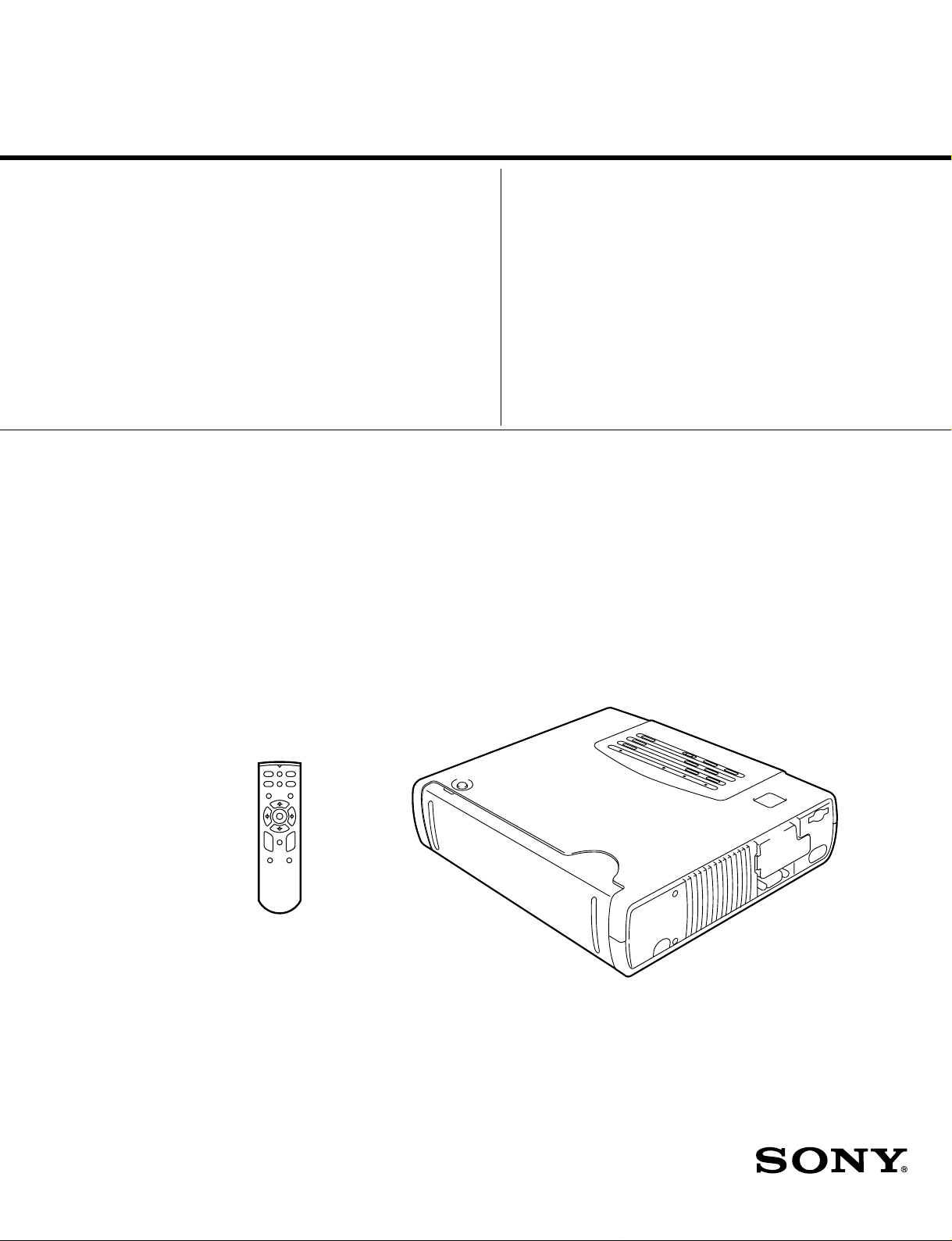
SERVICE MANUAL
MODEL
.............. .........
DEST. MODEL DEST.
.............. .........
VPD-MX10 WORLD RM-PJM11 WORLD
DATA PROJECTOR

! WARNING
This manual is intended for qualified service personnel only.
To reduce the risk of electric shock, fire or injury, do not perform any servicing other than that
contained in the operating instructions unless you are qualified to do so. Refer all servicing to
qualified service personnel.
! WARNUNG
Die Anleitung ist nur für qualifiziertes Fachpersonal bestimmt.
Alle Wartungsarbeiten dürfen nur von qualifiziertem Fachpersonal ausgeführt werden. Um die
Gefahr eines elektrischen Schlages, Feuergefahr und Verletzungen zu vermeiden, sind bei
Wartungsarbeiten strikt die Angaben in der Anleitung zu befolgen. Andere als die angegeben
Wartungsarbeiten dürfen nur von Personen ausgeführt werden, die eine spezielle Befähigung
dazu besitzen.
! A VERTISSEMENT
Ce manual est destiné uniquement aux personnes compétentes en charge de l’entretien. Afin
de réduire les risques de décharge électrique, d’incendie ou de blessure n’effectuer que les
réparations indiquées dans le mode d’emploi à moins d’être qualifié pour en effectuer d’autres.
Pour toute réparation faire appel à une personne compétente uniquement.
WARNING!!
AN INSULATED TRANSFORMER SHOULD BE USED DURING
ANY SERVICE TO AVOID POSSIBLE SHOCK HAZARD, BECAUSE OF LIVE CHASSIS.
THE CHASSIS OF THIS RECEIVER IS DIRECTL Y CONNECTED
TO THE AC POWER LINE.
SAFETY-RELATED COMPONENT WARNING !!
COMPONENTS IDENTIFIED BY A
DIAGRAMS, EXPLODED VIEWS AND IN THE P ARTS LIST ARE
CRITICAL TO SAFE OPERATION. REPLACE THESE COMPONENTS WITH SONY P ARTS WHOSE P ART NUMBERS APPEAR
AS SHOWN IN THIS MANUAL OR IN SUPPLEMENTS PUBLISHED BY SONY.
!!
! MARK ON THE SCHEMA TIC
!!
ATTENTION!!
AFIN D’ÉVITER TOUT RISQUE D’ÉLECTROCUTION
PROVENANT D’UN CHÂSSIS SOUS TENSION, UN
TRANSFORMATEUR D’ISOLEMENT DOIT ETRE UTILISÉ LORS
DE TOUT DÉPANNAGE.
LE CHÂSSIS DE CE RÉCEPTEUR EST DIRECTEMENT
RACCORDÉ Á L’ALIMENTATION SECTEUR.
ATTENTION AUX COMPOSANTS RELATIFS Á LA
LES COMPOSANTS IDENTIFIÉS PAR UNE MAPQUE
LES SCHÉMAS DE PRINCIPE, LES VUES EXPLOSÉES ET LES
LISTES DE PIECES SONT D’UNE IMPORTANCE CRITIQUE
POUR LA SÉCURITÉ DU FONCTIONNEMENT. NE LES
REMPLACER QUE PAR DES COMPOSANTS SONY DONT LE
NUMÉRO DE PIÈCE EST INDIQUÉ DANS LE PRÉSENT MANUEL
OU DANS DES SUPPLÉMENTS PUBLIÉS PAR SONY.
SÉCURITÉ!!
!!
! SUR
!!
For the customers in the Netherlands
Voor de klanten in Nederland
•Gooi de batterij niet weg, maar lever hem
in als KCA.
NL


Table of Contents
1. Service Informations
1-1. Board Layout...............................................................................................1-1
1-2. Disassembly and Extension Boards ............................................................1-2
1-2-1.Top Cover and H Board Removal ...................................................1-2
1-2-2.BB Board Removal..........................................................................1-3
1-2-3.B Block (BC and BA boards) Removal .......................................... 1-3
1-2-4.BC Board Removal..........................................................................1-4
1-2-5.BA Board Removal .........................................................................1-4
1-2-6.Power Block Removal ..................................................................... 1-5
1-2-7.QA Board Removal .........................................................................1-5
1-2-8.Lamp Power Block Removal...........................................................1-6
1-2-9.NF Board Removal..........................................................................1-6
1-2-10.Extension Boards and Extension Cables Connection....................1-7
1-3. Power Cord..................................................................................................1-8
2. Electrical Adjustments
2-1. Preparations.................................................................................................2-1
2-1-1. Equipment Required...................................................................2-1
2-1-2. Setting the FActory Mode ..........................................................2-1
2-2. Adjust Signal Level.....................................................................................2-1
2-2-1. Component Level Adjustment ................................................... 2-1
2-2-2. Adjust VIDEO NTSC Level ...................................................... 2-1
2-3. White Balance Adjustment ......................................................................... 2-2
2-3-1. White Balance Adjustment of INPUT-A ...................................2-2
2-3-2. White Balance Adjustment of VIDEO.......................................2-2
2-4. Memory .......................................................................................................2-3
2-5. Adjustment Item Initialize Data ..................................................................2-4
3. Semiconductors
IC.................................................................................................................3-1
Transistor.....................................................................................................3-3
Diode ...........................................................................................................3-4
VPD-MX10
1

4. Spare Parts
4-1. Notes on Repair Parts..................................................................................4-1
4-2. Exploded Views ..........................................................................................4-2
4-2-1. Cover ..........................................................................................4-2
4-2-2. Chassis 1.....................................................................................4-3
4-2-3. Chassis 2.....................................................................................4-4
4-2-4. Optical Unit ................................................................................4-5
4-3. Electrical Parts List .....................................................................................4-6
5. Block Diagrams
H Block .......................................................................................................5-1
QA Block .................................................................................................... 5-1
BC Block ..................................................................................................... 5-1
BA Block.....................................................................................................5-2
BB(1/2) Block .............................................................................................5-4
NF Block .....................................................................................................5-5
BB(1/2) Block .............................................................................................5-4
6. Diagrams
6-1. Frame Schematic Diagram .......................................................................... 6-1
6-2. Schematic Diagrams and Printed Wiring Boards........................................6-3
Schematic Diagrams
BA .........................................................................................................6-5
BB .......................................................................................................6-12
H .......................................................................................................6-22
BC .......................................................................................................6-23
QA .......................................................................................................6-24
NF .......................................................................................................6-24
Printed Wiring Boards
BA ......................................................................................................... 6-4
BB .......................................................................................................6-10
H .......................................................................................................6-22
BC .......................................................................................................6-22
QA .......................................................................................................6-24
NF .......................................................................................................6-24
2
VPD-MX10

1-1. Board Layout
Section 1
Service Informations
BB
NF
Lamp power
H
BA
Power block
BC
QA
VPD-MX10
1-1

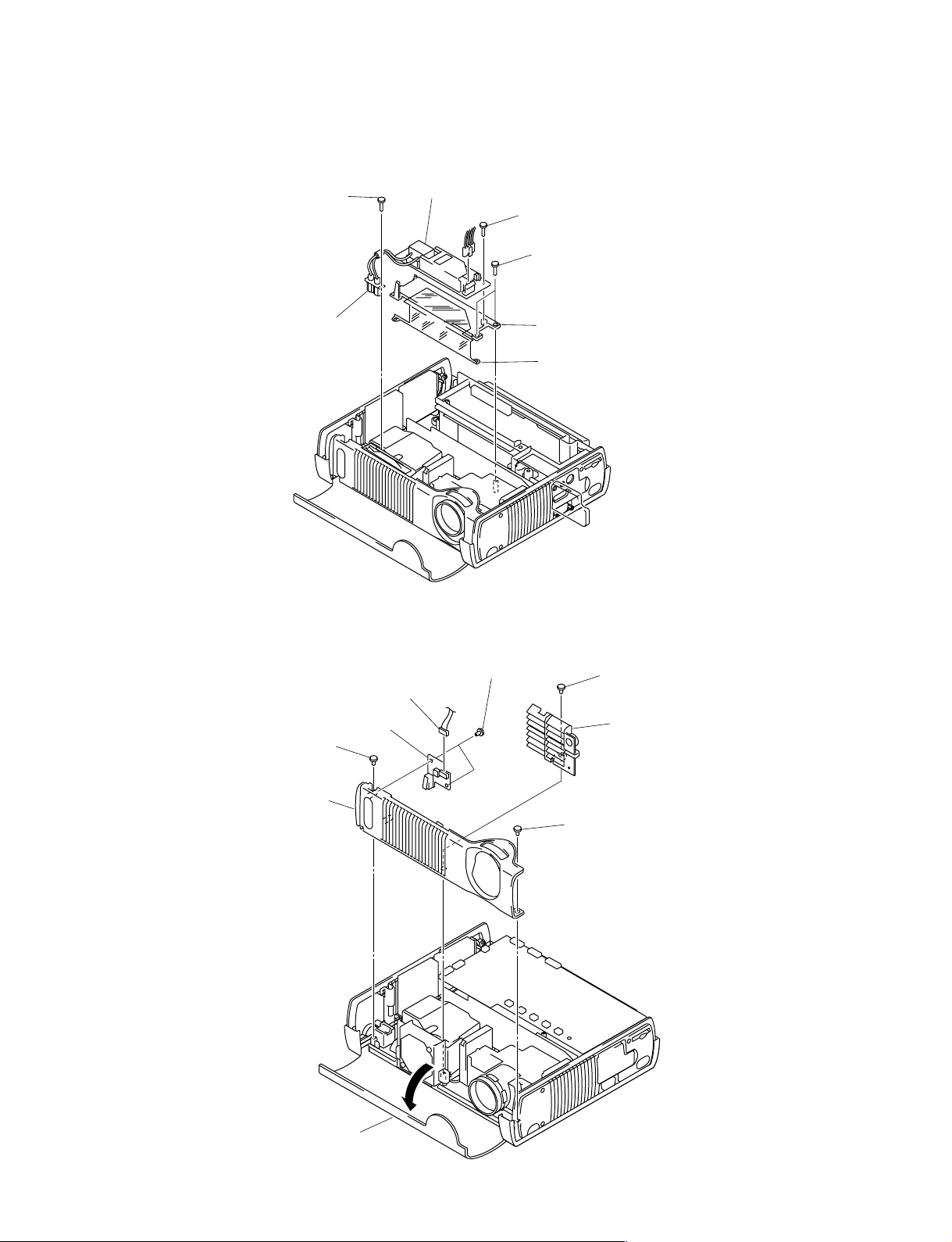
1-2. Disassembly and Extension Boards
1-2-1. Top Cover and H Board Removal
2 Top cover assy
6 Key power
3 Two screws (H)
7 Key control
CN1
5 H board
4 Four screws (H)
1-2
1 Shaft
VPD-MX10

1-2-2. BB Board Removal
CN1010
CN1005
CN1008
CN1001
CN1000
CN1004
CN1014
CN1003
CN1011
CN1012
1 Two screws
(+B2.6 x 4)
CN1013
2 BB board
1-2-3. B Block (BC and BA boards) Removal
3 Two screws
(+B2.6 x 4)
4 B block assy
2 Connector screws
1 Connector cover
VPD-MX10
1-3
1-2-4. BC Board Removal
* Remove the B Block. (Refer to Sec.1-2-3.)
2 BC board
B block assy
1 Screw
(+B2.6 x 4)
1-2-5. BA Board Removal
* Remove the B Block. (Refer to Sec.1-2-3.)
* Remove the BC Board. (Refer to Sec.1-2-4.)
B block holder
2 BA board
Sheet (B) assy
1-4
1 Two screws
(+B2.6 x 4)
VPD-MX10
1-2-6. Power Block Removal
* Remove the B Block. (Refer to Sec.1-2-3.)
3 Power block
4 Seet (G)
2 Two screws
(+B2.6 x 4)
1 AC holder
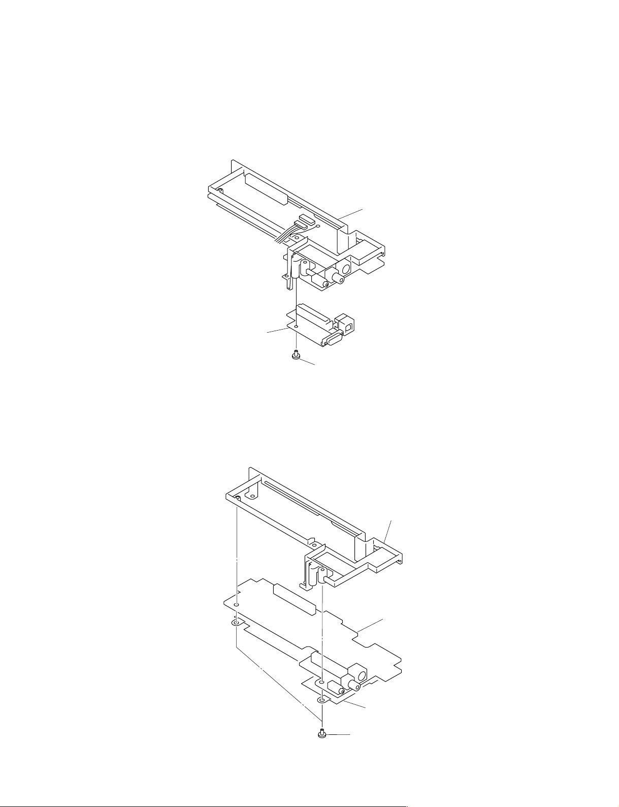
1-2-7. QA Board Removal
* Remove the B Block. (Refer to Sec.1-2-3.)
2 Screw
(+B2.6 x 4)
CN1101
3 QA board
1 T wo connector
screws
VPD-MX10
1-5
1-2-8. Lamp Power Block Removal
1 Screw
(+PTPWH2.6 x 4)
Lamp power connector (2P)
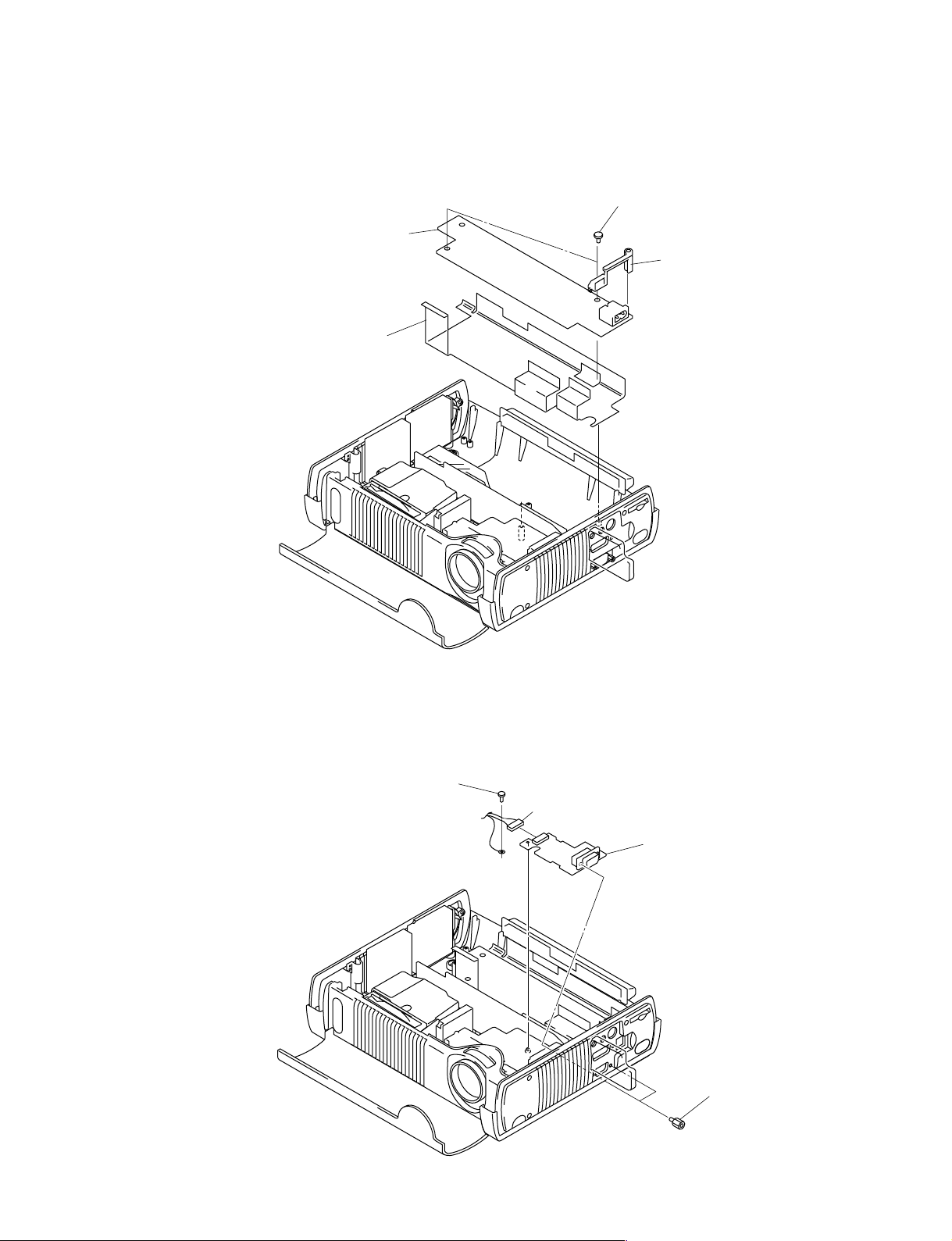
1-2-9. NF Board Removal
CN870
6 Lamp power
7 Two screrws
(+BVTP 3 x 6)
5 Screw
(+B2.6 x 4)
2 Two screws
(+B2.6 x 4)
3 Lamp power holder
4 Sheet (LPW)
4 Screw
(+B 2.6 x 4)
2 Screw
(+B 2.6 x 4)
6 Front panel
1 Front cover
8 NF board
5 Slit (F)
3 Screw
(+B 2.6 x 4)
1-6
VPD-MX10
1-2-10.Extension Boards and Extension Cables Connection
Flexible Cable
XB Board
XA Board
Extension Board
XB Board
XA Board : A-1400-240-A
XB Board : A-1400-239-A
Flexible Cable(50P) : 1-900-258-22
Cable
(5pin)
XA Board
Flexible Cable
CN1002
CN901
Cable (12P) x1
(1-900-260-82)
X4 Board
(A-1391-140-A)
Two Screws(+B2.6 x 4)
Cable (5P) x1
(1-900-260-80)
X5 Board
(A-1391-141-A)
BB Board
X5 Board
X4 Board
Cable
(12pin)
XB Board
XA Board
XB Board
Cable
XA-XB
(50pin)
XA Board
BA Board
VPD-MX10
1-7
1-3. Power Cord
Use a proper power cord for your local power supply.
The United Continental UK Australia Japan
States, Canada Europe
Plug type YP-11 YP-21 SP-61 B8 YP-13
Female end YC-13L YC-13L YC-13L C7-2 YC-13L
Cord type SPT-2 H03VVH2-F H03VVH2-F H03VVH2-F VCTFK
Rated Voltage & Current 10 A/125 V 2.5 A/250 V 2.5 A/250 V 2.5 A/250 V 7 A/125 V
Safety approval UL/CSA VDE BS SAA DENAN
1)Use the correct Plug for your country.
1-8
VPD-MX10
Section 2
Electrical Adjustments
2-1. Preparations
2-1-1. Equipment Requitred
. Oscilloscope
Tektronix 2465 or equivalent
(bandwidth: 350 MHz or more)
. NTSC, PAL, SECAM component signal generator
Tektronix TG2000 + AVG1 (optionalmodule)
+AWVG1 (optionalmodule) or equivalent
. VG (Programmable video signal generator)
VG814 or equivalent
. Digital voltmeter
Advantest TR6845 or equivalent
. Luminance meter
. Chrominance difference gauge
Note: Perform the following adjustments at least 5
minutes after turning on the power.
2-1-2. Setting the Factory Mode
1. Check that the STATUS is ON in MENU.
2. Exit MENU.
3. Press the keys in the following order;
“ENTER” → “ENTER” → “LEFT” → “ENTER”.
4. The message “Do you wish to enter into the FACTORY MODE?” will be displayed.
5. Select YES.
2-2. Adjust Signal Level
2-2-1. Component Level Adjustments
1. Input the Component signal to the INPUT-A. Then, from
INPUT-A of the SET SETTING, select the COMPONENT (15K Component color bar chroma ON).
2. Set the COLOR to 45.
3. Connect the Oscilloscope to the TP300 (B OUT) of the
BA board .
4. Enter the item OTHER of Device Adjust of the menu.
5. Set 06 3D GAMMA/ THROUGH : 0 to 06 3D GAMMA/ THROUGH : 1.
6. Set 07 3D GAMMA/ SW : 1 to 07 3D GAMMA/ SW : 0.
7. Advance the item RGB-MTRX of Device Adjust of
the menu.
8. Select the item 08 YUV COL. Use the key ← or →, or
both, to adjust level of two color bars, the left and right
end so that they will come to the same level.
9. Select 09 SUB HUE, then adjust the level of centrally
adjoining two color bars in the midst of all bars, using
the key ← or →, or both so that they can be made flat.
10. Press ENTER key and select “ SAVE TO MEMORY
“. For saving the data, press the ENTER again.
Adjust GND to bottom ege
in the DC 0.5 V range.
(15K Component color bar/Chroma ON)
Fig. 2-2-1
2-2-2. Adjust VIDEO NTSC Level
1. Input the NTSC 100% Color bar signal to the VIDEO
INPUT.
2. Connect the Oscilloscope to the TP300 of the BA
board.
3. Set the COLOR to 45.
4. Enter the item RGB MATRX of Device Adjust of the
menu.
5. Select the item 08 YUV COL. Use the key ← or →, or
both, to adjust the level of two color bars, the left and
right end so that they will come to the same level.
6. Select the item 09 SUB HUE, then adjust the level of
centrally adjoining two color bars in the midst of all
bars, using the key ← or →, or both so that they can be
made flat.
7. Press the ENTER key and select “ SAVE TO MEMORY “. For saving the data, press the ENTER key again.
8. Perform alike for PAL (PAL 100% Color bar signal)
system in the same manner.
NTSC 100% Color bar
PAL 100% Color bar
Fig. 2-2-2
VPD-MX10
2-1

2-3. White Balance Adjustment
2-3-1. White Balance Adjustment of INPUT-A
7. BIAS G and B in the HIGH Mode of W/B an adjusted
so that the chromaticity (x, y) may become the following standard value.
1) HIGH Mode of INPUT-A
1. Input the 80 IRE FLAT FIELD signal (XGA signal) to
INPUT-A.
2. GAIN R and B in the HIGH Mode of W/B an adjusted
so that the chromaticity (x, y) may become the following standard value.
Standard value (x, y) = (0.290 ± 0.002, 0.330 ± 0.004)
3. Set the INPUT signal to the 20 IRE.
4. BIAS R and B in the HIGH Mode of W/B an adjusted
so that the chromaticity (x, y) may become the following standard value.
Standard value (x, y) = (0.290 ± 0.002, 0.330 ± 0.004)
5. It carries out by repeating the above-mentioned steps 2
and 4 and memory of the adjustment value is carried
out.
2) LOW Mode of INPUT-A
1. The data in the HIGH Mode of 2) is copied.
2. Input the 80 IRE FLAT FIELD signal (XGA signal) to
INPUT-A.
3. The following value is written in GAIN R, G and B of
data value which HIGH Mode copied, and the memory
of the chromaticity (xlow, ylow) is carried out.
Write-in value GAIN R : +15step
GAIN G : _15step
GAIN B : ±0step
Standard value (x, y) = (xlow ± 0.002, ylow ± 0.004)
8. It carries out by repeating the above-mentioned steps 5
and 7 and memory of the adjustment value is carried
out.
2-3-2. White Balance Adjustment of VIDEO
1) HIGH Mode of VIDEO
1. Input the 15K component signal (80 IRE FLAT
FIELD) to INPUT-A.
2. W/B GAIN and BIAS value are made into the same
value as the adjustment of the above 2).
3. The memory only of the following value is written in
and carried out to the value of the above-mentioned
step 2.
Write-in value GAIN G : _15step
BIAS G : _5step
2) LOW Mode of VIDEO
1. Set the INPUT signal to the 25 IRE.
2. W/B GAIN and BIAS value are made into the same
value as the adjustment of the above 1).
3. The memory only of the following value is written in
and carried out to the value of the above-mentioned
step 2.
Write-in value GAIN G : _15step
BIAS G : _5step
4. Set the INPUT signal to the 20 IRE.
5. BIAS G and B in the HIGH Mode of W/B an adjusted
so that the chromaticity (x, y) may become the following standard value.
Standard value (x, y) = (xlow ±0.002, ylow ± 0.004)
6. Set the INPUT signal to the 80 IRE.
2-2
VPD-MX10

2-4. Memory
This model is composed of the following five Memory
blocks.
1. Set memory.
2. Status memory.
3. Channel memory.
4. Chroma memory.
5. W/B memory.
Gamma memory is realized in the gamma mode added by
OFF SET function of the Contrast / Brightness output
value to each device.
CPU Internal ROM : 256Kbyte Flash Memory
CPU Internal RAM : 16Kbyte
External NVM Memory : 16Kbyte EEPROM
Set Memory
Status
Memory
Channel
Memory
Chroma
Memory
W/B
Memory
Installation
Memory
No.01
No.02
No.03
INPUT-A Preset INPUT-B Preset
No.04
No.05
...
No.50
No.03
No.04
No.05
...
No.50
INPUT-MS Preset
No.53
No.54
No.55
...
No.60
Video
S Video
Input-A
Input-B
Input-MS
NT358/443/BW60
PAL/PAL-M/N/
SECAM/BW50
15k RGB
Component (15k)
Computer Others
HIGH
LOW
HIGH
LOW
Non Reverse upside down
Reverse upside down
CPU ROM External NVM CPU RAM
Set Memory
Status
Memory
Channel
Memory
Chroma
Memory
W/B
Memory
Installation
Memory
For your reference, data stream will be briefed as the
follows.
When plugged in first (Standby state), whole data in the
ROM are written in the NVM (Non volatile memory).
Turning Power ON, memory data required enough for
current video image are selected from each Memory block
and developed in the RAM where adjusting is performed.
Thus, data adjusted in the RAM are written and memorized
in the NVM, automatically when in the user mode, or
triggered by memory operation ( Item in Service / Special
Service ).
W / B and Device Adjust is adjusted by an user in the
Service mode or in the Special Service mode and memorized in NVM at performing memory operation. In this
moment any data adjusted in the factory will be lost.
Set Memory
No.01
No.02
INPUT-A
No.03
Preset
No.04
No.05
...
No.50
No.03
INPUT-B
No.04
Preset
No.05
...
No.50
Video
S Video
Input-A
Input-B
Input-MS
NT358/443/BW60
PAL/PAL-M/N/
SECAM/BW50
15k RGB
Component (15k)
Computer Others
HIGH
LOW
HIGH
LOW
Non Reverse upside down
Reverse upside down
Active memory copy
Status
Memory
Chroma Memory
W/B
Memory
Installation Memory
MemoryInitialize
INPUT-MS
Preset
INPUT-A
User
HIGH
LOW
No.53
No.54
No.55
...
No.60
No.71
...
No.90
No.91
...
No.110
VPD-MX10
2-3
2-5. Adjustment Item Initialize Data
MenuTitle ItemName
PICTURE CTRL CONTRAST 80 80 80 80 80
BRIGHT 50 50 50 50 50
COLOR 50 50 -50 HUE 50 50 -50 SHARP 50 50 -50 RGB ENHANCER - - 30 30 30
D.PICTURE OFF OFF OFF OFF GAMMA MODE - - GRAPHICS GRAPHICS GRAPHICS
COLOR TEMP LO W LOW HIGH HIGH HIGH
COLOR SYS AUTO AUTO - - VOLUE 50 50 50 50 50
INPUT SETTING
SET SETTING STATUS ON
INSTALL SETTING KEYSTONE MEM. OFF
INFORMATION fH
W/B ADJUST GAIN R
DOT PHASE
SIZE H
SHIFT
SCAN CONV
ASPECT
BLANKING
INPUT-A
AUTO INPUT SEL OFF
LANGUAGE ENGLISH
POWER SAVING OFF
DIGIT KEYSTONE 0
MENU POSITION CENTER
MENU COLOR STANDARD
LAMP TIMER
fV
ROM Ver
OPERA TION TIMER
PREVIOUS LAMP TIMER
G
B
BIAS R
G
B
SET
MEMORY
COMPUTER
INDICATION ONLY
INDICATION ONLY
INDICATION ONLY
INDICATION ONLY
INDICATION ONLY
INDICATION ONLY
CH MEMORY
VIDEO 1 S Video 1 INPUT-A INPUT-B MS
* : “DOT PHASE, SIZE H, SHIFT H/V, SCAN CONV, ASPECT and BLANKING” in the “INPUT SETTING” menu
have an initial value respectively in accordance with the input signal (PRESET MEMORY No.).
Note : There are nonadjustable items in accordance with the input signal.
2-4
VPD-MX10

STATUS
MEMORY
15 (*)
*
*
ON (*)
4:3 (*)
0 (*)
VIDEO-
HIGH
MemoryName
W/B MEMORY
VIDEO-LOW RGB-HIGH RGB-LOW
Remarks
VPD-MX10
170 175 170 175
170 165 170 165
170 160 170 160
80 80 180 80
80 80 140 80
80 80 140 80
2-5

DeviceName ItemName MemoryName Remarks
SET MEMORY CHROMA MEMORY
NT3.58/NT4,43
/BW60
PAL/PAL-M/N/
SECAM/BW50
15kRGB
Component
(15k)
Two times speed
Component
HDTV(YPbPr)
HDTV(GBR)
Include
two times speed
RGB MTRX/
D.COM/
CHROMA/ SHP GAIN
P.DRV/
SH/ SH1 4
PE/
CONTRAST
R DRIVE
G DRIVE
B DRIVE
SUB BRT 52
YUV CON 8 8 11 11 11 11 11
YUV COL 8 8 12 12 12 12 12
SUB HUE 5 8 7 7 7 7 7
CTI LVL 2 2 1 1 1 1 1
R-Y/R 11 11 13 10 13 13 13
R-Y/B 14 14 15 14 15 15 15
G-Y/R 7 6 8 5 8 8 8
G-Y/B 5 5 4 4 4 4 4
SUB SHP 1 1 1 1 1 1 1
SHPF0 1 1 1 1 1 1 1
PRE OVER 0 0 0 0 0 0 0
DMIC PIC 3
LTI LVL
VENH
SHP EQ
SHP F0 2 2 2 2 2 2 2
Y-OUT LVL
C-OUT LVL
Y-DL 5
S B-Y ADJ
S R-Y ADJ
S-INHBT
S-ID
S GP
S V-ID
BELL F0 0
HPF 0
INV CONT 0
SID LVL 206
PRG LVL 86
INSTALLATION
SC FILTER 3
BD ENABLE 1
WHITE PEAKING 10
DMD BIN
12
9 9 9 9 9 9 9 Fix ed V alue
999 9999
999 9999
111 1
5
11 11 11 11 11 11 11
000 0000
15
9
7
7
0
0
0
0
0
0
00 0
Fixed Value
Fixed Value
Fixed Value
Fixed Value
Fixed Value
Fixed Value
Fixed Value
Fixed Value
Fixed Value
Fixed Value
Fixed Value
Fixed Value
Fixed Value
Fixed Value
Fixed Value
Fixed Value
Fixed Value
Fixed Value
Fixed Value
Fixed Value
Fixed Value
Fixed Value
Fixed Value
Fixed Value
Fixed Value
Fixed Value
Fixed Value
Fixed Value
Fixed Value
Fixed Value
Fixed Value
Fixed Value
Fixed Value
Fixed Value
Fixed Value
Note : There are nonadjustable items in accordance with the input signal.
2-6
VPD-MX10
DeviceName ItemName MemoryName Remarks
SET MEMORY CHROMA MEMORY
NT358/NT443
/BW60
PAL/PAL-M/N/
SECAM/BW50
15kRGB
Component
(15k)
Two times speed
Component
HDTV(YPbPr)
HDTV(GBR)
Include
two times speed
3D GAMMA/ SUB CONT 0
SUB BRT 0
R OSD LVL 31
G OSD LVL 31
B OSD LVL 31
THROUGH 0
SW 1
APC THRES 25
APC LIMIT 32
OTHER/ H START 144
V START 22
H POSITION 34
TEMP LAMP
TEMP PANEL
LAMP FAN 1
PANEL FAN 1
LAMP FAN 2
PANEL FAN 2
SYNCHRONOUS 0
GAMMA
Adjustment is
impossible
Adjustment is
impossible
Adjustment is
impossible
Adjustment is
impossible
Adjustment is
impossible
Adjustment is
impossible
Factory default
setting value
Fixed Value
Fixed Value
Fixed Value
Fixed Value
Fixed Value
Fixed Value
Fixed Value
Fixed Value
Fixed Value
Fixed Value
Fixed Value
Fixed Value
Fixed Value
Fixed Value
Fixed Value
Fixed Value
Fixed Value
Fixed Value
Fixed Value
Note : There are nonadjustable items in accordance with the input signal.
VPD-MX10
2-7

Section 3
1
TOP VIEW
Semiconductors
IC
24LC21AT/SN
BA10393F-E2
IRMF-A0T-QTP
M24C64
M24C64-WMN6T(A)
MM1096AFF
NJM4558eM(TE2)
TC7W14FU(TE12R)
TC7W04FU
TC7W08FU
TC7W32FU
TC7WH04FU(TE12R)
TC7WH123fu(TE12R)
TC7WH74FK(TE85R)
TC7WH74FU(TE12R)
ST24FC21M6TR
1
TOP VIEW
8PIN SOP
CXA1875AM
CXA1875AM-T4
TC74HC148AF(EL)
LM4860MX
MM1231XFBE
1
TOP VIEW
16PIN SOP
74VHC02MTCX
74VHC125MTCX
BA10339FV
BA10339FV-E2
TC74LCX125FT
TC74LCX125FT(EL)
74LC541MTCX
74VHC240MTCX
74VHC541MTCX
74VHCT541AFT(EL)
CXA1846BN-T4
MK1714-01
MK1714-01RT
M52347FP-TE
1
TOP VIEW
20PIN SOP
AD9884AKS-140
65102
103
128
1
TOP VIEW
38
BA033F-E2
BA033FP-E2
BA05FP-E2
BA09F-E2
1
2
3
CXA2101AQ
CXA2101AQ-TL
CXA2123AQ
CXA2123AQ-T6
39
48
TOP VIEW
CXD2064Q(T6)
ISPLSI2032VE-110LT4
/10921
ISPLSI2032VE-110LT44
/1727PW
MB86189
MB86189PFV-G-BND-ER
64
39
1
TOP VIEW
48PIN QFP
CXD9607GB
A
1
BOTTOM VIEW
144PIN PGA
HD64F2633
HD64F2633TE
HM62V16256CLT5SLZ
MBM29LV400TC-70PFTN
SST39VF800A-70
SST39VF800A-70-1727A-T
2538
24
15
141
1
TOP VIEW
44PIN SOP
ISPLSI2064VE-100LT44
/1727A
UPD72012GB-003-3B4
1
TOP VIEW
44PIN QFP
LP2985IM5X3.3
LMC7101BIM5X
TC75S56F(TE85R)
TC7S04FU(TE85R)
TC7S08FU
TC7S08FU(TE85R)
TC7S14FU(TE85R)
TC7SET08FU(TE85R)
TC7SZ05(TE85L)
TC7SZ126(TE85L)
M52758FP
48PIN
MD2305F
A
1
BOTTOM VIEW
280PIN PGA
MT48LC8M16A2TG75
MT48LC8M16A2TG-75TR
1
TOP VIEW
54PIN TSOP
1
TOP VIEW
14PIN SOP
VPD-MX10
4164
61
80
1
TOP VIEW
40
91
25
24
120
1
TOP VIEW
6190
60
31
30
1
TOP VIEW
36PIN SOP
3-1
IC
PQ2TZ15U
1
PW365-10U
192 129
193
256
164
TOP VIEW
S-80828ANNP
S-80828ANNP-EDR-T2
S-80842ANNP
S-80842ANNP-ED6
S-80842ANNP-ED6-T2
1
5
TOP VIEW
4PIN CHIP
TA78M09F(TE16L)
128
65
1
2
3
RCV4-A1T-MASK-25
ST72T631K4M41-201
1
TOP VIEW
34PIN SOP
RS-140-T
4
1
2
THC63DV151
1
TOP VIEW
100PIN QFP
3
3-2
VPD-MX10
 Loading...