

Page 1

UNIVERSAL CONTROL PANEL
UCP-8060
MAINTENANCE MANUAL
1st Edition
Serial No. 10001 and Higher
Page 2

! WARNING
This manual is intended for qualified service personnel only.
To reduce the risk of electric shock, fire or injury, do not perform any servicing other than that
contained in the operating instructions unless you are qualified to do so. Refer all servicing to
qualified service personnel.
! WARNUNG
Die Anleitung ist nur für qualifiziertes Fachpersonal bestimmt.
Alle Wartungsarbeiten dürfen nur von qualifiziertem Fachpersonal ausgeführt werden. Um die
Gefahr eines elektrischen Schlages, Feuergefahr und Verletzungen zu vermeiden, sind bei
Wartungsarbeiten strikt die Angaben in der Anleitung zu befolgen. Andere als die angegeben
Wartungsarbeiten dürfen nur von Personen ausgeführt werden, die eine spezielle Befähigung
dazu besitzen.
! A VERTISSEMENT
Ce manual est destiné uniquement aux personnes compétentes en charge de l’entretien. Afin
de réduire les risques de décharge électrique, d’incendie ou de blessure n’effectuer que les
réparations indiquées dans le mode d’emploi à moins d’être qualifié pour en effectuer d’autres.
Pour toute réparation faire appel à une personne compétente uniquement.
UCP-8060
Page 3

For the U.S.A
Attention-when the product is installed in Rack:
1. Prevention against overloading of branch circuit
When this product is installed in a rack and is
supplied power from an outlet on the rack, please
make sure that the rack does not overload the supply
circuit.
WARNING
This unit has no power switch.
When installing the unit, incorporate a readily
accessible disconnect device in the fixed wiring, or
connect the power cord to a socket-outlet which must
be provided near the unit and easily accessible, so that
the user can turn off the power in case a fault should
occur.
2. Providing protective earth
When this product is installed in a rack and is
supplied power from an outlet on the rack, please
confirm that the outlet is provided with a suitable
protective earth connection.
3. Internal air ambient temperature of the rack
When this product is installed in a rack, please make
sure that the internal air ambient temperature of the
rack is within the specified limit of this product.
4. Prevention against achieving hazardous
condition due to uneven mechanical loading
When this product is installed in a rack, please make
sure that the rack does not achieve hazardous
condition due to uneven mechanical loading.
5. Install the equipment while taking the operating
temperature of the equipment into consideration
For the operating temperature of the equipment, refer
to the specifications of the Operation Manual.
6. When performing the installation, keep the rear of
the unit 10 cm (4 inches) or more away from walls
in order to obtain proper exhaust and radiation of
heat.
WARNUNG
Dieses Gerät hat keinen Netzschalter.
Beim Einbau des Geräts ist daher im Festkabel ein
leicht zugänglicher Unterbrecher einzufügen, oder das
ß
Netzkabel mu
mit einer in der Nähe des Geräts
befindlichen, leicht zugänglichen Wandsteckdose
verbunden werden, damit sich bei einer
Funktionsstörung die Stromversorgung zum Gerät
jederzeit unterbrechen läßt.
When using a LAN cable:
For safety,do not connect to the connector for
peripheral device wiring that might have excessive
voltage.
UCP-8060
1 (P)
Page 4

Page 5

Table of Contents
Manual Structure
Purpose of this manual ........................................................................................ 3 (E)
Related manuals................................................................................................... 3 (E)
Contents ............................................................................................................... 4 (E)
Trademarks .......................................................................................................... 4 (E)
1. Service Overview
1-1. Removing the Upper Panel ...................................................................1-1 (E)
1-2. Main Parts Location ..............................................................................1-1 (E)
1-3. System Indicator and Status Indicator...................................................1-2 (E)
1-3-1. System Indicator...................................................................1-2 (E)
1-3-2. Status Indicator.....................................................................1-2 (E)
1-4. Troubleshooting ....................................................................................1-3 (E)
1-5. Replacing the Board ..............................................................................1-8 (E)
1-5-1. MB-978 Board .....................................................................1-8 (E)
1-5-2. CPU-352 Board ....................................................................1-9 (E)
1-5-3. TouchEngine Board .............................................................1-9 (E)
1-6. Replacing the Main Parts ....................................................................1-10 (E)
1-6-1. Switching Regulator ...........................................................1-10 (E)
1-6-2. Rotary Encoder...................................................................1-11 (E)
1-6-3. Inverter Unit .......................................................................1-12 (E)
1-6-4. LCD Panel ..........................................................................1-13 (E)
1-6-5. Back Light ..........................................................................1-14 (E)
1-6-6. Touch Panel........................................................................1-14 (E)
1-7. Replacing the Fuse/IC Link ................................................................1-15 (E)
1-8. Initializing System Setting Value........................................................1-15 (E)
1-9. System File Recovery .........................................................................1-16 (E)
UCP-8060
2. Spare Parts
2-1. Notes on Repair Parts.................................................................................. 2-1
2-2. Exploded Views .......................................................................................... 2-2
2-3. Electrical Parts List ..................................................................................... 2-5
2-4. Supplied Accessories List .........................................................................2-10
2-5. Power Cords List....................................................................................... 2-10
2-6. Optional Fixtures List ...............................................................................2-10
1 (E)
Page 6

3. Semiconductor Pin Assignments
4. Circuit Description and Overall Block Diagram
4-1. Circuit Description ................................................................................4-1 (E)
4-2. Overall Block Diagram ............................................................................... 4-2
5. Schematic Diagrams
CN-2284....................................................................................................5-1
CPU-352 ...................................................................................................5-2
KY-537 ....................................................................................................5-5
LED-397 ...................................................................................................5-6
MB-978 ....................................................................................................5-7
PS-635 ..................................................................................................5-12
SW-1098 ................................................................................................. 5-13
SW-1099 ................................................................................................. 5-13
VR-282 .................................................................................................. 5-14
Frame Wiring ..........................................................................................5-15
6. Board Layouts
CN-2284....................................................................................................6-1
CPU-352 ...................................................................................................6-1
KY-537 ....................................................................................................6-2
LED-397 ...................................................................................................6-2
SW-1099 ................................................................................................... 6-2
VR-282 .................................................................................................... 6-2
MB-978 ....................................................................................................6-3
PS-635 ....................................................................................................6-4
2 (E)
UCP-8060
Page 7

Purpose of this manual
Related manuals
Manual Structure
This manual is the maintenance manual of Universal Control Panel UCP-8060.
This manual is intended for use by trained system and service engineers, and
describes the information for maintenance and detailed service.
The following manuals are prepared for UCP-8060.
..
. Operation Manual (Supplied with UCP-8060)
..
This manual describes the notes on operating, the locations and functions of parts,
and controls of UCP-8060.
..
. Installation Manual (Supplied with UCP-8060)
..
This manual describes the information on installing the UCP-8060.
..
. User’s Guide (Available on request)
..
This manual describes the operations of the operation software.
If this manual is required, please contact your local Sony Sales Office/Service
Center.
..
. “Semiconductor Pin Assignments” CD-ROM (Available on request)
..
This “Semiconductor Pin Assignments” CD-ROM allows you to search for
semiconductors used in B&P Company equipment.
Semiconductors that cannot be searched for on this CD-ROM are listed in the
service manual for the corresponding unit. The service manual contains a complete list of all semiconductors and their ID Nos., and thus should be used together
with the CD-ROM.
Part number: 9-968-546-XX
UCP-8060
3 (E)
Page 8

Contents
This manual is organized by following sections.
Section 1 Service Overview
This section explains the information and procedure required for service such as
functions and operations of system indicator and status indicator, causes and
remedies of the troubles, and replacement of main parts.
Section 2 Spare Parts
This section describes the spare parts.
Section 3 Semiconductor Pin Assignments
This section contains information on semiconductors used for unit.
It includes a complete list of the semiconductors and their ID Nos. for retrieving
information on “Semiconductor Pin Assignments” CD-ROM, which is available
separately.
Please refer to this section together with the “Semiconductor Pin Assignments” CDROM.
Information on the semiconductors not contained in the CD-ROM at the time of
issue of this manual, if any, is given in this section as well.
Section 4 Circuit Description and Overall Block Diagram
This section describes the circuit description and overall block diagram.
Trademarks
Section 5 Schematic Diagrams
This section describes the schematic diagrams of each board, and frame wiring.
Section 6 Board Layouts
This section describes the board layouts and locatious of components.
Trademarks and registered trademarks used in this manual are follows.
. Java is a registered trademark of Sun Microsystems, Inc..
. Memory Stick is a trademark of Sony Corporation.
. MultiMediaCard is a trademark of Infineon Technologies AG.
. TouchEngine is a trademark of Sony Corporation.
Other system names, product names, and company names appearing in this manual
are trademarks or registered trademarks of their respective holders.
4 (E)
UCP-8060
Page 9
Section 1
LED-397 board
CPU-352 board
VR-282 board
CN-2284 board
TouchEngine board
TouchEngine board
SW-1098 board
PS-635 board
SW-1099
board
KY-537 board
MB-978 board
Touch panel
Switching regulator
LCD panel
Back light
Inverter unit
Back light
Service Overview
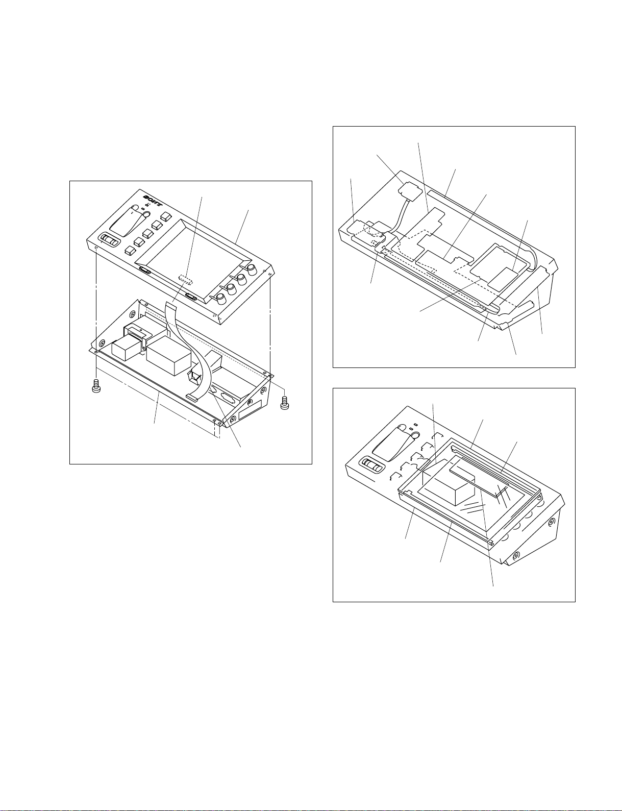
1-1. Removing the Upper Panel
1. Remove the six screws, then remove the upper panel.
2. Disconnect one flexible flat cable from the connector
(CN101) on the MB-978 board.
CN101
Upper panel
B 3x5
B 3x5
Lower panel
1-2. Main Parts Location
Flexible flat cable
UCP-8060
1-1 (E)
Page 10

1-3. System Indicator and Status Indicator
1-3. System Indicator and Status Indicator
1-3-1. System Indicator
The system indicator mainly indicates the operation status of the hardware.
The system indicator lights in red when the power is turned on. Generally it changes to amber soon, and
then to green when the system normally starts. If not, the indicator blinks in green or amber. In this case,
the system file needs to be reinstalled using the boot-up MMC (MultiMediaCard). (Refer to Section 1-9.)
Color of light Functions of indicator System operation/status
Red (lights) Lights on immediately after startup. Resetting hardware, etc.
Amber (lights) Indicates that the CPU started. Downloading Configuration data to FPGA
Green (lights) Indicates that the operation software started. Startup screen is displayed.
Green (blinks) Indicates that although the download of
Amber (blinks) Indicates that the download of Configuration data is
The indicator stays lit in red if there is no boot
program such as the case that nothing is written
in the flash memory.
The indicator changes to green when the (approx. 7 seconds)
download of Configuration data to FPGA is
completed. In case that the indicator stays lit in
amber, it means that a configuration error
(Configuration file is not normal, etc.) has occurred.
Configuration data is completed, an error was
detected in the initial check of FPGA.
failed and the UCP-8060 cannot start due to an error.
1-3-2. Status Indicator
The functions of status indicator at the power-on/restart are different from those when the Memory Stick
is used.
At the power-on/restart
The UCP-8060 checks the file of operation software installed and indicates the results with the status indicator.
..
. Amber (blinks)
..
Indicates that the status error related to the software is detected.
The status indicator blinks in amber when the UCP-8060 cannot start in such case that the system file is
damaged although the CPU is not damaged. At the same time, the system indicator lights in red or amber,
or blinks in amber.
The number of blinking varies depending on the type of error. In any case, install the system file again.
(Refer to the operation manual.)
n
The system file is checked before FPGA starts. Therefore the indication at the power-on /restart is not
mixed up with the status indication when the Memory Stick is used.
..
. Amber (Continuously blinks)
..
Indicates that FPGA is not normal. The system indicator blinks in amber at the same time.
If FPGA is not normal, the LCD module cannot be controlled. Therefore the system cannot start. In this
case, the system automatically tries to start the BIOS UTILITY after continuously blinking in amber for
ten times. If the BIOS UTILITY can be started, the communication via RS-232C is enabled.
1-2 (E)
UCP-8060
Page 11

When Memory Stick is used
Green (lights): Indicates that the data is read to the Memory Stick
Red (lights): Indicates that the data is written in the Memory Stick
Amber (lights): Indicates that the system is in other operation
1-4. Troubleshooting
Index
. Power cannot be turned on.
. Back light does not light.
. Buzzer does not sound.
. Function switch cannot be operated, or does not light.
. Control knobs cannot be operated.
. Jog roller or jog L or R button cannot be operated.
. Select L or R button cannot be operated.
. Data in the Memory Stick cannot be read.
. Although the back light is lit, nothing is displayed on the LCD panel.
. The UCP-8060 cannot communicate via RS-232C.
. The UCP-8060 cannot communicate via LAN.
. Touch panel does not operate.
. TouchEngine does not operate.
. TouchEngine is weak. (Sensitivity of the touch panel feels weak.)
. Clock does not operate.
. Back light is dark.
1-3. System Indicator and Status Indicator
1-4. Troubleshooting
Power cannot be turned on.
Status and possible cause Remedy
Power cord is disconnected. Check if the power cord is connected.
The UCP-8060 is starting up. Wait for a while.
(System indicator lights in amber) The system indicator changes to green in about 15 seconds
and the UCP-8060 starts up when it is in normal operation.
Fuse is blown. Replace the fuse (F101).
Power supply of 5 V, 3.3 V and 2.5 V are not Check if each power supply is normally output.
normally output. . 5 V : TP102, TP101/PS-635 board
System indicator lights in red. Replace the CPU (IC202) on the CPU-352 board. If the
. 3.3 V : TP102/MB-978 board
. 2.5 V : TP103/MB-978 board
5 V is not output.
Replace the AC/DC converter (CP101) on the PS-635 board.
If 5 V is not still output, replace the AC inlet (CN105).
5 V is output, but 3.3 V and 2.5 V are not output.
Check the connection of the harness between the PS-635
board and the MB-978 board.
If the power supply is not output although the connection is
correct, replace the corresponding regulator IC (IC101 or
IC102).
system indicator still lights in red, replace the flash ROM
(IC203).
UCP-8060
1-3 (E)
Page 12

1-4. Troubleshooting
Back light does not light.
Status and possible cause Remedy
Power is not turned on. Check if the power cord is connected.
Back light is broken. If the system indicator lights in green, replace the back light. If
the back light does not light after replacing the back light,
replace the inverter unit.
System indicator lights in red or amber. Replace the CPU (IC202) on the CPU-352 board.
Buzzer does not sound.
Status and possible cause Remedy
Sound Level is set to 0 in the Device Control Set the Sound Level to the level other than 0.
menu of the SYSTEM SETUP UTILITY.
(Refer to the operation manual.)
Buzzer is broken. If the buzzer does not sound although the Sound Level is set
to the level other than 0, replace the buzzer (BZ101).
Function switch cannot be operated, or does not light.
Status and possible cause Remedy
The connection between the KY-537 board and Check the operation in the Self Diagnosis menu of the
the MB-978 board is not correct. SYSTEM SETUP UTILITY. If the results of the Self Diagnosis
Function switch is broken.
It results from the specifications or setting of Check that the function switch lights in green → red → amber
operation software. (It is not failure.) sequentially every time it is pressed in the Self Diagnosis
are not normal, check the connection of the harness between
the KY-537 board and the MB-978 board. If the connection is
correct, replacethe corresponding function switch (S301S305/KY-537 board).
menu of the SYSTEM SETUP UTILITY. If the switch lights
sequentially, refer to the user’s guide of each operation
software and check the setting.
Control knob cannot be operated.
Status and possible cause Remedy
The connection between the VR-282 board and Check the operation in the Self Diagnosis menu of the
the MB-978 board is not correct. SYSTEM SETUP UTILITY. If the results of the Self
Rotary encoder is broken.
It results from the specifications or setting of Check the operation in the Self Diagnosis menu of the
operation software. (It is not failure.) SYSTEM SETUP UTILITY. If the control knob operates, refer
Diagnosis are not normal, check the connection of the
harness between the VR-282 board and the MB-978 board.
If the connection is correct, replace the corresponding rotary
encoder (EN201-EN204).
to the user’s guide of each operation software and check the
setting.
1-4 (E)
UCP-8060
Page 13

Jog roller, jog L button, or jog R button cannot be operated.
Status and possible cause Remedy
The connection between the SW-1099 board and Check the operation in the Self Diagnosis menu of the
the SW-1098 board is not correct. SYSTEM SETUP UTILITY. If the results of the Self Diagnosis
Jog roller is broken.
Jog L button or Jog R button is broken.
It results from the specifications or setting of Check the operation of the jog roller and jog L and R buttons
operation software. (It is not failure.) in the Self Diagnosis menu of the SYSTEM SETUP UTILITY.
are not normal, check the following.
Check the connection of the harness between the SW-
1098 board and the SW-1099 board.
If the connection is correct, the system indicator is lit and the
jog L and R buttons operate normally, replace the jog roller
(EN701).
Check the connection of the harness between the SW-
1098 board and the MB-978 board.
If the connection is correct and the system indicator is lit, but
the jog L or R button does not operate normally, replace the
jog L or R button (S701 or S702).
If they operate, refer to the user’s guide of each operation
software and check the setting.
Select L button or select R button cannot be operated.
1-4. Troubleshooting
Status and possible cause Remedy
The connection between the SW-1098 board and Check the operation in the Self Diagnosis menu of the
the MB-978 board is not correct. SYSTEM SETUP UTILITY. If the results of the Self Diagnosis
Select L or R button is broken.
It results from the specifications or setting of Check the operation of the Select L and R buttons in the Self
operation software. (It is not failure.) Diagnosis menu of the SYSTEM SETUP UTILITY. If they
are not normal, check the connection of the harness
between the SW-1098 board and the MB-978 board. If the
connection is correct, replace the select L or R button (S1 or
S2).
operate, refer to the user’s guide of each operation software
and check the setting.
Data in the Memory Stick cannot be read.
Status and possible cause Remedy
The connection between Memory Stick connector Check the connection of the harness between the Memory
and the SW-1098 board is not correct. Stick connector and theSW-1098 board.
Although the back light is lit, nothing is displayed on the LCD panel.
Status and possible cause Remedy
LCD module and the CN-2284 board are not Check the connection of the harnesses if the LCD module and
correctly connected to the MB-978 board. the CN-2284 board are correctly connected to the MB-978
IC on the MB-978 board is broken.
LCD module is broken.
board. If the connection is correct, replace IC202 on the MB-
978 board. If nothing is displayed after replacing IC202,
replace the LCD module.
UCP-8060
1-5 (E)
Page 14

1-4. Troubleshooting
The UCP-8060 cannot communicate via RS-232C.
Status and possible cause Remedy
Matching cable is not used. Check if the cross cable is used.
Cross cable is broken. Check the cross cable.
Communication conditions of PC are not correct. Correct the communication conditions of PC.
RS-232C connector or communication IC is Check the communication status in the following procedure.
broken. 1. Connect the personal computer (referred to as PC hereafter) to
the RS-232C connector on the UCP-8060 with the RS-232C
cross cable.
2. Turn on the power of the PC and start the terminal software.
3. Set the communication conditions as follows;
Baud rate 9600
Data 8 bit
Parity None
Stop 1 bit
Flow control None
4. Start the BIOS UTILITY of the UCP-8060. (For startup
procedure, refer to the “Basic Operations” (Confirming of the
Basic Information) in the operation manual.)
Check of transmission
If the following message appears on the terminal screen, the
transmission is being performed.
# Welcome to BIOS SETUP UTILITY for UCP-8060 vx.xx
>
Check of reception
Type any letter with the keyboard.
If the typed letter appears on the screen, the reception is being
performed.
BIOS UTILITY
version
Replace the corresponding component (CN102 or IC101/PS-635
board) based on the results of communication check.
The UCP-8060 cannot communicate via LAN.
Status and possible cause Remedy
LAN cable is broken. If the indicator (amber) of the DATA LAN connector neither lights
IP address is not correct. Set the IP address correctly.
nor blinks, check the LAN cable.
If the communication cannot be done although the IP address
setting is correct, replace the DATA LAN connector (CN401). If
the communication cannot be done after replacing the DATA LAN
connector (CN401), replace the PHY chip IC (IC401).
1-6 (E)
UCP-8060
Page 15

Touch panel does not operate.
Status and possible cause Remedy
The connection between the MB-978 board Check the connection of the harness between the touch panel and
and touch panel is not correct. the MB-978 board. If the connection is correct, replace the touch
panel.
Touch panel or touch panel drive circuit is Replace FPGA (IC202) on the MB-978 board. If the touch panel
broken. does not operate after replacing FPGA (IC202), replace the A/D
converter IC (IC304). If the touch panel does not operate after
replacing the A/D converter IC (IC304), replace the touch panel.
It results from the specifications or setting of If the calibration can be set in the Calibrate Touch Panel menu of
operation software. (It is not failure.) the SYSTEM SETUP UTILITY and any line can be drawn in the
Scribble Test menu, refer to the user’s guide of each operation
software and check the setting.
TouchEngine does not operate.
Status and possible cause Remedy
Operation setting of TouchEngine is set to OFF. Set the Touch Engine Force to the setting other than OFF in the
Device Control menu of the SYSTEM SETUP UTILITY.
The connection between the TouchEngine Check the connection of the harness between the TouchEngine
board and the MB-978 board is not correct. board and the MB-978 board.
20 V is not output from the MB-978 board. Measure the voltage of TP501 on the MB-978 board. It is no
problem if the voltage is between 19.0 V and 20.0 V.
If 20 V is output, replace the piezoelectric actuator. If 20 V is not
output, replace the corresponding component of the step-up
circuit (Q505, IC502, etc.).
1-4. Troubleshooting
TouchEngine is weak. (Sensitivity of the touch panel feels weak.)
Status and possible cause Remedy
Operation setting of the TouchEngine is set Set the Touch Engine Force to MID or HARD in the Device
to SOFT. Control menu of the SYSTEM SETUP UTILITY. If you still feel the
TouchEngine weak although the Touch Engine Force is set to
MID or HARD, replace the TouchEngine board.
Clock does not operate.
Status and possible cause Remedy
Backup power is not supplied. Measure the voltage of TP201 on the CPU-352 board. If the
Crystal Oscillator for clock is not operating. Check if the crystal oscillator (X201) on the CPU-352 board is
voltage is 2.8 V or less, perform charging. If the clock does not
operate after charging, replace the corresponding component of
the backup power supply circuit (Q101, Q102, C101, etc.).
operating. If it is not oscillating at 32.768 kHz (±20 ppm), replace
the crystal oscillator (X201). If the clock does not operate although
the crystal oscillator is operating, replace the CPU (IC202).
UCP-8060
1-7 (E)
Page 16
1-4. Troubleshooting
1-5. Replacing the Board
Back light is dark.
Status and possible cause Remedy
Brightness level of the back light is low. Check the brightness of LCD in the Device Control menu of the
SYSTEM SETUP UTILITY and set to the level higher than the
current level. If the back light is dark although the level is set to
the maximum value (level 7), replace the back light.
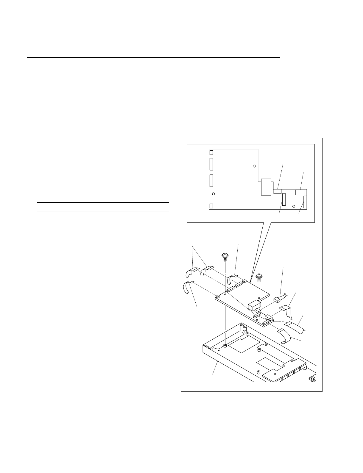
1-5. Replacing the Board
1-5-1. MB-978 Board
w
Before starting the replacement, be sure to pull out the
power plug from the wall outlet.
1. Remove the upper panel. (Refer to Section 1-1.)
2. Disconnect the flexible boards, cables, and harness
from the connectors on the MB-978 board.
Connector Quantity Cable
CN301, CN304, CN306 3 Flexible flat cable
CN501, CN502 2 TouchEngine board
CN303 1 SW-1098 flexible
board
CN305 1 Touch panel flexible
board
CN302 1 Harness
3. Remove the three screws, then remove the MB-978
board.
4. Remove the CPU-352 board. (Refer to Section 1-5-2.)
CN501
CN306
CN304
CN502
Flexible flat
cables
MB-978 board (Side B)
TouchEngine
board
PSW
3x6
CN302
CN303 CN301
Harness
PSW
3x6
Touch panel
flexible board
CN305
1-8 (E)
SW-1098
TouchEngine
board
Upper panel
flexible
board
Flexible
flat cable
5. Install the new MB-978 board in the reverse order of
steps 1 to 4.
UCP-8060
Page 17
1-5. Replacing the Board
CN501
CN303 CN305
CN502
MB-978 board (Side B)
CN306
LCD panel
assembly
MB-978 board
TouchEngine boards
Flexible flat
cable
Touch panel
flexible board
SW-1098
flexible board
PSW
3x6
PSW
3x6
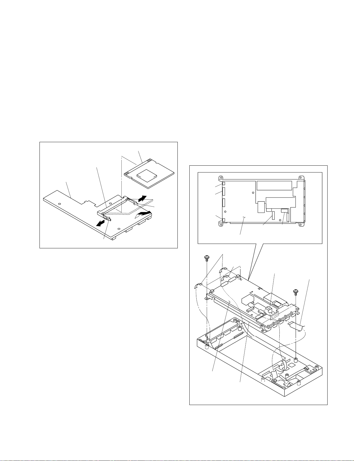
1-5-2. CPU-352 Board
w
Before starting the replacement, be sure to pull out the
power plug from the wall outlet.
1. Remove the upper panel. (Refer to Section 1-1.)
2. Remove the MB-978 board. (Refer to Section 1-5-1.)
3. Open the two hooks of the connector (CN102) on the
MB-978 board in the direction of the arrow A, then
remove the CPU-352 board in the direction of the
arrow B.
CPU-352 board
CN102
MB-978 board
A
Hook
1-5-3. TouchEngine Board
w
Before starting the replacement, be sure to pull out the
power plug from the wall outlet.
1. Remove the upper panel. (Refer to Section 1-1.)
2. Remove the two TouchEngine boards from the
connectors (CN501 and CN502), one flexible flat
cable from the connector (CN306), one touch panel
flexible board from the connector (CN305), and one
SW-1098 flexible board from the connector (CN303)
on the MB-978 board.
3. Remove the four screws, then remove the LCD panel
assembly.
A
Hook
B
4. Install a new CPU-352 board in the reverse order of
steps 1 to 3.
UCP-8060
1-9 (E)
Page 18
1-5. Replacing the Board
1-6. Replacing the Main Parts
4. Remove the two TouchEngine boards from the four
bosses.
Install the TouchEngine board with the
piezoelectric actuator side up.
TouchEngine board
TouchEngine board
Upper panel
Bosses
1-6. Replacing the Main Parts
1-6-1. Switching Regulator
w
Before starting the replacement, be sure to pull out the
power plug from the wall outlet.
n
Do not disassemble the switching regulator.
1. Remove the upper panel. (Refer to Section 1-1.)
2. Remove the two screws (B 3x6), then remove the heat
conducting plate.
3. Remove the two screws (M 3x8) and one screw (B
3x5), then remove the plate nut.
4. Remove the four screws (PSW 3x6), then remove the
PS-635 board.
Heat conducting plate
B
Boss
TouchEngine board
Boss
5. Install new TouchEngine boards in the reverse order of
steps 1 to 4.
m
. When installing the TouchEngine boards, make sure
to install them with the piezoelectric actuator side
up.
. Before attaching the LCD panel assembly, make
sure that the dust is not adhered to the surface of the
LCD panel and the backside of the touch panel.
Plate nut
A
B 3x5
A
PSW
3x6
M 3x8
B
PS-635
board
B 3x6
1-10 (E)
UCP-8060
Page 19
1-6. Replacing the Main Parts
VR-282 board
PSW 3x6
Volume knob assemblies
MB-978 board
CN306
Flexible flat cable
5. Remove the five solders fixing the switching regulator.
6. Remove the switching regulator from the PS-635
board.
Switching regulator
PS-635 board
Solders
7. Attach a new switching regulator in the reverse order
of steps 1 to 6.
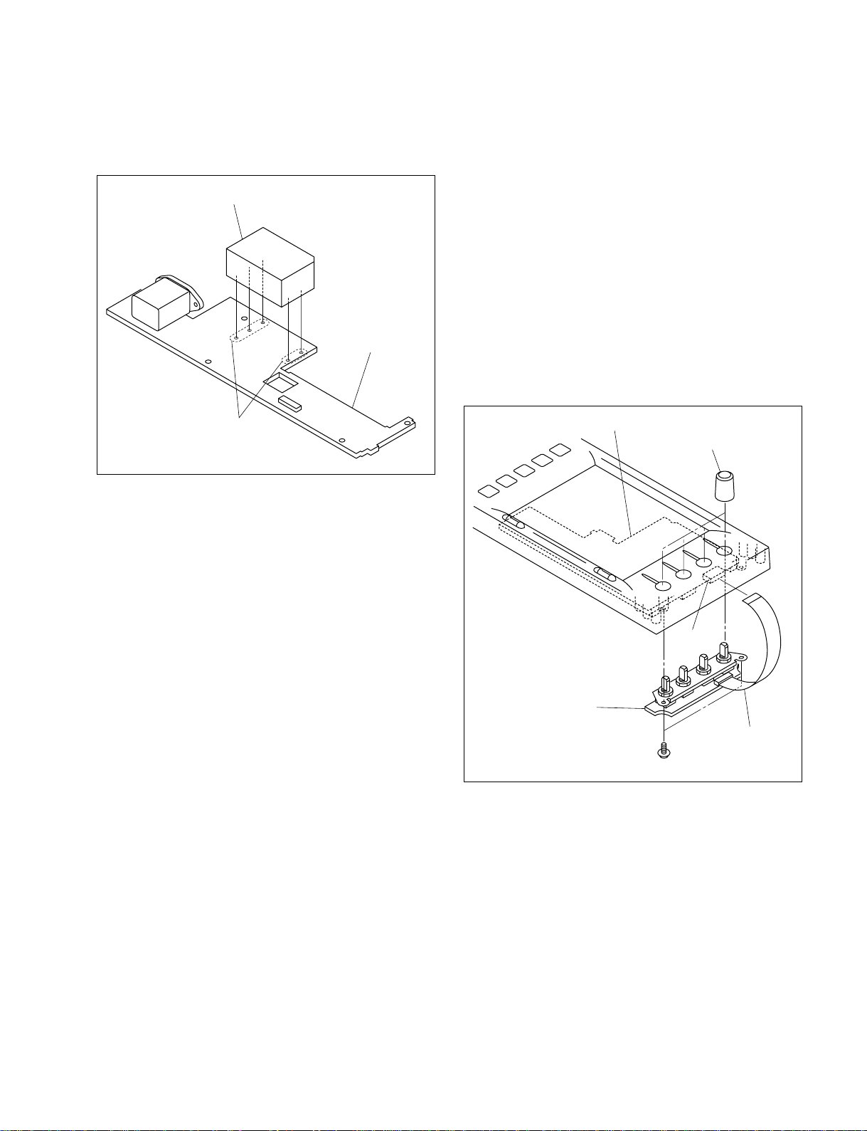
1-6-2. Rotary Encoder
w
Before starting the replacement, be sure to pull out the
power plug from the wall outlet.
1. Remove the upper panel. (Refer to Section 1-1.)
2. Remove the four volume knob assemblies.
n
Do not pull the volume knob assemblies by force.
Otherwise, it may damage the rotary encoders.
3. Disconnect one flexible flat cable from the connector
(CN306) on the MB-978 board.
4. Remove the two screws, then remove the VR-282
board.
UCP-8060
1-11 (E)
Page 20

1-6. Replacing the Main Parts
5. Remove the four nuts and four washers, then remove
the VR mounting plate.
6. Remove the solder from the VR-282 board, then
remove the rotary encoder.
VR mounting plate
Nut
Washer
Rotary encoders
Solder
VR-282 board
1-6-3. Inverter Unit
w
. Before starting the replacement, be sure to pull out the
power plug from the wall outlet.
. Do not start the replacement within 30 minutes after
turning off the power to avoid the electric shock or
injury.
1. Remove the upper panel. (Refer to Section 1-1.)
2. Disconnect the two harnesses from the connectors
(CN2 and CN3) on the inverter unit.
3. Remove the two screws, then remove the inverter unit.
4. Disconnect one harness from the inverter unit.
PSW
3x6
Harness
CN2
Inverter unit
CN3
7. Attach a new rotary encoders in the reverse order of
steps 1 to 6.
n
When attaching the rotary encoders, be sure to
temporarily secure them to the VR mounting plate
with nuts and washers before soldering to the VR-282
board.
Harnesses
MB-978 board
5. Attach a new inverter unit in the reverse order of steps
1 to 4.
1-12 (E)
UCP-8060
Page 21

1-6. Replacing the Main Parts
1-6-4. LCD Panel
w
Before starting the replacement, be sure to pull out the
power plug from the wall outlet.
1. Remove the upper panel. (Refer to Section 1-1.)
2. Remove the LCD panel assembly. (Refer to steps 1 to
3 of “1-5-3. TouchEngine Board”)
3. Disconnect one flexible flat cable from the connector
(CN301) on the MB-978 board.
4. Remove the three screws, then raise the MB-978
board.
5. Raise the two wire holders, then disconnect the two
harnesses from the connectors (CN2 and CN3) on the
inverter unit.
PSW
3x6
PSW
3x6
MB-978 board
CN301
Flexible
flat cable
6. Remove the four screws, then remove the LCD panel.
7. Remove the CN-2284 board from the LCD panel.
B 3x6
LCD panel
B 3x6
CN-2284
board
MB-978 board
Inverter unit
LCD panel assembly
Wire holder
Wire holder
CN2
CN3
Harnesses
8. Attach a new LCD panel in the reverse order of steps 1
to 7.
n
Before attaching the LCD panel assembly, make sure
that the dust is not adhered to the surface of the LCD
panel and the backside of the touch panel.
UCP-8060
1-13 (E)
Page 22

1-6. Replacing the Main Parts
1-6-5. Back Light
w
. Before starting the replacement, be sure to pull out the
power plug from the wall outlet.
. Do not start the replacement within 30 minutes after
turning off the power to avoid the electric shock or
injury.
n
When replacing, replace the two back lights at the same
time.
1. Perform steps 1 to 5 of Section 1-6-4.
2. Pull out the two back lights while pushing the two
stoppers of the LCD panel in the direction of the arrow
A.
1-6-6. Touch Panel
w
Before starting the replacement, be sure to pull out the
power plug from the wall outlet.
1. Remove the upper panel. (Refer to Section 1-1.)
2. Remove the LCD panel assembly and TouchEngine
board. (Refer to Section 1-5-3.)
3. Remove the touch panel.
Touch panel
Tape side
Guides
Guides
A
Stopper
A
LCD panel
Stopper
Back light
Back light
3. Attach new back lights in the reverse procedure.
n
Before attaching the LCD panel assembly, make sure
that the dust is not adhered to the surface of the LCD
panel and the backside of the touch panel.
Upper panel
4. Attach a new touch panel in the reverse order of steps
1 to 3.
m
. Make sure to attach the touch panel with the tape
(affixed to the touch panel flexible board) side up.
. Attach the touch panel along the guides of the upper panel
and make sure that the touch panel is securely attached.
. After installing the touch panel flexible board to the
connector (CN305) on the MB-978 board, put a crease in
the board.
(Refer to Fig. 1.)
. Before attaching the LCD panel assembly, make sure
that the dust is not adhered to the surface of the LCD
panel and the backside of the touch panel.
1-14 (E)
UCP-8060
Page 23

1-6. Replacing the Main Parts
# Welcome to BIOS SETUP UTILITY for UCP-8060 vx.xx
>
BIOS
UTILITY of
version
1-7. Replacing the Fuse/IC Link
1-8. Initializing System Setting Value
Fig. 1
CN305
MB-978 board
Put a crease.
2-4 mm
Touch panel
flexible board
1-7. Replacing the Fuse/IC Link
w
A fuse and IC link are critical parts to safe operation.
Replace this component with Sony parts whose part
numbers appear in this manual published by Sony.
If not, this may cause a fire or electric shock.
Be sure to use the specified component in this manual.
The fuses and IC links are mounted on the boards below.
Be sure to replace with the specified fuse and IC link as
shown below after removing the foreign substances that
may cause the shorts.
PS-635 board
1-8. Initializing System Setting Value
Following are the items to be initialized.
. Calibration data of touch panel
n
The unit always enters the calibration input mode at the
first startup after the initialization of system setting
value. This is because of the specification of operation
software and is not a problem.
. DEVICE CONTROL DATA file (brightness of LCD
back light, brightness of function switch, buzzer sound
volume, TouchEngine sensitivity and touch buzzer
sound off/on)
. TCP/IP setting value
Perform this initialization also when the MAC address
written in the flash memory (IC203/CPU-352 board) is
damaged, it is automatically restored based on the data
backed up in EEPROM (IC204/CPU-352 board).
Required equipment
. PC (with terminal software installed)
. RS-232C cross cable
Procedure
1. Connect the PC and the RS-232C connector of the
UCP-8060 using the RS-232C cross cable.
2. Turn on the power of the PC to start the terminal
software.
3. Set the communication conditions as follows;
Ref No. (Address) Description Parts No.
F101 (B-2) H.B.C. Fuse !1-576-228-11
PS101 (F-2) Circuit Protector !1-533-282-21
IC link 2 A
UCP-8060
Baud rate 9600
Data 8 bit
Parity None
Stop 1 bit
Flow control None
4. Start the BIOS UTILITY of the UCP-8060. (For
startup procedure, refer to the “Basic Operations”
(Confirmation of the basic information) in the
operation manual.)
Following message appears on the terminal screen.
1-15 (E)
Page 24

1-8. Initializing System Setting Value
1-9. System File Recovery
5. Type “factory” from the keyboard of the PC.
6. Press the Enter key.
The initialization starts. When it is completed, the
following message is displayed on the terminal screen.
Remove setup files for factory mode... OK
7. Terminate the terminal software.
1-9. System File Recovery
Required equipment
. PC that can copy files to the Memory Stick
. Boot-up MultiMediaCard (MMC)
For the procedure to make the boot-up MMC, refer to
Section 2-5 of the installation manual.
. Memory Stick (with nothing is written)
. System file
. Operation software (to be reinstalled after system file
recovery)
To obtain the system file and operation software, contact
your local Sony Sales Office/Service Center.
Memory Stick slot
Function button 2
Select L button
Select R button
Preparation
1. Format the Memory Stick. (Refer to the operation
manual.)
2. Turn on the power of the PC.
3. Copy the system file to any place of the PC.
4. Double-click the system file to uncompress it.
The uncompressed data is stored in the following
directory.
MSSONY/PRO/UCP
5. Insert the Memory Stick formatted in step 1 into the
PC.
6. Copy the folder including the data uncompressed in
step 4 to the Memory Stick.
7. Pull out the Memory Stick from the PC.
1-16 (E)
UCP-8060
Page 25

Installation (Update)
1. Remove the six screws, then open the upper panel.
n
Do not disconnect the flexible flat cable connecting the
PS-635 board and the MB-978 board.
2. Check that S201 (D-1) on the MB-798 board is set to
ON.
3. Insert the boot-up MMC to the CN201 (D-1) on the
MB-978 board.
4. Close the upper panel. (Securing with screws is not
required.)
5. Turn on the power of the UCP-8060.
6. While pressing the function button 2, press the select L
and R buttons simultaneously for more than three
seconds.
When the function button 2 lights on, release all
buttons.
7. Insert the Memory Stick in which the system file is
written into the Memory Stick slot of the UCP-8060.
8. Press the select R button according to the instruction
on the screen.
Updating of the system file starts.
9. Check that the message to indicate the completion of
updating is displayed on the screen.
10. Pull out the Memory Stick from the Memory Stick
slot.
11. Turn off the power of the UCP-8060.
12. Open the upper panel and pull out the boot-up MMC.
13. Close the upper panel.
1-9. System File Recovery
Operation check
1. Turn on the power of the UCP-8060.
2. Check that the Main screen is displayed.
If the Main screen is displayed, it means that the
system file is recovered.
n
In case that the Main screen is not displayed, the
hardware may be damaged.
Refer to “Although the back light is lit, nothing is
displayed on the liquid crystal panel” in “1-4.
Troubleshooting”.
3. Attach the upper panel with the six screws.
4. Install the operation software as required. (Refer to the
operation manual.)
UCP-8060
1-17 (E)
Page 26

Page 27

Section 2
Spare Parts
2-1. Notes on Repair Parts
1. Safety Related Components Warning
w
Components marked ! are critical to safe operation.
Therefore, specified parts should be used in the case of
replacement.
2. Standardization of Parts
Some repair parts supplied by Sony differ from those
used for the unit. These are because of parts commonality and improvement.
Parts list has the present standardized repair parts.
3. Stock of Parts
Parts marked with “o” at SP (Supply Code) column of
the spare parts list may not be stocked. Therefore, the
delivery date will be delayed.
4. Harness
Harnesses with no part number are not registered as
spare parts.
In need of repair, get components shown in the list and
repair using them.
2-1.
UCP-8060
2-1
Page 28

Lower Panel Block
2-2. Exploded Views
3
B
A
6
1
4
PSW 3x6
2
PS-635
Board
B 4x6
A
B
B 3x5
No. Part No. SP Description
B 3x5
1 ! 1-468-486-11 s REGULATOR, SWITCHING (KWS15-5)
2 1-757-644-11 s CABLE, FLEXIBLE FLAT (30 CORE)
3 ! 1-794-141-11 s INLET (WITH NOISE FILTER)
4 3-364-990-01 s SCREW (M3X8)
5 3-370-475-01 s SCREW (+B) (3X6),NYLOCK
6 3-629-592-02 o RUBBER (PR), RADIATION
7-682-546-09 s SCREW +B3X5
7-682-560-09 s SCREW +B4X6
7-682-947-01 s SCREW +PSW 3X6
2-2
5
B 3x5
B 4x6
UCP-8060
Page 29

LED-397
Board
Front Panel Block
PSW 3x6
SW-1099
Board
104
A
SW-1098
Board
PSW 3x6
102
101
104
B
PSW
3x6
103
PSW 3x6
A
PSW 3x6
No. Part No. SP Description
101 X-3608-487-1 s ASSY,VOLUME KNOB
102 1-417-337-11 s PANEL, TOUCH
103 1-477-701-11 s ENCODER TYPE, OPTICS
104 1-761-651-11 s PWB, MOUNTED
105 1-823-558-11 s CABLE, FLEXIBLE FLAT (30CORE)
7-682-947-01 s SCREW +PSW 3X6
B
PSW 3x6
VR-282
Board
105
UCP-8060
2-3
Page 30

LCD Block
209
PSW 3x6
203
207
B 3x6
205
PSW
3x6
207
B 3x6
208
CN-2284
Board
PSW 3x6
KY-537
Board
PSW 3x6
204
PSW 3x6
202
No. Part No. SP Description
201 A-8345-525-A s MOUNTED CIRCUIT BOARD, CPU-352
202 A-8345-526-A s MOUNTED CIRCUIT BOARD, MB-978
203 ! 1-477-607-11 s INVERTER UNIT (LCD MODULE)
204 1-757-273-11 s CABLE, FLEXIBLE FLAT (30 CORE)
205 1-805-059-11 s LCD MODULE
206 1-823-558-11 s CABLE, FLEXIBLE FLAT (30CORE)
207 3-701-822-00 s HOLDER, WIRE
208 4-908-723-11 o SPACER (1)
209 9-885-028-72 s BACK LIGHT
201
206
7-682-547-04 s SCREW +B3X6
7-682-947-01 s SCREW +PSW 3X6
2-4
UCP-8060
Page 31

2-3. Electrical Parts List
------------CN-2284 BOARD
------------ Ref. No.
or Q'ty Part No. SP Description
CN304 1-573-370-21 s CONNECTOR, FFC/FPC 30P
------------CPU-352 BOARD
------------ Ref. No.
or Q'ty Part No. SP Description
1pc A-8345-525-A s MOUNTED CIRCUIT BOARD, CPU-352
CN801 1-779-396-11 o CONNECTOR, BOARD TO BOARD 31P
C201 1-107-826-11 s CAPACITOR,CHIP CERAMIC 0.1MF
C202 1-107-826-11 s CAPACITOR,CHIP CERAMIC 0.1MF
C203 1-162-923-11 s CAPACITOR,CERAMIC 47PF/50V CH
C205 1-162-923-11 s CAPACITOR,CERAMIC 47PF/50V CH
C206 1-162-970-11 s CAPACITOR CERAMIC 0.01MF/25V B
C207 1-162-970-11 s CAPACITOR CERAMIC 0.01MF/25V B
C208 1-162-970-11 s CAPACITOR CERAMIC 0.01MF/25V B
C210 1-162-970-11 s CAPACITOR CERAMIC 0.01MF/25V B
C211 1-162-919-11 s CAPACITOR,CERAMIC 22PF/50V CH
C212 1-162-970-11 s CAPACITOR CERAMIC 0.01MF/25V B
C214 1-162-970-11 s CAPACITOR CERAMIC 0.01MF/25V B
C215 1-162-919-11 s CAPACITOR,CERAMIC 22PF/50V CH
C216 1-162-970-11 s CAPACITOR CERAMIC 0.01MF/25V B
C217 1-162-970-11 s CAPACITOR CERAMIC 0.01MF/25V B
C218 1-162-970-11 s CAPACITOR CERAMIC 0.01MF/25V B
C219 1-162-970-11 s CAPACITOR CERAMIC 0.01MF/25V B
C220 1-162-970-11 s CAPACITOR CERAMIC 0.01MF/25V B
C221 1-162-970-11 s CAPACITOR CERAMIC 0.01MF/25V B
C222 1-162-970-11 s CAPACITOR CERAMIC 0.01MF/25V B
C223 1-162-970-11 s CAPACITOR CERAMIC 0.01MF/25V B
C224 1-162-970-11 s CAPACITOR CERAMIC 0.01MF/25V B
C225 1-162-970-11 s CAPACITOR CERAMIC 0.01MF/25V B
C227 1-126-391-11 s CAPACITOR ELECT 47MF/6.3V(105)
C228 1-162-970-11 s CAPACITOR CERAMIC 0.01MF/25V B
C229 1-162-970-11 s CAPACITOR CERAMIC 0.01MF/25V B
C230 1-162-970-11 s CAPACITOR CERAMIC 0.01MF/25V B
C231 1-162-970-11 s CAPACITOR CERAMIC 0.01MF/25V B
C232 1-162-970-11 s CAPACITOR CERAMIC 0.01MF/25V B
C233 1-162-970-11 s CAPACITOR CERAMIC 0.01MF/25V B
C234 1-162-970-11 s CAPACITOR CERAMIC 0.01MF/25V B
C235 1-162-970-11 s CAPACITOR CERAMIC 0.01MF/25V B
C236 1-107-826-11 s CAPACITOR,CHIP CERAMIC 0.1MF
C301 1-126-391-11 s CAPACITOR ELECT 47MF/6.3V(105)
C302 1-162-970-11 s CAPACITOR CERAMIC 0.01MF/25V B
C303 1-126-391-11 s CAPACITOR ELECT 47MF/6.3V(105)
C304 1-162-970-11 s CAPACITOR CERAMIC 0.01MF/25V B
C305 1-162-970-11 s CAPACITOR CERAMIC 0.01MF/25V B
C306 1-162-970-11 s CAPACITOR CERAMIC 0.01MF/25V B
C307 1-162-970-11 s CAPACITOR CERAMIC 0.01MF/25V B
C308 1-162-970-11 s CAPACITOR CERAMIC 0.01MF/25V B
C309 1-162-970-11 s CAPACITOR CERAMIC 0.01MF/25V B
C310 1-162-970-11 s CAPACITOR CERAMIC 0.01MF/25V B
C311 1-162-970-11 s CAPACITOR CERAMIC 0.01MF/25V B
C312 1-162-970-11 s CAPACITOR CERAMIC 0.01MF/25V B
C313 1-162-970-11 s CAPACITOR CERAMIC 0.01MF/25V B
C314 1-162-970-11 s CAPACITOR CERAMIC 0.01MF/25V B
C315 1-162-970-11 s CAPACITOR CERAMIC 0.01MF/25V B
C316 1-162-970-11 s CAPACITOR CERAMIC 0.01MF/25V B
C317 1-162-970-11 s CAPACITOR CERAMIC 0.01MF/25V B
C318 1-162-970-11 s CAPACITOR CERAMIC 0.01MF/25V B
C319 1-162-970-11 s CAPACITOR CERAMIC 0.01MF/25V B
C320 1-162-970-11 s CAPACITOR CERAMIC 0.01MF/25V B
C321 1-162-970-11 s CAPACITOR CERAMIC 0.01MF/25V B
C322 1-162-970-11 s CAPACITOR CERAMIC 0.01MF/25V B
C323 1-162-970-11 s CAPACITOR CERAMIC 0.01MF/25V B
UCP-8060
C324 1-162-970-11 s CAPACITOR CERAMIC 0.01MF/25V B
2-5
Page 32

(CPU-352 BOARD)
Ref. No.
or Q'ty Part No. SP Description
-----------KY-537 BOARD
----------- Ref. No.
or Q'ty Part No. SP Description
IC201 8-759-584-62 s IC RQ5RW28BA-TR
CN301 1-573-370-21 s CONNECTOR, FFC/FPC 30P
IC202 6-703-172-01 s IC IM100-TQ144C
IC203 6-703-134-01 s IC AT45DB321B-TI
IC204 8-759-678-06 s IC CAT24WC02JI-TE13
IC205 8-759-699-62 s IC MT4LC4M16R6TG-5TR
Q301 8-729-014-45 s TRANSISTOR RN1905-TE85R
Q302 8-729-014-45 s TRANSISTOR RN1905-TE85R
Q303 8-729-014-45 s TRANSISTOR RN1905-TE85R
Q304 8-729-014-45 s TRANSISTOR RN1905-TE85R
IC206 8-759-699-62 s IC MT4LC4M16R6TG-5TR
Q305 8-729-014-45 s TRANSISTOR RN1905-TE85R
IC301 6-702-658-01 s IC XC2S150-5PQ208C1
IC302 8-759-548-95 s IC SN74LV00APWR
R301 1-211-969-11 s RESISTOR,CHIP 10 1/10W (1608)
R302 1-211-977-11 s RESISTOR,CHIP 22 1/10W (1608)
L201 1-414-170-41 s INDUCTOR, CHIP 100UH (2012)
R303 1-218-823-11 s RESISTOR,CHIP 100 1/10W (1608)
R304 1-211-977-11 s RESISTOR,CHIP 22 1/10W (1608)
R203 1-218-863-11 s RESISTOR,CHIP 4.7K 1/10W(1608)
R305 1-211-969-11 s RESISTOR,CHIP 10 1/10W (1608)
R204 1-216-857-11 s RESISTOR,CHIP 1M 1/10W(1608)
R205 1-218-863-11 s RESISTOR,CHIP 4.7K 1/10W(1608)
R206 1-211-977-11 s RESISTOR,CHIP 22 1/10W (1608)
R207 1-218-863-11 s RESISTOR,CHIP 4.7K 1/10W(1608)
R306 1-211-977-11 s RESISTOR,CHIP 22 1/10W (1608)
R307 1-218-823-11 s RESISTOR,CHIP 100 1/10W (1608)
R308 1-211-977-11 s RESISTOR,CHIP 22 1/10W (1608)
R309 1-211-969-11 s RESISTOR,CHIP 10 1/10W (1608)
R209 1-218-863-11 s RESISTOR,CHIP 4.7K 1/10W(1608)
R310 1-211-977-11 s RESISTOR,CHIP 22 1/10W (1608)
R210 1-218-863-11 s RESISTOR,CHIP 4.7K 1/10W(1608)
R211 1-218-863-11 s RESISTOR,CHIP 4.7K 1/10W(1608)
R212 1-218-863-11 s RESISTOR,CHIP 4.7K 1/10W(1608)
R213 1-218-863-11 s RESISTOR,CHIP 4.7K 1/10W(1608)
R311 1-218-823-11 s RESISTOR,CHIP 100 1/10W (1608)
R312 1-211-977-11 s RESISTOR,CHIP 22 1/10W (1608)
R313 1-211-969-11 s RESISTOR,CHIP 10 1/10W (1608)
R314 1-211-977-11 s RESISTOR,CHIP 22 1/10W (1608)
R308 1-211-977-11 s RESISTOR,CHIP 22 1/10W (1608)
R315 1-218-823-11 s RESISTOR,CHIP 100 1/10W (1608)
R309 1-211-977-11 s RESISTOR,CHIP 22 1/10W (1608)
R310 1-211-977-11 s RESISTOR,CHIP 22 1/10W (1608)
R311 1-211-977-11 s RESISTOR,CHIP 22 1/10W (1608)
R316 1-211-977-11 s RESISTOR,CHIP 22 1/10W (1608)
R317 1-211-969-11 s RESISTOR,CHIP 10 1/10W (1608)
R318 1-211-977-11 s RESISTOR,CHIP 22 1/10W (1608)
X201 1-760-622-21 s VIBRATOR, CRYSTAL
X202 1-781-204-11 s VIBRATOR, CRYSTAL
R319 1-218-823-11 s RESISTOR,CHIP 100 1/10W (1608)
R320 1-211-977-11 s RESISTOR,CHIP 22 1/10W (1608)
S301 1-786-251-11 s SWITCH, TACTILE
S302 1-786-251-11 s SWITCH, TACTILE
S303 1-786-251-11 s SWITCH, TACTILE
S304 1-786-251-11 s SWITCH, TACTILE
S305 1-786-251-11 s SWITCH, TACTILE
2-6
-------------
LED-397 BOARD
-------------
Ref. No.
or Q'ty Part No. SP Description
CN601 1-691-346-11 s CONNECTOR, FFC/FPC 8P
D601 8-719-073-33 s DIODE CL-165HR/YG-D-T
D602 8-719-073-33 s DIODE CL-165HR/YG-D-T
UCP-8060
Page 33

-----------MB-978 BOARD
----------- Ref. No.
or Q'ty Part No. SP Description
(MB-978 BOARD)
Ref. No.
or Q'ty Part No. SP Description
1pc A-8345-526-A s MOUNTED CIRCUIT BOARD, MB-978
C305 1-162-966-11 s CAPACITOR,CERAMIC 2200PF/50V B
C306 1-126-391-11 s CAPACITOR ELECT 47MF/6.3V(105)
C101 1-165-603-11 s CAPACITOR DOUBLE LAYERS 1.5F
C103 1-126-391-11 s CAPACITOR ELECT 47MF/6.3V(105)
C105 1-107-826-11 s CAPACITOR,CHIP CERAMIC 0.1MF
C307 1-126-391-11 s CAPACITOR ELECT 47MF/6.3V(105)
C308 1-107-826-11 s CAPACITOR,CHIP CERAMIC 0.1MF
C309 1-107-826-11 s CAPACITOR,CHIP CERAMIC 0.1MF
C106 1-126-391-11 s CAPACITOR ELECT 47MF/6.3V(105)
C107 1-107-826-11 s CAPACITOR,CHIP CERAMIC 0.1MF
C310 1-107-826-11 s CAPACITOR,CHIP CERAMIC 0.1MF
C311 1-162-966-11 s CAPACITOR,CERAMIC 2200PF/50V B
C108 1-107-826-11 s CAPACITOR,CHIP CERAMIC 0.1MF
C109 1-107-826-11 s CAPACITOR,CHIP CERAMIC 0.1MF
C110 1-107-826-11 s CAPACITOR,CHIP CERAMIC 0.1MF
C312 1-126-391-11 s CAPACITOR ELECT 47MF/6.3V(105)
C313 1-162-966-11 s CAPACITOR,CERAMIC 2200PF/50V B
C314 1-162-966-11 s CAPACITOR,CERAMIC 2200PF/50V B
C111 1-107-826-11 s CAPACITOR,CHIP CERAMIC 0.1MF
C112 1-107-826-11 s CAPACITOR,CHIP CERAMIC 0.1MF
C315 1-162-966-11 s CAPACITOR,CERAMIC 2200PF/50V B
C401 1-162-970-11 s CAPACITOR CERAMIC 0.01MF/25V B
C113 1-126-391-11 s CAPACITOR ELECT 47MF/6.3V(105)
C114 1-126-391-11 s CAPACITOR ELECT 47MF/6.3V(105)
C115 1-107-826-11 s CAPACITOR,CHIP CERAMIC 0.1MF
C402 1-162-919-11 s CAPACITOR,CERAMIC 22PF/50V CH
C403 1-162-919-11 s CAPACITOR,CERAMIC 22PF/50V CH
C404 1-162-970-11 s CAPACITOR CERAMIC 0.01MF/25V B
C116 1-107-826-11 s CAPACITOR,CHIP CERAMIC 0.1MF
C117 1-107-826-11 s CAPACITOR,CHIP CERAMIC 0.1MF
C405 1-162-970-11 s CAPACITOR CERAMIC 0.01MF/25V B
C406 1-162-970-11 s CAPACITOR CERAMIC 0.01MF/25V B
C118 1-107-826-11 s CAPACITOR,CHIP CERAMIC 0.1MF
C119 1-107-826-11 s CAPACITOR,CHIP CERAMIC 0.1MF
C120 1-107-826-11 s CAPACITOR,CHIP CERAMIC 0.1MF
C407 1-126-391-11 s CAPACITOR ELECT 47MF/6.3V(105)
C408 1-164-230-11 s CAPACITOR,CERAMIC 220PF/50V
C409 1-164-230-11 s CAPACITOR,CERAMIC 220PF/50V
C201 1-107-826-11 s CAPACITOR,CHIP CERAMIC 0.1MF
C203 1-107-826-11 s CAPACITOR,CHIP CERAMIC 0.1MF
C410 1-107-826-11 s CAPACITOR,CHIP CERAMIC 0.1MF
C411 1-162-923-11 s CAPACITOR,CERAMIC 47PF/50V CH
C204 1-126-391-11 s CAPACITOR ELECT 47MF/6.3V(105)
C205 1-107-826-11 s CAPACITOR,CHIP CERAMIC 0.1MF
C206 1-107-826-11 s CAPACITOR,CHIP CERAMIC 0.1MF
C412 1-162-970-11 s CAPACITOR CERAMIC 0.01MF/25V B
C413 1-162-923-11 s CAPACITOR,CERAMIC 47PF/50V CH
C414 1-126-391-11 s CAPACITOR ELECT 47MF/6.3V(105)
C207 1-107-826-11 s CAPACITOR,CHIP CERAMIC 0.1MF
C208 1-107-826-11 s CAPACITOR,CHIP CERAMIC 0.1MF
C415 1-107-826-11 s CAPACITOR,CHIP CERAMIC 0.1MF
C501 1-107-826-11 s CAPACITOR,CHIP CERAMIC 0.1MF
C209 1-107-826-11 s CAPACITOR,CHIP CERAMIC 0.1MF
C210 1-107-826-11 s CAPACITOR,CHIP CERAMIC 0.1MF
C211 1-107-826-11 s CAPACITOR,CHIP CERAMIC 0.1MF
C502 1-107-826-11 s CAPACITOR,CHIP CERAMIC 0.1MF
C503 1-107-826-11 s CAPACITOR,CHIP CERAMIC 0.1MF
C504 1-165-872-11 s CAPACITOR,SOLID ELECT 47MF
C212 1-107-826-11 s CAPACITOR,CHIP CERAMIC 0.1MF
C213 1-107-826-11 s CAPACITOR,CHIP CERAMIC 0.1MF
C506 1-107-420-11 s CAPACITOR,ELECT 47MF/35V(105C)
C507 1-107-420-11 s CAPACITOR,ELECT 47MF/35V(105C)
C214 1-107-826-11 s CAPACITOR,CHIP CERAMIC 0.1MF
C215 1-107-826-11 s CAPACITOR,CHIP CERAMIC 0.1MF
C216 1-107-826-11 s CAPACITOR,CHIP CERAMIC 0.1MF
C508 1-162-923-11 s CAPACITOR,CERAMIC 47PF/50V CH
C509 1-162-923-11 s CAPACITOR,CERAMIC 47PF/50V CH
C511 1-107-826-11 s CAPACITOR,CHIP CERAMIC 0.1MF
C217 1-107-826-11 s CAPACITOR,CHIP CERAMIC 0.1MF
C218 1-107-826-11 s CAPACITOR,CHIP CERAMIC 0.1MF
C512 1-107-826-11 s CAPACITOR,CHIP CERAMIC 0.1MF
C513 1-165-872-11 s CAPACITOR,SOLID ELECT 47MF
C219 1-107-826-11 s CAPACITOR,CHIP CERAMIC 0.1MF
C220 1-107-826-11 s CAPACITOR,CHIP CERAMIC 0.1MF
C221 1-107-826-11 s CAPACITOR,CHIP CERAMIC 0.1MF
C222 1-107-826-11 s CAPACITOR,CHIP CERAMIC 0.1MF
C223 1-107-826-11 s CAPACITOR,CHIP CERAMIC 0.1MF
CN101 1-573-370-21 s CONNECTOR, FFC/FPC 30P
CN102 1-785-948-12 s HINGE LEFT 14G-NI
CN301 1-573-370-21 s CONNECTOR, FFC/FPC 30P
CN302 1-580-789-21 o PIN,CONNECTOR (SMD) 6P
CN303 1-573-370-21 s CONNECTOR, FFC/FPC 30P
C224 1-107-826-11 s CAPACITOR,CHIP CERAMIC 0.1MF
C225 1-107-826-11 s CAPACITOR,CHIP CERAMIC 0.1MF
C226 1-107-826-11 s CAPACITOR,CHIP CERAMIC 0.1MF
C227 1-107-826-11 s CAPACITOR,CHIP CERAMIC 0.1MF
C228 1-107-826-11 s CAPACITOR,CHIP CERAMIC 0.1MF
CN304 1-573-370-21 s CONNECTOR, FFC/FPC 30P
CN305 1-793-708-21 s CONNECTOR, FLEXIBLE 8P
CN306 1-573-370-21 s CONNECTOR, FFC/FPC 30P
CN401 1-817-173-11 s JACK, MODULAR (WITH LED, PT)8P
CN402 1-778-551-11 o PIN, CONNECTOR 20P
C229 1-107-826-11 s CAPACITOR,CHIP CERAMIC 0.1MF
C230 1-107-826-11 s CAPACITOR,CHIP CERAMIC 0.1MF
C231 1-107-826-11 s CAPACITOR,CHIP CERAMIC 0.1MF
CN501 1-691-346-11 s CONNECTOR, FFC/FPC 8P
CN502 1-691-346-11 s CONNECTOR, FFC/FPC 8P
C232 1-107-826-11 s CAPACITOR,CHIP CERAMIC 0.1MF
C233 1-107-826-11 s CAPACITOR,CHIP CERAMIC 0.1MF
D102 8-719-036-80 s DIODE RD3.9SB
D201 8-719-064-52 s DIODE CL-191YG-CD-T
C234 1-107-826-11 s CAPACITOR,CHIP CERAMIC 0.1MF
C236 1-107-826-11 s CAPACITOR,CHIP CERAMIC 0.1MF
C237 1-107-826-11 s CAPACITOR,CHIP CERAMIC 0.1MF
D202 8-719-071-10 s DIODE CL-191HR-CD-T
D301 8-719-989-00 s DIODE DA221
D302 8-719-420-90 s DIODE MA8051-M
C301 1-107-826-11 s CAPACITOR,CHIP CERAMIC 0.1MF
C302 1-107-826-11 s CAPACITOR,CHIP CERAMIC 0.1MF
D303 8-719-420-90 s DIODE MA8051-M
D304 8-719-420-90 s DIODE MA8051-M
C303 1-107-826-11 s CAPACITOR,CHIP CERAMIC 0.1MF
C304 1-107-826-11 s CAPACITOR,CHIP CERAMIC 0.1MF
D305 8-719-420-90 s DIODE MA8051-M
D306 8-719-420-90 s DIODE MA8051-M
UCP-8060
2-7
Page 34

(MB-978 BOARD)
(MB-978 BOARD)
Ref. No.
or Q'ty Part No. SP Description
D307 8-719-420-90 s DIODE MA8051-M
D308 8-719-420-90 s DIODE MA8051-M
D309 8-719-420-90 s DIODE MA8051-M
D501 8-719-048-98 s DIODE RB160L-40TE25
Ref. No.
or Q'ty Part No. SP Description
R305 1-218-855-11 s RESISTOR,CHIP 2.2K 1/10W(1608)
R306 1-218-863-11 s RESISTOR,CHIP 4.7K 1/10W(1608)
R307 1-218-871-11 s RESISTOR,CHIP 10K 1/10W (1608)
R308 1-218-871-11 s RESISTOR,CHIP 10K 1/10W (1608)
R309 1-218-839-11 s RESISTOR,CHIP 470 1/10W (1608)
FB301 1-414-444-11 s MICRO INDUCTOR (CHIP TYPE)
FB302 1-414-444-11 s MICRO INDUCTOR (CHIP TYPE)
FB303 1-414-444-11 s MICRO INDUCTOR (CHIP TYPE)
FB304 1-414-444-11 s MICRO INDUCTOR (CHIP TYPE)
FB401 1-414-444-11 s MICRO INDUCTOR (CHIP TYPE)
R310 1-218-847-11 s RESISTOR, CHIP 1K 1/10W (1608)
R311 1-218-855-11 s RESISTOR,CHIP 2.2K 1/10W(1608)
R312 1-218-847-11 s RESISTOR, CHIP 1K 1/10W (1608)
R313 1-218-855-11 s RESISTOR,CHIP 2.2K 1/10W(1608)
R314 1-218-855-11 s RESISTOR,CHIP 2.2K 1/10W(1608)
FB402 1-414-444-11 s MICRO INDUCTOR (CHIP TYPE)
R315 1-218-887-11 s RESISTOR,CHIP 47K 1/10W (1608)
IC101 8-759-460-72 s IC BA033FP
IC102 6-700-394-01 s IC BA25BC0FP-TE2
IC201 8-759-523-84 s IC TC74VHC14FT (EL)
IC202 6-702-658-01 s IC XC2S150-5PQ208C1
R316 1-218-887-11 s RESISTOR,CHIP 47K 1/10W (1608)
R317 1-218-855-11 s RESISTOR,CHIP 2.2K 1/10W(1608)
R318 1-218-823-11 s RESISTOR,CHIP 100 1/10W (1608)
R319 1-218-855-11 s RESISTOR,CHIP 2.2K 1/10W(1608)
IC203 8-759-557-51 s IC RN5VD30AA-TL
R320 1-218-831-11 s RESISTOR, CHIP 220 1/10W(1608)
IC204 8-759-091-93 s IC TLC555CPS
IC301 8-759-337-40 s IC NJM2904V(TE2)
IC302 8-759-549-22 s IC SN74LV574APWR
IC303 8-759-549-22 s IC SN74LV574APWR
R321 1-218-847-11 s RESISTOR, CHIP 1K 1/10W (1608)
R323 1-218-839-11 s RESISTOR,CHIP 470 1/10W (1608)
R324 1-218-847-11 s RESISTOR, CHIP 1K 1/10W (1608)
R325 1-218-839-11 s RESISTOR,CHIP 470 1/10W (1608)
IC304 8-759-248-78 s IC MB88102PFV-G-BND-ER
R326 1-218-847-11 s RESISTOR, CHIP 1K 1/10W (1608)
IC305 8-759-548-95 s IC SN74LV00APWR
IC401 6-703-185-01 s IC LXT971ALC
IC501 8-759-245-52 s IC TA7291F
IC502 8-759-455-17 s IC MAX1771CSA-TP
R327 1-218-871-11 s RESISTOR,CHIP 10K 1/10W (1608)
R328 1-218-871-11 s RESISTOR,CHIP 10K 1/10W (1608)
R329 1-218-871-11 s RESISTOR,CHIP 10K 1/10W (1608)
R330 1-218-871-11 s RESISTOR,CHIP 10K 1/10W (1608)
L501 1-416-345-11 s COIL, CHOKE 22UH
R331 1-218-871-11 s RESISTOR,CHIP 10K 1/10W (1608)
R332 1-218-871-11 s RESISTOR,CHIP 10K 1/10W (1608)
Q101 8-729-928-19 s TRANSISTOR 2SA1774R
Q102 8-729-929-08 s TRANSISTOR DTC123JE
Q201 8-729-928-54 s TRANSISTOR DTA123JE
R333 1-218-871-11 s RESISTOR,CHIP 10K 1/10W (1608)
R334 1-218-871-11 s RESISTOR,CHIP 10K 1/10W (1608)
R335 1-218-871-11 s RESISTOR,CHIP 10K 1/10W (1608)
Q301 8-729-929-08 s TRANSISTOR DTC123JE
Q302 8-729-928-54 s TRANSISTOR DTA123JE
R336 1-218-879-11 s RESISTOR,CHIP 22K 1/10W (1608)
R337 1-218-879-11 s RESISTOR,CHIP 22K 1/10W (1608)
Q501 8-729-044-58 s TRANSISTOR SI2304DS-T1
Q502 8-729-044-58 s TRANSISTOR SI2304DS-T1
Q503 8-729-928-54 s TRANSISTOR DTA123JE
R401 1-218-871-11 s RESISTOR,CHIP 10K 1/10W (1608)
R402 1-211-977-11 s RESISTOR,CHIP 22 1/10W (1608)
R403 1-216-857-11 s RESISTOR,CHIP 1M 1/10W(1608)
Q504 8-729-928-54 s TRANSISTOR DTA123JE
Q505 8-729-044-58 s TRANSISTOR SI2304DS-T1
R404 1-218-839-11 s RESISTOR,CHIP 470 1/10W (1608)
R405 1-218-839-11 s RESISTOR,CHIP 470 1/10W (1608)
Q506 8-729-929-08 s TRANSISTOR DTC123JE
R406 1-218-871-11 s RESISTOR,CHIP 10K 1/10W (1608)
R407 1-218-879-11 s RESISTOR,CHIP 22K 1/10W (1608)
R101 1-218-839-11 s RESISTOR,CHIP 470 1/10W (1608)
R409 1-211-985-11 s RESISTOR,CHIP 47 1/10W (1608)
R103 1-218-839-11 s RESISTOR,CHIP 470 1/10W (1608)
R201 1-218-871-11 s RESISTOR,CHIP 10K 1/10W (1608)
R202 1-218-863-11 s RESISTOR,CHIP 4.7K 1/10W(1608)
R203 1-218-839-11 s RESISTOR,CHIP 470 1/10W (1608)
R410 1-211-985-11 s RESISTOR,CHIP 47 1/10W (1608)
R411 1-218-847-11 s RESISTOR, CHIP 1K 1/10W (1608)
R412 1-218-823-11 s RESISTOR,CHIP 100 1/10W (1608)
R413 1-211-977-11 s RESISTOR,CHIP 22 1/10W (1608)
R204 1-218-871-11 s RESISTOR,CHIP 10K 1/10W (1608)
R414 1-211-977-11 s RESISTOR,CHIP 22 1/10W (1608)
R211 1-211-977-11 s RESISTOR,CHIP 22 1/10W (1608)
R212 1-218-871-11 s RESISTOR,CHIP 10K 1/10W (1608)
R213 1-218-871-11 s RESISTOR,CHIP 10K 1/10W (1608)
R214 1-218-871-11 s RESISTOR,CHIP 10K 1/10W (1608)
R415 1-211-977-11 s RESISTOR,CHIP 22 1/10W (1608)
R416 1-211-977-11 s RESISTOR,CHIP 22 1/10W (1608)
R417 1-211-977-11 s RESISTOR,CHIP 22 1/10W (1608)
R501 1-218-887-11 s RESISTOR,CHIP 47K 1/10W (1608)
R215 1-218-839-11 s RESISTOR,CHIP 470 1/10W (1608)
R502 1-218-911-11 s RESISTOR,CHIP 470K 1/10W(1608)
R216 1-218-871-11 s RESISTOR,CHIP 10K 1/10W (1608)
R217 1-218-911-11 s RESISTOR,CHIP 470K 1/10W(1608)
R218 1-218-911-11 s RESISTOR,CHIP 470K 1/10W(1608)
R219 1-218-903-11 s RESISTOR,CHIP 220K 1/10W(1608)
R503 1-218-871-11 s RESISTOR,CHIP 10K 1/10W (1608)
R505 1-219-611-21 s RESISTOR, CHIP 0.047 1W
R507 1-218-895-11 s RESISTOR,CHIP 100K 1/10W(1608)
R508 1-218-879-11 s RESISTOR,CHIP 22K 1/10W (1608)
R220 1-218-903-11 s RESISTOR,CHIP 220K 1/10W(1608)
R510 1-218-903-11 s RESISTOR,CHIP 220K 1/10W(1608)
R301 1-218-871-11 s RESISTOR,CHIP 10K 1/10W (1608)
R302 1-218-847-11 s RESISTOR, CHIP 1K 1/10W (1608)
R303 1-218-855-11 s RESISTOR,CHIP 2.2K 1/10W(1608)
R516 1-218-911-11 s RESISTOR,CHIP 470K 1/10W(1608)
R517 1-218-895-11 s RESISTOR,CHIP 100K 1/10W(1608)
R304 1-218-863-11 s RESISTOR,CHIP 4.7K 1/10W(1608)
RB201 1-236-908-11 s RESISTOR,NETWORK 10K (3216)
2-8
UCP-8060
Page 35

(MB-978 BOARD)
Ref. No.
or Q'ty Part No. SP Description
-----------PS-635 BOARD
----------- Ref. No.
or Q'ty Part No. SP Description
RB202 1-236-908-11 s RESISTOR,NETWORK 10K (3216)
RB301 1-233-576-11 s RESISTOR,CHIP NETWORK 100
RB402 1-233-412-11 s RESISTOR,CHIP NETWORK 1K
2pcs 1-533-189-11 s HOLDER, FUSE
2pcs 7-623-422-07 s WASHER LW 3 (TYPE 3)
2pcs 7-682-547-04 s SCREW +B3X6
RB403 1-233-412-11 s RESISTOR,CHIP NETWORK 1K
RB404 1-233-412-11 s RESISTOR,CHIP NETWORK 1K
RB405 1-233-412-11 s RESISTOR,CHIP NETWORK 1K
RB406 1-233-576-11 s RESISTOR,CHIP NETWORK 100
RB407 1-233-576-11 s RESISTOR,CHIP NETWORK 100
RB408 1-233-576-11 s RESISTOR,CHIP NETWORK 100
BZ101 1-544-886-11 s BUZZER, PIEZOELECTRIC
C101 1-107-826-11 s CAPACITOR,CHIP CERAMIC 0.1MF
C102 1-107-826-11 s CAPACITOR,CHIP CERAMIC 0.1MF
C103 1-165-870-21 s CAPACITOR, ELECT 100MF(6.3X6)
C104 1-165-870-21 s CAPACITOR, ELECT 100MF(6.3X6)
C105 1-165-870-21 s CAPACITOR, ELECT 100MF(6.3X6)
RY301 1-755-380-21 s RELAY
C106 1-165-870-21 s CAPACITOR, ELECT 100MF(6.3X6)
S201 1-771-709-31 s SWITCH, SLIDE
S202 1-572-474-11 s SWITCH, TACTILE
C107 1-107-826-11 s CAPACITOR,CHIP CERAMIC 0.1MF
C108 1-107-826-11 s CAPACITOR,CHIP CERAMIC 0.1MF
C109 1-107-826-11 s CAPACITOR,CHIP CERAMIC 0.1MF
X401 1-781-518-21 s VIBRATOR, CRYSTAL
C110 1-107-826-11 s CAPACITOR,CHIP CERAMIC 0.1MF
C111 1-107-826-11 s CAPACITOR,CHIP CERAMIC 0.1MF
C112 1-107-826-11 s CAPACITOR,CHIP CERAMIC 0.1MF
C113 1-107-826-11 s CAPACITOR,CHIP CERAMIC 0.1MF
C114 1-107-826-11 s CAPACITOR,CHIP CERAMIC 0.1MF
CN101 1-573-370-21 s CONNECTOR, FFC/FPC 30P
CN102 1-779-059-11 o PIN, CONNECTOR (PC BOARD) 9P
CN103 1-779-195-11 s CONNECTOR, D SUB 9P
CN104 1-817-051-11 s CONNECTOR, BOARD TO BOARD 20P
CN105 ! 1-794-141-11 s INLET (WITH NOISE FILTER)
CP101 ! 1-468-486-11 s REGULATOR, SWITCHING (KWS15-5)
F101 ! 1-576-228-11 s FUSE (H.B.C)
IC101 8-759-252-59 s IC MAX202CSE
IC102 8-759-396-99 s IC MAX489CSD-TE2
L101 1-416-948-21 s COIL, CHOKE (SMD)
L102 1-416-948-21 s COIL, CHOKE (SMD)
PS101 ! 1-533-282-21 s CIRCUIT PROTECTOR 2A (3225)
R101 1-218-871-11 s RESISTOR,CHIP 10K 1/10W (1608)
R102 1-218-871-11 s RESISTOR,CHIP 10K 1/10W (1608)
R103 1-218-871-11 s RESISTOR,CHIP 10K 1/10W (1608)
R104 1-218-839-11 s RESISTOR,CHIP 470 1/10W (1608)
R105 1-218-839-11 s RESISTOR,CHIP 470 1/10W (1608)
R106 1-218-839-11 s RESISTOR,CHIP 470 1/10W (1608)
R107 1-218-839-11 s RESISTOR,CHIP 470 1/10W (1608)
R108 1-218-855-11 s RESISTOR,CHIP 2.2K 1/10W(1608)
R109 1-218-855-11 s RESISTOR,CHIP 2.2K 1/10W(1608)
R110 1-218-895-11 s RESISTOR,CHIP 100K 1/10W(1608)
R111 1-218-895-11 s RESISTOR,CHIP 100K 1/10W(1608)
R112 1-218-895-11 s RESISTOR,CHIP 100K 1/10W(1608)
R113 1-218-895-11 s RESISTOR,CHIP 100K 1/10W(1608)
S101 1-771-709-31 s SWITCH, SLIDE
UCP-8060
2-9
Page 36

------------SW-1098 BOARD
------------ Ref. No.
or Q'ty Part No. SP Description
----FRAME
---- Ref. No.
or Q'ty Part No. SP Description
S1 1-572-474-11 s SWITCH, TACTILE
S2 1-572-474-11 s SWITCH, TACTILE
------------SW-1099 BOARD
------------ Ref. No.
or Q'ty Part No. SP Description
C701 1-165-176-11 s CAPACITOR,CERAMIC 47000PF/16V
C702 1-165-176-11 s CAPACITOR,CERAMIC 47000PF/16V
C705 1-107-826-11 s CAPACITOR,CHIP CERAMIC 0.1MF
CN701 1-691-346-11 s CONNECTOR, FFC/FPC 8P
EN701 1-418-498-31 s ENCODER, ENCODER
IC701 8-759-523-84 s IC TC74VHC14FT (EL)
RB701 1-236-908-11 s RESISTOR,NETWORK 10K (3216)
RB702 1-236-908-11 s RESISTOR,NETWORK 10K (3216)
S701 1-572-474-11 s SWITCH, TACTILE
S702 1-572-474-11 s SWITCH, TACTILE
1pc 1-417-337-11 s PANEL, TOUCH
1pc ! 1-477-607-11 s INVERTER UNIT (LCD MODULE)
1pc 1-757-273-11 s CABLE, FLEXIBLE FLAT (30 CORE)
1pc 1-757-644-11 s CABLE, FLEXIBLE FLAT (30 CORE)
2pcs 1-761-651-11 s PWB, MOUNTED
1pc 1-805-059-11 s LCD MODULE
2pcs 1-823-558-11 s CABLE, FLEXIBLE FLAT (30CORE)
2pcs 9-885-028-72 s BACK LIGHT
CN105 ! 1-794-141-11 s INLET (WITH NOISE FILTER)
CP101 ! 1-468-486-11 s REGULATOR, SWITCHING (KWS15-5)
2-4. Supplied Accessories List
Ref. No.
or Q'ty Part No. SP Description
1pc 3-704-736-01 s MANUAL, INSTALLATION
1pc 3-704-876-01 s OPERATION MANUAL
2-5. Power Cords List
-----------VR-282 BOARD
----------- Ref. No.
or Q'ty Part No. SP Description
C201 1-107-826-11 s CAPACITOR,CHIP CERAMIC 0.1MF
C202 1-107-826-11 s CAPACITOR,CHIP CERAMIC 0.1MF
C203 1-107-826-11 s CAPACITOR,CHIP CERAMIC 0.1MF
C204 1-107-826-11 s CAPACITOR,CHIP CERAMIC 0.1MF
Ref. No.
or Q'ty Part No. SP Description
<For customers in Japan>
1pc ! 1-791-041-31 s CORD SET, POWER
1pc ! 1-793-461-11 s CONNECTOR, CONVERSION (3P-2P)
<For customers in the U.S.A. and Canada>
1pc ! 1-557-377-11 s CORD, AC POWER
CN306 1-573-370-21 s CONNECTOR, FFC/FPC 30P
EN201 1-477-701-11 s ENCODER TYPE, OPTICS
EN202 1-477-701-11 s ENCODER TYPE, OPTICS
EN203 1-477-701-11 s ENCODER TYPE, OPTICS
EN204 1-477-701-11 s ENCODER TYPE, OPTICS
Q201 8-729-928-54 s TRANSISTOR DTA123JE
Q202 8-729-928-54 s TRANSISTOR DTA123JE
2-10
<For customers in all European countries>
1pc ! 1-782-929-11 s CORD, AC POWER
2-6. Optional Fixtures List
Part No. SP Description
3-179-054-01 o TOOL, CAP PULL
UCP-8060
Page 37

Section 3
Semiconductor Pin Assignments
The following describes the semiconductor types used in
this unit.
For semiconductors marked with page numbers in the
index, refer to the corresponding pages in this section.
However, in some cases incompatible types are also listed,
therefore, when a part is to be replaced, also refer to the
Spare Parts section.
In addition, for semiconductors with ID Nos., refer to the
separate CD-ROM titled “Semiconductor Pin Assignments”
(Sony Part No. 9-968-546-xx) that allows searching for
parts by semiconductor type or ID No.
The semiconductors in the manual or on the CD-ROM are
listed by equivalent types. Thus the external view or the
index mark indication may differ from the actual type.
Pin assignments and block diagrams are based on the IC
manufacturer’s data book.
Index
DIODE Page or ID No.
02DZ5.1-TPH3 .................................................................DC008-04
DA221 ..............................................................................DC001-01
DA221-TL......................................................................... DC001-01
MA8051-M .......................................................................DC008-04
RB160L-40TE25 .............................................................. DC007-01
RD3.9SB ..........................................................................DC008-04
RD3.9SB-T1..................................................................... DC008-04
LED Page or ID No.
CL-165HR/YG-D-T........................................................... LC009-04
CL-191HR-CD-T .............................................................. LC004-02
CL-191YG-CD-T .............................................................. LC004-01
TRANSISTOR Page or ID No.
2SA1774R........................................................................ TC001-01
2SA1774TL-QR ............................................................... TC001-01
DTA123JE........................................................................ TC001-04
DTA123JE-TL .................................................................. TC001-04
DTC123JE ....................................................................... TC001-03
DTC123JE-TL .................................................................. TC001-03
RN1905-TE85R ............................................................... TC005-14
SI2304DS-T1 ................................................................... TC001-07
IC Page or ID No.
AT45DB321B-TI.......................................................................... 3-2
BA033FP..................................................................... L78M05T-FA
BA033FP-E2 ............................................................... L78M05T-FA
BA25BC0FP-E2 ..................................................... BA18BC0FP-E2
BA25BC0FP-TE2 ................................................... BA18BC0FP-E2
CAT24WC02J-TE13 ....................................................X24C02S-30
IM100-TQ144C ........................................................................... 3-2
LXT971ALC ................................................................................ 3-3
MAX1771CSA-TP ....................................................................... 3-4
MAX202CSE ............................................................... MAX202CSE
MAX202CSE-T ........................................................... MAX202CSE
MAX489CSD-TE2.......................................................... LTC491CS
MB88102PFV-G-BND-ER....................... MB88102PFV-G-BND-ER
MT4LC4M16R6TG-5TR.............................................................. 3-4
NJM2904V(TE2) ................................................................. RC4558
RN5VD30AA-TL......................................... S-80928ANMP-DDR-T2
RQ5RW28BA-TR ........................................................................3-4
SN74LV00APWR ......................................................... TC74HC00P
SN74LV574APWR ..................................................... TC74HC574P
TA7291F ........................................................................... TA7291F
TA7291F-EL...................................................................... TA7291F
TC74VHC14FT(EL) .....................................................TC74HC14P
TLC555CPS ......................................................... TLC555CPS-E05
TLC555CPSR ...................................................... TLC555CPS-E05
UCP-8060
XC2S150-5PQ208C1.................................. XC2S150-5PQ208CES
3-1
Page 38

IC
I
M
M
D
D
D
D
I
I
I
I
M
M
[|IC|]
AT45DB321B-TI (A TMEL)
32M-BIT FLASH MEMORY
—TOP VIEW—
1
2
3
4
5
6
7
8
9
10
11
12
13
14
15
16
IM100-TQ144C (IMSYS)
MICRO CONTROLLER
—TOP VIEW—
108
105 100
32
31
30
29
28
27
26
25
24
23
22
21
20
19
18
17
95
PIN
I/O SIGNAL
NO.
1
O
2
3
4
—
5
—
6
—
7
—
8
—
9
—
10
—
11
—
12
—
13
14
15
16
O
INPUTS
: CHIP SELECT
CS
: CHIP RESET
RESET
SCK
: SERIAL CLOCK
SI
: SERIAL
: WRITE PROTECT
WP
OUTPUTS
: BUSY
BUSY
RDY
: READY
SO
: SERIAL
OTHER
NC
: NO CONNECTION
90
PIN
I/O SIGNAL
NO.
—
1
I
PIN
I/O SIGNAL
NO.
17
—
RDY/
BUSY
I
I
I
I
I
RESET
85
WP
NC
NC
NC
V
GND
NC
NC
NC
NC
CS
SCK
SO
CC
SI
18
19
20
21
22
23
24
25
26
27
28
29
30
31
32
807573
NC
—
NC
—
NC
—
NC
—
NC
—
NC
—
NC
—
NC
—
NC
—
NC
—
NC
—
NC
—
NC
—
NC
—
NC
—
NC
2
3
4
5
6
7
8
9
10
11
12
13
14
15
16
17
18
19
20
21
22
23
24
25
26
27
28
29
30
31
32
33
34
35
36
37
38
39
40
41
42
43
44
45
46
47
48
MTEST
—
R.GND
I
MRES1
O
MRES2
—
V
I
MSDIN
O
MSDOUT
O
TYA_PD7
O
TYA_PD6
O
TYA_PD5
O
TYA_PD4
O
TYA_PD3
O
TYA_PD2
O
TYA_PD1
O
TYA_PD0
—
GND
—
O
TDA_PE7
O
TDA_PE6
O
TDA_PE5
O
TDA_PE4
O
TDA_PE3
O
TDA_PE2
O
TDA_PE1
O
TDA_PE0
—
GND
—
O
DWE
O
DRAS3
O
DRAS2
O
DRAS1
O
DRAS0
O
DUCAS
O
DLCAS
—
GND
—
O
DA11
O
DA10
O
O
O
O
—
GND
—
O
O
O
V
V
V
V
DA9
DA8
DA7
DA6
V
DA5
DA4
DA3
PIN
I/O SIGNAL
NO.
O
49
CC
50
51
52
53
54
CCR
55
56
57
58
59
60
61
62
63
64
65
66
CC
67
68
69
70
71
72
73
74
75
76
CC
77
78
79
80
81
82
83
84
85
CC
86
87
88
89
90
91
92
93
CC
94
95
96
DA2
O
DA1
O
DA0
—
GND
—
I/O
DD15
I/O
DD14
I/O
DD13
I/O
DD12
I/O
DD11
I/O
DD10
I/O
DD9
I/O
DD8
—
GND
—
I/O
DD7
I/O
DD6
I/O
DD5
I/O
DD4
I/O
DD3
I/O
DD2
I/O
DD1
I/O
DD0
—
GND
—
I/O
PC7
I/O
PC6
I/O
PC5
I/O
PC4
I/O
PC3
I/O
PC2
I/O
PC1
I/O
PC0
I/O
PB7
I/O
PB6
I/O
PB5
I/O
PB4
I/O
PB3
I/O
PB2
I/O
PB1
I/O
PB0
—
GND
—
I/O
PA7
I/O
PA6
I/O
PA5
I/O
PA4
I/O
PA3
PIN
I/O SIGNAL
NO.
I/O
97
98
99
100
V
101
CC
102
103
104
105
106
107
108
109
110
111
CC
V
112
113
114
115
116
117
118
119
120
121
CC
V
122
123
124
125
126
127
128
129
130
131
132
133
134
135
136
137
138
CC
139
V
140
141
142
143
144
PA2
I/O
PA1
I/O
PA0
—
GND
—
V
O
I
I/O
I/O
I/O
I/O
I/O
—
I/O
I/O
I/O
I/O
O
O
O
O
I
I
—
—
I
I
O
O
O
O
I
I
—
—
O
O
O
I
I
O
I
—
O
I
—
I
—
CC
MRSTOUT
TENABLE
ID7
ID6
ID5
ID4
GND
CC
V
ID3
ID2
ID1
ID0
IDACK3
IDACK2
IDACK1
IDACK0
IDREQ3
IDREQ2
GND
V
CC
IDREQ1
IDREQ0
ICLK
ILIOA
ILDOUT
INEXT
MIRQ1
MIRQ0
GND
V
CC
MEXEC
MIRQOUT
MCKOUT
CLK_SEL
T_EN
T_VCOV
T_VCOM
A.GND
MX2
MX1_CK
CCA
V
MRESET
GND
109
110
115
120
125
130
135
140
144
1
5
10
15
20
25
303536
72
70
65
60
55
50
45
40
37
INPUTS
CLK_SEL
-
DREQ0
IDREQ3
IRQ0, MIRQ1
MRES1
RESET
MSDIN
MTEST
MX1_CK
T_EN
T_VCOM
TENABLE
OUTPUTS
DA0 - DA11
LCAS
-
RAS0
DRAS3
UCAS
WE
ICLK
-
DACK0
IDACK3
LDOUT
LIOA
NEXT
MCKOUT
MEXEC
IRQOUT
MRES2
RSTOUT
MSDOUT
MX2
T_VCOV
TDA_PE0 - PDA_PE7
TYA_PD0 - TYA_PD7
INPUTS/OUTPUTS
DD0 - DD15
ID0 - ID7
PA0 - PA7
PB0 - PB7
PC0 - PC7
OTHERS
A.GND
R.GND
V
CCA
V
CCR
: SELECT CLOCK SOURCE (LOW : 16, HIGH : 33)
: DMA REQUEST CH0 - CH3
: INTERRUPT REQUEST (0: HIGHEST PRIO)
: RTC XTAL 32.768 kHz
: SYSTEM RESET
: SERIAL DATA FOR SWITCH DEBUG
: FACTORY TEST
: XTAL 16.67/33 MHz
: TEST ENABLE FOR PLL
: TEST (SET VCO MAX FREQ.)
: uPROG TRACE PD, PE ENABLE
: DRAM ADDRESS
: DRAM CAS, LOWER
: DRAM RAS0 - RAS3
: DRAM CAS, UPPER
: DRAM WRITE ENABLE
: I/O CLOCK PROGRAMMABLE FREQ.
: DMA ACKNOWLEDGE, CH0 - CH3
: LOAD OUTPUT, WRITE TO I/O PORT
: LOAD I/O ADDRESS TO I/O PORT
: NEXT INPUT, READ FROM I/O PORT
: REFERENCE CLOCK 33 MHz
: PROCESSOR CYCLE CLOCK
: INTERRUPT FOR SWITCH DEBUG
: RTC XTAL 32.768 kHz
: GLOBAL RESET, DELAYED
: SERIAL DATA FOR SWITCH DEBUG
: XTAL 16.67/33 MHz
: TEST (CONTROL VOLTAGE OF VCO)
: PORT PE
: PORT PD
: DRAM DATA
: DMA DATA BUS
: PORT PA
: PORT PB
: PORT PC
: ANALOG GROUND
: GROUND
: ANALOG SUPPLY VOLTAGE
: RTC SUPPLY
3-2
UCP-8060
Page 39

IC
R
T
T
M
LXT971ALC (LEVEL ONE)
DUAL SPEED ETHERNET TRANSCEIVER
—TOP VIEW—
484746454443424140393837363534
49
50
51
52
53
54
55
56
57
58
59
60
61
62
63
64
123456789
PIN
I/O SIGNAL
NO.
1
I
2
O
3
I
4
I
5
I
6
I
7
—
8
—
9
—
10
—
11
—
12
I
13
I
14
I
15
I
16
I
REFCLK/XI
XO
MDDIS
RESET
TXSLEW0
TXSLEW1
GND
V
CCIO
NC
NC
GND
ADDR0
ADDR1
ADDR2
ADDR3
ADDR4
PIN
NO.
17
18
19
20
21
22
23
24
25
26
27
28
29
30
31
32
10111213141516
I/O SIGNAL
I
RBIAS
—
GND
O
TPFOP
O
TPFON
CCA
—
V
V
CCA
—
TPFIP
I
TPFIN
I
GND
—
SD/
I
TP
TDI
I
TDO
O
TMS
I
TCK
I
I
TRST
I
SLEEP
NO.
PIN
33
34
35
36
37
38
39
40
41
42
43
44
45
46
47
48
33
32
31
30
29
28
27
26
25
24
23
22
21
20
19
18
17
I/O SIGNAL
I
PAUSE
I
TEST0
I
TEST1
I/O
LED/CFG3
I/O
LED/CFG2
I/O
LED/CFG1
I
PWRDWN
CCIO
—
V
GND
—
MDIO
I/O
MDC
I
NC
—
RXD3
O
RXD2
O
RXD1
O
RXD0
O
PIN
NO.
49
50
51
52
53
54
55
56
57
58
59
60
61
62
63
64
I/O SIGNAL
O
RX_DV
—
GND
CCD
—
V
RX_CLK
O
RX_ER
O
TX_ER
I
TX_CLK
O
TX_EN
I
TXD0
I
TXD1
I
TXD2
I
TXD3
I
GND
—
COL
O
CRS
O
O
MDINT
INPUTS
ADDR0 - ADDR4
CFG0 - CFG3
MDC
MDDIS
PAUSE
PWRDWN
RBIAS
REFCLK
ESET
SD
SLEEP
TCK
TDI
TEST0, TEST1
TMS
P
TPFIN, TPFIP
RST
TX_EN
TX_ER
TXD0 - TXD3
TXSLEW0, TXSLEW1
XI
OUTPUTS
COL
CRS
LED
DINT
RX_CLK
RX_DV
RX_ER
RXD0 - RXD3
TDO
TPFON, TPFOP
TX_CLK
XO
INPUT/OUTPUT
MDIO
OTHERS
NC
V
CCA
V
CCD
V
CCIO
: ADDRESS
: CONFIGURATION
: MANAGEMENT DATA CLOCK
: MANAGEMENT DISABLE
: PAUSE
: POWER DOWN
: BIAS
: REFERENCE CLOCK
: RESET
: SIGNAL DETECT
: SLEEP
: TEST CLOCK
: TEST DATA
: TEST
: TEST MODE SELECT
: TP SELECT
: TWISTED-PAIR/FIBER (NEGATIVE, POSITIVE)
: TEST RESET
: TRANSMIT ENABLE
: TRANSMIT ERROR
: TRANSMIT DATA
: TX OUTPUT SLEW CONTROL
: CRYSTAL
: COLLISION DETECTED
: CARRIER SENSE
: LED DRIVER
: MANAGEMENT DATA INTERRUPT
: RECEIVE CLOCK
: RECEIVE DATA VALID
: RECEIVE ERROR
: RECEIVE DATA
: TEST DATA
: TWISTED-PAIR/FIBER (NEGATIVE, POSITIVE)
: TRANSMIT CLOCK
: CRYSTAL
: MANAGEMENT DATA
: NO CONNECTION
: ANALOG POWER
: DIGITAL POWER
: MII POWER
10
100
POWER
SUPPLY
CLOCK
GENERATOR
PULSE
SHAPER
MEDIA
SELECT
SLICER
+
TP
DRIVER
_
+
ECL
DRIVER
_
ADAPTIVE EQ
WITH
BASELINE
WANDER
CANCELLA-
TION
100TX
100FX
10BT
+
_
+
_
+
_
TP/FIBER
OUT
JTAG
TP/FIBER
4
RESET
MDIO
MDC
MDINT
MDDIS
TX_EN
TXD0 - TXD3
TX_ER
TX_CLK
LED/CFG0
|
LED/CFG3
RX_CLK
RXD0 - RXD3
RX_DV
RX_ER
12-16
42
43
64
3
56
57-60
54
55
36-38
62
COL
52
45-48
49
63
CRS
53
MANAGEMENT/
MODE SELECT
REGISTER
COLLISION
DETECT
RX PCS TX PCS
LOGIC
SET
CARRIER SENSE
DATA VALID
ERROR DETECT
REGISTER
SET
PARALLEL
TO SERIAL
CONVERTER
SERIAL TO
PARALLEL
CONVERTER
MANCHESTER
AUTO
NEGOTIATION
CLOCK
GENERATOR
10
100
ENCODER
SCRAMBLER
& ENCODER
MANCHESTER
DECODER
DECODER &
DESCRAMBLER
ADDR0 - ADDR4
39
PWRDWN
1
REFCLK
5, 6
TXSLEW0,
TXSLEW1
19
TPFOP
20
TPFON
TDI, TDO,
27-31
5
TMS,TCK,
TRST
23
TPFIP
24
TPFIN
26
IN
SD/
TP
UCP-8060
3-3
Page 40

IC
MAX1771CSA-TP (MAXIM)
STEP UP DC-DC CONTROLLER
—TOP VIEW—
1
EXT
OUT
V+
FB
SHDN
MAX ON-TIME
ONE-SHOT
TRIG
16 us
2
IN
3
IN
4
REFERENCE
MIN OFF-TIME
ONE-SHOT
Q
Q
1.5 V
2.3 us
F/F
TRIG
QS
R
8
7
6
5
ERROR
COMPARATOR
LOW-VOLTAGE
OSCILLATOR
CURRENT-SENSE
CS
GND
A.GND
REF
IN
OUT
+
_
AMPLIFIER
INPUTS
CS
: CURRENT SENSE AMPLIFIER
FB
: FEED BACK SET
SHDN
: SHUTDOWN
V+
: POWER SUPPLY INPUT
OUTPUTS
EXT
: GATE DRIVE FOR EXTERNAL
N-CHANNEL POWER TRANSISTOR
REF
: 1.5 V REFERENCE VOLTAGE
DUAL-MODE
COMPARATOR
_
+
+
50 mV
_
_
+
+
_
0.1 V
CIRCUITRY
_
+
2.5 V
BIAS
+
_
RQ5RW28BA-TR (RICOH)
POSITIVE VOLTAGE REGULATOR
—TOP VIEW—
CE3V
OUT
4
12
GND V
CC
5
REF
3
FB
4
SHDN
2
CC
V
V REF
4
CE
2
V+
1
EXT
8
CS
_
+
CURRENT
2 3
CCV OUT
V
GND4CE
1
LIMIT
3
V
OUT
1
GND
MT4LC4M16R6TG-5TR (MICRON)
64 M (4,194,304 x 16)-BIT DRAM WITH EXTENDED DATA OUT
—TOP VIEW—
PIN
I/O SIGNAL
1
2
3
4
5
6
7
8
9
10
11
12
13
14
15
16
17
18
19
20
21
22
23
24
25
INPUTS
A0 - A11
: ADDRESS
A12
: ADDRESS FOR 8 K PRODUCT
: LOWER COLUMN ADDRESS STROBE
LCAS
: ROW ADDRESS STROBE
RAS
: UPPER COLUMN ADDRESS STROBE
UCAS
: READ/WRITE
W
*PIN NO.33
ROW ADDRESS
SIGNAL
A12
NC
8 K
4 K
DEVICE NAME
KM416V4004, MT4LC4M16N3
KM416V4104, MT4LC4M16R6
NO.
50
1
—
V
49
2
48
3
47
4
46
5
45
6
44
7
43
8
42
9
41
10
40
11
39
12
38
13
37
14
36
15
35
16
34
17
33
18
32
19
31
20
30
21
29
22
28
23
27
24
26
25
CC
I/O
DQ0
I/O
DQ1
I/O
DQ2
I/O
DQ3
—
V
CC
I/O
DQ4
I/O
DQ5
I/O
DQ6
I/O
DQ7
—
NC
—
V
CC
I
W
I
RAS
—
NC
—
NC
—
NC
—
NC
I
A0
I
A1
I
A2
I
A3
I
A4
I
A5
—
V
CC
OUTPUT
: DATA ENABLE
OE
INPUTS/OUTPUTS
DQ0 - DQ15
: DATA
PIN
NO.
26
27
28
29
30
31
32
33
34
35
36
37
38
39
40
41
42
43
44
45
46
47
48
49
50
I/O SIGNAL
—
GND
I
A6
I
A7
I
A8
I
A9
I
A10
I
A11
I
A12 (NC)*
—
NC
—
NC
O
OE
I
UCAS
I
LCAS
—
GND
—
NC
I/O
DQ8
I/O
DQ9
I/O
DQ10
I/O
DQ11
—
GND
I/O
DQ12
I/O
DQ13
I/O
DQ14
I/O
DQ15
—
GND
3-4
UCP-8060
Page 41

Section 4
Circuit Description and Overall Block Diagram
4-1. Circuit Description
The UCP-8060 mainly consists of the following three boards.
. CPU-352 board that controls the whole circuit of UCP-8060
. PS-635 board that performs the AC/DC power conversion and the input and output to and from external
equipment
. MB-978 board that interfaces with the display device of an LCD module and with the input device of a
touch panel or switch
All boards in the UCP-8060 are connected to the MB-978 board.
The boards directly connected to the MB-978 board are as follows; the PS-635 board, the KEY-537 board
on which function buttons are mounted, the VR-282 board on which control knobs are mounted, the
TouchEngine board on which TouchEngine is mounted, an inverter unit for LCD backlight, and a touch
panel (resistance film-type).
The boards connected to the MB-978 board through the SW-1098 board are as follows; the LED-397
board on which a system indicator and status indicator are mounted, the SW-1099 board on which a jog
roller and jog L/R button are mounted, and a Memory Stick connector.
The LCD module (640 x 480 dots, TFT color) is connected to the MB-978 board through a connector
conversion board (CN-2284 board).
The SW-1098 board has the selection buttons.
PS-635 board
The PS-635 board is the power board that converts the input AC power into a power of +5 V DC.
The converted +5 V DC power is sent to the MB-978 board.
The RS-232C connector (CN102), EXT (EXTENSION) PANEL1 connector (CN103), and EXT
PANEL2 connector (CN104) are mounted on the PS-635 board.
The EXT PANEL1 connector, EXT PANEL2 connector, and a switch (S101) are used for extension in
the future.
The PS-635 board converts the RS-232C communication data sent through the CPU-352 and MB-978
boards into a standards signal using the RS-232C transceiver (IC101) and interfaces with the external
equipment through the RS-232C connector. The PS-635 board also converts the RS-422 communication
data using the RS-485 transceiver (IC102) and interfaces with the external equipment through EXT
PANEL1 and EXT PANEL2 connectors.
The EXT PANEL2 connector supplies a power of +5 V DC/0.5 A to the connected equipment.
The PS-635 board has a buzzer (BZ101). An operation sound and warning sound are generated according
to the control of the MB-978 board.
CPU-352 board
The CPU-352 board has CPU, memory, and FPGA and controls the whole UCP-8060.
CPU (IC102)
CPU processes a Java program as the optimized Java chip at high speed.
CPU internally quadruples an external clock of 20 MHz and operates with a clock frequency of 80 MHz.
CPU controls FPGA through the I/O bus (40 MHz).
Memory
On the CPU-352 board, three types of ICs (flash memory, RAM, and EEPROM) are used for memory.
The capacity of flash memory (IC203) is 32 M bits. The flash memory stores programs, set data, and
MAC address. Programs and display data are transferred to RAM (IC205 and IC206) from the flash
memory. The memory capacity of RAM is 8 M bytes in total of IC205 and IC206. MAC address is
stored in EEPROM (IC204). In the case that the MAC address data in the flash memory is lost, it is
restored using the MAC address in EEPROM.
FPGA (IC301)
FPGA has Ethernet, RS-232C, and RS-422 communication functions. It is controlled from CPU via the
I/O bus. Ethernet communication data is input and output from the DATA LAN connector (CN401) on
the MB-978 board through the MB-978 board. RS-232C communication data is input and output from
the RS-232C connector (CN102) on the PS-635 board through the MB-978 board. RS-422
communication data is input and output from an EXT PANEL1 connector (CN103) and EXT PANEL2
connector (CN104).
Real-time clock function
The real-time clock function is incorporated into CPU. This function is activated using a crystal oscillator
(X201). It is backed up by a battery backup circuit (Q101, Q102, D102, and C101) on the MB-978 board.
MB-978 board
The MB-978 board interfaces with the display device of the LCD module, with the input device of the
touch panel and switch, and with TouchEngine.
The MB-978 board mainly controls the function buttons, adjustment control knobs, touch panel, switches,
LCD module, Memory Stick, watchdog timer, buzzer, and TouchEngine and interfaces with the CPU-352
board.
In the interface block of adjustment control knobs, FPGA directly reads the signal of the adjustment
control knob (optical rotary encoder) on the VR-282 board.
In the control block of the touch panel, the X and Y coordinates sent from the touch panel as analog data
are converted into digital data using an A/D converter (IC304) and read into FPGA. The information on
the contact of a touch panel is also converted in the same way using an A/D converter and read into
FPGA via a dedicated control line (SEL1).
In the control block of TouchEngine, the reference voltage of the driver circuit (IC501) is controlled and
changed by FPGA, and the sensitivity of TouchEngine is adjusted according to the voltage level.
In the control block of the LCD module and inverter, the image data sent from the CPU-352 board is
converted using FPGA and the LCD module is controlled via the CN-2284 board. The brightness of
backlight is adjusted by converting a signal from digital to analog using IC301 and by changing the
voltage applied to the control pin (BRTH) of an inverter unit.
Buttons and switches (function button, jog roller switch, and selection button) are controlled using a
switch matrix by a dynamic scan system.
The volume of a buzzer is adjusted when the signal from FPGA is converted from digital to analog using
IC301.
In a DATA LAN interface block, the Ethernet communication data sent from the CPU-352 board is input
and output through PHY IC (IC401) from CN401 to the external equipment.
A power of +20 V for the TouchEngine driver circuit (IC501) and buzzer volume adjustment circuit
(IC301) is generated from +5 V DC_B using the step-up DC/DC converter (IC502).
UCP-8060
4-1 (E)
4-1 (E)
Page 42

4-2. Overall Block Diagram
OverallOverall
CPU-352
+3.3V
IC302
X202
Xtal
20MHz
X201
Xtal
32.768KHz
MRESET
DRAM_BUS
+3.3V
+3.3V
+2.5V
CN104
EXT
PANEL2
CN103
EXT
PANEL1
CN102
RS-232C
CN105
AC IN
IC205, IC206
RAM
(EDO)
MRESET
IC202
CPU
IC301
FPGA
FLASH
MEMORY
PA0, 5-7
PORT E
8
PC3, 4
RS422, 232C, DATA
DATA LAN
PS-635
EXTENDED
CONNECTOR IC102
D-sub
D-sub
AC INLET
F101
FUSE
2A
PS101
+5V_B
S101
RS485
TRANS
-CEIVER
TERM
IC101
RS232C
TRANS
-CEIVER
CP101
AC/DC
BZ101
BUZZER
4
22
IC204IC203
EEPROM
(I2C)
8
8
12
26
RS422RXD
RS422OE
RS422TXD
RS232CTX
RS232CRTS
RS232CRX
RS232CCTS
6
PB0
PA3, 4
PORT A
PORT B
PORT C
PORT D
I/O BUS
IC201
DC/DC
2.8V
6
16
3
4
+5VAC
+5V_B
CN401
DATA
LAN
MB-978
CN201
PA6
PB3-7
MRESET
+3.3V
+2.5V
RJ45
+3.3V
BUZZER
MMC
6
Q101, Q102, D102, C101
RTC
BATTERY
6
16
IC401
PHY
7
FPGA_RESET
IC203
RESET
IC101
REG
IC102
REG
+5V
+5V_B
+5V
DATA_LAN
18
RESET
+3.3V
+2.5V
IC202
PC5, 7
26
IC204
TIMER
RS422OE
2
MDC, MDIO
+3.3V
+2.5V
FPGA
SYSTEM_R
STATUS_G, R
PC6
PB3
VOL DATA
KNOB_AVAIL
TOUCH_D/A
TOUCH_DATA
+20V
ON_CONT1,2
A_VREF1-3
PD6
+5V_B
PD3-5
SW_READ
ADDRESS_DATA
MS DATA
JOGA, B
DEBUG_P
BUZER1-BUZER3
3
+20V
8
6
3
+20V
8
7
2
17
3
IC304
5
IC501
TOUCH
ENGINE
CONT
20
RY301
RELAY
IC301
IC302, IC303
LATCH
IC502
DC/DC
IC301
IC201, IC305
CONTROL
A/D
DR0-7, DG0-7, DB0-7HSYNC, YSYNC, CLK
7
LED
SEL1
VDDB
BRTH
ROW2, 3, COL0, 2, 3
5
SWR1-5
SWG1-5
COL0-3, ROW0, 1, 3
+20V+5V_B
STATUS_G, R
SYSTEM_G, R
+5V
10
+3.3V
DEBUG
PORT
+5V
yL
+5V
CN402
COL3
ROW0, 3
3
4
STATUS_G, R
SYSTEM_G, R
CN-2284
S1, S2
SELECT
SWITCH
COL0-2, ROW1
SW-1098
EN201-EN204
ROTARY ENCODER
VR-282
TOUCH PANEL
TouchEngine
TouchEngine
LCD PANEL
BACK LIGHT
CN3CN2
INVERTER UNIT
S301-S305
FUNCTION
SWITCH
SWITCH
LED
KY-537
Memory Stick
S701, S702
2
JOG L/R SWITCH
COL1, ROW1
2
EN701
JOG ROLLER
CENTER SWITCH
EN701
JOG ROLLER
SW-1099
D601
STATUS LED
D602
SYSTEM LED
LED-397
Overall
4-2
4-2
UCP-8060
Page 43

Section 5
Schematic Diagrams
Index
Board Name Function Page
CN-2284 Relay Board (between MB-978 5-1
board and LCD module)
CPU-352 System Control Board 5-2
KY-537 Switch Board 5-5
LED-397 LED Board 5-6
MB-978 Motherboard 5-7
PS-635 Power Supply Board 5-12
SW-1098 Switch and Relay Board (between 5-13
MB-978, SW-1099, LED-397 boards,
and Memory Stick connector)
SW-1099 Jog Roller Board 5-13
VR-282 Rotary Encoder Board 5-14
Frame Wiring _ 5-15
CN-2284
FROM
MB-978
CN304
30
29
28
27
26
25
24
23
17
10
9
8
7
6
5
4
3
2
1
GND
GND
GND
GND
CLK
Hsync
Vsync
GND
R122
R221
R320
R419
R518
GND
G016
G115
G214
G313
G412
G511
GND
B1
B2
B3
B4
B5
GND
DE
Vcc
Vcc
32
31
GND
32
33
CN801
GND
CLK
Hsync
Vsync
GND
R0
R1
R2
R3
R4 10
R5 11
GND
G0 13
G1 14
G2 15
G3 16
G4 17
G5 18
GND
B0 20
B1 21
B2 22
B3 23
B4 24
B5 25
GND
DE 27
Vcc
Vcc
N.C.
DPS
1
2
3
4
5
6
7
8
9
12
TO
LCD PANEL
19
26
28
29
30
31
1
2
3
4
GND
CN-2284
BOARD NO. 1-686-382-11
LOT NO. 2C1-
5
UCP-8060
A BCDEFGH
5-1
5-1
Page 44

CPU-352 (1/3)CPU-352 (1/3)
+3.3V
VCC
1
+2.5V
001,002,003
2
3
001,002
001,002,003
001,003
002
001,002,003
001,003
001,002
RS422_232C_DATA
4
001,002
001,002,003
001,002,003
5
INIT
PORT_D
I/O_BUS
RTC_BATT
DONE
DATA_LAN
PORT_A
PORT_B
PORT_C
INIT
MSDOUT
MIRQOUT
MIRQ0
PD0
PD2
PD4
PD6
RS422TX
URTS1
RS232CTX
RS232CRTS
UTX3
URTS3
TXEN
TXCLK
TXD0
TXD1
TXD3
RXER
CRS
RXD1
RXD3
PA1
PA3
PA5
PA7
PB1
PB3
PB5
PB7
PC1
PC3
PC5
PC7
IDREQ2
IDREQ0
IDACK2
IDACK0
ID1
ID3
ID5
ID7
ILDOUT
ICLK2
DDQ0
DDQ2
DDQ4
DDQ6
DCS
DCAS
DCLK
DA1
DA3
DA5
VEE
DA7
DA9
DA11
DA13
DBA1-INIT
MCKOUT1
MSDOUT
MIRQOUT
MRSTOUT
MIRQ0
DCKE0
VCC
DCKE2
DDQM0
DDQM2
DDQM4
DDQM6
PJ0_UTX1
RTC_BATT
NC-DONE
PJ2_URTS1
PE0_UTX2
PE2_URTS2
VEE
PE4_UTX3
PE6_URTS3
PF0_ETXEN
PF2_ETXCLK
PF4_ETXD0
PF5_ETXD1
PF7_ETXD3
PG1_ERXER
PG3_ECRS
PG5_ERXD1
PG7_ERXD3
VCC
PA1
PA3
PA5
PA7
PB1
PB3
PB5
PB7
PC1_IDREQ6
PC3_IDREQ4
VEE
PC5_IDACK6
PC7_IDACK4
IDREQ2
IDREQ0
IDACK2
IDACK0
ID1
ID3
ID5
ID7
ILDOUT
ICLK
VCC
1
3
5
7
9
11
13
15
17
19
21
23
25
27
29
31
33
35
37
39
41
43
45
47
49
51
53
55
57
59
61
63
65
67
69
71
73
75
77
79
81
83
85
87
89
91
93
95
97
99
101
103
105
107
109
111
113
115
117
119
121
123
125
127
129
131
133
135
137
139
141
143
003
001,002
002,003
001,002,003
001,003
003
001,003
001,002
001,002
001,002,003
001,002,003
PROGRAM
PORT_D
MRESET
I/O_BUS
RS422_232C_DATA
DOUT
DATA_LAN
PORT_A
PORT_B
PORT_C
DONE
MCKOUT
MSDIN
MIRQ1
PD1
PD3
PD5
PD7
RS422RX
UCTS1
RS232CRX
RS232CCTS
URX3
UCTS3
TXER
COL
TXD2
RXDV
RXCLK
RXD0
RXD2
PA2
PA4
PA6
PB0
PB2
PB4
PB6
PC0
PC4
PC6
IDREQ3
IDREQ1
IDACK3
IDACK1
ID0
ID2
ID4
ID6
INEXT
ILIOA
GND
GND
DDQ1
DDQ3
DDQ5
DDQ7
DRAS
DWE
DA0
DA2
DA4
DA6
GND
DA8
DA10
DA12
DBA0-PGM
MX1_CLK
MCKOUT0
MSDIN
MRESET
MWAKE
MIRQ1
DCKE1
GND
DCKE3
DDQM1
DDQM3
DDQM5
DDQM7
PJ1_URX1
NC-DOUT
NC
PJ3_UCTS1
PE1_URX2
PE3_UCTS2
GND
PE5_URX3
PE7_UCTS3
PF1_ETXER
PF3_ECOL
GND
PF6_ETXD2
PG0_ERXDV
PG2_ERXCLK
PG4_ERXD0
PG6_ERXD2
PA0
GND
PA2
PA4
PA6
PB0
PB2
PB4
PB6
PC0_IDREQ7
PC2_IDREQ5
PC4_IDACK7
GND
PC6_IDACK5
IDREQ3
IDREQ1
IDACK3
IDACK1
ID0
ID2
ID4
ID6
INEXT
ILIOA
WRXOUT
GND
CN102CN102
2
4
6
8
10
12
14
16
18
20
22
24
26
28
30
32
34
36
38
40
42
44
46
48
50
52
54
56
58
60
62
64
66
68
70
72
74
76
78
80
82
84
86
88
90
92
94
96
98
100
102
104
106
108
110
112
114
116
118
120
122
124
126
128
130
132
134
136
138
140
142
144
CPU-352 (1/3)
BOARD NO. 1-686-381-11
LOT NO. 2C1-
5-2
5-2
UCP-8060
ABCDEFGH
Page 45

001,003
MRESET
R203
4.7k
CL202
CL203
+3.3V
CL201 CL204
PA0
PA6
PA5
Master Reset
X202
20MHz
C211
22pF
R204
1M
GND
+3.3V
C214
0.01uF
GND
7
15
VCC
SI
14
SCK
13
CS
3
WP
2
RESET1RDY/BUSY
4
NC1
5
NC2
6
NC3
9
NC4
10
NC5
11
NC6
12
NC7
17
NC8
18
NC9
19
NC10
20
NC11
21
NC12
GND
8
GND
C215
22pF
GND
IC203
AT45DB321B-TI
16
SO
22
NC13
23
NC14
24
NC15
25
NC16
26
NC17
27
NC18
28
NC19
29
NC20
30
NC21
31
NC22
32
NC23
E201
GND
PA7
PORT_A
001,002
001,002
PORT_A
PA4
CPU-352 (2/3)CPU-352 (2/3)
0.01uF
GND
GND
C225
3
2
1
7
+3.3V
8
VCC
A25SDA
SCL
A1
A0
WP
VSS
4
GND
IC204
CAT24WC02J-TE13
6
PA3
002,003
MRESET
DRAM1
DA11
DA10
DA9
DA8
DA7
DA6
DA5
DA4
DA3
DA2
DA1
DA0
DWE
DRAS0
DUCAS
DLCAS
+3.3V
0.01uF
C228
0.01uF
32
A11
31
A10
30
A9
29
A8
28
A7
27
A6
24
A5
23
A4
22
A3
21
A2
20
A1
19
A0
36
OE
13
WE
14
RAS
37
CASH
38
CASL
11
NC1
15
NC2
16
NC3
17
NC4
C230
C232
0.01uF
GND
C234
0.01uF
MT4LC4M16R6TG-5TR
6
1
25
12
VDD4
VDD3
VDD2
VDD1
49
DQ15
48
DQ14
47
DQ13
46
DQ12
44
DQ11
43
DQ10
42
DQ9
41
DQ8
10
DQ7
9
DQ6
8
DQ5
7
DQ4
5
DQ3
4
DQ2
3
DQ1
2
DQ0
18
NC5
33
NC6
34
NC7
35
NC8
40
NC9
VSS1
VSS2
VSS3
VSS4
26
39
45
50
GND
IC205
DD15
DD14
DD13
DD12
DD11
DD10
DD9
DD8
DD7
DD6
DD5
DD4
DD3
DD2
DD1
DD0
DRAM_BAS
002
1
2
001
001
003
RTC_BATT
PORT_D
PORT_E
C201
0.1uF
RQ5RW28BA-TR
2
VDD
4
CE
GND
IC201
VOUT
GND
1
GND
C203
47pF
3
GND
GND
TDA7
TDA6
TDA5
TDA4
TDA3
TDA2
TDA1
TDA0
L201
100uH
C202
0.1uF
X201
GND
32.768KHz
R201
1M
GND
NM
C236
0.1uF
C205
47pF
MCKOUT
MIRQOUT
MSDIN
MSDOUT
PD7
PD6
PD5
PD4
PD3
PD2
PD1
PD0
C206
0.01uF
C207
0.01uF
BATT
TP201
DWE
DRAS1
DRAS0
DUCAS
DLCAS
+3.3V
C208
0.01uF
0.01uF
1
VDD1
2
MTEST
3
VSSR
4
MRES1
5
MRES2
6
VDDR
7
MSDIN
8
MSDOUT
9
TYA_PD7
10
TYA_PD6
11
TYA_PD5
12
TYA_PD4
13
TYA_PD3
14
TYA_PD2
15
TYA_PD1
16
TYA_PD0
17
VSS1
18
VDD2
19
TDA_PE7
20
TDA_PE6
21
TDA_PE5
22
TDA_PE4
23
TDA_PE3
24
TDA_PE2
25
TDA_PE1
26
TDA_PE0
27
VSS2
28
VDD3
29
DWE
30
DRAS3
31
DRAS2
32
DRAS1
33
DRAS0
34
DUCAS
35
DLCAS
36
VSS3
C212
144
VSS13
VDD4
37
143
142
MRESET
DA11
38
141
VDDA
140
139
MX2
MX1_CK
138
VSSA
43
R205
4.7k
GND
137
136
T_VCOM
T_VCOV
VSS4
DA642DA741DA840DA939DA10
44
135
T_EN
CLK_SEL
134
133
MCKOUT
C217
0.01uF
132
131
MEXEC
VDD13
MIRQOUT
130
51
CL205
R206
INEXT
MIRQ1
MIRQ0
ILIOA
ILDOUT
129
128
127
126
125
124
VSS12
MIRQ0
MIRQ1
INEXT
ILIOA
ILDOUT
IC202
IM100-TQ144C
DD1454DD15
VDD6
VSS5
DA050DA149DA248DA347DA446DA545VDD5
52
57
55
53
22
ICLK2
IDREQ0
123
ICLK
DD1256DD13
C219
0.01uF
IDREQ1
122
121
IDREQ0
IDREQ1
120
VDD12
VSS11
IDREQ3
IDREQ2
119
118
IDREQ2
IDREQ3
VSS661DD860DD959DD1058DD11
62
IDACK0
IDACK1
117
116
IDACK0
IDACK1
IDACK3
IDACK2
115
114
IDACK2
IDACK3
ID0
113
ID0
ID1
112
ID1
ID2
111
110
ID2
71
ID3
109
ID3
TENABLE
MRSTOUT
DD070DD169DD268DD367DD466DD565DD664DD763VDD7
72
C221
0.01uF
VDD11
VSS10
ID4
ID5
ID6
ID7
VDD10
VSS9
PA0
PA1
PA2
PA3
PA4
PA5
PA6
PA7
VDD9
VSS8
PB0
PB1
PB2
PB3
PB4
PB5
PB6
PB7
PC0
PC1
PC2
PC3
PC4
PC5
PC6
PC7
VDD8
VSS7
108
107
106
105
104
103
102
101
100
99
98
97
96
95
94
93
92
91
90
89
88
87
86
85
84
83
82
81
80
79
78
77
76
75
74
73
0.01uF
C222
GND
C223
0.01uF
C224
0.01uF
PC0
PC1
PC3
PC4
PC6
PC7
GND
GND
GND
PB0
PB1
PB2
PB3
PB4
PB5
PB6
PB7
R210
4.7k
GND
R207
4.7k
ID4
ID5
ID6
ID7
GND
R211
4.7k
R209
4.7k
GND
GND
R213
4.7k
R212
4.7k
PC2
PC5
GND
PA0
PA1
PA2
PA3
PA4
PA5
PA6
PA7
I/O_BUS
002,003
PORT_A
PORT_B
DONE
INIT
PORT_C
001,003
MRESET
001,002
001
001,003
001,003
001,003
DRAM2
DA11
DA10
DA9
DA8
DA7
DA6
DA5
DA4
DA3
DA2
DA1
DA0
DWE
DRAS1
DUCAS
DLCAS
+3.3V
GND
C229
0.01uF
C227
47uF
6.3V
32
31
30
29
28
27
24
23
22
21
20
19
36
13
14
37
38
11
15
16
17
C231
C233
0.01uF
0.01uF
GND
C235
0.01uF
MT4LC4M16R6TG-5TR
6
1
25
12
VDD4
VDD3
VDD2
VDD1
VSS1
39
VSS2
45
DQ15
DQ14
DQ13
DQ12
DQ11
DQ10
DQ9
DQ8
DQ7
DQ6
DQ5
DQ4
DQ3
DQ2
DQ1
DQ0
NC5
NC6
NC7
NC8
NC9
VSS3
50
VSS4
49
48
47
46
44
43
42
41
10
18
33
34
35
40
A11
A10
A9
A8
A7
A6
A5
A4
A3
A2
A1
A0
OE
WE
RAS
CASH
CASL
NC1
NC2
NC3
NC4
26
GND
9
8
7
5
4
3
2
IC206
DD15
DD14
DD13
DD12
DD11
DD10
DD9
DD8
DD7
DD6
DD5
DD4
DD3
DD2
DD1
DD0
DRAM_BAS
002
3
4
5
UCP-8060
002
DRAM_BAS
C210
0.01uF
DA11
DA10
DA9
DA8
DA7
0.01uF
DA6
C216
DA5
DA4
DA3
DA2
DA1
C218
0.01uF
DA0
DD15
DD14
DD13
DD12
DD11
DD10
DD9
C220
0.01uF
DD8
5-3
DD7
DD6
DD5
DD4
DD3
DD2
DD1
GND
DD0
5-3
CPU-352 (2/3)
BOARD NO. 1-686-381-11
LOT NO. 2C1-
A BCDEFGH
Page 46

CPU-352 (3/3)CPU-352 (3/3)
PORT_C
1
001,002
+3.3V
+3.3V
207
208
206
205
204
203
202
201
TCK
IO139
IO138
IO137
IO135
IO136/VREF24
IO37
IO36
NC255NC1
59
58
57
TDA4
TDA3
TDA2
IO134
IO38/VREF7
IO39
60
TDA5
VCCO16
1
GND1
2
TMS
3
IO0
4
IO1
5
IO2
6
IO3/VREF1
+2.5V
+2.5V
GND
+2.5V
GND
+3.3V
7
IO4
8
IO5
9
IO6/VREF2
10
IO7
11
GND2
12
VCCO1
13
VCCINT1
14
IO8
15
IO9
16
IO10
17
IO11
18
IO12
19
GND3
20
IO13/VREF3
21
IO14
22
IO15
23
IO16
24
IO17/IRDY1
25
GND4
26
VCCO2
27
IO18/TRDY1
28
VCCINT2
29
IO19
30
IO20
31
IO21/VREF4
32
GND5
33
IO22
34
IO23
35
IO24
36
IO25
37
IO26
38
VCCINT3
39
VCCO3
40
GND6
41
IO27
42
IO28/VREF5
43
IO29
44
IO30
45
IO31/VREF6
46
IO32
47
IO33
48
IO34
49
IO35
50
M1
51
GND7
52
M0
VCCO4
M2
54
56
53
GND
PORT_E
+3.3V +3.3V
TDA0
C309
0.01uF
GND
TDA1
2
+3.3V
C302
C301
47uF
0.01uF
6.3V
GND
3
GND
C303
47uF
6.3V
+3.3V
C304
0.01uF
C305
0.01uF
0.01uF
GND
GND
0.01uF
+3.3V
GND
C306
C307
C308
0.01uF
4
002
5
+2.5V
200
199
197
196
198
IO132
GND24
VCCO15
IO133/VREF23
IO41/VREF8
IO42
IO40
GND8
64
65
63
62
61
TDA7
TDA6
+2.5V
195
194
193
IO131
IO130
VCCINT12
VCCINT4
VCCO5
IO43
68
67
66
C311
0.01uF
GND
C310
0.01uF
GND
192
IO129
IO128
IO45
IO44
69
191
70
190
189
188
IO127
GND23
IO126/VREF22
IO47
IO46
GND9
72
73
71
MIRQ0
+2.5V
77
183
187
IO125
IO124
IO48/VREF9
IO49
74
172
MIRQ1
+2.5V
182
186
184
GND22
VCCO14
I3/GCK2
I1/GCK1
VCCINT11
IC301
XC2S150-5PQ208C1
VCCINT5
IO115
VCCO6
I4/GCK3
GND10
76
79
78
185
INEXT
ICLK2
C313
+3.3V
0.01uF
C312
GND
0.01uF
GND
181
180
IO123
IO122
IO114
I2/GCK0
80
168
ILDOUT
179
167
177
178
176
IO121
GND21
IO120/VREF21
IO113/VREF20
IO98/VREF17
IO97/D1
85
147
146
IDREQ1
IDREQ0
ILIOA
175
IO119
IO118
IO96/D2
GND11
142
IDREQ2
174
173
IO117
IO116
IO102
IO95
151
141
IDACK0
IDREQ3
75
150
IDACK1
+2.5V
+3.3V+3.3V
169
171
170
82
81
IO51
IO50
GND20
VCCO13
VCCINT10
IO101/VREF18
VCCINT6
IO100
VCCO7
GND12
93
92
91
148
149
IDACK2
C315
+3.3V
0.01uF
GND
C314
+2.5V
0.01uF
GND
101
100
IO67
IO52
IO103
IO99
160
152
ID0
IDACK3
98
97
IO6699IO65
IO64/VREF12
IO107/WRITE
IO106/CS
IO108
163
162
161
ID4
ID3
ID2
ID1
94
159
158
TDI
IO6396IO62
IO60
GND19
IO105/DOUT/BUSY
IO104/DIN/D0
IO54/VREF10
IO91/VREF16
IO87/IRDY2
IO86/TRDY2
IO83/VREF15
IO76/VREF14
IO73/VREF13
IO61/VREF11
IO69/INIT
IO110/VREF19
IO112
IO111
IO109
164
ID5
165
ID6
166
ID7
GND13
103
157
TDO
VCCO12
CCLK
IO59
IO58
IO57
IO56
IO55
IO94
GND18
VCCO11
VCCINT9
IO93
IO92
IO90/D3
IO53
GND17
IO89
IO88
IO85
GND16
VCCO10
IO84/D4
VCCINT8
IO82
IO81
GND15
IO80
IO79
IO78/D5
IO77/D6
VCCINT7
VCCO9
GND14
IO75
IO74
IO72
IO71
IO70/D7
IO68
PROGRAM
VCCO8
DONE
104
156
155
154
153
90
89
88
87
86
84
140
145
144
143
139
138
136
135
83
137
134
133
132
129
127
131
130
126
128
125
123
122
124
121
120
119
115
114
118
117
116
113
112
111
110
109
108
102
95
107
106
105
+3.3V
GND
RS232CCTS
RS232CRTS
C316
0.01uF
GND
+3.3V
22
R308
22
R309
22
R310
22
R311
UCTS3
URTS3
URX3
UTX3
RS232CRX
RS232CTX
UCTS1
URTS1
RS422RX
RS422TX
0.01uF
C317
GND
RXCLK
RXD3
RXD2
RXD1
RXD0
CRS
RXER
RXDV
TXD3
TXD2
TXD1
TXD0
COL
TXCLK
TXER
TXEN
PC4
PC3
PC1
PC0
+2.5V
0.01uF
GND
+2.5V
GND
GND
+3.3V
C318
GNDGND
C319
0.01uF
+3.3V
C320
0.01uF
+3.3V
GND
GND
IC302
SN74LV00APWR
9
10
C322
0.01uF
C323
0.01uF
+2.5V
C324
0.01uF
PC5
+3.3V
SN74LV00APWR
MRESET
(3/5)
8
IC302
SN74LV00APWR
12
13
(2/5)
(1/5)
IC302
1
3
2
11
SN74LV00APWR
4
6
5
MRESET
(4/5)IC302
DOUT
DATA_LAN
INIT
PROGRAM
RS422_232C_DATA
DONE
001,002
002
001
001
001,002
001
001
001,002
001,002I/O_BUS
+3.3V
C321
0.01uF
GND
(5/5)IC302
SN74LV00APWR
CPU-352 (3/3)
BOARD NO. 1-686-381-11
LOT NO. 2C1-
UCP-8060
5-4
5-4
14
VCC
GND
7
GND
ABCDEFGH
Page 47

KY-537KY-537
1
FROM/TO
MB-978
CN301
1
2
3
4
5
6
7
8
9
10
11
12
13
14
15
16
17
18
19
20
21
22
23
24
25
26
27
28
29
30
GND
GND
GND
+5V
+5V
COL0
COL1
COL2
COL3
GND
ROW0
ROW1
ROW2
ROW3
GND
SWG1
SWG2
SWG3
SWG4
SWG5
SWR1
SWR2
SWR3
SWR4
SWR5
+5V
+5V
GND
GND
GND
32
31
GND
+5V
COL0
COL2
COL3
ROW2
ROW3
SWG1
SWG2
SWG3
SWG4
SWG5
SWR1
SWR2
SWR3
SWR4
SWR5
1
S301
COL0
+5V
R302
22
R301
10
2
1
3
4
2
SWG1 ROW3
R303
100
R304
22
R
G
86
75
1
36
GND
RN1905-TE85R
5
GND
SWR1
Q301
S302
COL2
+5V
R306
22
R305
10
2
1
3
4
2
SWG2
R307
100
R308
22
R
G
86
75
14
36
GNDGND
RN1905-TE85R
5
SWR2
Q302
3
S303
+5V
R310
22
R309
10
2
1
3
4
ROW2
2
SWG3
R311
100
R312
22
R
G
86
75
14
36
RN1905-TE85R
5
GND
SWR3
Q303
4
S304
+5V
R314
22
R313
10
2
1
3
4
2
SWG4
R315
100
R316
22
R
G
86
75
14
36
GNDGND
RN1905-TE85R
5
SWR4
Q304
52
S305
COL3
+5V
R318
22
R317
10
2
1
3
4
2
SWG5
R319
100
R320
22
R
G
86
75
4
14
36
GNDGNDGND
RN1905-TE85R
5
SWR5
KY-537
BOARD NO. 1-686-386-11
LOT NO. 2C1-
2
3
Q305
4
5
UCP-8060
5-5
5-5
A BCDEFGH
Page 48

LED-397 LED-397
1
2
CN601
1
2
3
FROM
SW-1098
(MB-978)
4
5
6
7
8
3
GND
NC
SYSTEM_R
SYSTEM_G
STATUS_R
STATUS_G
GND
GND
10
D601
CL-165HR/YG-D-T
9
GND
STATUS
D602
CL-165HR/YG-D-T
HR
YG
43
21
GND
YG
HR
SYSTEM
43
21
GND
LED-397
BOARD NO. 1-686-383-11
LOT NO. 2C1-
4
5
5-6
5-6
UCP-8060
ABCDEFGH
Page 49

MB-978 (1/5)MB-978 (1/5)
002
002
001,002 I/O_BUS
002,004 RESET_T
002,003
002
002
DBA0-PGM
INIT
PORT_D
DOUT
DONE
TO/FROM
PS-635
RD3.9SB-T1
C120
0.1uF
CN101
1
2
3
4
5
6
7
8
9
10
RS422TXD
12
13
RS422RXD
14
RS232CCTS
16
RS232CRX
17
RS232CRTS
18
RS232CTX
19
20
21
22
23
24
25
26
27
28
29
30
+5V
2SA1774TL-QR
D102
R103
470
GND GND GND
GND
GND
GND
GND
GND
+5V
+5V
+5V
+5V
+5V
NC11
RS422OE
NC15
BUZZER
+5V_B
+5V_B
+5V_B
+5V_B
+5V_B
GND_B
GND_B
GND_B
GND_B
GND_B
Q101
GND
C103
47uF
6.3V
31
32
GND_B
Q102
DTC123JE-TL
GND
+5V
C106
47uF
6.3V
RS422TXD
RS422RXD
RS232CCTS
RS232CRX
RS232CRTS
RS232CTX
+5V_B
C105
0.1uF
GND_B
R101
470
C101
1.5F
5.5V
+5V
TP101
C107
0.1uF
GND
RS422OE
BUZZER
RS422TXD
RS422RXD
RS232CTX
RS232CRX
RS232CRTS
RS232CCTS
C108
0.1uF
GND
+3.3V
002
003
C109
0.1uF
C110
0.1uF
GND
+2.5V
MCKOUT0
MSDOUT
MSDIN
MIRQOUT
MIRQ0
MIRQ1
PD0
PD1
PD2
PD3
PD4
PD5
PD6
+3.3V
GND
VCC
GND
DDQ0
DDQ1
DDQ2
DDQ3
DDQ4
DDQ5
DDQ6
DDQ7
DCS
DRAS
DCAS
DWE
DCLK
DA0
DA1
DA2
DA3
DA4
DA5
DA6
VEE
GND
DA7
DA8
DA9
DA10
DA11
DA12
DA13
DBA0-PGM
DBA1-INIT
MX1-CLK
MCKOUT1
MCKOUT0
MSDOUT
MSDIN
MIRQOUT
MRESET
MRSTOUT
MWAKE
MIRQ0
MIRQ1
DCKE0
DCKE1
VCC
GND
DCKE2
DCKE3
DDQM0
DDQM1
DDQM2
DDQM3
DDQM4
DDQM5
DDQM6
DDQM7
PJ0_UTX1
PJ1_URX1
RTC_BATT
NC-DOUT
NC-DONE
NC
PJ2_URTS1
PJ3_UCTS1
PE0_UTX2
PE1_URX2
PE2_URTS2
PE3_UCTS2
VEE
GND
(73/145)
CN102
(1/145)
1
CN102
(2/145)
2
CN102
(3/145)
3
CN102
(4/145)
4
CN102
(5/145)
5
CN102
(6/145)
6
CN102
(7/145)
7
CN102
(8/145)
8
CN102
(9/145)
9
CN102
(10/145)
10
CN102
(11/145)
11
CN102
(12/145)
12
CN102
(13/145)
13
CN102
(14/145)
14
CN102
(15/145)
15
CN102
(16/145)
16
CN102
(17/145)
17
CN102
(18/145)
18
CN102
(19/145)
19
CN102
(20/145)
20
CN102
(21/145)
21
CN102
(22/145)
22
CN102
(23/145)
23
CN102
(24/145)
24
CN102
(25/145)
25
CN102
(26/145)
26
CN102
(27/145)
27
CN102
(28/145)
28
CN102
(29/145)
29
CN102
(30/145)
30
CN102
(31/145)
31
CN102
(32/145)
32
CN102
(33/145)
33
CN102
(34/145)
34
CN102
(35/145)
35
CN102
(36/145)
36
CN102
(37/145)
37
CN102
(38/145)
38
CN102
(39/145)
39
CN102
(40/145)
40
CN102
(41/145)
41
CN102
(42/145)
42
CN102
(43/145)
43
CN102
(44/145)
44
CN102
(45/145)
45
CN102
(46/145)
46
CN102
(47/145)
47
CN102
(48/145)
48
CN102
(49/145)
49
CN102
(50/145)
50
CN102
(51/145)
51
CN102
(52/145)
52
CN102
(53/145)
53
CN102
(54/145)
54
CN102
(55/145)
55
CN102
(56/145)
56
CN102
(57/145)
57
CN102
(58/145)
58
CN102
(59/145)
59
CN102
(60/145)
60
CN102
(61/145)
61
CN102
(62/145)
62
CN102
(63/145)
63
CN102
(64/145)
64
CN102
(65/145)
65
CN102
(66/145)
66
CN102
(67/145)
67
CN102
(68/145)
68
CN102
(69/145)
69
CN102
(70/145)
70
CN102
(71/145)
71
CN102
(72/145)
72
002,004
002
002,003
001,002 I/O_BUS
DATA_LAN
CCLK
PORT_A_B_C
C117
0.1uF
GND
+3.3V
TXEN
TXER
TXCLK
COL
TXD0
TXD1
TXD2
TXD3
RXDV
RXER
RXCLK
CRS
RXD0
RXD1
RXD2
RXD3
GNDGND
PA6
PB3
PB4
PB5
PB6
PB7
PC5
PC6
PC7
+3.3V
C118
0.1uF
GND
+2.5V
C119
0.1uF
IDREQ3
IDREQ2
IDREQ1
IDREQ0
IDACK3
IDACK2
IDACK1
IDACK0
ID0
ID1
ID2
ID3
ID4
ID5
ID6
ID7
INEXT
ILDOUT
ILIOA
ICLK
GND
PE4_UTX3
PE5_URX3
PE6_URTS3
PE7_UCTS3
PF0_ETXEN
PF1_ETXER
PF2_ETXCLK
PF3_ECOL
PF4_ETXD0
GND
PF5_ETXD1
PF6_ETXD2
PF7_ETXD3
PG0_ERXDV
PG1_ERXER
PG2_ERXCLK
PG3_ECRS
PG4_ERXD0
PG5_ERXD1
PG6_ERXD2
PG7_ERXD3
PA0
VCC
GND
PA1
PA2
PA3
PA4
PA5
PA6
PA7
PB0
PB1
PB2
PB3
PB4
PB5
PB6
PB7
PC0_IDREQ7
PC1_IDREQ6
PC2_IDREQ5
PC3_IDREQ4
PC4_IDACK7
VEE
GND
PC5_IDACK6
PC6_IDACK5
PC7_IDACK4
IDREQ3
IDREQ2
IDREQ1
IDREQ0
IDACK3
IDACK2
IDACK1
IDACK0
ID0
ID1
ID2
ID3
ID4
ID5
ID6
ID7
INEXT
ILDOUT
ILIOA
ICLK
MRXOUT
VCC
GND
CN102
145146
(145/145)
73
74
75
76
77
78
79
80
81
82
83
84
85
86
87
88
89
90
91
92
93
94
95
96
97
98
99
100
101
102
103
104
105
106
107
108
109
110
111
112
113
114
115
116
117
118
119
120
121
122
123
124
125
126
127
128
129
130
131
132
133
134
135
136
137
138
139
140
141
142
143
144
CN102
CN102
CN102
CN102
CN102
CN102
CN102
CN102
CN102
CN102
CN102
CN102
CN102
CN102
CN102
CN102
CN102
CN102
CN102
CN102
CN102
CN102
CN102
CN102
CN102
CN102
CN102
CN102
CN102
CN102
CN102
CN102
CN102
CN102
CN102
CN102
CN102
CN102
CN102
CN102
CN102
CN102
CN102
CN102
CN102
CN102
CN102
CN102
CN102
CN102
CN102
CN102
CN102
CN102
CN102
CN102
CN102
CN102
CN102
CN102
CN102
CN102
CN102
CN102
CN102
CN102
CN102
CN102
CN102
CN102
CN102
CN102
(74/145)
(75/145)
(76/145)
(77/145)
(78/145)
(79/145)
(80/145)
(81/145)
(82/145)
(83/145)
(84/145)
(85/145)
(86/145)
(87/145)
(88/145)
(89/145)
(90/145)
(91/145)
(92/145)
(93/145)
(94/145)
(95/145)
(96/145)
(97/145)
(98/145)
(99/145)
(100/145)
(101/145)
(102/145)
(103/145)
(104/145)
(105/145)
(106/145)
(107/145)
(108/145)
(109/145)
(110/145)
(111/145)
(112/145)
(113/145)
(114/145)
(115/145)
(116/145)
(117/145)
(118/145)
(119/145)
(120/145)
(121/145)
(122/145)
(123/145)
(124/145)
(125/145)
(126/145)
(127/145)
(128/145)
(129/145)
(130/145)
(131/145)
(132/145)
(133/145)
(134/145)
(135/145)
(136/145)
(137/145)
(138/145)
(139/145)
(140/145)
(141/145)
(142/145)
(143/145)
(144/145)
1
2
3
4
GND
GNDGND
GND_B
E103E102E101
GNDGNDGND
E104
GND_B
C111
0.1uF
C112
0.1uF
BA033FP-E2
+5V
1
IN
BA25BC0FP-E2
+5V
1
VCC
IC101
OUT
G/FIN
3
IC102
OUT
GND/FIN
3
+3.3V
TP102
+3.3V
2
C113
C115
47uF
0.1uF
6.3V
GND
GNDGND GND
+2.5V
TP103
+2.5V
2
C114
C116
47uF
6.3V
0.1uF
MB-978 (1/5)
BOARD NO. 1-686-384-11
5
LOT NO. 2C1-
UCP-8060
5-7
5-7
A BCDEFGH
Page 50

MB-978 (2/5)MB-978 (2/5)
1
+3.3V
C234
IC203
0.1uF
004
003
003
DEBUG_P
VOL_DATA
LCD_DATA
GND
C210
0.1uF
+3.3V
RN5VD30AA-TL
GND
C231
0.1uF
GND
GND
C233
0.1uF
GND
2
VDD
5
OUT
CD
GND
3
GND
R216
10k
TC74VHC14FT(EL)
3
1
1
2
IC201
(1/7)
TC74VHC14FT(EL)
IC201
002
FPGA_RESET
S202
+2.5V
FAULT
SELECT
AUTOFD
C220
0.1uF
GND
BUSY
PERROR
ACK
+3.3V+3.3V
C221
0.1uF
GND
DATA0
DATA1
DATA2
DATA3
DATA4
DATA5
DATA6
DATA7
STROBE
+3.3V
+2.5V
C212
C213
0.1uF
0.1uF
GND
G3
GND
LE4
RE4
LE3
DE
B5B4B3B2B1G5G4
RE3
GND
LE2
C216
0.1uF
RE2
+2.5V
LE1
C217
0.1uF
GND
RE1
PINIT
SELECT
RESET
4
(2/7)
RESET_T
RESET_T
TOUCH_DATA
TOUCH_D/A
002
001,004
003
003
183
207
14
10
9
208
TCK
IO8
+3.3V
CL214
CL215
CL216
CL217
CL218
CL219
CL220
VCCO16
VCCO4
53
C211
0.1uF
IO7
IO6/VREF2
IO89
NC255NC1
M2
54
56
134
GND
ID0
2
STATUS
PB3
PA6
3
002
001,002,003
RESET_T
PORT_A_B_C
PB4
PB7
PB5
PB6
R201
10k
4
5
+3.3V
R203
D201
CL-191YG-CD-T
TC74VHC14FT(EL)
470
R202
4.7k
(3/7)IC201
Q201
DTA123JE-TL
TC74VHC14FT(EL)
(4/7)IC201
8
965
R204
10k
GND
+3.3V
TC74VHC14FT(EL)
MMC BOOT
S201
11 10
14
13
GND
+3.3V
14
VCC
GND
7
GND
(7/7)IC201
+3.3V
12
C201
0.1uF
NC
DATA1
GND1
VCC
DATA2
GND2
DATA3
NC
NC
GND
MMC
CN201
1
2
3
4
5
6
7
8
9
R218
470k
R220
220k
001,002,003
R217
470k
R219
220k
C236
0.1uF
005
002
003
001
005
005
005
005
GND
4
7
6
2
RESET
DISCH
THRES
TRIG
+3.3V
C203
0.1uF
GND
A_VREF3
+3.3V
8
VDD
3
OUT
5
CONT
0.1uF
GND
1
GND
PORT_A_B_C
FPGA_RESET
KNOB_AVAIL
I/O_BUS
ON_CONT1
ON_CONT2
A_VREF1
A_VREF2
+2.5V
C204
C207
47uF
0.1uF
6.3V
GND
GND
IC204
TLC555CPSR
+2.5V
+3.3V
C205
C237
0.1uF
GND
GND
CL202
CL201
+3.3V
C206
C209
0.1uF
0.1uF
GND
GND
CL209
C208
0.1uF
+2.5V
GND
+3.3V
G2
G1
G0
R5
R4
R3
R2
R1
Vsync
Hsync
LCD_CLK
CL204
CL205
CL206
CL207
CL208
CL210
PC5
PC7
MIRQ0
MIRQ1
INEXT
ILDOUT
CL213
ILIOA
IDREQ0
IDREQ1
IDREQ2
IDREQ3
IDACK0
IDACK1
IDACK2
IDACK3
GND
1
GND1
2
TMS
15
IO9
16
IO10
17
IO11
18
IO12
20
IO13/VREF3
21
IO14
22
IO15
23
IO16
11
GND2
12
VCCO1
13
VCCINT1
24
IO17/IRDY1
27
IO18/TRDY1
29
IO19
43
IO29
42
IO28/VREF5
19
GND3
41
IO27
37
IO26
36
IO25
35
IO24
31
IO21/VREF4
25
GND4
26
VCCO2
34
IO23
28
VCCINT2
82
IO52
30
IO20
83
IO53
32
GND5
33
IO22
148
IO99
147
IO98/VREF17
122
IO81
121
IO80
38
VCCINT3
39
VCCO3
40
GND6
120
IO79
140
IO94
141
IO95
142
IO96/D2
146
IO97/D1
135
IO90/D3
136
IO91/VREF16
138
IO92
139
IO93
50
M1
51
GND7
52
M0
8
6
IO57IO4
IO87/IRDY2
IO88
133
132
129
ID2
ID1
198
5
IO24IO13IO0
GND24
IO3/VREF1
IO83/VREF15
IO86/TRDY2
IO84/D4
IO85
127
126
125
+2.5V
+3.3V
ID6
ID5
ID4
ID3
197
196
VCCO15
GND8
64
65
CL221
206
IO139
VCCINT12
VCCINT4
VCCO5
IO82
66
123
C214
0.1uF
C215
0.1uF
ID7
205
IO138
IO47
71
204
203
IO137
IO109
163
150
MSDOUT
202
201
190
IO135
IO134
GND23
IO136/VREF24
IO101/VREF18
IO48/VREF9
IO100
GND9
73
72
149
GND
GND
MSDIN
MIRQOUT
80
77
200
IO133/VREF23
+3.3V
+2.5V
199
186
184
IO132
GND22
VCCO14
I2/GCK0
I1/GCK1
VCCINT11
IC202
XC2S150-5PQ208C1
VCCINT5
VCCO6
IO5074IO49
I4/GCK3
I3/GCK2
GND10
76
75
79
78
185
182
CL222
MCKOUT0
ICLK
C219
0.1uF
C218
GND
0.1uF
194
81
193
IO130
IO129
IO111
IO51
165
177
195
IO131
IO71
109
108
BUZER1
BUZER0
192
189
IO128
GND21
IO126/VREF22
IO70/D7
IO68
GND11
85
102
BUZER2
188
187
181
IO125
IO124
IO123
IO38/VREF7
IO3757IO36
59
58
SD2
SD1
BRIGHT1
+3.3V
+2.5V
171
70
D7
169
180
179
178
176
GND20
VCCO7
92
C222
0.1uF
GND
IO122
GND12
93
C223
GND
D6
IO121
D5
175
IO119
IO120/VREF21
63
D4
D3
170
VCCO13
VCCINT10
VCCINT6
IO4669IO4568IO4467IO43
91
0.1uF
174
173
172
IO118
IO117
IO116
IO41/VREF8
IO42
IO4060IO39
62
61
D1
D2
D0
159
158
191
157
TDO
TDI
IO127
IO115
GND19
VCCO12
CCLK
IO105/DOUT/BUSY
IO104/DIN/D0
IO31/VREF6
IO32
IO33
IO34
IO35
IO108
IO107/WRITE
GND18
VCCO11
VCCINT9
IO106/CS
IO110/VREF19
IO103
IO102
IO30
GND17
IO55
IO54/VREF10
IO77/D6
IO76/VREF14
IO78/D5
GND16
VCCO10
IO75
VCCINT8
IO74
IO73/VREF13
IO72
GND15
IO59
IO58
IO114
IO113/VREF20
IO112
VCCINT7
VCCO9
GND14
IO67
IO66
IO65
IO64/VREF12
IO63
IO62
IO61/VREF11
IO60
IO69/INIT
PROGRAM
VCCO8
DONE
IO5787IO56
GND13
88
104
103
MDIO
MDC
156
155
154
153
45
46
47
48
49
162
161
145
144
143
160
164
152
151
44
137
86
84
115
114
119
131
130
113
128
112
111
110
124
90
89
168
167
166
118
117
116
101
100
99
98
97
96
95
94
107
106
105
GND
R211
+3.3V
GND
SEL1
yL
yU
xR
xL
TCLKX
SCLK2
22
C224
0.1uF
D0_T
CSX
HSTX
CI
+3.3V
R212
10k
MS_DATA3
MS_DATA2
MS_DATA0
MS_DATA1
+3.3V
+3.3V
C225
0.1uF
GND
+3.3V
+2.5V
C226
0.1uF
SCLK
INS
BS
CONFIG DONE
R213
10k
PD0
PD1
PD2
+3.3V
+2.5V
C227
0.1uF
+2.5V
+3.3V
C230
0.1uF
D202
CL-191HR-CD-T
GND
GND
GND
C228
0.1uF
0.1uF
C232
0.1uF
R214
10k
R215
470
CL223
GND
C229
GND
GND
+3.3V
+3.3V
2
1
RB201
10k
876543
21
+3.3V
CCLK
DOUT
MS_DATA
PORT_D
SYSTEM_R
STATUS_R
STATUS_G
JOG_A
JOG_B
RB202
876543
10k
SW_READ
COL3
COL2
COL1
COL0
ROW3
ROW2
ROW1
CL224
ROW0
INIT
DBA0-PGM
DONE
DATA_LAN
ADDRESS_DATA
SW_WRITE
BUZZER_DATA
RS422OE
MB-978 (2/5)
BOARD NO. 1-686-384-11
001
001
003
001,003
003
003
003
003
003
003
001
001
001
001,004
003
003
003
001
LOT NO. 2C1-
5-8
5-8
UCP-8060
ABCDEFGH
Page 51

MB-978 (3/5)MB-978 (3/5)
002,003 SW_READ
002
002
002
001,002
002,003 SW_READ
002
002
002
001,002
002
002
002
SW_WRITE
ADDRESS_DATA
BUZZER_DATA
PORT_D
JOG_B
JOG_A
MS_DATA
PORT_A_B_C
STATUS_G
STATUS_R
SYSTEM_R
R332
10k
BUZER0
BUZER1
BUZER2
PD3
PD4
PD5
PD6
+3.3V
+3.3V
+3.3V
R301
+5V
R334
10k
+5V_B
R302
R309
1k
470
R310
R303
2.2k
1k
R311
R304
2.2k
4.7k
R305
R312
2.2k
1k
R306
R313
4.7k
2.2k
R307
R314
10k
2.2k
+3.3V
R333
10k
R308
10k
PB3
10k
PC6
IC305
SN74LV00APWR
IC302
SN74LV574APWR
D0
D1
D2
D3
D4
D5
D6
D7
IC303
SN74LV574APWR
D0
D1
D2
D3
D4
D5
D6
D7
BRIGHT1
SD1
R336
22k
R335
R337
10k
22k
GND_B
R317
2.2k
R315
47k
R316
47k
4
5
9
10
1
2
R318
(2/5)IC305
3
2
5
6
100
6
8
3
+3.3V
GND
SN74LV00APWR
(1/5)
C302
+5V
0.1uF
20
19
2
VCC
1Q
1D
3
18
2Q
2D
17
4
3D
3Q
16
5
4Q
4D
15
6
5Q
5D
7
14
6Q
6D
8
13
7D
7Q
9
12
8D
8Q
11
CLK
1
OE
GND
10
GND
C303
+5V
0.1uF
20
19
2
VCC
1Q
1D
3
18
2Q
2D
17
4
3D
3Q
16
5
4Q
4D
15
6
5Q
5D
7
14
6Q
6D
8
13
7D
7Q
9
12
8Q
8D
11
CLK
1
OE
GND
10
BRIGHT1
SD2
GND
+20V
C301
0.1uF
R319
2.2k
GND_B
NJM2904V(TE2)
8
V+
1
OUTA
IN+A
IN-A
7
IN+B
OUTB
GND
4
CL301
(3/5)
CL302
C304
GND
CL303
IN-B
GND_B
R320
220
BS
MS_DATA1
MS_DATA0
MS_DATA2
INS
MS_DATA3
SCLK
IC305
SN74LV00APWR
GND
GND
IC301
R321
1k
C305
0.0022uF
GND_B
+5V
D301
+
8-36
Q301
CL306
CL307
CL305
7
5
3
1
(6/7)
11
12
(5/7)
Q302
+5V_B
+3.3V
0.1uF
DA221-TL
321
DTC123JE-TL
GND
CL304
IC201
TC74VHC14FT(EL)
13
IC201
TC74VHC14FT(EL)
DTA123JE-TL
ROW3
ROW0
COL3
COL2
COL1
COL0
ROW1
R323
R324
R325
COL0
COL2
COL3
ROW0
ROW2
ROW3
C307
47uF
6.3V
RY301
RB301
100
8
6
4
2
470
1k
470
10
GND
R326
1k
C306
47uF
6.3V
+5V
GND_B
75241
+3.3V
GND
GND
31
32
BUZZER
87
GND
31
32
GND
GND
GND
+5V
+5V
COL0
COL1
COL2
COL3
GND
ROW0
ROW1
ROW2
ROW3
GND
SWG1
SWG2
SWG3
SWG4
SWG5
SWR1
SWR2
SWR3
SWR4
SWR5
+5V
+5V
GND
GND
GND
GNDB
GNDB
VDDB
VDDB
BRTL
BRTH
GND
GND
ROW3
ROW0
COL3
GND
JOG_B
JOG_A
GND
COL2
COL1
COL0
ROW1
+3.3V
BS 15
DATA1
DATA0
DATA2
INS
DATA3
GND
SCLK
GND
VCC_MS
STATUS_G
STATUS_R
SYSTEM_G
SYSTEM_R
GND
GND
001
CN301
1
2
3
4
5
6
7
8
9
10
11
12
13
14
15
16
17
18
19
20
21
22
23
24
25
26
27
28
29
30
CN302
1
2
3
4
5
6
CN303
1
2
3
4
5
6
7
8
9
10
11
12
13
14
16
17
18
19
20
21
22
23
24
25
26
27
28
29
30
TO/FROM
KY-537
TO
INVERTER
TO/FROM
SW-1098
+3.3V
C308
0.1uF
14
GND
VCC
GND
7
GND
(5/5)IC305
SN74LV00APWR
002
002
MB88102PFV-G-BND-ER
002
TOUCH_DATA
TOUCH_D/A
IC304
+3.3V
13
VCC
AVRH1
AVRH2
12
AN1
DO
AN2
AN3
AN4
AN5
AN6
AN7
AN8
CSX
TCLKX
CLK
HSTX
VSS
AGND
11
17
12
13
GND
IC305
SN74LV00APWR
19
20
1
2
3
4
5
6
7
8
15
CI
14
9
10
16
GND
LCD_DATA
GND
11
(4/5)
D0_T
CSX
TCLKX
SCLK2
HSTX
C309
0.1uF
CI
+5V
C310
0.1uF
GND
GND
GND
C311
0.0022uF
C313
0.0022uF
LCD_CLK
Hsync
Vsync
R1
R2
R3
R4
R5
G0
G1
G2
G3
G4
G5
B1
B2
B3
B4
B5
DE
C312
47uF
6.3V
GND
GND
C314
0.0022uF
C315
0.0022uF
32
31
GND
R327
10k
R328
10k
R329
10k
R330
10k
GND
GND
GND
GND
CLK
Hsync
Vsync
GND
R1 22
R2 21
R3 20
R4 19
R5 18
GND
G0 16
G1 15
G2 14
G3 13
G4 12
G5 11
GND
B1
B2
B3
B4
B5
GND
DE
Vcc
Vcc
R331
10k
SEL1
FB301
yL
FB302
yU
FB303
xR
FB304
xL
D302
02DZ5.1-TPH3
02DZ5.1-TPH3
CN304
30
29
28
27
26
25
24
23
17
TO
LCD Panel
10
9
8
7
6
5
4
3
2
1
D303
02DZ5.1-TPH3
D304
02DZ5.1-TPH3
002
002
D305
02DZ5.1-TPH3
D306
02DZ5.1-TPH3
VOL_DATA
KNOB_AVAIL
GNDGNDGNDGNDGNDGNDGNDGND
D307
D308
02DZ5.1-TPH3
RE1
LE1
RE2
LE2
RE3
LE3
RE4
LE4
yL
yLref
yUref
yU
xR
xL
xLref
xRref
10
9
GND
D309
02DZ5.1-TPH3
+5V
GND
31
32
GND
GND
GND
GND
GND
GND
GND
GND
+5V
+5V
RE1
LE1
GND
RE2
LE2
GND
RE3
LE3
GND
RE4
LE4
+5V
+5V
KNOB_AVAIL
GND
GND
GND
GND
GND
GND
MB-978 (3/5)
BOARD NO. 1-686-384-11
LOT NO. 2C1-
CN305
1
2
3
4
5
6
7
8
CN306
1
2
3
4
5
6
7
8
9
10
11
12
13
14
15
16
17
18
19
20
21
22
23
24
25
26
27
28
29
30
FROM/TO
T/P
FROM
VR-282
1
2
3
4
5
UCP-8060
5-9
5-9
A BCDEFGH
Page 52

MB-978 (4/5)MB-978 (4/5)
001,002
1
2
001,002 RESET_T
3
DATA_LAN
+3.3V
R401
10k
MDIO
MDC
RXDV
RXCLK
RXER
TXER
TXCLK
TXEN
TXD0
TXD1
TXD2
TXD3
COL
CRS
C401
0.01uF
GND
+3.3V
R402
R417
GND
GND
22
22
49
50
51
52
53
54
55
56
57
58
59
60
61
62
63
64
C402
22pF
RX_DV
GND6
VCCD
RX_CLK
RX_ER
TX_ER
TX_CLK
TX_EN
TXD0
TXD1
TXD2
TXD3
GND7
COL
CRS
MDINT
X401
25MHz
R403
1M
C403
22pF
RXD2
RXD1
RXD0
22
22
22
R415
R414
R413
R416
48
RXD047RXD146RXD245RXD3
MDDIS
REFCLK/XI
3
2XO1
RXD3
22
RESET
4
44
5
NC343MDC
TXSLEW0
C404
0.01uF
42
40
MDIO41GND5
IC401
LXT971ALC
VCCIO1
GND1
TXSLEW1
9
8
7
6
+3.3V
GND
R404
470
38
37
VCCIO239PWRDWN
LED3/CFG1
GND2
NC2
NC1
12
11
10
C405
0.01uF
R405
470
+3.3V+3.3V
R406
10k
36
35
TEST134TEST033PAUSE
LED2/CFG2
LED1/CFG3
ADDR3
ADDR2
ADDR1
ADDR0
15
14
13
GND
GND
ADDR4
16
SLEEP
TRST
TCK
TMS
TDO
TDI
SD/TP
GND4
TPFIN
TPFIP
VCCA2
VCCA1
TPFON
TPFOP
GND3
RBIAS
32
31
30
29
28
27
26
25
24
23
22
21
20
19
18
17
R407
GND
22k
GND
GND
GND
R408
22k
NM
0.01uF
GND
GND
C406
FB401
C407
47uF
6.3V
C408
220pF
C409
220pF
GND
+3.3V
GND
47pF
0.01uF
GND
47pF
FB402
C410
0.1uF
C414
47uF
6.3V
C411
C412
C413
GND
R409
47
R410
47
C415
0.1uF
+3.3V+3.3V
121110
GY
TD+
TD-
CT
GND
GND
CT
RD+
RD-
FG
14
9
13
CN401
1
2
3
4
DATA LAN
5
6
7
8
GND
21
RB403
1k
876543
+3.3V
+3.3V
RB402
1k
4
002
5
DEBUG_P
SELECT
PINIT
FAULT
AUTOFD
SELECT
PERROR
BUSY
ACK
DATA7
DATA6
DATA5
DATA4
DATA3
DATA2
DATA1
DATA0
STROBE
876543
21
RB404
1k
876543
+3.3V +3.3V
RB405
1k
876543
21
21
+3.3V
R411
1k
RB406
100
21
43
65
87
R412
RB407
RB408
100
100
100
21
22
SELECT
PINIT
FAULT
21
43
65
87
21
43
65
87
GND
AUTOFD
SELECT
PERROR
BUSY
ACK
GND
DATA7
DATA6
DATA5
DATA4
DATA3
DATA2
DATA1
DATA0
GND
STROBE
GND
DEBUG
CN402
20
19
18
17
16
15
14
13
12
11
10
9
8
7
6
5
4
3
2
1
MB-978 (4/5)
BOARD NO. 1-686-384-11
LOT NO. 2C1-
5-10
5-10
UCP-8060
ABCDEFGH
Page 53

MB-978 (5/5)MB-978 (5/5)
1
002
002
002
002
002
ON_CONT2
ON_CONT1
A_VREF1
A_VREF2
A_VREF3
Q503
DTA123JE-TL
Q501
SI2304DS-T1
S
GND
SI2304DS-T1
S
GND
Q506
DTC123JE-TL
GND_B
Q502
R509
10k
NM
+20V
Q504
DTA123JE-TL
R501
R510
47k
220k
C501
0.1uF
GND_B
R517
100k
GND_B
+20V
R502
470k
+20V
7
9
5
R516
470k
0.1uF
GND_B
C502
0.1uF
+5V_B
C504
47uF
6.3V
GND_B
GND_B
11
15
VS
VCC
4
OUT1
IN1
IN2
VREF
1
C503
4
SHDN
5
REF
GND
GND_B
13
OUT2
GND3
GND2
GND1
18
17
GND_B
+5V_B
IC502
MAX1771CSA-TP
Q505
2
SI2304DS-T1
1
V+
EXT
8
CS
3
FB
AGND
6
7
R503
10k
C511
0.1uF
+20V
C506
47uF
35V
GND_B
IC501
TA7291F-EL
+5V_B
GND
L501
22uH
C512
0.1uF
S
R505
0.047
+20V
TP501
C513
47uF
6.3V
D501
RB160L-40TE25
GND_B
R507
100k
47uF
GND_B
C508
47pF
C509
47pF
C507
35V
R508
22k
+20V
R511
GND_B
10k
NM
GND_B
ACTUATOR_A 2
ACTUATOR_A 2
ACTUATOR_A 1
ACTUATOR_A 1
ACTUATOR_B 1
ACTUATOR_B 1
ACTUATOR_B 2
ACTUATOR_B 2
10
9
GND_B
ACTUATOR_A 4
ACTUATOR_A 4
ACTUATOR_A 3
ACTUATOR_A 3
ACTUATOR_B 3
ACTUATOR_B 3
ACTUATOR_B 4
ACTUATOR_B 4
10
9
GND_B
R513
R512
10k
10k
NM
NM
GND_BGND_B
CN501
CN502
R514
10k
NM
GND_B
R515
10k
NM
1
2
3
4
5
6
7
8
1
2
3
4
5
6
7
8
UP
TO
ACTUATOR
DOWN
TO
ACTUATOR
2
3
4
GND_B
A GND
MB-978 (5/5)
5
BOARD NO. 1-686-384-11
LOT NO. 2C1-
UCP-8060
5-11
5-11
A BCDEFGH
Page 54

PS-635PS-635
TP101
100uF
100uF
R102
10k
+5V_B
C105
6.3V
C106
6.3V
TERM
R105
470
R104
470
R103
10k
+5V
R106
C107
0.1uF
TP102
C108
0.1uF
S101
470
5V_B
5V
R112
100k
R108
2.2k
R107
470
R109
2.2k
+5V
GND
+5V
R113
100k
GND
R110
100k
R111
100k
C109
0.1uF
E101
IC101
MAX202CSE-T
+5V
0.1uF
GND
C110
14
7
13
8
4
5
GND
11
12
10
9
C112
0.1uF
16
2
VCC
V+ 11
T1OUT
T1IN
T2OUT10T2IN
R1IN12R1OUT
R2IN9R2OUT
C2+1C1+
C2-3C1-
GND
V-
15
6
C113
0.1uF
GND
IC102
MAX489CSD-TE2
7
6
GND2
GND1
B
RE
A
RO
Z
DE
Y
DI
VCC
+5V
14
C111
0.1uF
E103E102
GNDGNDGND
3
2
4
5
BZ101
GNDGNDGND
C114
0.1uF
GND
1
2
GND
+5V_B
+5V
GND
31
GND
32
GND_B
GND_B
GND_B
GND_B
GND_B
+5V_B
+5V_B
+5V_B
+5V_B
+5V_B
BUZZER
RS232CTX
RS232CRTS
RS232CRX
RS232CCTS
NC 15
RS422RXD
RS422OE
RS422TXD
NC 11
+5V
+5V
+5V
+5V
+5V
GND
GND
GND
GND
GND
PS-635
BOARD NO. 1-686-387-11
LOT NO. 2C1-
CN101
30
29
28
27
26
25
24
23
22
21
20
19
18
17
16
14
13
12
10
9
8
7
6
5
4
3
2
1
TO/FROM
MB-978
L101
10uH
+5V
GND
R101
10k
C101
0.1uF
C102
0.1uF
C103
100uF
6.3V
L102
10uH
C104
100uF
6.3V
1
!
4
3
CN105
!
FG
T2AH 250V
!
21
F101
2A
2
3
CP101
AC_N
AC_L
FG
FG
5
+V
4
-V
1
LittelFuse
215002
CN102
1
2
RS-232C
2
3
4
5
6
7
8
9
(EMC)
DCD
RXD
TXD
DTR
GND
DSR
RTS
CTS
NC
GND
3
CN103
1
2
3
4
EXT PANEL1
5
6
7
8
9
4
CN104
1
2
3
4
5
6
7
8
9
EXT PANEL2
5
10
11
12
13
14
18
20
FRAM-GND
TXD(-)
RXD(+)
RXD-COM
NC
TXD-COM
TXD(+)
RXD(-)
FRAM-GND
GND
GND
GND
GND
NC
NC
+5V
+5V
TXD-
TXD+
RXD+
RXD-
+5V
+5V
FG15
NC16
FG17
GND
FG19
GND
11 10
FG
GND
2A/72V KOA
CCP2E50
GND
22
21
FG
!
PS101
+5V_B
5-12
5-12
UCP-8060
ABCDEFGH
Page 55

SW-1098, SW-1099SW-1098, SW-1099
1
FROM/TO
MB-978
CN303
1
2
3
4
5
6
7
8
9
10
11
12
13
14
16
17
18
19
20
21
22
23
24
25
26
27
28
29
30
GND
GND
ROW3
ROW0
COL3
GND
JOG_B
JOG_A
GND
COL2
COL1
COL0
ROW1
+3.3V
BS15
DATA1
DATA0
DATA2
INS
DATA3
GND
SCLK
GND
VCC_MS
BS_G
BS_R
VCC_P
GONFIG_R
GND
GND
+3.3V
GND
ROW3
ROW0
COL3
JOG_B
JOG_A
COL2
COL1
COL0
ROW1
BS
DATA1
DATA0
DATA2
INS
DATA3
SCLK
VCC_MS
CONFIG_R
BS_G
BS_R
VCC_P
COL3
ROW3
ROW0
ROW1
COL0
COL1
COL2
JOG_A
JOG_B
BS
DATA1
DATA0
DATA2
INS
DATA3
SCLK
VCC_MS
CONFIG_R
VCC_P
BS_R
BS_G
+3.3V
GND
LEFT
RIGHT
+3.3V
ROW1
COL0
COL1
COL2
JOG_A
JOG_B
GND
VSS
BS
DATA1
DATA0
DATA2
INS
DATA3
SCLK
VCC_MS
VSS
GND
NC
CONFIG_R
VCC_P
BS_R
BS_G
GND
GND
S2S1
+3.3V
RB702
CN701
1
2
3
4
5
6
7
8
CN1
1
2
3
4
5
6
7
8
9
10
CN601
1
2
3
4
5
6
7
8
FROM
SW-1099
FROM/TO
M/S
TO
LED-397
TO/FROM
SW-1098
(MB-978)
CN701
1
2
3
4
5
6
7
8
+3.3V
ROW1
COL0
COL1
COL2
JOG_A
JOG_B
GND
6
8
10
12
10
5
9
11
13
+3.3V
IC701
TC74VHC14FT(EL)
2
1
C701
0.047uF
9
GND
IC701
TC74VHC14FT(EL)
IC701
TC74VHC14FT(EL)
IC701
TC74VHC14FT(EL)
IC701
TC74VHC14FT(EL)
GND
(2/7)
+3.3V
RB701
10k
+3.3V
(1/7)
4
3
C702
0.047uF
GNDGND
IC701
TC74VHC14FT(EL)
(3/7)
(4/7)
VCC
GND
(5/7)
(6/7)
GND
IC701
TC74VHC14FT(EL)
14
7
21
43
65
87
C705
0.1uF
GND
(7/7)
10k
S701
LEFT
21
87
65
43
EN701
2
A
3
B
1
C
5
4
GND
6
GND
SW-1099
BOARD NO. 1-686-385-11
LOT NO. 2C1-
S702
RIGHT
2
3
4
UCP-8060
SW-1098
BOARD NO. 1-686-389-11
LOT NO. 2C1-
5-13
5-13
5
A BCDEFGH
Page 56

VR-282VR-282
1
31
GND
+5V
RE1
LE1
RE2
LE2
RE3
LE3
RE4
LE4
RE1
LE1
RE2
LE2
RE3
LE3
+5V
Q201
DTA123JE-TL
+5V
Q202
DTA123JE-TL
GND
GND
GND
4
EN201
5
6
VCC
A
2
1
B
GND
NC1
NC2
78
C201
3
0.1uF
4
GND
3
EN202
5
6
VCC
A
2
1
B
GND
NC1
NC2
78
C202
3
0.1uF
4
GND
2
EN203
5
6
VCC
A
2
B
GND
NC1
NC2
78
1
C203
3
0.1uF
4
GND
CN306
30
29
28
27
26
25
24
23
22
2
FROM/TO
MB-978
3
21
20
19
18
17
16
15
14
13
12
11
10
9
8
7
6
5
4
3
2
1
GND
GND
GND
GND
GND
GND
GND
GND
+5V
+5V
RE1
LE1
GND
RE2
LE2
GND
RE3
LE3
GND
RE4
LE4
+5V
+5V
KNOB_AVAIL
GND
GND
GND
GND
GND
GND
32
4
1
EN204
5
GND
6
VCC
A
2
1
B
GND
NC1
NC2
78
C204
3
0.1uF
4
GND
RE4
LE4
5
VR-282
BOARD NO. 1-686-388-11
LOT NO. 2C1-
5-14
5-14
ABCDEFGH
UCP-8060
Page 57

Frame WiringFrame Wiring
EXT PANEL2
1
2
CN104
*6
+5V
!
PS101
10
20
CPU-352
DATA LAN
1
CN201
MMC
*5
CN102 CN102
*2 *5
CN401
8
*5
MB-978
CN306
*5
CN305
*5
CN502
*5
CN501
*5
FFC
FPC
TouchEngine Board
TouchEngine Board
CN306
CN-2284
CN304
CN304
FFC
*5 *1 *1
CN801
*9
VR-282
TOUCH
PANEL
CN31
LCD PANEL
BACK
LIGHT
1
2
3
BACK
LIGHT
CN103
EXT PANEL1
1
5
69
*6
CN102
RS-232C
5
1
96
*6
!
CN105
13
2
4
FG
AC100 TO 240V
F101
2A
!
PS-635
+5V-B
LC
FILTER
!
CP101
SWITCHING
REGULATOR
+V
+5V
CN101
LC
FILTER
CN101
*6 *5
FFC
1
2
3
87
BRTH
BRTL
VDDB
VDDB
GNDB
GNDB
CN302
6
5
4
3
2
1
CN301
*5
CN402
*5
DEBUG
CN1
7
6
6
5
2
4
2
3
2
0
0
1
CN301
FFC
CN3
87
BRTH
BRTL
VDDB
VDDB
GNDB
GNDB
KY-537
123
CN2
INVERTER
!
4
REFER TO SCHEMATIC DIAGRAM
*1: CN-2284
*2: CPU-352
*3: KY-537
*4: LED-397
*5: MB-978
*6: PS-635
*7: SW-1098
*8: SW-1099
CN303
*5
CN601
*4
LED-397
SW-1098
CN1
*7
MEMORY
STICK
CN701
*8
SW-1099
*9: VR-282
5
Frame Wiring
UCP-8060
5-15
5-15
A BCDEFGH
Page 58

Page 59

Section 6
Board Layouts
Index
Board Name Function Page
CN-2284 Relay Board (between MB-978 6-1
board and LCD module)
CPU-352 System Control Board 6-1
KY-537 Switch Board 6-2
LED-397 LED Board 6-2
MB-978 Motherboard 6-3
PS-635 Power Supply Board 6-4
SW-1099 Jog Roller Board 6-2
VR-282 Rotary Encoder Board 6-2
CN-2284, CPU-352
CN-2284 -A SIDE-
SUFFIX: -11
---------------------CN-2284 (1-686-382-11)
---------------------*:B SIDE
CN304 * A1
CN801 A1
CN-2284 -B SIDE-
SUFFIX: -11
The board layouts for the SW-1098 board are not included.
---------------------CPU-352 (1-686-381-11)
---------------------*:B SIDE
C201 * A2
C202 A2
C203 A2
C205 A2
C206 * A2
C207 * A1
C208 * A2
C210 A1
C211 * A2
C212 A2
C214 * B1
C215 * A2
C216 A1
C217 A2
C218 * A1
C219 A2
C220 * A1
C221 * B2
C222 * B1
C223 * B2
C224 * B2
C225 * B2
C227 A1
C228 A1
C229 * A1
C230 A1
C231 A1
C232 A1
C233 A1
C234 A1
C235 * A1
C236 A2
C301 A2
C302 * B1
C303 A2
C304 * B1
C305 * B1
C306 B1
C307 B1
C308 B1
C309 A1
C310 A1
C311 A1
C312 A1
C313 A1
C314 A2
C315 A2
C316 A2
C317 B2
C318 B2
C319 * B2
C320 * B2
CPU-352 -A SIDE-
SUFFIX: -11
C321 * B1
C322 * B2
C323 * B2
C324 * B2
CL201 B1
CL202 B1
CL203 B1
CL204 B1
CL205 A2
CN102 A2
E201 A1
IC201 * A2
IC202 * A2
IC203 * B1
IC204 * B2
IC205 A1
IC206 * A1
IC301 B1
IC302 * B1
L201 A2
R201 A2
R203 * B1
R204 * A2
R205 A2
R206 A2
R207 * B2
R209 * B2
R210 * B1
R211 * B2
R212 * B2
R213 * B2
R308 B2
R309 B2
R310 B2
R311 B2
TP201 A2
X201 A2
X202 * A2
CPU-352 -B SIDE-
SUFFIX: -11
UCP-8060
6-1
6-1
Page 60

KY-537, LED-397, SW-1099, VR-282KY-537, LED-397, SW-1099, VR-282
KY-537 -A SIDE-
SUFFIX: -11
KY-537 -B SIDE-
SUFFIX: -11
--------------------KY-537 (1-686-386-11)
--------------------*:B SIDE
CN301 A2
Q301 C1
Q302 B1
Q303 B1
Q304 A1
Q305 A2
R301 * C1
R302 * C1
R303 * C1
R304 * C1
R305 * C1
R306 * C1
R307 * C1
R308 * C1
R309 * B1
R310 * B1
R311 * B1
R312 * B1
R313 * A1
R314 * A1
R315 * A1
R316 * A1
R317 * A1
R318 * A1
R319 * A1
R320 * A1
S301 C1
S302 C1
S303 B1
S304 A1
S305 A1
SW-1099 -A SIDE-
SUFFIX: -11
SW-1099 -B SIDE-
SUFFIX: -11
---------------------SW-1099 (1-686-385-11)
---------------------*:B SIDE
C701 * B2
C702 * A2
C705 * A2
CN701 * B2
EN701 A1
IC701 * B2
RB701 * A1
RB702 B2
S701 A1
S702 B1
LED-397 -A SIDE-
SUFFIX: -11
LED-397 -B SIDE-
SUFFIX: -11
---------------------LED-397 (1-686-383-11)
---------------------*:B SIDE
CN601 * A1
D601 A1
D602 A1
VR-282 -A SIDE-
SUFFIX: -11
VR-282 -B SIDE-
SUFFIX: -11
--------------------VR-282 (1-686-388-11)
--------------------*:B SIDE
C201 * C1
C202 * B1
C203 * A1
C204 * A1
CN306 A1
EN201 C2
EN202 B2
EN203 A2
EN204 A2
Q201 B1
Q202 B1
6-2
6-2
UCP-8060
Page 61

MB-978MB-978
--------------------MB-978 (1-686-384-11)
--------------------*:B SIDE
C101 D3
C103 C2
C105 C2
C106 C2
C107 * C2
C108 C1
C109 C1
C110 C1
C111 * D3
C112 * D3
C113 D3
C114 C3
C115 D3
C116 * D3
C117 * D2
C118 * D2
C119 * D2
C120 * D3
C201 * D1
C203 * E2
C204 C2
C205 * E2
C206 * E2
C207 * E2
C208 * E2
C209 * E2
C210 * E2
C211 * E3
C212 * E2
C213 * E2
C214 E3
C215 E3
C216 * D2
C217 * D2
C218 D3
C219 D3
C220 * D2
C221 * D2
C222 D3
C223 D3
C224 * D3
C225 * D2
C226 * D2
C227 * D2
C228 * D2
C229 * D2
C230 * D2
C231 C1
C232 * D2
C233 C1
C234 * C1
C236 * E1
C237 * E1
C301 B3
C302 A3
C303 A3
C304 B3
C305 B2
C306 B3
C307 A3
C308 A3
C309 * E2
C310 * C1
C311 * C2
C312 C1
C313 * C2
C314 * C2
C315 * C2
C401 * C3
C402 C2
C403 C2
C404 C3
C405 * C3
C406 * C3
C407 C3
C408 C3
C409 C3
C410 * C3
C411 C3
C412 C3
C413 C3
C414 B3
C415 * C3
C501 * E3
C502 D3
C503 E3
C504 E3
C506 E3
C507 E3
C508 * D3
C509 * D3
C510 * E3
C511 * E3
C512 E3
C513 E3
CL201 * D2
CL202 * D2
CL204 * E3
CL205 * E2
CL206 * E2
CL207 * E2
CL208 * E2
CL209 * E2
CL210 * E2
CL213 * D2
CL214 * D2
CL215 * D2
CL216 * D2
CL217 * D2
CL218 * D2
CL219 * D2
CL220 * D2
CL221 * D2
CL222 * D2
CL223 * D2
CL224 * D3
CL301 * B3
CL302 * B3
CL303 * B3
CL304 * B3
CL305 * B3
CL306 * B3
CL307 * B3
CN101 * C2
CN102 D1
CN201 * D1
CN301 * A3
CN302 * B2
CN303 * B3
CN304 * E2
CN305 * A2
CN306 * E1
CN401 * C2
CN402 * C1
CN501 * E1
CN502 * E3
D102 * D3
D201 * D2
D202 * C1
D301 B3
D302 * A3
D303 * A3
D304 * A3
D305 * A3
D306 * A3
D307 * A3
D308 * A3
D309 * A3
D501 E3
E101 * B3
E102 * C1
E103 * E2
E104 * C2
FB301 * A3
FB302 * A3
FB303 * A3
FB304 * A3
FB401 C3
FB402 * C3
IC101 * D3
IC102 * D3
IC201 * D1
IC202 * D2
IC203 * C1
IC204 * E2
IC301 B3
IC302 A3
IC303 A3
IC304 * C2
IC305 A3
IC401 C3
IC501 * E3
IC502 E3
L501 E3
Q101 * D3
Q102 * D3
Q201 * D1
Q301 B3
Q302 * B3
Q501 * E3
Q502 * E3
Q503 * E3
Q504 * E3
Q505 E3
Q506 * E3
R101 * D3
R103 * D3
R201 * D2
R202 * C1
R203 * D2
R204 * D1
R211 * D3
R212 * D3
R213 * D3
R214 C1
R215 C1
R216 * C1
R217 * E1
R218 * E1
R219 * E2
R220 * E2
R301 A3
R302 B3
R303 B3
R304 B3
R305 B3
R306 B3
R307 B3
R308 A3
R309 B3
R310 B3
R311 B3
R312 B3
R313 B3
R314 B3
R315 B2
R316 B3
R317 B3
R318 B3
R319 B3
R320 B3
R321 B3
R323 A3
R324 A3
R325 * A3
R326 * B3
R327 * C2
R328 * C2
R329 * C2
MB-978 -A SIDE-
SUFFIX: -11
R330 * C2
R331 * A3
R332 * D1
R333 A3
R334 A3
R335 * B3
R336 * B3
R337 * B3
R401 C3
R402 C3
R403 C2
R404 C3
R405 C3
R406 C3
R407 * C3
R408 * C3
R409 C3
R410 C3
R411 * D1
R412 * D1
R413 C3
R414 C3
R415 C3
R416 D3
R417 * C3
R501 * E3
R502 * E3
R503 * E3
R505 E3
R507 * D3
R508 * D3
R509 * E3
R510 * E3
R511 E3
R512 E3
R513 E3
R514 E3
R515 E3
R516 * E3
RB201 D3
RB202 D3
RB301 * B3
RB402 * D1
RB403 * D1
RB404 * D1
RB405 * D1
RB406 * D1
RB407 * D1
RB408 * D1
RY301 B3
S201 * D1
S202 * E1
TP101 * B3
TP102 * E2
TP103 * D3
TP501 * E3
X401 C3
MB-978 -B SIDE-
SUFFIX: -11
UCP-8060
6-3
6-3
Page 62

PS-635PS-635
PS-635 -A SIDE-
SUFFIX: -11
--------------------PS-635 (1-686-387-11)
--------------------BZ101 F2
C101 C2
C102 C2
C103 C2
C104 C2
C105 C2
C106 D2
C107 C2
C108 D2
C109 E2
C110 D2
C111 E2
C112 D2
C113 E2
C114 E2
CN101 E2
CN102 E2
CN103 F2
CN104 F1
CN105 A2
CP101 C1
E101 E2
E102 C2
E103 F2
F101 B2
IC101 E2
IC102 E2
L101 C2
L102 C2
PS101 F2
R101 D2
R102 F2
R103 E2
R104 F2
R105 F2
R106 F2
R107 F2
R108 F2
R109 F2
R110 F2
R111 E2
R112 F2
R113 F2
S101 F2
TP101 C2
TP102 D2
6-4
6-4
PS-635 -B SIDE-
SUFFIX: -11
UCP-8060
Page 63

SAFETY CHECK-OUT
After correcting the original service problem,
perform the following safety checks before
releasing the set to the customer :
Check the metal trim, “metallized” knobs,
screws, and all other exposed metal parts for AC
leakage. Check leakage as described below.
LEAKAGE TEST
The AC leakage from any exposed metal part to
earth ground and from all exposed metal parts to
any exposed metal part having a return to
chassis, must not exceed 3.5 mA. Leakage
current can be measured by any one of three
methods.
1. A commercial leakage tester, such as the
Simpson 229 or RCA WT-540A. Follow the
manufacturers’ instructions to use these
instruments.
2. A battery-operated AC milliammeter. The
Data Precision 245 digital multimeter is
suitable for this job.
3. Measuring the voltage drop across a resistor
by means of a VOM or battery-operated AC
voltmeter. The “limit” indication is 5.25 V, so
analog meters must have an accurate lowvoltage scale. The Simpson 250 and Sanwa
SH-63Trd are examples of a passive VOM
that is suitable. Nearly all battery operated
digital multimeters that have a 20 V AC range
are suitable. (See Fig. A)
UCP-8060
To Exposed Metal
Parts on Set
0.15 µF 1.5 k
Fig A. Using an AC voltmeter to check AC leakage.
Z
Earth Ground
AC
voltmeter
(5.25V)
Page 64

UCP-8060 (SY) J, E
9-967-997-01
Printed in Japan
Sony Corporation 2003. 1 22
B&P Company ©2003
 Loading...