

Sony TRV461E, TRV361, TRV460, TRV460E, DCR-TRV361 Service Manual
...
SERVICE MANUAL
DIGITAL VIDEO CAMERA RECORDER
LEVEL 2
Link
SERVICE NOTE
DISASSEMBLY
BLOCK DIAGRAMS
FRAME SCHEMATIC DIAGRAMS
SCHEMATIC DIAGRAMS
PRINTED WIRING BOARDS
REPAIR PARTS LIST
SPECIFICATIONS
SERVICE NOTE
DISASSEMBLY
BLOCK DIAGRAMS
FRAME SCHEMATIC DIAGRAMS
SCHEMATIC DIAGRAMS
PRINTED WIRING BOARDS
REPAIR PARTS LIST
SPECIFICATIONS
Link
Revision History
Revision History
M2000/M2200 MECHANISM
Ver 1.0 2003. 12
•For ADJUSTMENTS (SECTION 6), refer to SERVICE MANUAL, ADJ (987629351.pdf).
•For INSTRUCTION MANUAL, refer to SERVICE MANUAL, LEVEL1 (987629341.pdf).
•For MECHANISM ADJUSTMENTS, refer to the “8mm Video MECHANICAL ADJUSTMENT MANUAL IX
M2000 MECHANISM ” (9-929-861-11).
• Reference No. search on printed wiring boards is available.
•Table for differences of function of each model.
•TO TAKE OUT A CASSETTE WHEN NOT EJECT (FORCE EJECT)
• HELP: Sheet attachment positions and procedures of processing the flexible boards/harnesses are shown.
DCR-TRV360
/
TRV361/TRV460/TRV460E/TRV461E
RMT-831
US Model
DCR-TRV360/TRV460
Canadian Model
DCR-TRV460
AEP Model
UK Model
East European Model
North European Model
Australian Model
DCR-TRV460E
E Model
DCR-TRV361/TRV460/TRV460E/TRV461E
On the VC-345 board
This service manual provides the information that is premised the circuit board replacement service and not intended repair
inside the VC-345 board.
Therefore, schematic diagrams, printed wiring boards, mounted parts location and electrical parts list of the VC-345 board are
not shown.
The following pages are not shown.
Schematic diagrams ...........................Pages 4-9 to 4-44
Printed wiring boards ..........................Pages 4-59 to 4-62
Mounted parts location ..................
Pages 4-69 and 4-70
Electrical parts list......................... Pages 5-16 to 5-24
How to use
Acrobat Reader
How to use
Acrobat Reader
Photo: DCR-TRV460

— 2 —
DCR-TRV360/TRV361/TRV460/TRV460E/TRV461E
SPECIFICATIONS
Video camera recorder
System
Video recording system
2 rotary heads, Helical scanning system
Still image recording s ystem
Exif Ver. 2.2*
1
*1Exif is a file format for still images,
established by the JEITA (Japan
Electronics and Information Tec hnology
Industries Association). Files in this format
can have additional information such as
your camcorder s setting information at the
time of recording.
Audio recording system
Rotary heads, PCM system
Quantization: 12 bits (Fs 32 kHz, stereo 1,
stereo 2), 16 bits (Fs 48 kHz, stereo)
Video signal
NTSC
PAL color, CCIR standards
color, EIA standards
Usable cassette
8 mm video format cassette
Tape speed
SP: Approx. 28.67 mm/s
LP: Approx. 19.11 mm/s
Recording/play back time
SP: 60 min
LP: 90 min
Fast forward/rewind time
Approx. 5 min
Viewfinder
Electric viewfinder (monochrome)
Image device
3.0 mm (1/6 type) CCD (Charge Cou pl ed
Device)
Gross: Approx. 460 000 pixels
Effective (still): Approx. 350 000 pixels
Effective (movie): Approx. 350 000 pixels
Effective (still): Approx. 290 000 pixels
Effective (movie): Approx. 290 000 pixels
Lens
Combined power zoom lens
Filter diameter: 37 mm (1 7/16 in.)
20 × (Optical), 990 × (Digital)
F = 1.6 ~ 2.4
Focal length
2.5 - 50 mm (1/8 - 2 in.)
When converted to a 35 mm still camera
In CAMERA-TAPE:
42 - 840 mm (1 11/16 - 33 1/8 in.)
In CAMERA-MEMORY:
42 - 840 mm (1 11/16 - 33 1/8 in.)
Color temperature
Auto
Minimum illuminat i o n
4 lx (lux) (F 1.6)
0 lx (lux) (during the NightShot plus
function)*
2
*2Objects unable to be seen due to the dark can
be shot with infrared lighting.
Input/Output connectors
S video input/output
Luminance signal: 1 Vp-p, 75 Ω (ohms),
unbalanced
Chrominance signal:
75 Ω (ohms), unbalanced
4-pin mini DIN
Audio/Video input/output
AV MINIJACK
Video signal: 1 Vp-p, 75 Ω (ohms),
unbalanced, sync negative
Audio signal: 327 mV (at output impedance
more than 47 kΩ (kilohms)), Input impedance
more than 47 kΩ (kilohms), Output impedance
with less than 2.2 kΩ (kilohms)
Stereo minijack (φ 3.5mm)
DV input/output
4-pin connector
USB jack
mini-B
LCD screen
Picture
6.2 cm (2.5 type)
Total dot number
123 200 (560 × 220)
General
Power requirements
DC 7.2 V (battery pack)
DC 8.4 V (AC Adaptor)
Average power consumption (when using the
battery pack)
During camera recordin g us ing the vie wfi n der
2.9 W
During camera recording using the LCD
3.8 W
Operating temperature
0° C to 40°C (32° F to 104° F)
Storage temperature
-20° C to + 60° C (-4°F to + 140° F)
Dimensions (approx.)
85 × 98 × 151 mm (3 3/8 × 3 7/8 × 6 in.)
(w/h/d)
Mass (Approx.)
800 g (1 lb 12 oz) main unit only
940 g (2 lb 1 oz) including the NP-FM30
rechargeable bat te r y pa ck, Hi8/Digital8
cassette, lens cap, and shoulder strap.
Supplied accessories
See page 7.
AC Adaptor AC-L15A/L15B
Power requirements
AC 100 - 240 V, 50/60 Hz
Current consumption
0.35 - 0.18 A
Power consumption
18 W
Output voltage
DC 8.4 V, 1.5 A
Operating temperature
0° C to 40°C (32° F to 104° F)
Storage temperature
-20° C to + 60° C (-4°F to + 140° F)
Dimensions (approx.)
56 × 31 × 100 mm (2 1/4 × 1 1/4 × 4 in.) (w/h/
d) excluding the pro jecting parts
Mass (approx.)
190 g (6.7 oz) excluding the power cord
Rechargeable battery pack (NP-FM30)
Maximum output voltage
DC 8.4 V
Output voltage
DC 7.2 V
Capacity
5.0 Wh (700 mAh)
Dimensions (approx.)
38.2 × 20.5 × 55.6 mm
(1 9/16 × 1 3/16 × 2 1/4 in.) (w/h/d)
Mass (approx.)
65 g (2.3 oz)
Operating temperature
0° C to 40°C (32° F to 104° F)
Type
Lithium ion
Design and specifications are subject to change
without notice.
DCR-TRV360/TRV361/TRV460:
DCR-TRV360/TRV361/TRV460:
DCR-TRV460E/TRV461E:
SP: Approx. 28.70 mm/s
LP: Approx. 19.13 mm/s
DCR-TRV460E/TRV461E:
(using 120 min. Hi8/Digital8 video cassette)
DCR-TRV460E/TRV461E:
DCR-TRV360/TRV361/TRV460:
(using 90 min. Hi8/Digital8 video cassette)
(using 120 min. Hi8/Digital8 video cassette)
DCR-TRV460E/TRV461E:
DCR-TRV360/TRV361/TRV460:
(using 90 min. Hi8/Digital8 video cassette)
DCR-TRV360/TRV361/TRV460:
DCR-TRV460E/TRV461E:
Gross: Approx. 540 000 pixels
DCR-TRV460E/TRV461E: 0.3 Vp-p
DCR-TRV360/TRV361/TRV460: 0.286 Vp-p
Memory Stick 8MB (1)
AC Adaptor (1)
Power cord (1)
Lens cap (1)
Shoulder strap (1)
Wireless Remote commander RMT-831 (1)
A/V connecting cable (1)
USB cable (1)
Rechargeable battery pack NP-FM30 (1)
CD-ROM SPVD-012 USB Driver (1)
21-pin adaptor (1)
(AEP, UK, EE)
Camera Operations Guide (1)
Computer Applications Guide (1)
(DCR-TRV361/TRV461E)
SERIE
S
TM

— 3 —
1. Check the area of your repair for unsoldered or poorly-soldered
connections. Check the entire board surface for solder splashes
and bridges.
2. Check the interboard wiring to ensure that no wires are
"pinched" or contact high-wattage resistors.
3. Look for unauthorized replacement parts, particularly
transistors, that were installed during a previous repair. Point
them out to the customer and recommend their replacement.
4. Look for parts which, through functioning, show obvious signs
of deterioration. Point them out to the customer and
recommend their replacement.
5. Check the B+ voltage to see it is at the values specified.
6. Flexible Circuit Board Repairing
•Keep the temperature of the soldering iron around 270˚C
during repairing.
• Do not touch the soldering iron on the same conductor of the
circuit board (within 3 times).
• Be careful not to apply force on the conductor when soldering
or unsoldering.
Unleaded solder
Boards requiring use of unleaded solder are printed with the leadfree mark (LF) indicating the solder contains no lead.
(Caution: Some printed circuit boards may not come printed with
the lead free mark due to their particular size.)
: LEAD FREE MARK
Unleaded solder has the following characteristics.
• Unleaded solder melts at a temperature about 40°C higher than
ordinary solder.
Ordinary soldering irons can be used but the iron tip has to be
applied to the solder joint for a slightly longer time.
Soldering irons using a temperature regulator should be set to
about 350°C.
Caution: The printed pattern (copper foil) may peel away if the
heated tip is applied for too long, so be careful!
• Strong viscosity
Unleaded solder is more viscous (sticky , less prone to flo w) than
ordinary solder so use caution not to let solder bridges occur such
as on IC pins, etc.
• Usable with ordinary solder
It is best to use only unleaded solder but unleaded solder may
also be added to ordinary solder.
SAFETY CHECK-OUT
After correcting the original service problem, perform the following
safety checks before releasing the set to the customer.
DCR-TRV360/TRV361/TRV460/TRV460E/TRV461E
SAFETY-RELATED COMPONENT WARNING!!
COMPONENTS IDENTIFIED BY MARK 0 OR DOTTED LINE WITH
MARK 0 ON THE SCHEMATIC DIAGRAMS AND IN THE PARTS
LIST ARE CRITICAL TO SAFE OPERATION. REPLACE THESE
COMPONENTS WITH SONY PARTS WHOSE PART NUMBERS
APPEAR AS SHOWN IN THIS MANUAL OR IN SUPPLEMENTS
PUBLISHED BY SONY .
ATTENTION AU COMPOSANT AYANT RAPPORT
À LA SÉCURITÉ!
LES COMPOSANTS IDENTIFÉS P AR UNE MARQUE 0 SUR LES
DIAGRAMMES SCHÉMA TIQUES ET LA LISTE DES PIÈCES SONT
CRITIQUES POUR LA SÉCURITÉ DE FONCTIONNEMENT. NE
REMPLACER CES COMPOSANTS QUE PAR DES PIÈSES SONY
DONT LES NUMÉROS SONT DONNÉS DANS CE MANUEL OU
DANS LES SUPPÉMENTS PUBLIÉS PAR SONY.
Table for differences of function
Model DCR-TRV360 DCR-TRV361 DCR-TRV460 DCR-TRV460E DCR-TRV461E
Destination US E US, CND, E
AEP, UK, EE
E
NE, E, AUS
Color system NTSC NTSC NTSC PAL PAL
Playback system Digital8 Digital8 Hi8/8/Digital8 Hi8/8/Digital8 Hi8/8/Digital8
Mechanism deck M2200 M2200 M2000 M2000 M2000
•Abbreviation
AUS: Australian model
CND: Canadian model
EE : East European model
NE : North European model

— 4 —
DCR-TRV360/TRV361/TRV460/TRV460E/TRV461E
TABLE OF CONTENTS
1. SERVICE NOTE
1-1. Note for Repair ································································1-1
1-2. Power Supply During Repairs ·········································1-1
1-3. To Take Out a Cassette when not Eject (Force Eject) ·····1-2
1-4. Self-diagnosis Function···················································1-3
1-4-1.Self-diagnosis Function···················································1-3
1-4-2.Self-diagnosis Display·····················································1-3
1-4-3.Self-diagnosis Code Table ···············································1-4
2. DISASSEMBLY
2-1. Flow Chart·······································································2-1
2-2. Mechanism Deck Service Position··································2-3
2-3. LCD Service Position ······················································2-5
2-4. Circuit Boards Location ·················································· 2-6
2-5. Flexible Boards Location ················································ 2-7
3. BLOCK DIAGRAMS
3-1. Overall Block Diagram (1/6)···········································3-1
3-2. Overall Block Diagram (2/6)···········································3-3
3-3. Overall Block Diagram (3/6)···········································3-5
3-4. Overall Block Diagram (4/6)···········································3-7
3-5. Overall Block Diagram (5/6)···········································3-9
3-6. Overall Block Diagram (6/6)·········································3-11
3-7. Power Block Diagram (1/3)··········································· 3-13
3-8. Power Block Diagram (2/3)··········································· 3-15
3-9. Power Block Diagram (3/3)··········································· 3-17
4. PRINTED WIRING BOARDS AND
SCHEMATIC DIAGRAMS
4-1. Frame Schematic Diagrams·············································4-1
4-2. Schematic Diagrams························································4-5
CD-472 (CCD IMAGER)················································4-7
PD-205 (LCD DRIVER, BACKLIGHT DRIVE)·········4-45
SI-041 (STEADYSHOT, JACK) ···································4-47
FP-792 FLEXIBLE ·······················································4-47
FP-228, FP-299, FP-300, FP-301, FP-302, FP-802
FLEXIBLE ····································································4-49
SS-5100, PR-5100 (CONTROL KEY BLOCK) ···········4-50
CF-5100 (CONTROL KEY BLOCK)···························4-51
4-3. Printed Wiring Boards ··················································· 4-55
CD-472 ··········································································4-57
PD-205···········································································4-63
SI-041, FP-792 FLEXIBLE ··········································4-65
FP-228, FP-299, FP-300, FP-301, FP-302, FP-802
FLEXIBLE ····································································4-67
4-5. Mounted Parts Location ················································ 4-71
Section Title Page Section Title Page
5. REPAIR PARTS LIST
5-1. Exploded V iews ····························································5-2
5-1-1. Overall Assembly··························································5-2
5-1-2. Front Panel Block ·························································5-3
5-1-3. Lens Block ····································································5-4
5-1-4. LCD Block ····································································5-5
5-1-5. Cabinet R Block ····························································5-6
5-1-6. EVF Block ····································································5-7
5-1-7. Battery Panel Block ······················································ 5-8
5-1-8. MD Frame Block ·························································· 5-9
5-1-9. Cassette Compartment Assembly, Drum Assembly ···5-10
5-1-10. LS Chassis Block Assembly ·······································5-11
5-1-11. Mechanical Chassis Block Assembly-1······················5-12
5-1-12. Mechanical Chassis Block Assembly-2······················5-13
5-2. Electrical Parts List ·····················································5-14
1-1
SECTION 1
SERVICE NOTE
DCR-TRV360/TRV361/TRV460/TRV460E/TRV461E
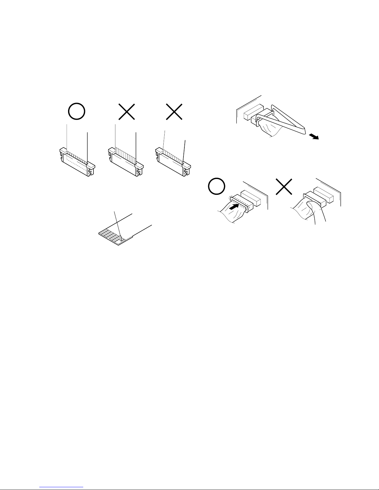
1-1. NOTE FOR REPAIR
Make sure that the flat cable and flexible board are not cracked of
bent at the terminal.
Do not insert the cable insufficiently nor crookedly.
Cut and remove the part of gilt
which comes off at the point.
(Be careful or some
pieces of gilt may be left inside)
When remove a connector, don’t pull at wire of connector.
It is possible that a wire is snapped.
When installing a connector, don’t press down at wire of connector.
It is possible that a wire is snapped.
1-2. POWER SUPPLY DURING REPAIRS
In this unit, about 10 seconds after power is supplied to the battery terminal using the regulated power supply (8.4V), the po wer is shut of f so
that the unit cannot operate.
The following method is available to prevent this.
Method 1.
Use the AC power adaptor (AC-L10, AC-VQ800 etc.).
1-2
DCR-TRV360/TRV361/TRV460/TRV460E/TRV461E
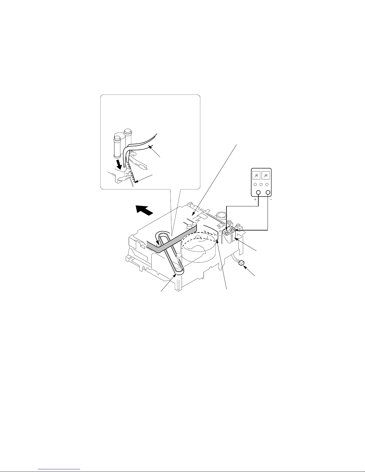
1-3. TO TAKE OUT A CASSETTE WHEN NOT EJECT (FORCE EJECT)
1 Refer to “SECTION 2 DISASSEMBLY” to remove the mechanism deck block.
2 Disconnect CN2401 (2P) of VC-345 board.
3 Add +5V from the DC POWER SUPPLY and unload with a pressing the cassette compartment.
4 Pull the timing belt in the direction of
arrow A with a pincette while pressing
the cassette compartment (take care
not to damage) to adjust the bending
of a tape.
5 Let go your hold the cassette
compartment and rise the cassette
compartment to take out a cassette.
Pincette
Timing belt
Timing belt
Press the cassette compartment not to
rise the cassette compartment
[DC power supply]
(+5V)
Adjust the bending of a tape
Disconnect CN2401
of VC-345 board.
Loading motor
A
A
1-3
DCR-TRV360/TRV361/TRV460/TRV460E/TRV461E
1-4. SELF-DIAGNOSIS FUNCTION
1-4-1. Self-diagnosis Function
When problems occur while the unit is operating, the self-diagnosis
function starts working, and displays on the viewfinder or LCD what
to do. This function consists of two display; self-diagnosis display
and service mode display.
Details of the self-diagnosis functions are provided in the Instruction
manual.
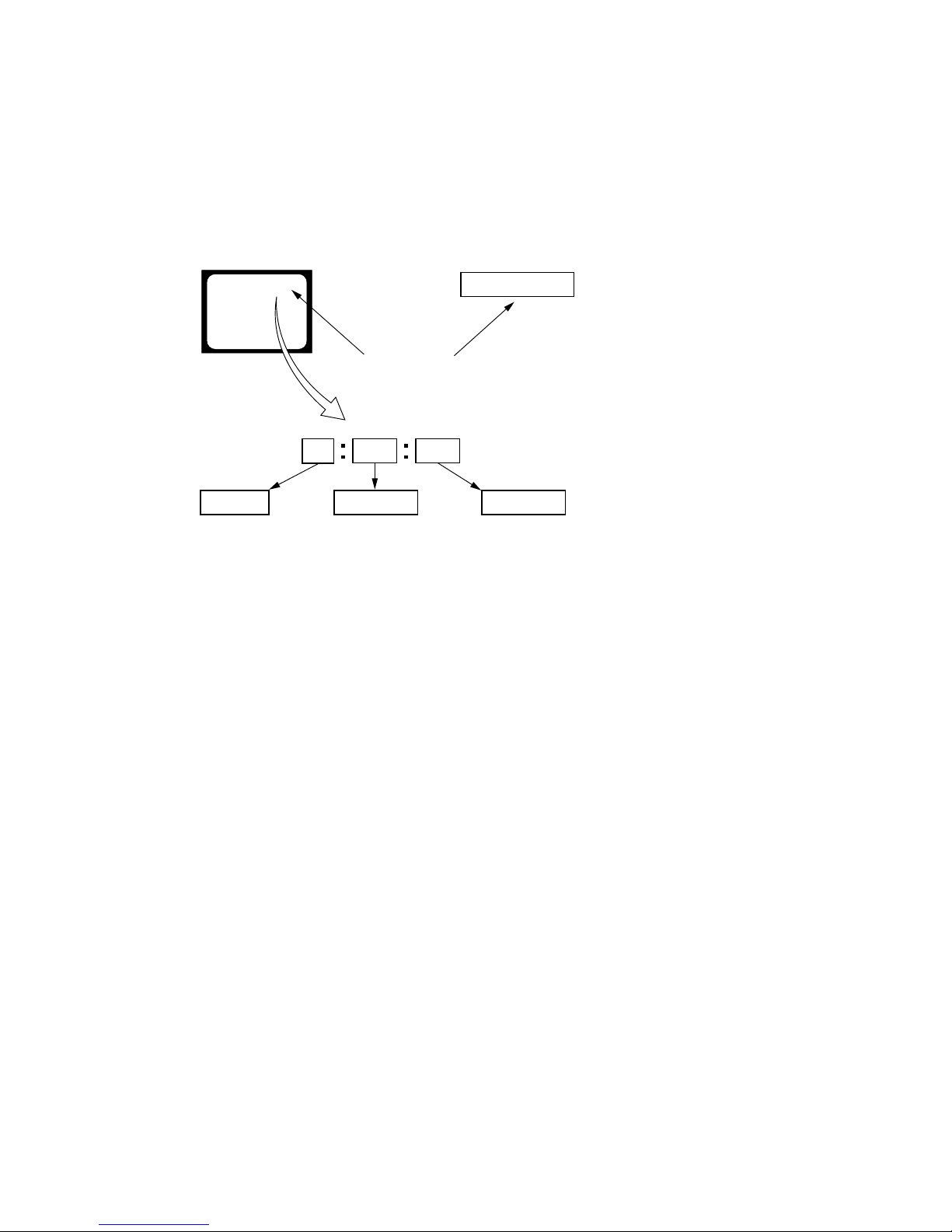
1-4-2. Self-diagnosis Display
When problems occur while the unit is operating, the counter of the
viewfinder or LCD shows a 4-digit display consisting of an alphabet
and numbers, which blinks at 3.2 Hz. This 5-character display
indicates the “repaired by:”, “block” in which the problem occurred,
and “detailed code” of the problem.
1 1
3 1
C : 3 1 : 11
C
Repaired by:
Refer to 1-4-3. Self-diagnosis Code Table .
Indicates the appropriate
step to be taken.
E.g.
31 ....Reload the tape.
32 ....Turn on power again.
Block
Detailed Code
Blinks at 3.2Hz
C : Corrected by customer
H : Corrected by dealer
E : Corrected by service
engineer
Viewfinder Display window
C : 3 1 : 1 1

1-4
DCR-TRV360/TRV361/TRV460/TRV460E/TRV461E
1-4-3. Self-diagnosis Code Table
C
C
C
C
C
C
C
C
C
C
C
C
C
C
C
C
C
C
C
C
C
C
C
C
C
C
C
C
C
Block
Function
04
21
22
31
31
31
31
31
31
31
31
31
31
31
31
31
32
32
32
32
32
32
32
32
32
32
32
32
32
Detailed
Code
00
00
00
10
11
20
21
22
23
30
31
40
41
42
43
44
10
11
20
21
22
23
30
31
40
41
42
43
44
Symptom/State
Non-standard battery is used.
Condensation.
Video head is dirty.
LOAD direction. Loading does not
complete within specified time
UNLOAD direction. Loading does not
complete within specified time
T reel side tape slacking when unloading
.
S reel
side tape slacking when unloading
.
T reel fault.
S reel fault.
FG fault when starting capstan.
FG fault during normal capstan operations.
FG fault when starting drum.
PG fault when starting drum.
FG fault during normal drum operations.
PG fault during normal drum operations.
Phase fault during normal drum operations.
LOAD direction loading motor time-
out.
UNLOAD direction loading motor
time-out.
T reel side tape slacking when
unloading.
S reel side tape slacking when
unloading.
T reel fault.
S reel fault.
FG fault when starting capstan.
FG fault during normal capstan
operations.
FG fault when starting drum.
PG fault when starting drum.
FG fault during normal drum
operations.
PG fault during normal drum
operations.
Phase fault during normal drum
operations.
Self-diagnosis Code
Repaired by:
Correction
Use the InfoLITHIUM battery.
Remove the cassette, and insert it again after one hour.
Clean with the optional cleaning cassette.
Load the tape again, and perform operations from the beginning.
Load the tape again, and perform operations from the beginning.
Load the tape again, and perform operations from the beginning.
Load the tape again, and perform operations from the beginning.
Load the tape again, and perform operations from the beginning.
Load the tape again, and perform operations from the beginning.
Load the tape again, and perform operations from the beginning.
Load the tape again, and perform operations from the beginning.
Load the tape again, and perform operations from the beginning.
Load the tape again, and perform operations from the beginning.
Load the tape again, and perform operations from the beginning.
Load the tape again, and perform operations from the beginning.
Load the tape again, and perform operations from the beginning.
Remove the battery or power cable, connect, and perform
operations from the beginning.
Remove the battery or power cable, connect, and perform
operations from the beginning.
Remove the battery or power cable, connect, and perform
operations from the beginning.
Remove the battery or power cable, connect, and perform
operations from the beginning.
Remove the battery or power cable, connect, and perform
operations from the beginning.
Remove the battery or power cable, connect, and perform
operations from the beginning.
Remove the battery or power cable, connect, and perform
operations from the beginning.
Remove the battery or power cable, connect, and perform
operations from the beginning.
Remove the battery or power cable, connect, and perform
operations from the beginning.
Remove the battery or power cable, connect, and perform
operations from the beginning.
Remove the battery or power cable, connect, and perform
operations from the beginning.
Remove the battery or power cable, connect, and perform
operations from the beginning.
Remove the battery or power cable, connect, and perform
operations from the beginning.

1-5
DCR-TRV360/TRV361/TRV460/TRV460E/TRV461E
E
E
E
E
Block
Function
61
61
62
62
Detailed
Code
00
10
00
01
Symptom/State
Difficult to adjust focus
(Cannot initialize focus.)
Zoom operations fault
(Cannot initialize zoom lens.)
Steadyshot function does not work well.
(With pitch angular velocity sensor output
stopped.)
Steadyshot function does not work well.
(With yaw angular velocity sensor output
stopped.)
Self-diagnosis Code
Repaired by:
Correction
Inspect the lens block focus reset sensor (Pin qs of CN1551 of
VC-345 board) when focusing is performed when the control dial
is rotated in the focus manual mode and the focus motor drive circuit
(IC1554 of VC-345 board) when the focusing is not performed.
Inspect the lens block zoom reset sensor (Pin qg of CN1551 of
VC-345 board) when zooming is performed when the zoom switch
is operated and the zoom motor drive circuit (IC1554 of VC345board) when zooming is not performed.
Inspect pitch angular velocity sensor (SE752 of SI-041 board)
peripheral circuits.
Inspect yaw angular velocity sensor (SE751 of SI-041 board)
peripheral circuits.

DCR-TRV360/TRV361/TRV460/TRV460E/TRV461E
“1-5. CHANGE OF IC4501” is not shown.
Pages 1-6 is not shown.
DCR-TRV360/TRV361/TRV460/TRV460E/TRV461E
2-1 2-2
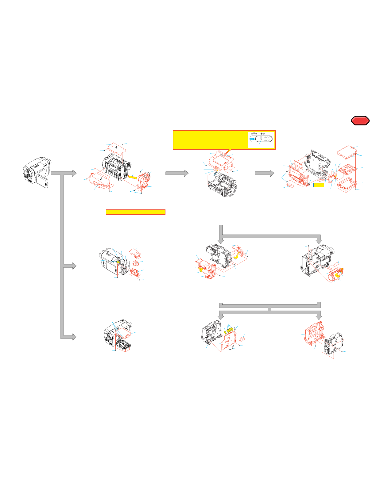
2-1. FLOW CHART
The following flow chart shows the disassembly procedure.
SECTION 2
DISASSEMBLY
HELP
HELP
HELP
NS knob
Note: When you remove Cabinet (R) Block,
or when you assembly, please slide
NS knob to the position of "ON".
Note: Flexible board is connected.
1 Lock ace
x3
2 Cabi (upper)
3 Grip belt
4 Lock ace
x3
5 Cabi (L)
1 Lock ace
x6
2 NS knob to the position of "ON".
3 Cabi (R)
4 VC-345: CN1007
5 VC-345: CN1003
6 VC-345: CN1008
1 Tripod Screw
2 Tapping P2
x2
3 Tapping P2
x6
4 Claw
5 CF-5100
6 Tapping P2
x4
7 Claw
x2
8 P Cabi (C)
9 Tapping P2
x2
q; Tapping P2
x1
qa P Cabi (M)
qs PD-205: CN6005
qd PD-205: CN6001
qf PD-205, LCD901, ND901
qg Tapping P2
x4
qh Hinge assy
6 Lock ace
x3
7 Claw
8 Front panel
9 FP-796: CN754, CN1001
1 Lift up the EVF.
2 Tapping P2
x4
3 Down the EVF.
4 EVF block
5 EVF Cabi (upper)
6 EVF Cabi (lower)
7 FP-797: LCD902
8 EVF lens
1 Tapping P2
x4
2 Claw
x2
3 P Cabi (C)
1 VC-345: CN1013
2 VC-345: CN1016
3 VC-345: CN4001
4 Lock ace
x3
5 EVF/Battely panel block
6 VC-345: CN1009
7 Tapping P2
x1
8 Lock ace
x1
9 SS-5100
1 VF blind sheet
2 VC-345: CN2403, CN2404, CN3201
3 VC-345: CN2401
4 Screw (M1.7)
x2
5 Claw
6 Open the VC-345.
7 VC-345: CN2402
8 VC-345
1 Screw (M1.7)
x3
2 CS frame
1 VC-345: CN1501
2 VC-345: CN1551
3 Lens sheet
4 Lock ace
x2
5 Boss
6 Lens LSV-820A
1
5
2
1
3
4
4
6
6
7
9
8
1
1
2
4
5
6
3
qd
qg
2
3
4
6
7
9
q;
qs
1
5
4
4
7
8
1
3
2
2
3
4
5
6
7
8
1
1
1
2
5
6
9
4
1
2
3
5
6
8
qa
qf
qh
1
2
2
3
4
7
5
6
2
1
3
8

DCR-TRV360/TRV361/TRV460/TRV460E/TRV461E
A
B
Adjustment remote
commander (RM-95)
Info lithium battery
(L series)
I/F unit for LANC control
(J-6082-521-A)
CPC jig connector
(J-6082-539-A)
Cabinet R block
EVF block/
Battery panel block assembly
Mechanism deck
Control key block
(SS-5100)
VC-345 board
Front panel block
Lens block
Press the cassette compartment
in the direction of the arrow A
to move it up in the direction of
the arrow B.
How to move up the cassette
compartment manually
Contacting
surface
Eject switch
When exiting the "Forced Power ON" mode, connect the control
key block (SS-5100) to the CN1009 of VC-345 board. Or, when
ejecting the cassette, connect the control key block (SS-5100) to
the CN1009 of VC-345 board. and press the Eject switch.
Connection to Check the Mechanism deck
To check the mechanism deck, set the Camera or VTR to the "Forced power ON" mode. (Or, connect the control key
block (SS-5100) to the CN1009 of VC-345 board and set the power switch to the "CAMERA" or "PLAY/edit" position.)
Operate the Camera functions of the zoom and focus, the VTR function using the adjustment remote commander
(with the HOLD switch set in the OFF position).
Setting the "Forced Camera Power ON" mode
1) Select page: 0, address: 01, and set data: 01.
2) Select page: A, address: 10, set data: 02 and
press the PAUSE button of the adjustment remote
commander.
Setting the "Forced VTR Power ON" mode
1) Select page: 0, address: 01, and set data: 01.
2) Select page: A, address: 10, set data: 02 and
press the PAUSE button of the adjustment remote
commander.
Exiting the "Forced Power ON" mode
1) Select page: 0, address: 01, and set data: 01.
2) Select page: A, address: 10, data: 00, and press the PAUSE
button of the adjustment remote commander.
3) Select page: 0, address: 01, and set data: 00.
AC adaptor
AC IN
1
5
2
1
3
4
4
6
6
7
9
8
1
1
2
4
5
6
3
4
4
7
8
1
3
2
2
3
4
5
6
7
8
1
1
1
2
5
6
9
4
1
2
3
5
6
2-3 2-4
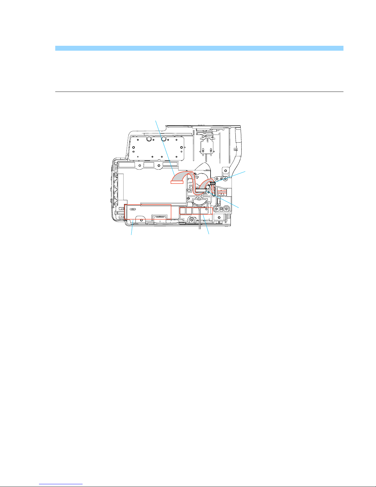
2-2. MECHANISM DECK SERVICE POSITION
2-5
DCR-TRV360/TRV361/TRV460/TRV460E/TRV461E
2-3. LCD SERVICE POSITION
AC adaptor
AC IN
AC adaptor
I/F unit for LANC control
(J-6082-521-A)
CPC jig connector
(J-6082-539-A)
CPC jig connector
L serices Info
LITHIUM battery (7.2Vdc)
LCD panel
PD-205 board
Back light unit
Adjustment
remote commander (RM-95)
Conductor side
CN1011
1
16
LANC jack
AC IN
2
1
3
2-6
DCR-TRV360/TRV361/TRV460/TRV460E/TRV461E
2-4. CIRCUIT BOARDS LOCATION
Board Name Function
CD-472 CCD IMAGER
VC-345 A/D CONVERTER, TIMING GENERATOR, VIDEO/AUDIO DSP,
LENS CONTROL, LENS DRIVE, Hi8/Std8 VTR PROCESS, VIDEO IN/OUT ,
DV SIGNAL PROCESS, REC/PB AMP, DV INTERFACE, STEADYSHOT,
Hi8/Std8 PB AMP, USB/MODE CONTROL, MS INTERFACE, MEMORY,
HI CONTROL, CAMERA/MECHA CONTROL, SERVO, AUDIO, DC CONTROL,
CONNECTOR
PD-205 LCD DRIVE, BACKLIGHT DRIVE
SI-041 STEADYSHOT, JACK
SI-041
VC-345
CD-472
PD-205
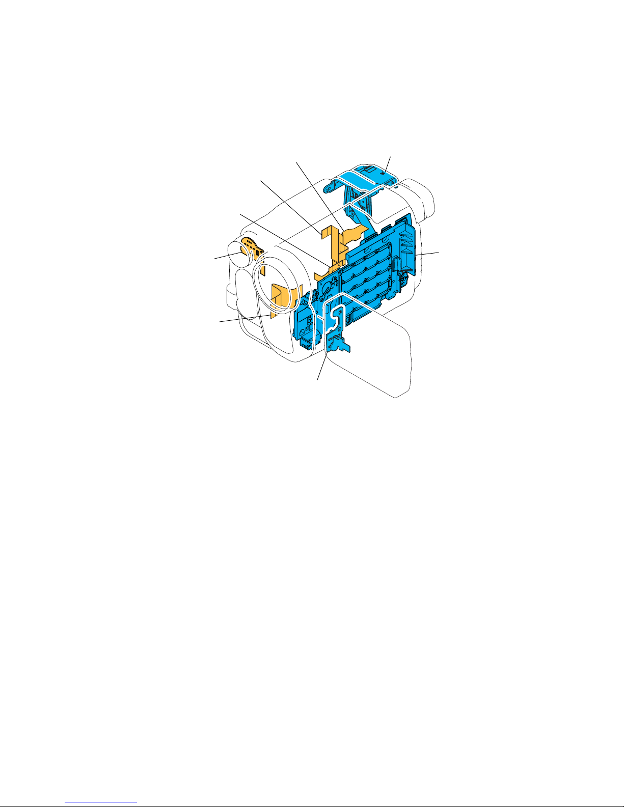
2-7E
DCR-TRV360/TRV361/TRV460/TRV460E/TRV461E
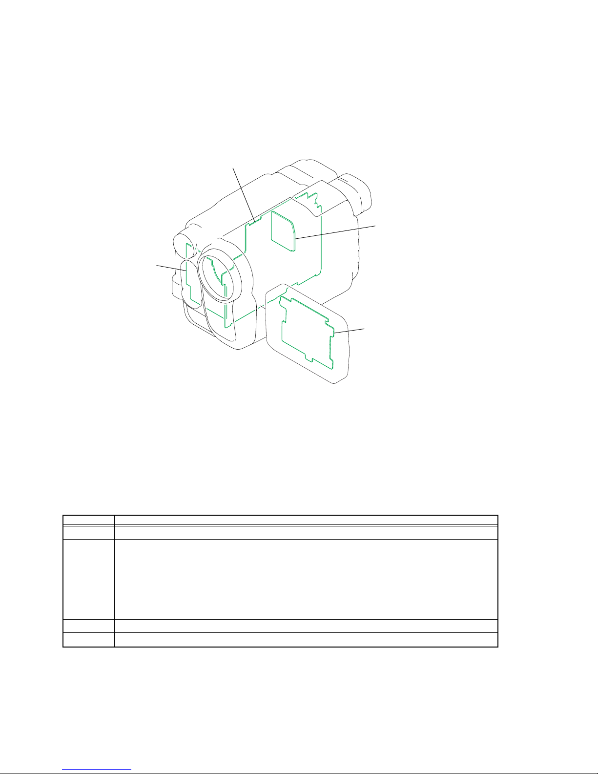
2-5. FLEXIBLE BOARDS LOCATION
FP-792
FP-799
FP-796
CF-5100
PR-5100
SS-5100
FP-797
FFC-005
HELP
DCR-TRV360/TRV361/TRV460/TRV460E/TRV461E
HELP
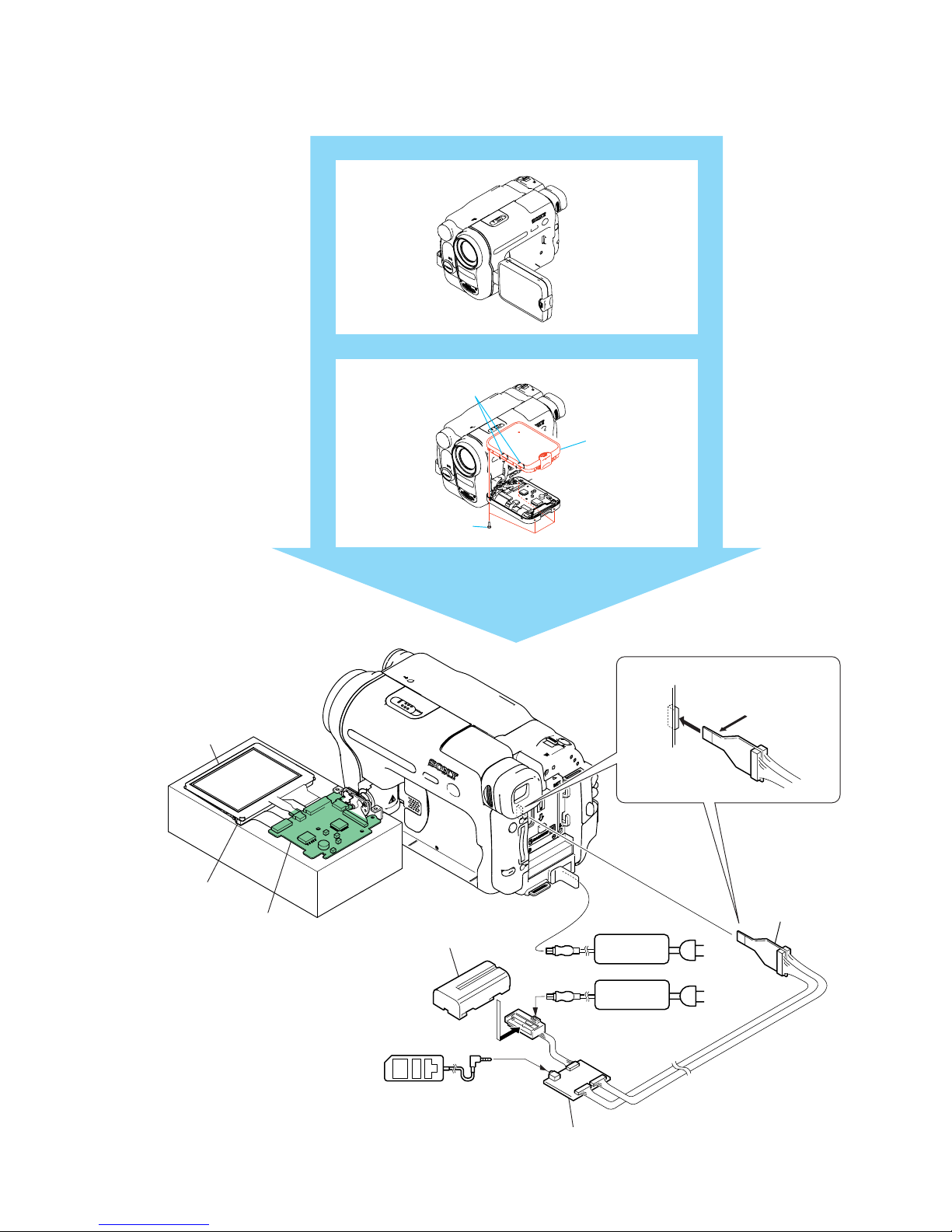
Sheet attachment positions and procedures of processing the flexible boards/harnesses are shown.
Note: Close the LCD panel, when you work.
Claw
Insulating sheet (CF)
Tape (CF)
(TRV360/TRV460/TRV460:E/TRV461E)
Claw
Harness (PD-124)
DCR-TRV360/TRV361/TRV460/TRV460E/TRV461E
Link
Link
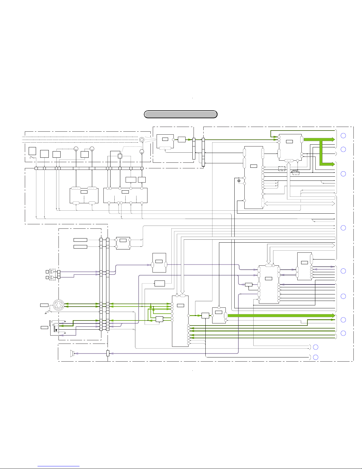
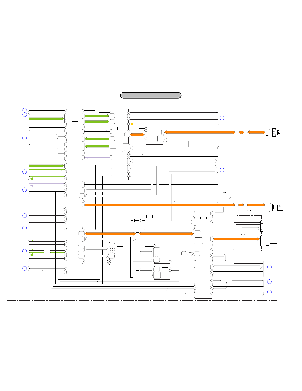
3. BLOCK DIAGRAMS
POWER BLOCK DIAGRAM (2/3)
OVERALL BLOCK DIAGRAM (2/6)
OVERALL BLOCK DIAGRAM (4/6)
OVERALL BLOCK DIAGRAM (3/6)
POWER BLOCK DIAGRAM (1/3)
OVERALL BLOCK DIAGRAM (6/6)
OVERALL BLOCK DIAGRAM (1/6)
OVERALL BLOCK DIAGRAM (5/6)
POWER BLOCK DIAGRAM (3/3)
POWER BLOCK DIAGRAM (2/3)
POWER BLOCK DIAGRAM (3/3)
OVERALL BLOCK DIAGRAM (2/6)
OVERALL BLOCK DIAGRAM (4/6)
OVERALL BLOCK DIAGRAM (5/6)
OVERALL BLOCK DIAGRAM (3/6)
POWER BLOCK DIAGRAM (1/3)
OVERALL BLOCK DIAGRAM (6/6)
OVERALL BLOCK DIAGRAM (1/6)
DCR-TRV360/TRV361/TRV460/TRV460E/TRV461E
3. BLOCK DIAGRAMS
3. BLOCK DIAGRAMS
Hi8/Std8
Hi8/Std8
Hi8/Std8
Hi8/Std8, LINE
Hi8/Std8, LINE
Hi8/Std8
Hi8/Std8
ZOOM MOTOR
IR SWITCH
TEMPLENS TEMP AD
XNS SW
ZM SENS OUT
FOCUS MOTOR
IRIS
METER
12
10
14
8
13 – 16
5 7 17 19 2 4 21 23
(1/18)
FOCUS
MOTOR
DRIVE
IRIS
DRIVE
ZOOM
MOTOR
DRIVE
EN1, DIR1A,
DIR1B
HALL
GAIN
7
1 – 4 12 – 14
CCD
IMAGER
BUFFER
12
4
30
16
5
47
1
2
16
15
44
45
35
37
ı
39
TIMING
GENERATOR
46 4847
23
49
51
20 – 22
AUDIO
PROCESS
(16/18)
46
36
7
39
48
42
14
18
22
L
CN753
CN754 (1/4)
LIA 1
LIA 2
INT MIC L
INT MIC R
INT MIC L,R
XCS AU1
IC 8001 C OUT
34
IC 8001 Y OUT
ADCK27
IC 3701 C OUT
IC 3701
Y OUT
PB IN L, R
REC OUT L, R
SE751
SE752
SP+,–
SP+, –
TG HD, TG VD
CN1001
(1/4)
CN1008
HALL AD, LENS DET,
LENS TEMP AD, XNS SW
PITCH AD, YAW AD
YAW AD
PITCH AD
EN0,EN1, DIR0A,B, DIR1A,B,
FC RST, ZM RST
5 15 12 21 19
IRIS
10 – 7
FC SENS OUT
ZM RST
FC RST
EN0, DIR0A,
DIR0B
HALL
GAIN
IRIS PWM
ZOOM A,B,XA,XB
FOCUS A,B,XA,XB
IRIS HALL(–)
IRIS
DRIVE(–)
CN1551
LENS BLOCK
CN951 CN1501
CLPDM, PBLK,
XSHP, XSHD
CCD OUT
V1 – V4,RG,H1,H2
27 MHz
X1501
VCK
9
ADCK
VCK
ADCK
OVERALL (4/6)
(PAGE 3-7)
Q951
IRIS
DRIVE
Q1551
HALL GAIN
CONTROL
Q1554
SP901
SPEAKER
05
J752
CD-472 BOARD VC-345 BOARD (1/6)
MM MM
MM
IC1554
9 – 12
PITCH SENSOR
YAW SENSOR
SI-041 BOARD (1/4)
33
30
29
4
7
8
A/V
CONTROL KEY BLOCK (CF-5100) (1/2)
24
26
22
19
18
1 – 4
IC951
1
7
ı
9
11
ı
14
14
19
21
ı
23
36
34
2
ı
11
VCK
AV JACK IN, XS JACK IN
ACC-CONT, AGC-CONT, CLPVO
44
5
IC 2201 C OUT
IC 2201 Y OUT
IC 8001 C OUT
CPLVO
IC 8001 Y OUT
IC 2201 C OUT
ACC-CONT
IC 2201 Y OUT
OVERALL (3/6)
(PAGE 3-5)
VIDEO IN/OUT
(6/18)
S/H, AGC,
A/D CONVERTER
(1/18)
18
21
22
STEADYSHOT
(9/18)
8
12218
RG, H1, H2
1
ı
4
25
26
31
28
IRIS PWM
CK CONT
V1 – V4
OVERALL (2/6)
(PAGE 3-3)
S VIDEO
J751
1
2
11
9 10
XVIDEO IN
XCS IC 3701
LINE Y ON
2
5
HALL
AMP
HALL
BIAS
1
20
IRIS
BIAS(–)
H
2322
IRIS BIAS(+)
IRIS HALL(+)
6
HALL
OFFSET
73
HALL
REF
HALL AD
FOCUS
SENSOR
ZOOM
SENSOR
17
LENS
TEMP
SENSOR
(4/18)
FRQ TUNE
20
CLPOB
25
XS JACK IN
AV JACK IN
36
42
48
41
34
ZSG1, ZV1, TG ID
VGAT
ZSG1
ZV1
TG ID
VGAT
3
4
6
OVERALL (2/6)
(PAGE 3-3)
7
OVERALL (3/6)
(PAGE 3-5)
8
OVERALL (2/6)
(PAGE 3-4)
9
OVERALL (2/6)
(PAGE 3-3)
5
A : VIDEO SIGNAL
A : AUDIO SIGNAL
IC1552
(4/18)
IC1501
IC1502
CAM DD ON
4
5
7
8
2
3
15
16
AUDIO
A/D, D/A
CONVERTER
(16/18)
IC5402
DATA TO SFD
IC5401
MIC AMP
(16/18)
IC5801
MUTE
59
2
63
3
64
57
58
A/D
CONVERTER
(3/18)
IC8501
2
19
9
12
HALL OFFSET, HALL GAIN, HALL REF
Q5401, 5402
MUTE
DC LEVEL
DETECTOR
Q3701
VIDEO
BUFFER
Q8504
Q3702, 3703
IC3701
IC2001
1
3
32 5
20
SDC IN
40
43
XRST VTR
XRST VTR
PB C RF
IC 3701 Y OUT
OVERALL (4/6)
(PAGE 3-7)
2
OVERALL (3/6)
(PAGE 3-5)
1
46
14
24
26
OVERALL (2/6)
(PAGE 3-3)
10
BEEP
KASYAON
R
8
12
SFD BCK
DEM 0, 1,
XPWAD, XPWDA
DATA FROM SFD
9
11
SFD FCK
PB RF
AFM FSC
RF SWP
28
AU BPF
29
BPF MONI
1.7M DEV, 1.5M DEV
SFD LRCK
10
S Y I/O
S C I/O
S Y I/O
S C I/O
VIDEO I/O VIDEO I/O
AUDIO L I/O
AV JACK IN
XS JACK IN
AUDIO R I/O
AUDIO L,R I/O
MIC L,R
CH CS, CH SO, CH SCK
CH CS, CH SO, CH SCK
VSP SI, VSP SO, XVSP SCK
VD SO, VD SCK
VD SO, VD SCK
XCS IC 3701
CAM SI, CAM SO, CAM SCK, CAM CS
15
ı
24
AD0 C – AD9 C
17
18
5
1
14
AD0 – AD9
AD0 –AD9
8
ı
6
6
7
13
14
1
47
AGC-CONT
13
11
15
18
19
12
17
NIGHT
SHOT
PLUS
MIC901
MICROPHONE
R1510
R1507
TRV460/TRV460E
/TRV461E
TRV360/TRV361
3-1. OVERALL BLOCK DIAGRAM (1/6)
3-1 3-2
( ) : Number in parenthesis ( ) indicates the division number of schematic diagram where the component is located.
SECTION 3
BLOCK DIAGRAMS
DCR-TRV360/TRV361/TRV460/TRV460E/TRV461E
3. BLOCK DIAGRAMS
3. BLOCK DIAGRAMS
3-3 3-4
3-2. OVERALL BLOCK DIAGRAM (2/6)
( ) : Number in parenthesis ( ) indicates the division number of schematic diagram where the component is located.
A : VIDEO SIGNAL
A : AUDIO SIGNAL
A : VIDEO/AUDIO SIGNAL
A : VIDEO/AUDIO/SERVO SIGNAL
XCS IC8001
TRCKO
LCKO
LCKO
CN1001
(2/4)
CN754
(2/4)
PANEL R
PANEL HD, PANEL VD
05
PANEL B
PANEL G
VC-345 BOARD (2/6)
IC6001
DV SIGNAL
PROCESS
(7/18)
IC5701
USB CONTROL,
MEMORY STICK
INTERFACE,
MODE CONTROL
(11/18)
IC5703
XTAL OSC
(11/18)
EVF G/BW Y
42
ı
45
IC8002
16M
SDRAM
(3/18)
IC8301
DV INTERFACE
(9/18)
6
ı
9
SI-041 BOARD (2/4)
(USB)
92
93
EVF HD, EVF VD
95
96
104 47
79
41
45
139
143
40
46
39
45
21
78 60
TPX, TPY, TP SELE1
ACC-CONT, AGC-CONT,
CLPVO
OVERALL (3/6)
(PAGE 3-5)
16
OVERALL (1/6)
(PAGE 3-2)
9
OVERALL (5/6)
(PAGE 3-10)
19
OVERALL (5/6)
(PAGE 3-9)
18
OVERALL (4/6)
(PAGE 3-7)
17
CN751
DV
27
188
LINEOUT V
LINEOUT V
164
BIRDS VD
VFI OE
USB XEN
162
BIRDS FLD
163
VREF
165
ALIGN VD
161
160
80
1
CN752
36
VCK
VCK
BUFFER
Q8001
XCS IC 8301
XCS IC 8301
158
XCS IC 6001
47
48
224
ı
231
233
234
IC8001
VIDEO/AUDIO DSP,
D/A CONVERTER,
LENS CONTROL
(2/18)
150
ı
152
97
ı
99
237
98
ı
116
252
ı
261
157
SYS V
XCS IC 8001
REC PROOF
SYS V
USB CLK
24
MEMCK OUT
XSYS RST
141
216
ZSG1, ZV1, TG ID
33
IC 3701 C OUT Hi8/Std8, LINE
Hi8/Std8, LINE
245
ADCK27
217
236
ZSG1
ZV1
DIR0A,B
EN0,1
TG ID
DIR1A,B
222
VGAT
241
221
CLPOB
OVERALL (1/6)
(PAGE 3-2)
3
OVERALL (1/6)
(PAGE 3-2)
7
OVERALL (1/6)
(PAGE 3-2)
5
OVERALL (4/6)
(PAGE 3-8)
13
OVERALL (5/6)
(PAGE 3-9)
14
OVERALL (6/6)
(PAGE 3-11)
15
OVERALL (1/6)
(PAGE 3-2)
10
OVERALL (3/6)
(PAGE 3-5)
11
SPCK
OVERALL (4/6)
(PAGE 3-7)
12
SPCK
139
20
119 120
162 163
70 71
121 122
54 55 57
107 109 110
152 – 155
189 190 192
13 14
72 73
149 150
186 187
154 156
158 159
123 – 125
166
24 – 26
29 – 32
34 – 37
219
220
CAM DD ON
EN0,1, DIR0A,B, DIR1A,B
TG HD, TG VD
164
165
287
288
237
238
FC RST, ZM RST
127
168
301
302
126
167
298
299
239
248
246
247
250
251
AD0 C – AD9 C
268
ı
271
RYO0 – RYO3
264
ı
267
RYI0 – RYI3
HYO, HCO
ADATAIN0,1
ADATAOUT0,1
RECDT
RECA1,2
RECCK
RF IN
RECDT
RECA1,2
RECCK
RF IN
12
75
284
285
HYI, HCI
272
273
275
276
RCI0 – RCI3
279
ı
282
RCO0 – RCO3
AD0 – AD9
IC 8001 Y OUT
53
IC 8001 C OUT
60
DATA TO SFD
87
DATA FROM SFD
89
SFD BCK
82
SFD LRCK
SFD BCK
15
DSCK VM
DSCK VM
DSCK VM
XCS SDRAM VM
SFD LRCK
62
XSYS RST
83
SFD FCK
85
KASYAON
86
168
169
58
59
111
112
3
114
157
FRRV, TRRV, TRRT
FRRV, TRRV, TRRT, DRP
FRRV, TRRV, TRRT, DRP
SWP
91
Q5701, 5702
MODURATOR
LBUS0-3
TPA, NTPA, TPB, NTPBTPA+, –, TPB+, –
XCS IC 8301
XCS IC 6001
D24A00 – D31A07, DXXA08, DXXA09, ALE, WRX, RDX
28
29
D24A00 – D31A07, ALE, WRX, RDX
VSP SI, VSP SO, XVSP SCK VSP SI, VSP SO, XVSP SCK
VSP SI, VSP SO, XVSP SCK
DSCK VM
119 122
SFD LRCK
124
CAM DD ON
TP X
TP SEL1
TP Y
TP SEL2
131
137
249
138
250
239
USB CLK
X5703
48 MHz
177
SYS V
221
REC PROOF
234
168
256
196
CAM SI, CAM SO. CAM SCK. CAM CS
CAM SI, CAM SO. CAM SCK. CAM CS
121 122
124 – 137
2 3 5 6
8 9 11
12 39 40
42 43 45
46 48 49
19 – 24
27 – 32
198 – 205
207 208
210 – 215
D0 VM – D15 VM D0 VM – D15 VM
MDQ0 T – MDQ15 T
A1 VM – A19 VM
MA0 T – MA10 T, MA12 T
2
3
MEMORY
STICK
5
CN1016
2
4
6
2
5
CN1015
1
6
7
1
ı
4
D+, –
VCC
D755
USB D+
185
186
USB DET
USB D+ PULL UP
XS JACK IN
238
253
230
MELODY
MELODY ENV
274
AV JACK IN
BEEP
XVM MAD
86
XDS RESET
220
OSD V
AV JACK IN, XS JACK IN
80
MS XIN
MS LED ON
MS XIN
FOR JIG
MS XIN
MS LED ON
USB D+, USB D–
DATA BUS
ADDRESS BUS
IC5501
16M
SDRAM
(12/18)
2 3 5 6
8 9 11
12 39 40
42 43 45
46 48 49
19 – 24
27 – 32
D0 VM – D15 VM
IC 5001 RXD0, IC 5001 TXD0, IC 5001 SCK0, IC 5001 CS
XCS EEP,
EEP XRDY,
EEP RXD3,
EEP SCK3.
EEP TXD3
A1 VM – A11 VM, A13 VM
IC5502
32M
FLASH
(12/18)
IC5702
EEPROM
(11/18)
1 – 10 13
16 – 25
48
16 – 18
21 – 24
27 – 35
1 – 4 7 – 12
291 – 298
301 – 304
29 – 36
38 – 45
1 – 3
5 6
235 236
103 – 105
D0 VM – D15 VM
A1 VM – A22 VM
A1 VM – A22 VM
35
287
KEY AD 6
145
KEY AD 5
144
KEY AD 1
140
KEY AD 0
139
18 71
XCS FLASH
XSYS RST
26
12
69
35
MXCSO
190
18
MS DIO, MS BS, MS SCLK
MS DIO, MS BS, MS SCLK
149
USB D+, USB D–
USB D+, USB D–
HI SI, HI SO. XHI SCK. XCS MECHA
HI SI, HI SO. XHI SCK. XCS MECHA
28
29
31
32
35
34
1
9
8
6
5
2
3
USB
PULL UP
USB 3.1V
Q1007
78
81
85
KEY AD 0, 1, 5. 6
MS LED ON
93
ı
96
66
64
62
171 174
176 – 185
TP SELECT SWITCH
Q5703
IR ON
254
D24A00 – D31A07, DXXA08, DXXA09, ALE, WRX, RDX
( ) : Number in parenthesis ( ) indicates the division number of schematic diagram where the component is located.
DCR-TRV360/TRV361/TRV460/TRV460E/TRV461E
3. BLOCK DIAGRAMS
3. BLOCK DIAGRAMS
A : VIDEO SIGNAL
A : AUDIO SIGNAL
A : SERVO SIGNAL
A : VIDEO/SERVO SIGNAL
A : VIDEO/AUDIO/SERVO SIGNAL
Q3202, 3204, 3205
FLYING
VIDEO HEAD
ERASE
CN3201
RF MON
ODD
ODD (SP1)
EVEN (SP2)
05
XFE ON
RF SWP
CN1011 (1/3)
EVEN
SW DIR
PB RF
IC3201
REC/PB AMP
(8/18)
5
2
BPF MONI
3
11
5
4
7
8
9
ERASE HAED
OSC
Q3206 – 3209
Hi8/Std8
PB ON SWITCH
187
ı
196
IC2201
IC3001
Hi8/Std8
VTR PROCESS
(5/18)
30
44
35
25
46
3
4
10
9
38
OVERALL (4/6)
(PAGE 3-8)
21
CPC
(FOR CHECK)
IC1601
EVR
(D/A CONVERTER)
(10/18)
FREQ TUNE
BPF MONI
HALL OFFSET, HALL GAIN, HALL REF
27
28
9
11
15
DA STRB
SPCK
16
RF SWP
RF SWP
4
3
23
20
5
24
22
AU BPF
1.7M DEV, 1.5M DEV
10
REC Y/MT CONT
REC L CONT
RP IR
MT Q
MT FO
OVERALL (1/6)
(PAGE 3-2)
6
OVERALL (2/6)
(PAGE 3-3)
11
37
SW PS
DRUM 8PB
ALL PS
VCK
198
IC 2201 Y OUT
4
IC 2201 C OUT
213
ADCK
185
43
13
XME/MP
SW PS
ALL PS
XME/MP
26
DOC DET
REC Y/MT CONT
RP POWER SAVE
AGC SLOW
REC L CONT
RP IR
DOC DET
MT FO
MT Q
12
21
8
AGC EVR
LPF FO
PB FBDP
6
XMP/ME
34
36
AGC EVR
LPF FO
PB FBDP
22
XMP/ME FE (X)
40
42
95
ı
97
17
ı
19
VD SI, VD SO, VD SCK
53
AFC F0
VCO
Q2207
83
JOG VD
84
X1/2 SWP
85
SWP DIR
87
ATF SAMPLE
88
SYS V
93
94
101
CK CONT
157
XTBC V RST
158
TBC VD
MECHA HD, MECHA VD
OVERALL (4/6)
(PAGE 3-7)
OVERALL (1/6)
(PAGE 3-2)
1
OVERALL (2/6)
(PAGE 3-4)
16
OVERALL (1/6)
(PAGE 3-2)
8
20
49
PB C RF
51
RF AGC OUT
PB C RF
98
XCS IC 2201
99
XRST IC 2201
AFC F0 ADJ
AFC F0 ADJ
PB RF
PB RF
AFM FSC
79
67
AFM FSC
SPCK
81
DOP
77
RECDT
RECA1,2
RECCK
RF IN
RECDT
RECA1,2
RECCK
RF IN
DV PB RF
RF MON
AD0 – AD9
VC-345 BOARD (3/6)
9
18
11
10
14
7
3
48
8
12
46
RP PB MODE
13
Hi8/Std8
PB AMP
(10/18)
CAM SO, CAM SCK
AGC
CONTROL
Q3001
RP POWER SAVE
AGC SLOW
RP PB MODE
RF ENV DET
DOP
Hi8/Std8
Hi8/Std8
Hi8/Std8
Hi8/Std8
66
15
19
RF ENV DET
5
Q3002
BUFFER
TRV460/TRV460E/TRV461E
M2000/M2200
MECHA DECK (1/2)
M2000: TRV460/TRV460E/TRV461E
M2200: TRV360/TRV361
3-5 3-6
3-3. OVERALL BLOCK DIAGRAM (3/6)
( ) : Number in parenthesis ( ) indicates the division number of schematic diagram where the component is located.
 Loading...