

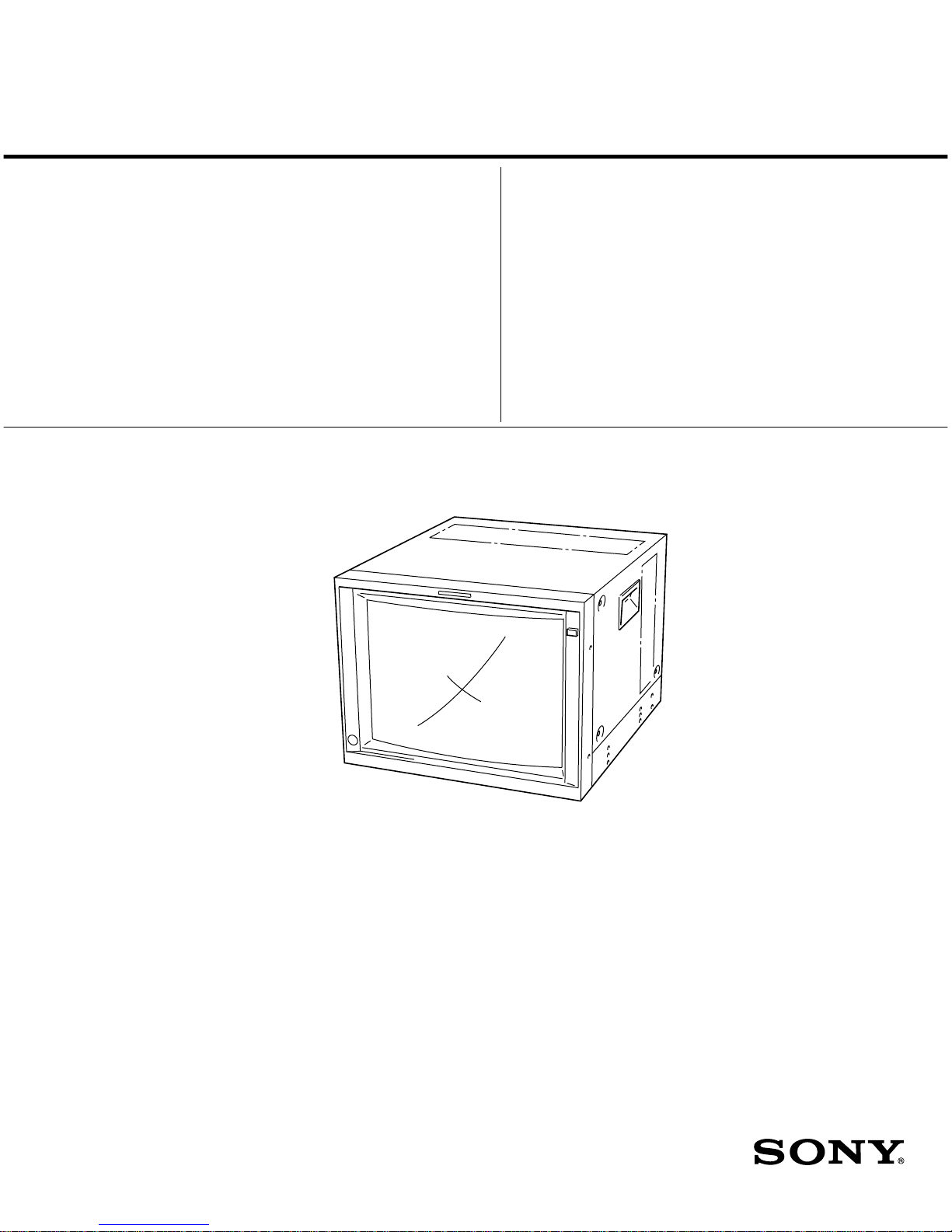
Sony TRINITRON PVM-14L5, TRINITRON PVM-20L5, TRINITRON PVM-D20L5A, TRINITRON PVM-D14L5A Service Manual
.............. ......... ....................
SERVICE MANUAL
.............. ......... ....................
MODEL
DEST. CHASSIS NO. MODEL DEST. CHASSIS NO.
PVM-14L5 US/CND SCC-G61K-A
PVM-20L5 US/CND SCC-G61L-A
PVM-D14L5A AUS SCC-H03D-A
PVM-D20L5A AUS SCC-H03E-A
TRINITRON® COLOR VIDEO MONITOR
REVISED-1

PVM-14L5/20L5/D14L5A/D20L5A
WARNING!!
AN INSULATED TRANSFORMER SHOULD BE USED DURING
ANY SERVICE TO AVOID POSSIBLE SHOCK HAZARD, BECAUSE OF LIVE CHASSIS.
THE CHASSIS OF THIS RECEIVER IS DIRECTLY CONNECTED
TO THE AC POWER LINE.
SAFETY-RELATED COMPONENT WARNING !!
COMPONENTS IDENTIFIED BY A
!!
!!
! MARK ON THE SCHEMA TIC
DIAGRAMS, EXPLODED VIEWS AND IN THE PARTS LIST ARE
CRITICAL TO SAFE OPERATION. REPLACE THESE COMPONENTS WITH SONY PARTS WHOSE P ART NUMBERS APPEAR
AS SHOWN IN THIS MANUAL OR IN SUPPLEMENTS PUBLISHED BY SONY . CIRCUIT ADJUSTMENTS THAT ARE CRITICAL TO SAFE OPERATION ARE IDENTIFIED IN THIS MANU AL.
FOLLOW THESE PROCEDURES WHENEVER CRITICAL COMPONENTS ARE REPLACED OR IMPROPER OPERATION IS
SUSPECTED.
ATTENTION!!
AFIN D’ÉVITER TOUT RISQUE D’ÉLECTROCUTION
PROVENANT D’UN CHÂSSIS SOUS TENSION, UN
TRANSFORMA TEUR D’ISOLEMENT DOIT ETRE UTILISÉ LORS
DE TOUT DÉPANNAGE.
LE CHÂSSIS DE CE RÉCEPTEUR EST DIRECTEMENT
RACCORDÉ Á L’ALIMENTATION SECTEUR.
ATTENTION AUX COMPOSANTS RELATIFS Á LA
SÉCURITÉ!!
LES COMPOSANTS IDENTIFIÉS PAR UNE MAPQUE
!!
!!
! SUR
LES SCHÉMAS DE PRINCIPE, LES VUES EXPLOSÉES ET LES
LISTES DE PIECES SONT D’UNE IMPORTANCE CRITIQUE
POUR LA SÉCURITÉ DU FONCTIONNEMENT. NE LES
REMPLACER QUE PAR DES COMPOSANTS SONY DONT LE
NUMÉRO DE PIÈCE EST INDIQUÉ DANS LE PRÉSENT
MANUEL OU DANS DES SUPPLÉMENTS PUBLIÉS P AR SONY.
LES RÉGLAGES DE CIRCUIT DONT L’IMPORTANCE EST CRITIQUE POUR LA SÉCURITÉ DU FONCTIONNEMENT SONT
IDENTIFIÉS DANS LE PRÉSENT MANUEL. SUIVRE CES
PROCÉDURES LORS DE CHAQUE REMPLACEMENT DE
COMPOSANTS CRITIQUES, OU LORSQU’UN MAUVAIS
FONCTIONNEMENT EST SUSPECTÉ.
! WARNING
This manual is intended for qualified service personnel only.
To reduce the risk of electric shock, fire or injury, do not perform any servicing other than that
contained in the operating instructions unless you are qualified to do so. Refer all servicing to
qualified service personnel.
! WARNUNG
Die Anleitung ist nur für qualifiziertes Fachpersonal bestimmt.
Alle Wartungsarbeiten dürfen nur von qualifiziertem Fachpersonal ausgeführt werden. Um die
Gefahr eines elektrischen Schlages, Feuergefahr und Verletzungen zu vermeiden, sind bei
Wartungsarbeiten strikt die Angaben in der Anleitung zu befolgen. Andere als die angegeben
Wartungsarbeiten dürfen nur von Personen ausgeführt werden, die eine spezielle Befähigung
dazu besitzen.
! AVERTISSEMENT
Ce manual est destiné uniquement aux personnes compétentes en charge de l’entretien. Afin
de réduire les risques de décharge électrique, d’incendie ou de blessure n’effectuer que les
réparations indiquées dans le mode d’emploi à moins d’être qualifié pour en effectuer d’autres.
Pour toute réparation faire appel à une personne compétente uniquement.

1
PVM-14L5/20L5/D14L5A/D20L5A
Table of Contents
1. Service Informations
1-1. Board Layout (14 inch) ...............................................................................1-1
1-2. Disassembly (14 inch).................................................................................1-1
1-2-1. Top Cover Removal (14 inch)....................................................1-1
1-2-2. Bezel Assy Removal (14 inch)...................................................1-2
1-2-3. H1 Board Removal (14 inch) .....................................................1-2
1-2-4. H2 Board Removal (14 inch) .....................................................1-3
1-2-5. J , D1, D2 and D Boards Removal (14 inch) .............................1-3
1-2-6. C Board Removal (14 inch) .......................................................1-4
1-2-7. B Block Assy Removal (14 inch)...............................................1-4
1-2-8. K, T, B1, M and B Boards Removal (14 inch) ..........................1-5
1-2-9. Q Block Assy Removal (14 inch) ..............................................1-5
1-2-10. Removal of Anode Cap .............................................................. 1-6
1-2-11. G Board Removal (14 inch) .......................................................1-6
1-2-12. Picture Tube Removal (14 inch) ................................................1-7
1-2-13. Speaker Removal (14 inch) ........................................................ 1-8
1-2-14. Service Position (14 inch) ..........................................................1-8
1-3. Board Layout (20 inch) ...............................................................................1-9
1-4. Disassembly (20 inch)...............................................................................1-10
1-4-1. Top Cover Removal (20 inch)..................................................1-10
1-4-2. Bezel Assy Removal (20 inch).................................................1-10
1-4-3. HA Board Removal (20 inch) .................................................. 1-11
1-4-4. HB Board Removal (20 inch) ..................................................1-11
1-4-5. J, D1, D2 and D Boards Removal (20 inch) ............................1-12
1-4-6. C Board Removal (20 inch) .....................................................1-12
1-4-8. K, T, B1, M and B Boards Removal (20 inch) ........................1-13
1-4-7. B Block Removal (20 inch)......................................................1-13
1-4-9. Q Block Assy Removal (20 inch) ............................................1-14
1-4-10. Removal of Anode Cap ............................................................ 1-14
1-4-11. G Board Removal (20 inch) .....................................................1-15
1-4-12. Picture Tube Removal (20 inch) ..............................................1-15
1-4-13. Speaker Removal (20 inch) ...................................................... 1-16
1-4-14. Service Position (20 inch) ........................................................1-16
2. Set-up Adjustment
2-1. Equipment Required....................................................................................2-1
2-2. Preparations (1) ...........................................................................................2-1
2-3. Preparation (2). Initialization ...................................................................2-16
2-4. Writing Model Data .................................................................................. 2-17
2-5. Picture Output ........................................................................................... 2-17
2-6. Free-run Frequency Adjustment ...............................................................2-17

2
PVM-14L5/20L5/D14L5A/D20L5A
2-7. Landing Adjustment..................................................................................2-18
2-8. H Blanking Adjustment.............................................................................2-19
2-9. Linearity Adjustment ................................................................................2-20
2-10. Convergence Adjustment (1) .................................................................... 2-21
2-11. Deflection Yoke Neck Rotation Adjustment ............................................ 2-22
2-12. Convergence Adjustment (2) .................................................................... 2-22
2-13. G2 Adjustment ..........................................................................................2-23
2-14. White Balance Adjustment (15k)..............................................................2-23
2-15. White Balance Adjustment (33k)..............................................................2-24
2-16. SUB BRIGHT, SUB CONTRAST Adjustment (15 K) ............................ 2-24
2-17. SUB BRIGHT, SUB CONTRAST Adjustment (33 K) ............................ 2-25
2-18. White Balance Interference Correction Adjustment ................................. 2-25
2-18-1. NTSC Composite Adjustment..................................................2-25
2-18-2. PAL Composite Adjustment .................................................... 2-25
2-18-3. COMPONENT Adjustment ..................................................... 2-25
2-18-4. SDI Adjustment........................................................................2-25
2-18-5. HD and SDI Adjustments.........................................................2-26
2-19. Focus Adjustment......................................................................................2-26
3. Safety Related Adjustment
3-1. High Tension Regulator Confirmation........................................................3-2
3-2. Protection Circuit Confirmation..................................................................3-2
3-2-1. HV Protector Circuit Confirmation............................................3-2
3-2-2. 1K Protector Circuit Confirmation.............................................3-2
4. Electrical Adjustments
4-1. Equipment Required....................................................................................4-1
4-2. B Board Adjustments ..................................................................................4-2
4-2-1. Preparations ................................................................................ 4-2
4-2-2. 15k YPBPR SMPTE (601) Signal Adjustment..........................4-3
4.2-2-1. Black Level Adjustment.............................................................4-3
4-2-2-2. CHROMA Leak Adjustment......................................................4-4
4-2-2-3. MATRIX Adjustment ................................................................ 4-4
4-2-3. 15k YPBPR BETACAM SETUP 0 Signal Adjustment ............4-5
4-2-4. 15k YPBPR BETACAM SETUP 7.5 Signal Adjustment .........4-5
4-2-5. 33 k YPBPR SMPTE (709) Signal Adjustment.........................4-6
4-3. B1 Board Adjustments ................................................................................4-8
4-3-1. Preparation .................................................................................4-8
4-3-2. Y OUT Level Adjustment (BYPASS Mode) ............................. 4-9
4-3-3. Clamp Pulse Width Adjustment (NTSC) ...................................4-9
4-3-4. Burst Gate Pulse Width Adjustment (NTSC) ............................4-9

3
PVM-14L5/20L5/D14L5A/D20L5A
4-3-5. 3.58 f0 Adjustment (NTSC) ....................................................... 4-9
4-3-6. Phase Adjustment (NTSC) .........................................................4-9
4-3-7. Level Adjustment (NTSC) .......................................................4-10
4-3-8. Burst Gate Pulse Width Adjustment (PAL) .............................4-10
4-3-9. 4.43 f0 Adjustment (PAL)........................................................4-10
4-3-10. PAL B-Y PHASE Adjustment .................................................4-10
4-3-11. PAL PHASE Adjustment (Normal) .........................................4-11
4-3-12. Level Adjustment (PAL)..........................................................4-11
4-3-13. Level Adjustment (NTSC 443) ................................................4-11
4-3-14. Clamp Pulse Width Adjustment (SECAM) ............................. 4-12
4-3-15. H. Pulse Width Adjustment (SECAM) ....................................4-12
4-3-16. Level Adjustment (SECAM)....................................................4-12
5. Theory of Operation
5-1. B Board ....................................................................................................... 5-1
5-2. BI Board ......................................................................................................5-3
5-3. C Board ....................................................................................................... 5-4
5-4. Deflection Circuit and High Tension Circuit ..............................................5-5
5-7. Power Supply Circuit ..................................................................................5-7
6. Semiconductors................................................................................. 6-1
7. Spare Parts
7-1. Notes on Repair Parts..................................................................................7-1
7-2. Exploded Views ..........................................................................................7-2
7-3. Electrical Parts List ...................................................................................7-11
8. Block Diagrams
Overall (1/2) ................................................................................................8-1
Overall (2/2) ................................................................................................8-2
Q (1/2), B (1/5), T (1/2), K..........................................................................8-3
B (2/5) ......................................................................................................... 8-4
B (3/5) ......................................................................................................... 8-5
Q (2/2), B (4/5, 5/5), M, T (2/2), H1 (14L)/HA (20L), H2 (14L)/HB (20L) ...
8-6
B1 ................................................................................................................8-7
C, D, D1, D2, DY........................................................................................8-8
G, J .............................................................................................................. 8-9

4
PVM-14L5/20L5/D14L5A/D20L5A
9. Diagrams
9-1. Frame Schematic Diagram .......................................................................... 9-3
Frame...........................................................................................................9-3
9-2. Schematic Diagrams and Printed Wiring Boards........................................9-4
Schematic Diagrams
Q (1/2) .........................................................................................................9-5
Q (2/2) .........................................................................................................9-6
T .................................................................................................................. 9-8
B (1/5) ....................................................................................................... 9-11
B (2/5) ....................................................................................................... 9-12
B (3/5) ....................................................................................................... 9-13
B (4/5) ....................................................................................................... 9-14
B (5/5) ....................................................................................................... 9-15
B1 (1/2) .....................................................................................................9-21
B1 (2/2) .....................................................................................................9-22
M ............................................................................................................... 9-24
H1 .............................................................................................................. 9-25
H2 .............................................................................................................. 9-27
HA .............................................................................................................9-29
HB .............................................................................................................9-30
K ................................................................................................................ 9-31
C ................................................................................................................9-33
X ................................................................................................................ 9-34
J ................................................................................................................. 9-35
D ................................................................................................................ 9-37
D2 .............................................................................................................. 9-37
D1 .............................................................................................................. 9-39
G (1/2) .......................................................................................................9-42
G (2/2) .......................................................................................................9-43
Printed Wiring Boards
Q .................................................................................................................. 9-4
T .................................................................................................................. 9-7
B ................................................................................................................9-16
B1 ..............................................................................................................9-20
M ............................................................................................................... 9-23
H1 .............................................................................................................. 9-23
H2 .............................................................................................................. 9-26
HA .............................................................................................................9-28
HB .............................................................................................................9-28
K ................................................................................................................ 9-31
C ................................................................................................................9-32
X ................................................................................................................ 9-34
J ................................................................................................................. 9-35
D2 .............................................................................................................. 9-35
D ................................................................................................................ 9-36
D1 .............................................................................................................. 9-38
G ................................................................................................................ 9-40
1-1
PVM-14L5/20L5/D14L5A/D20L5A
Section 1
Service Informations
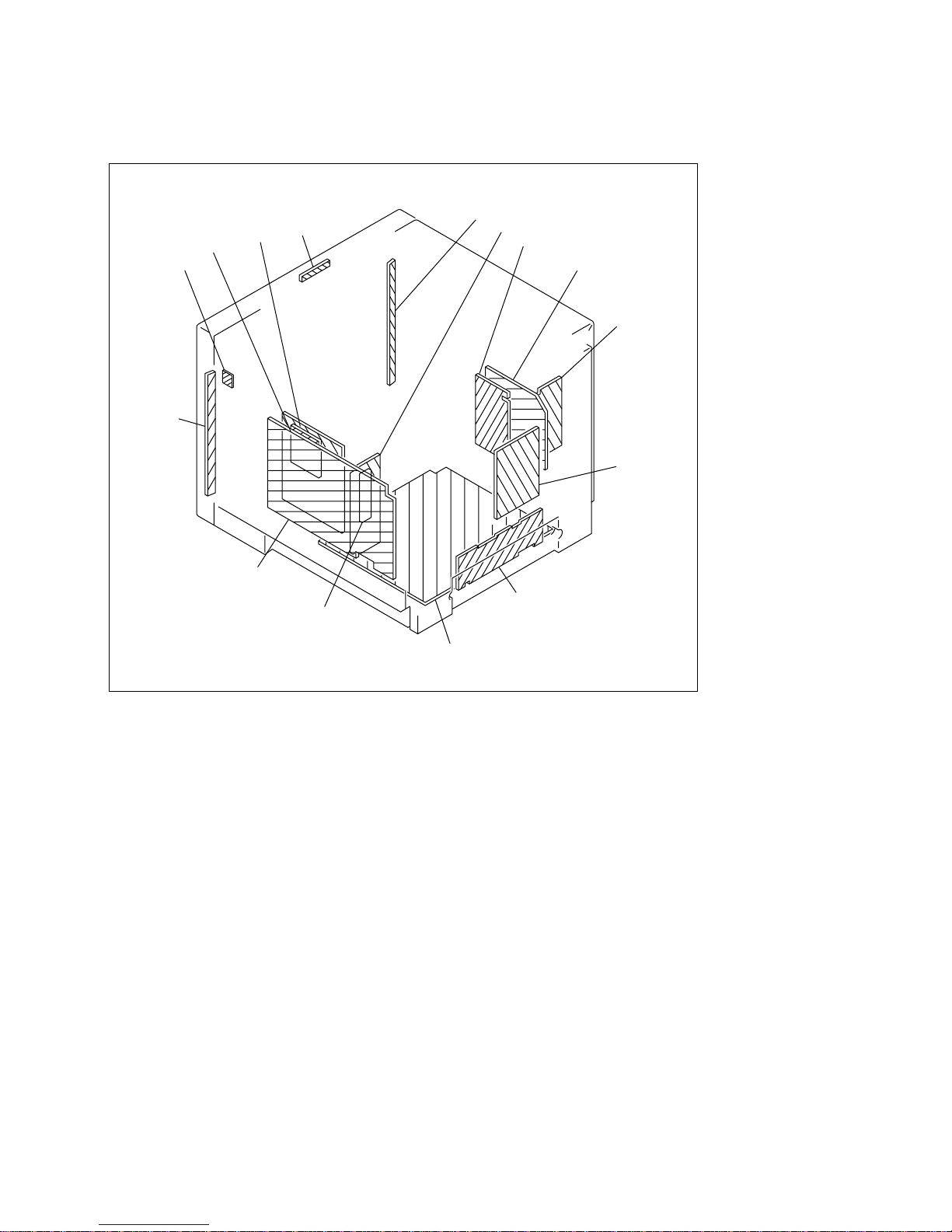
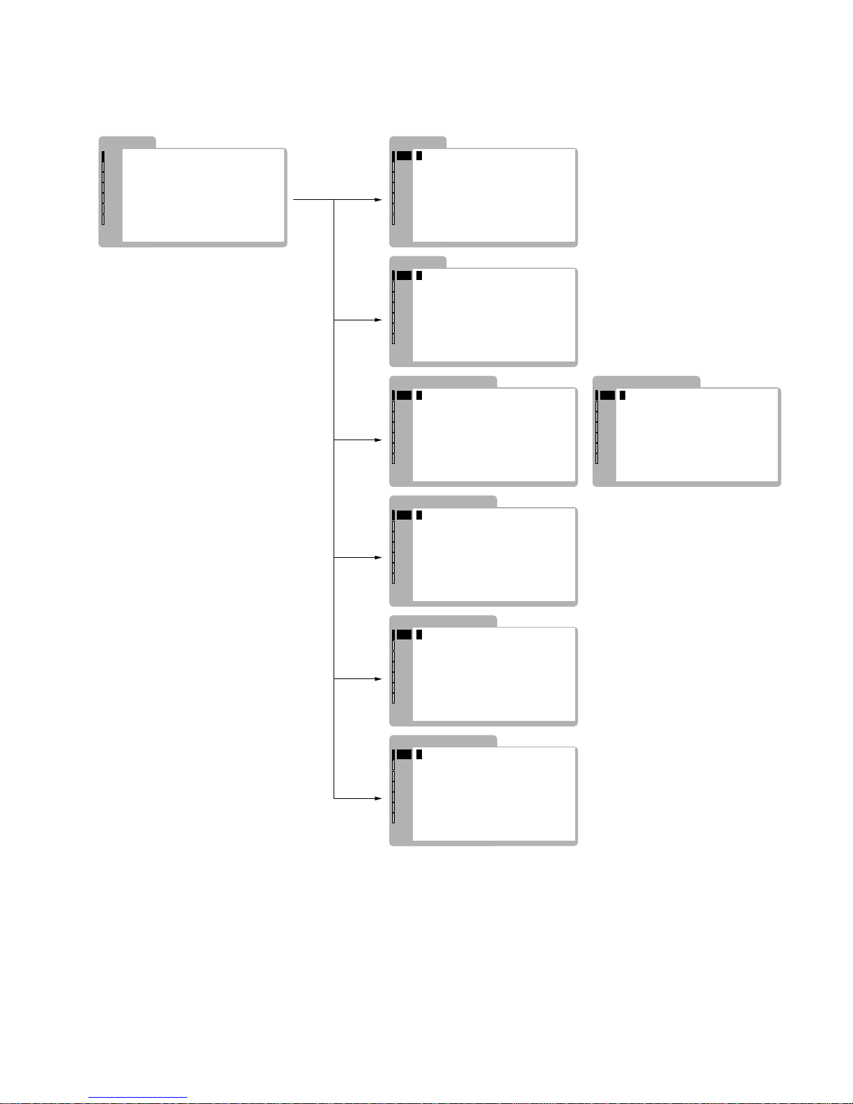
1-1. Board Layout (14 inch)
M
X
D1
B1
B
D
C
Q
G
H1
H2
J
K
D2
T
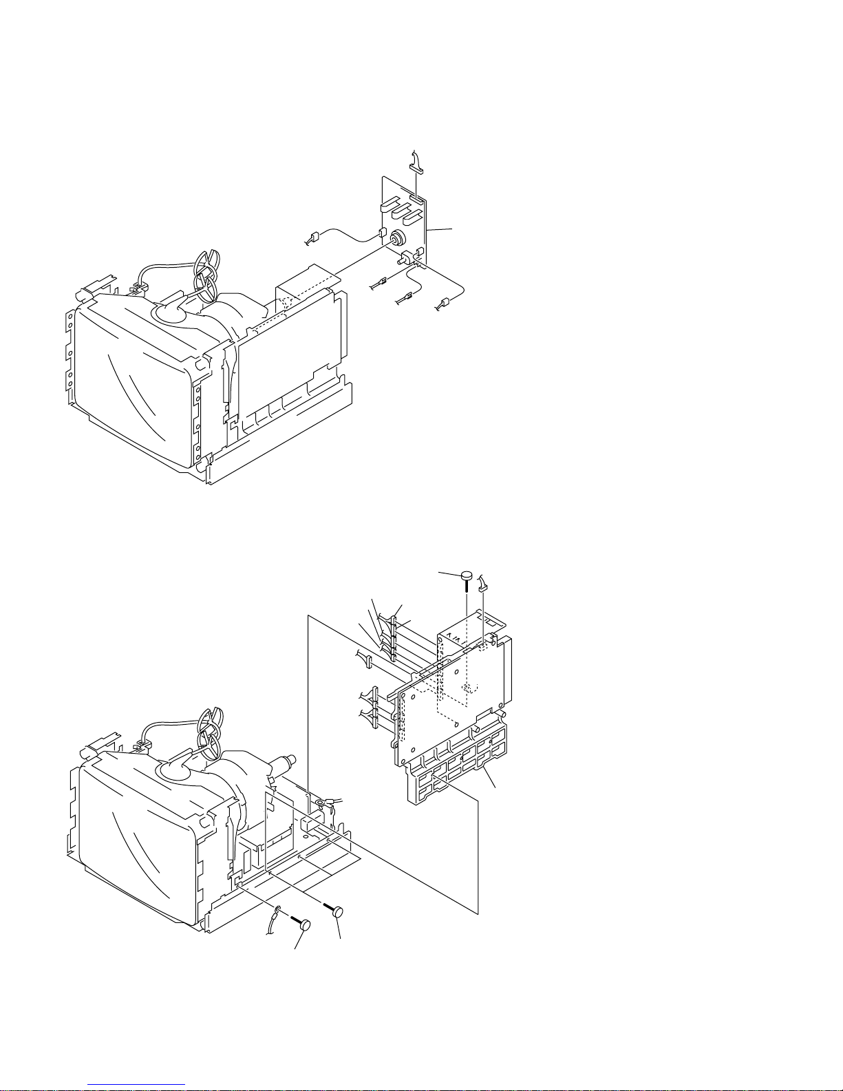
1-2. Disassembly (14 inch)
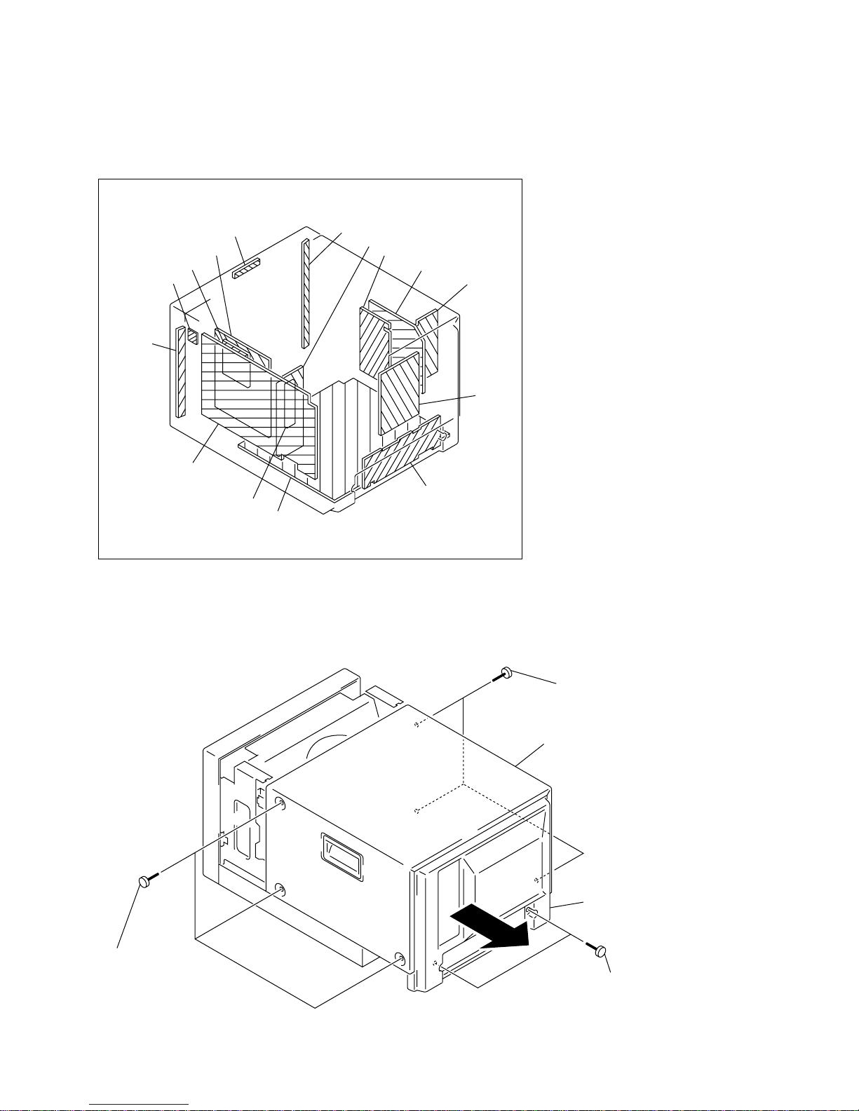
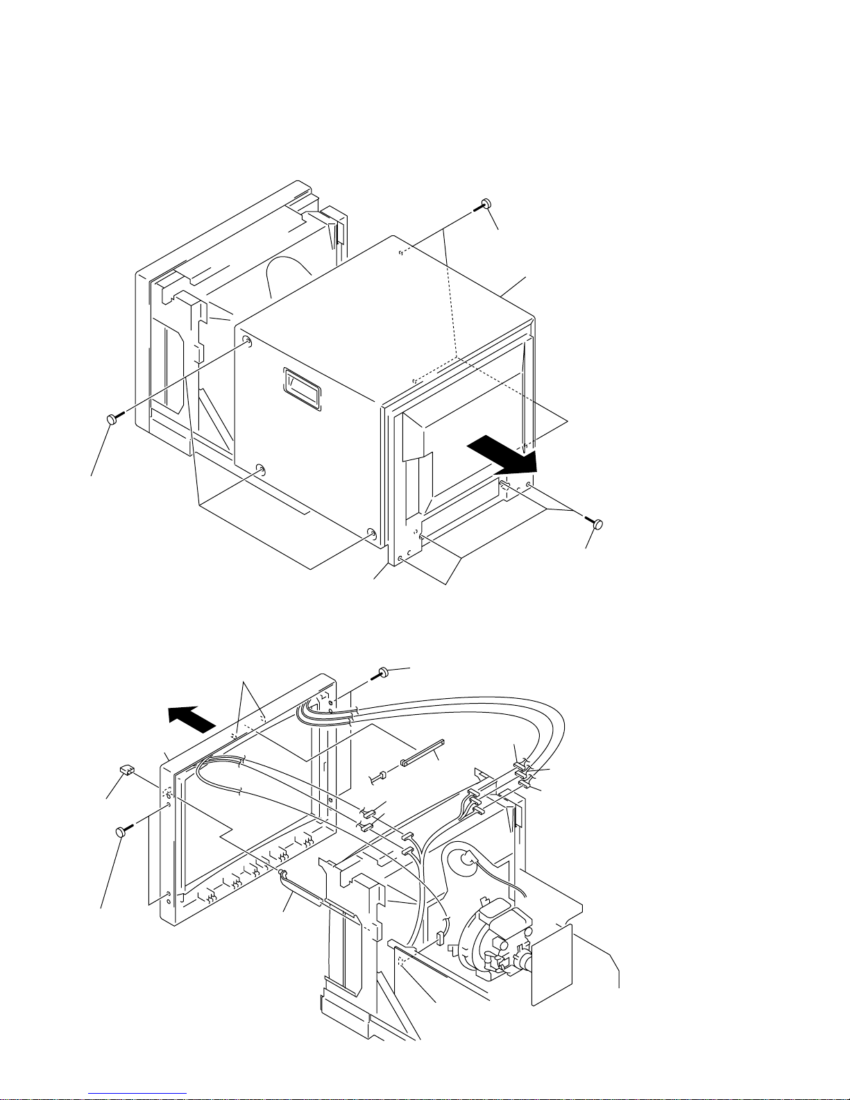
1-2-1. Top Cover Removal (14 inch)
1 Three screws
(claw case screw (OS))
2 Three screws
(claw case screw (OS))
Top cover
Rear cover
4
3 T wo screws
(+BVTT 4 x 8)
1-2
PVM-14L5/20L5/D14L5A/D20L5A
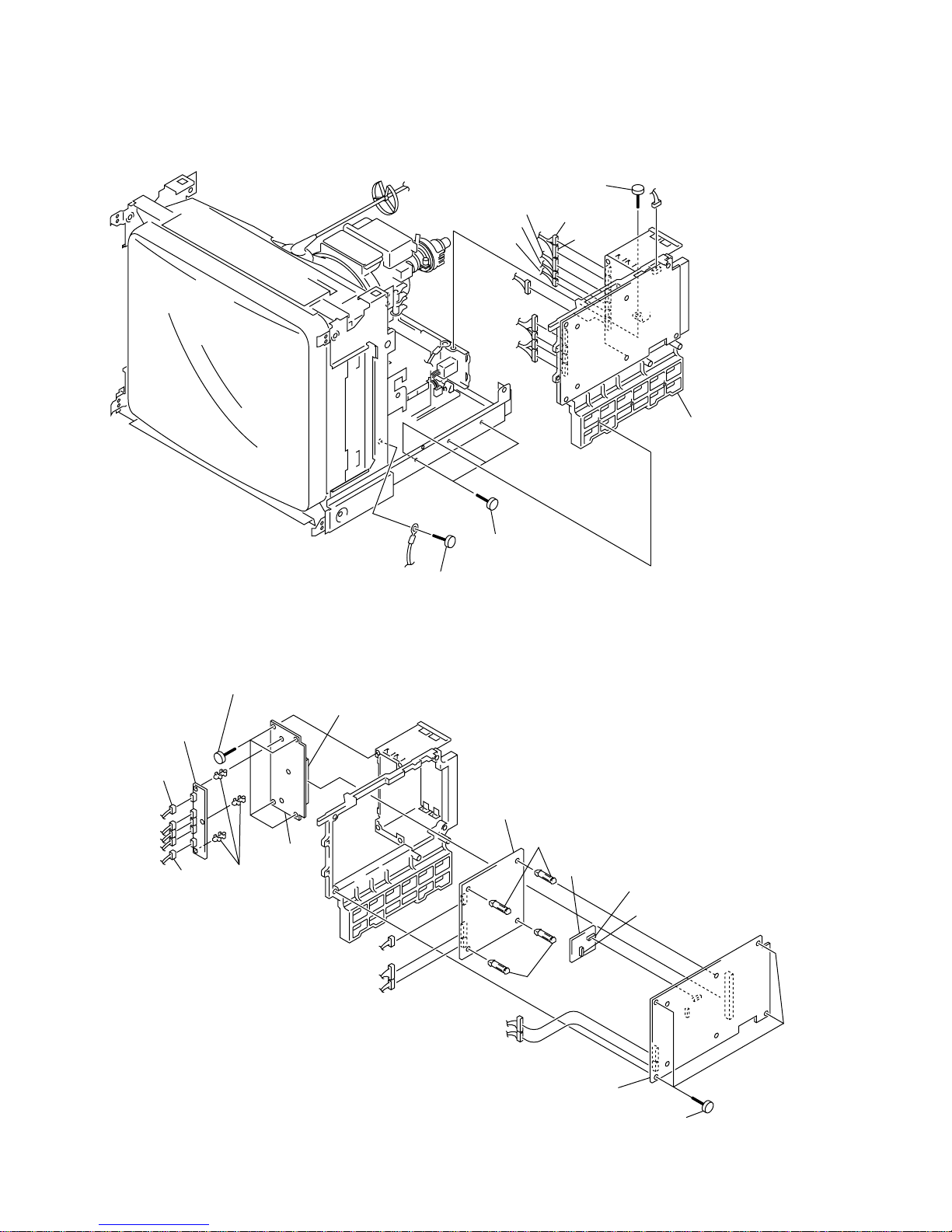
1-2-2. Bezel Assy Removal (14 inch)
3 Two screws (+B 3 x 8)
6 Two claws
5 Shaft switch
4
2 Two screws
(+B 3 x 8)
10 pin
X board
9 pin
7 pin
9 pin
5 pin
CN105
CN900
Bezel assy
1 Power button
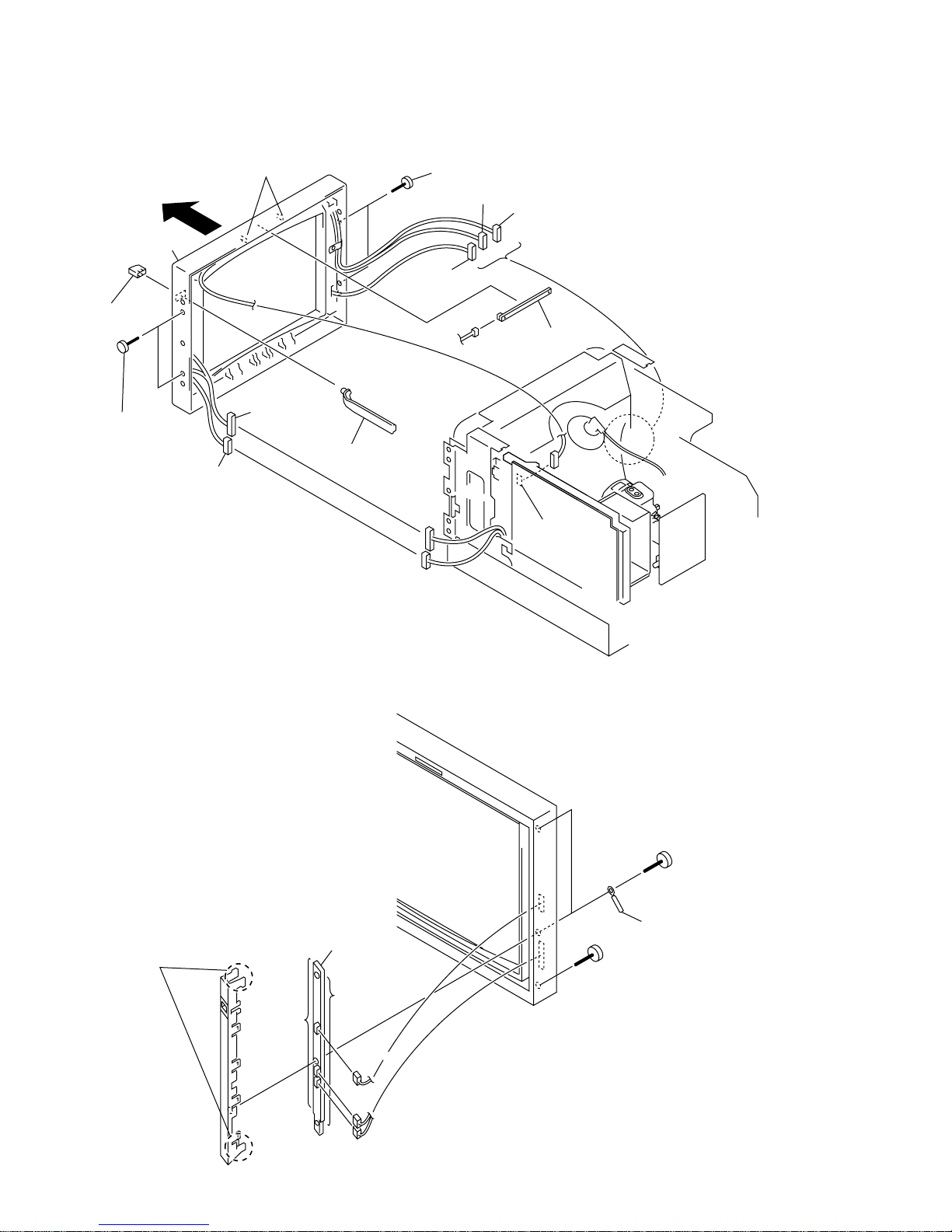
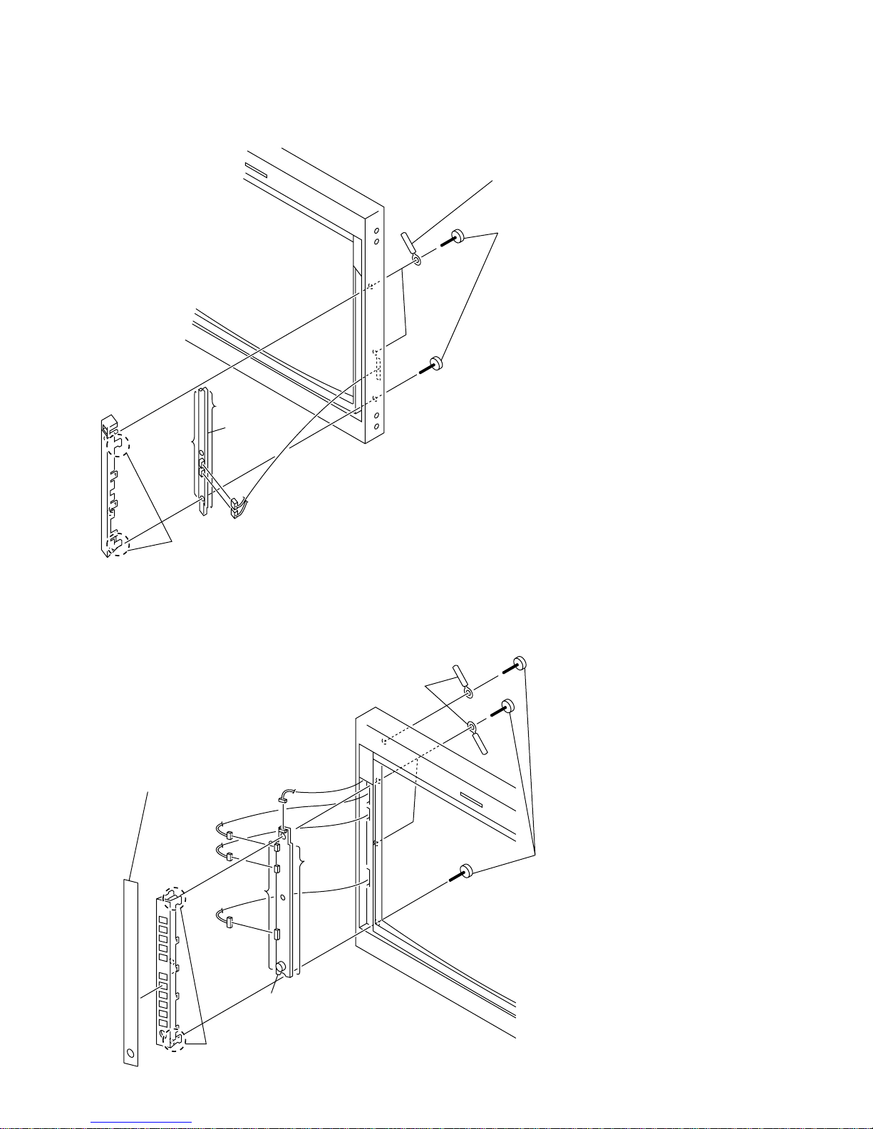
1-2-3. H1 Board Removal (14 inch)
4 Four claws
5 Three
claws
6 Four claws
1 Two screws
(+BVTP 3 x 12)
3 Screw (+BVTP 3 x 12)
2 Two wire holders
CN2903
CN2902
CN2901
H1 board
1-3
PVM-14L5/20L5/D14L5A/D20L5A
1-2-4. H2 Board Removal (14 inch)
3 Four claws
4 Four claws
5 Four
claws
1 Screw (+BVTP 3 x 12)
CN5005
CN5002
CN5001
CN5004
H2 board
2 Wire holder
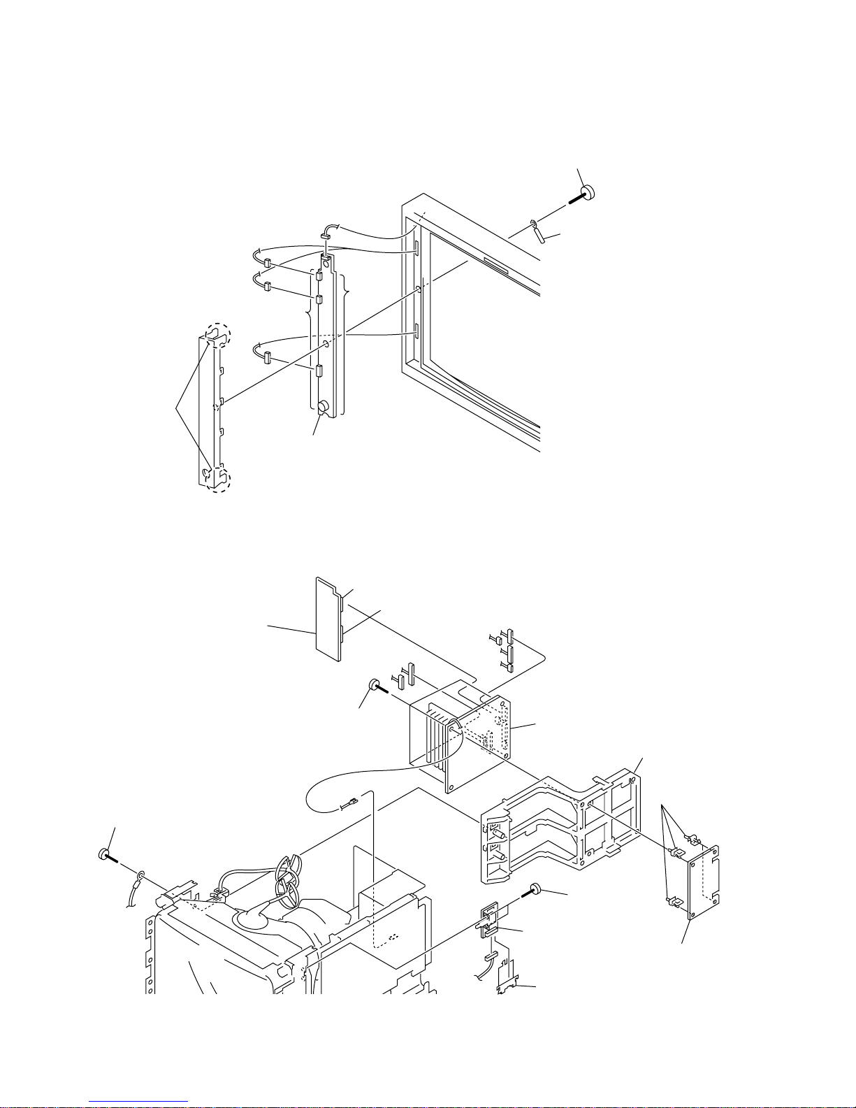
1-2-5. J , D1, D2 and D Boards Removal (14 inch)
CN1501
CN706
CN1508
CN1506
CN1507
CN1502
CN1503
6 Four screws
(+BVTP 3 x 12)
D board
5 Screw (+BVTT 4 x 8)
CN2502 (board to board)
4 D1 board
CN2501 (board to board)
1 Two screws
(+PSW 3 x 8)
2 Insulator (J PWB)
3 J board
CN951
9 Bracket D
8 D2 board
7 Four card edge
spacers
1-4
PVM-14L5/20L5/D14L5A/D20L5A
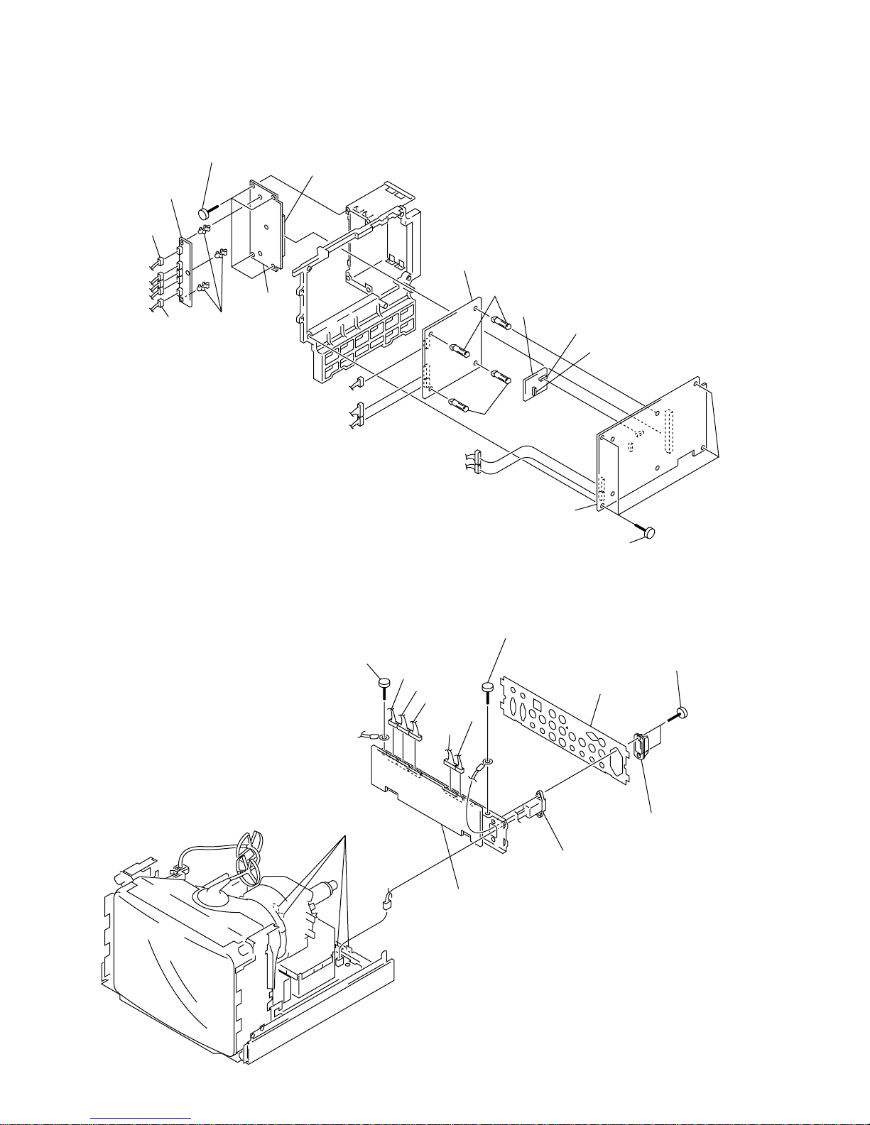
1-2-6. C Board Removal (14 inch)
CN705
CN704
CN702
CN701
CN703
C board
1-2-7. B Block Assy Removal (14 inch)
CN101
CN1906
CN1908
B block assy
CN2401
CN1905
CN1904
CN1903
CN1907
CN102
CN103
CN104
3 Screw (+PSW 4 x 8)
2 Three screws (+BVTP 3 x 12)
1 Screw (+BVTP 3 x 8)
1-5
PVM-14L5/20L5/D14L5A/D20L5A
1-2-8. K, T, B1, M and B Boards Removal (14 inch)
CN801
CN113
CN107 (board to board)
CN108 (board to board)
CN201
CN3802
CN3801
9 Four screws (+BVTT 3 x 8)
T board
1 Three PWB
holders
2 K board
7 Four screws
(+BVTP 3 x 12)
4 Two PWB
holders
3 Two PWB holders
5 B1 board
6 M board
8 B board
CN1901 (board to board)
CN3504
CN3505
CN3503
CN3502
CN3501
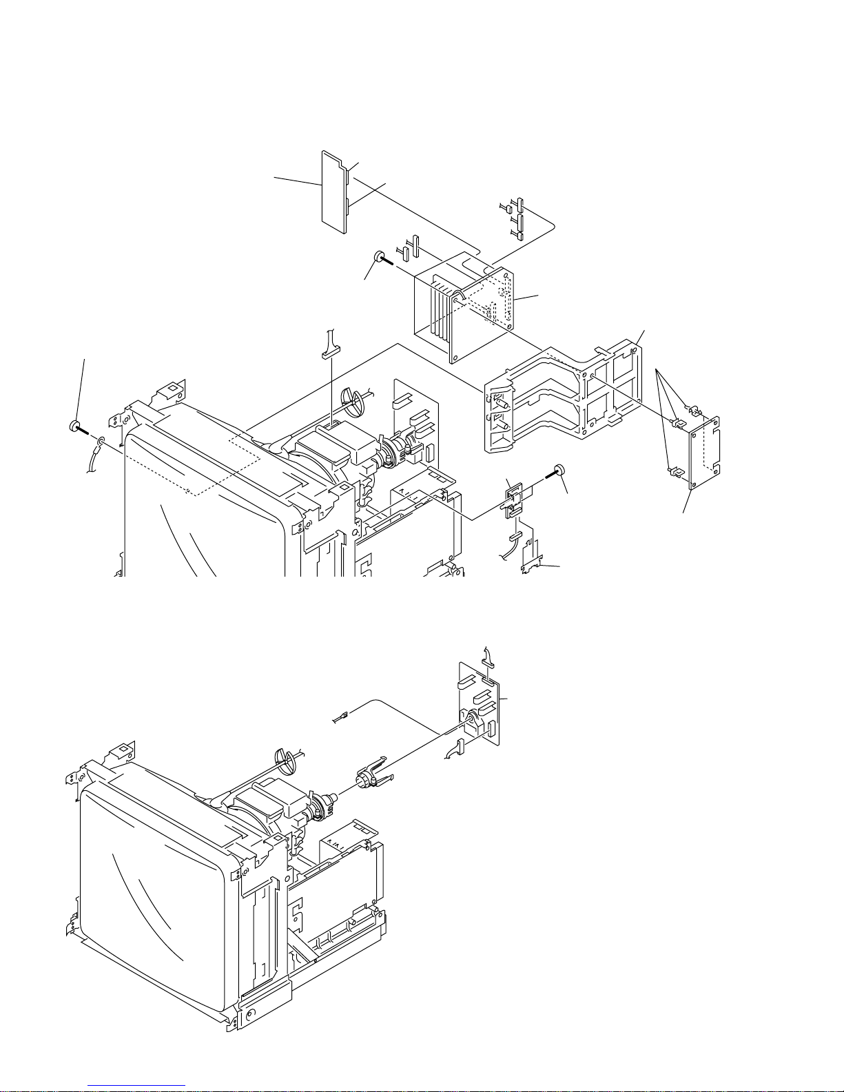
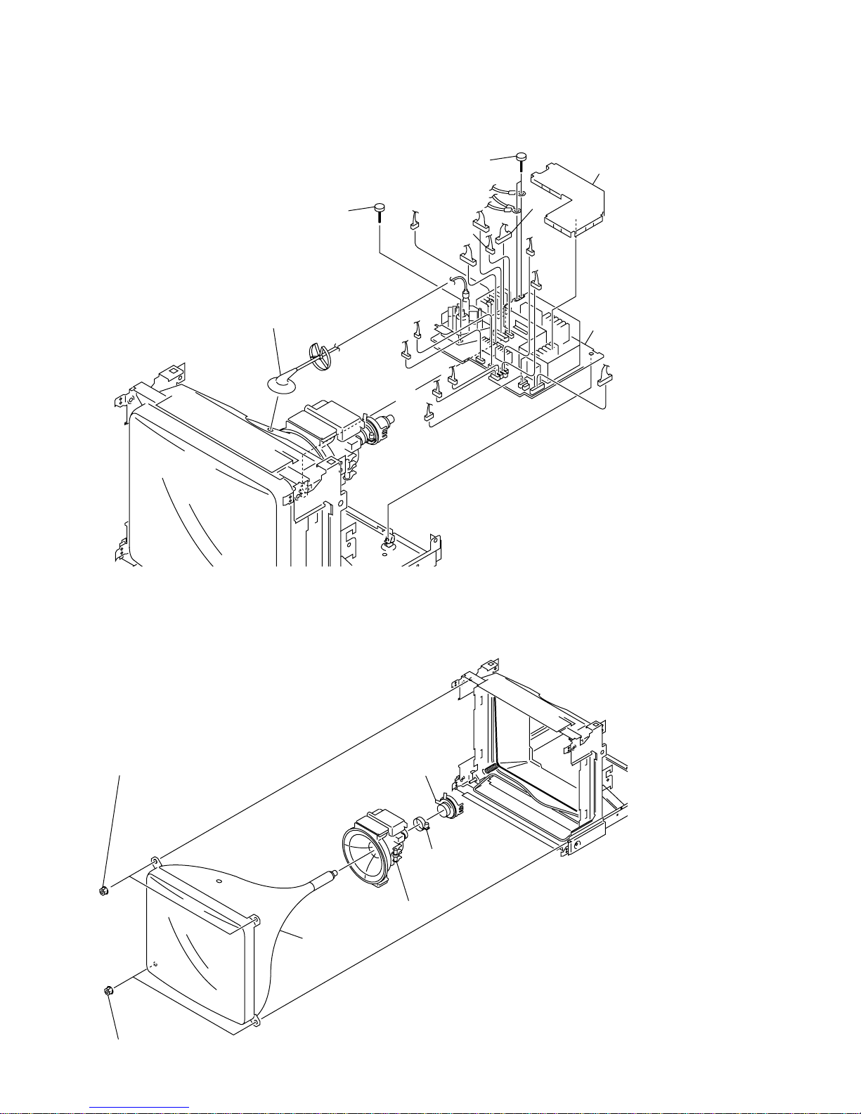
1-2-9. Q Block Assy Removal (14 inch)
CN2704
CN601
CN2706
CN2705
CN2707
CN2710
4 Two screws
(+PSW 3 x 12)
2 Four claws
1 Screw (+PSW 4 x 8)
3 Screw (+PSW 4 x 8)
6 Connector label
5 Plug holder (A)
7 AC inlet 3p (with noise filter)
8 Q block assy
1-6
PVM-14L5/20L5/D14L5A/D20L5A
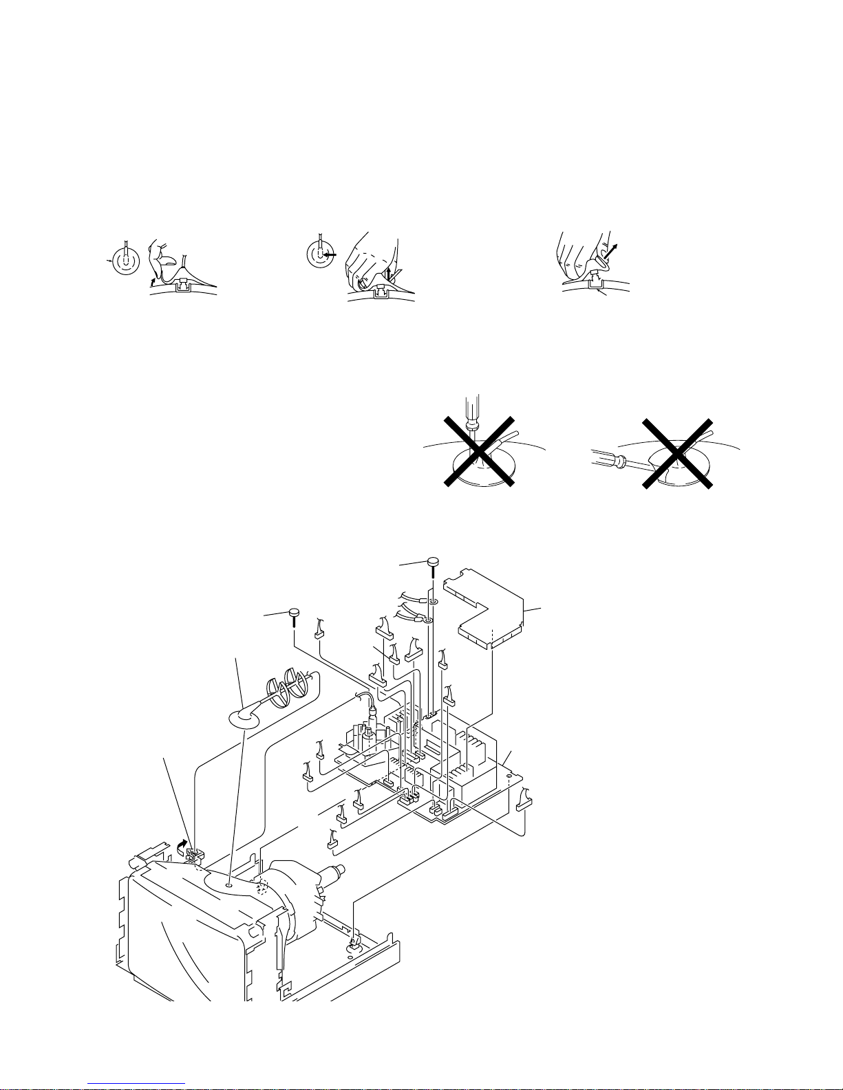
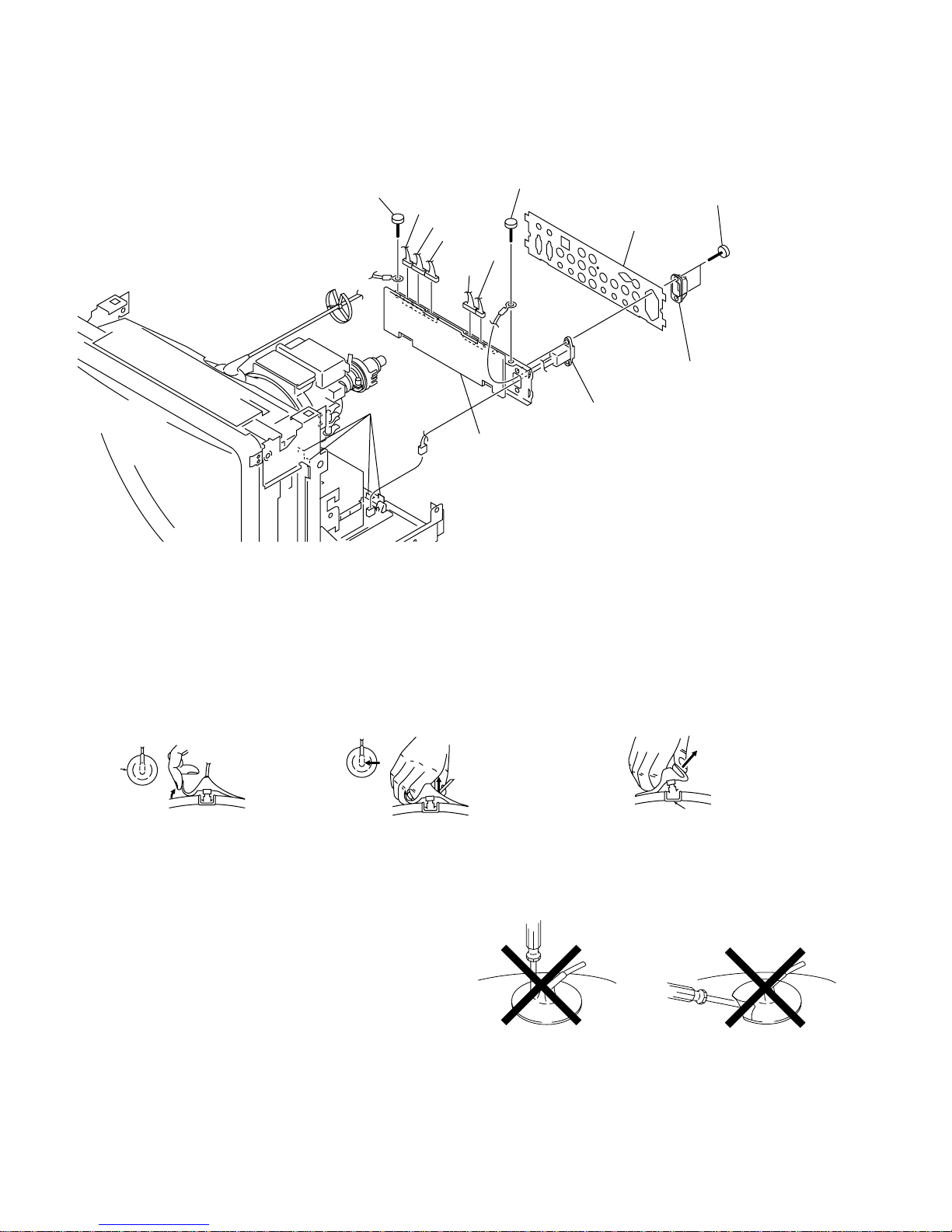
1-2-11.G Board Removal (14 inch)
4 Two screws (+PSW 4 x 8)
6 G shield
5 G board
CN602
CN603
CN610
CN609
CN604
CN608
CN608
CN607
CN503
CN606
CN607
CN508
CN505
1 Anode cap
2 Open the lead holder in the
direction of the arrow.
3
Screw (+BVTP 3 x 16)
(1) Turn up one side of the rubber cap in the
direction indicated by arrow a.
(2) Using a thumb, pull up the rubber cap
firmly in the direction indicated by
arrow b.
(3) When one side of the rubber cap is
separated from the anode button, the
anode-cap can be removed by turning
up the rubber cap and pulling up it in
the direction of the arrow c.
1-2-10.Removal of Anode Cap
n
Short-circuit the anode of the picture tube and the anode cap to the metal chassis, picture tube shield or carbon painted on
the picture tube, after removing the anode.
..
..
. Removal Procedure
..
..
. Handling Precautions
(1) Do not scratch the surface of anode cap with a sharp object.
(2) Do not press the rubber so hard that it damages the inside of
anode caps. A shatter-hook terminal is built into the rubber.
(3) Do not turn the foot of the rubber over.
The shatter-hook terminal will stick out or damage the rubber.
a
a
b
b
c
Anode button

1-7
PVM-14L5/20L5/D14L5A/D20L5A
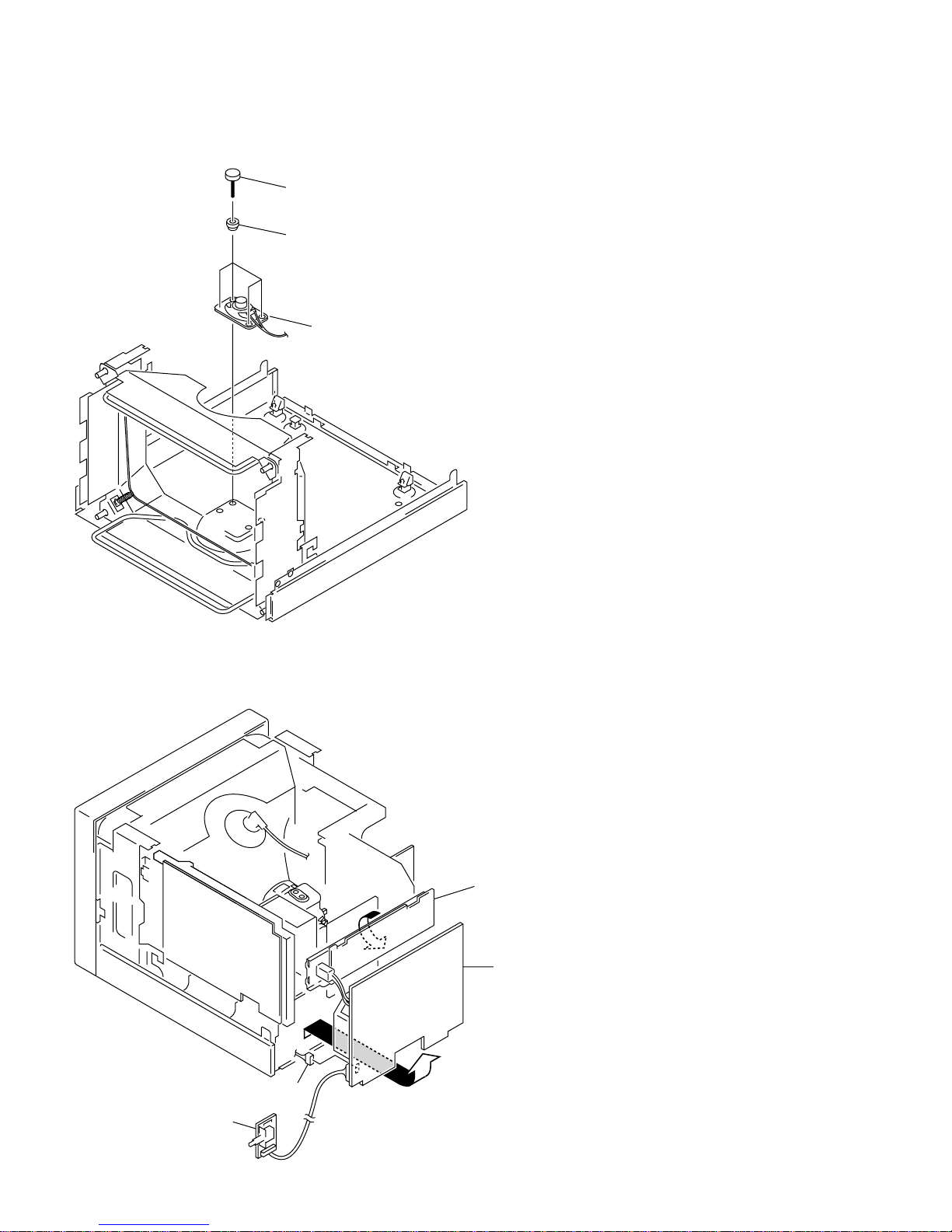
1-2-12. Picture Tube Removal (14 inch)
4 Two nuts (flange nut (B) M5)
6 Two nuts (flange nut (B) M5)
5 Two washers
(CRT position washer)
1 Fastening band assy
2 DY shield
7 Picture tube
3 Deflection yoke
1-8
PVM-14L5/20L5/D14L5A/D20L5A
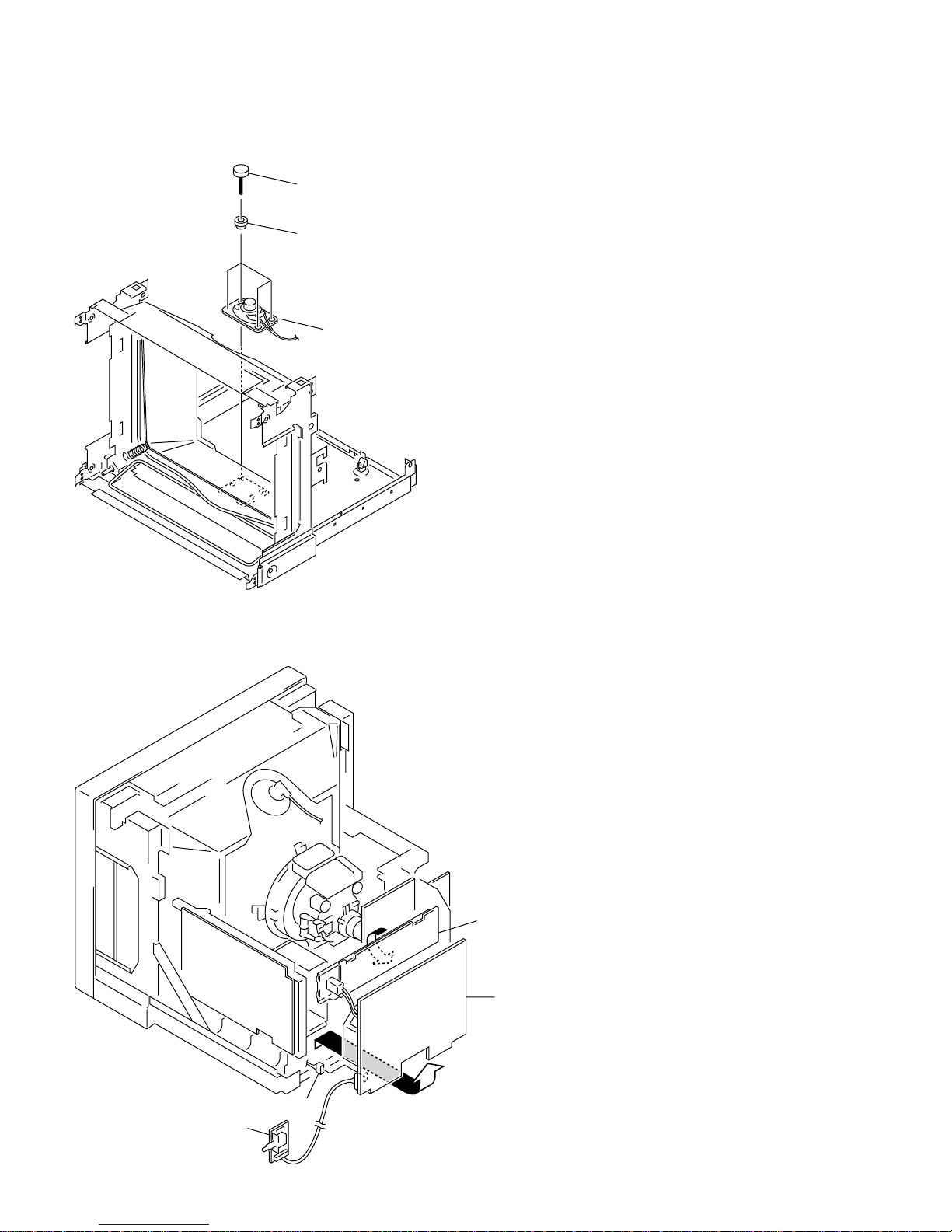
1-2-13.Speaker Removal (14 inch)
2 Four speaker cushions
3 Speaker
1 Four screws (step screw M3 x 4)
1-2-14.Service Position (14 inch)
CN603
G board
J board
Q board
*Because there exist the portions that have the high tension voltage,
be careful that the printed boards must not touch each other
nor must not touch with the chassis.
1-9
PVM-14L5/20L5/D14L5A/D20L5A
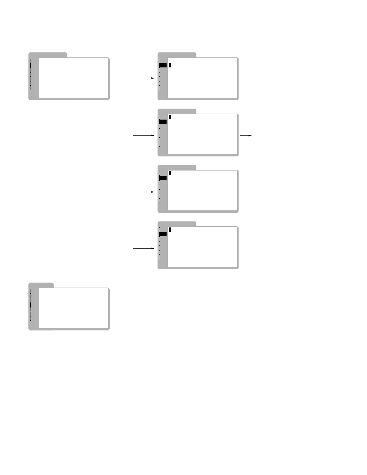
1-3. Board Layout (20 inch)
M
X
D1
B1
B
D
C
Q
G
T
HA
HB
K
J
D2
1-10
PVM-14L5/20L5/D14L5A/D20L5A
1-4. Disassembly (20 inch)
1-4-1. Top Cover Removal (20 inch)
4
1 Three screws
(claw case screw (OS))
2 Three screws
(claw case screw (OS))
3 Four screws
(+BVTT 4 x 8)
Top cover
Rear cover
1-4-2. Bezel Assy Removal (20 inch)
10 pin
10 pin
5 pin
9 pin
7 pin
2 Two screws
(+B 3 x 8)
3 Two screws (+B 3 x 8)
5 Shaft switch
1 Power button
6 Two claws
4
CN900
CN105
X board
Bezel assy
1-11
PVM-14L5/20L5/D14L5A/D20L5A
1-4-3. HA Board Removal (20 inch)
1 Three screws
(+BVTP 3 x 12)
2 Two wire holders
CN2902
CN2901
3 Four claws
4 Three
claws
5 Four claws
HA board
1-4-4. HB Board Removal (20 inch)
3 Control label (L)
CN5005
CN5002
CN5001
CN5004
4 Four claws
5 Four
claws
6 Four
claws
1 Four screws
(+BVTP 3 x 12)
HB board
2 Three wire holders
1-12
PVM-14L5/20L5/D14L5A/D20L5A
1-4-6. C Board Removal (20 inch)
CN702
CN701
CN704
C board
1-4-5. J, D1, D2 and D Boards Removal (20 inch)
CN1501
CN1508
CN1506
CN1507
CN1502
CN1503
CN2502 (board to board)
CN2501 (board to board)
CN951
6 Four screws
(+BVTP 3 x 12)
D board
5 Screw
(+BVTT 4 x 8)
4 D1 board
1 Two screws
(+PSW 3 x 8)
2 Insulator (J PWB)
3 J board
9 pin
9 Bracket D
8 D2 board
7 Four card edge
spacers
1-13
PVM-14L5/20L5/D14L5A/D20L5A
1-4-7. B Block Assy Removal (20 inch)
CN101
CN1906
CN1908
CN2401
CN1905
CN1904
CN1903
CN1907
CN102
CN103
CN104
3 Screw (+PSW 4 x 8)
2 Three screws
(+BVTP 3 x 12)
B block assy
1 Screw (+BVTT 4 x 8)
CN801
CN113
CN107 (board to board)
CN108 (board to board)
CN201
CN3802
CN3801
9 Four screws (+BVTT 3 x 8)
T board
1 Three PWB
holders
2 K board
7 Four screws
(+BVTP 3 x 12)
4 Two PWB
holders
3 Two PWB holders
5 B1 board
6 M board
8 B board
CN1901 (board to board)
CN3504
CN3505
CN3503
CN3502
CN3501
1-4-8. K, T, B1, M and B Boards Removal (20 inch)
1-14
PVM-14L5/20L5/D14L5A/D20L5A
(1) Turn up one side of the rubber cap in the
direction indicated by arrow a.
(2) Using a thumb, pull up the rubber cap
firmly in the direction indicated by
arrow b.
(3) When one side of the rubber cap is
separated from the anode button, the
anode-cap can be removed by turning
up the rubber cap and pulling up it in
the direction of the arrow c.
1-4-10.Removal of Anode Cap
n
Short-circuit the anode of the picture tube and the anode cap to the metal chassis, picture tube shield or carbon painted on
the picture tube, after removing the anode.
..
..
. Removal Procedure
..
..
. Handling Precautions
(1) Do not scratch the surface of anode cap with a sharp object.
(2) Do not press the rubber so hard that it damages the inside of
anode caps. A shatter-hook terminal is built into the rubber.
(3) Do not turn the foot of the rubber over.
The shatter-hook terminal will stick out or damage the rubber.
a
a
b
b
c
Anode button
1-4-9. Q Block Assy Removal (20 inch)
CN2704
CN601
CN2706
CN2705
CN2707
CN2710
4 Two screws
(+PSW 3 x 12)
2 Four claws
1 Screw (+PSW 4 x 8)
3 Screw (+PSW 4 x 8)
6 Connector label
5 Plug holder (A)
7 AC inlet 3p (with noise filter)
8 Q block assy
1-15
PVM-14L5/20L5/D14L5A/D20L5A
1-4-11.G Board Removal (20 inch)
3 Two screws (+PSW 4 x 8)
5 G shield
1 Anode cap
4 G board
2 Screw (+BVTP 3 x 16)
CN602
CN603
CN610
CN609
CN604
CN608
CN608
CN607
CN606
CN503
CN505
CN607
CN508
4 Two nuts (flange nut (B) M5)
5 Two nuts (flange nut (B) M5)
2 Neck assy
6 Picture tube
3 Deflection yoke
1 Fastening band
assy
1-4-12.Picture Tube Removal (20 inch)
1-16
PVM-14L5/20L5/D14L5A/D20L5A
1-4-14.Service Position (20 inch)
CN603
G board
J board
Q board
*Because there exist the portions that have the high tension voltage,
be careful that the printed boards must not touch each other
nor must not touch with the chassis.
1-4-13.Speaker Removal (20 inch)
2 Four speaker cushions
3 Speaker
1 Four screws (step screw M3 x 4)

2-1
PVM-14L5/20L5/D14L5A/D20L5A
Section 2
Set-up Adjustment
2-1. Equipment Required
. Oscilloscope
Sony Tektronix 2465 or equivalent (with bandwidth of
350 MHz)
. NTSC/PAL/SECAM component signal generator
Sony Tektronix TG2000 +AVG1 (option module)
+AWVG2 (option module) or equivalent
. SDI signal generator
Sony Tektronix TSG-422
. Monoscope signal generator
ShibaSoku TP22AX or equivalent
. VG (programmable video signal generator)
. VG814 or equivalent
. Frequency counter
Advantest TR5821AK or equivalent
. Digital VOM
Advantest TR6845 or equivalent
. Slide induction transformer
. High tension voltmeter
. DC power supply
. Ammeter
. Luminance meter
Minolta CA-110 or equivalent.
If the Minolta CA-110 is not available, perform the
measurement by visual inspection by comparing the
monitor that has already been adjusted earlier with the
monitor that you want to adjust.
n
Start the following adjustments after 5 minutes have
passed after the main power is turned on.
* In this chapter, [||||||] indicates the control items in the
service mode.
Example : [60|H-FREQ]
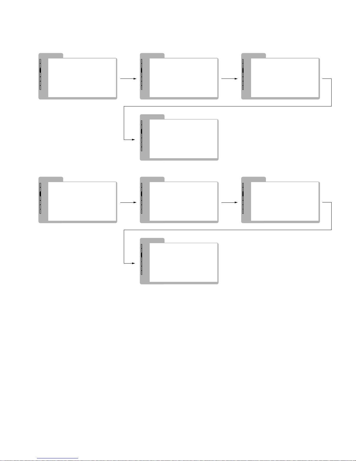
2-2. Preparations (1)
Service Mode
This set is provided with a switch for service on the front
panel that can be used to make various adjustments. The
operation method of this switch is explained in detail below.
1. Entering the service mode
Simultaneously press the [ENTER] key and the
[DEGAUSS] key shown on the display of the menu.
2. Operating the Service Mode
Select the desired service item with the [UP],
[DOWN] key and press the [ENTER] key to enter the
adjustment mode.
Press the [UP] key to increase the adjustment value.
Press the [DOWN] key to decrease the adjustment
value.
Press the [ENTER] key to save the adjustment value.
Press the [MENU] key to cancel the entry.
3. Finishing the service mode
Simultaneously press the [ENTER] key and the
[DEGAUSS] key shown on the display of the menu.
4. Easy ON/OFF of the service mode
If once entering the service mode after having turned
on the power, easy ON/OFF is possible by once more
pressing the LINE-A, LINE-B, RGB/COMP, OPT-A
or OPT-B switch on the front panel (the LED lights) as
long as the power is not turned off or as long as the
service mode is not finished.
SIGNAL
SIG
• LEVEL-1...
• LEVEL-2...
• WHITE BALANCE...
• DECODER COLOR...
• DECODER LEVEL...
• DETECTION...
DEF
OPT
REM
SYS
STA
ENG

2-2
PVM-14L5/20L5/D14L5A/D20L5A
5. Executing FACTROY LOAD
If the adjustment data is damaged or lost by some
reasons, you can restore the default factory adjustment
data by executing FACTROY LOAD as described
below.
Select the following submenus from the Service Menu
in the order of : [SYSTEM] → [FACTROY...] →
[LOAD...] to read the default factory data. If the
default factory data is damaged or the ROM is replaced without executing FACTORY SAVE as
described in the following paragraph, you cannot
execute FACTROY LOAD.
6. Executing FACTORY SAVE
This operation is to write the FACTROY LOAD data
into the factory data area in the memory.
Select the following submenus from the Service Menu
in the order of : [SYSTEM] → [MAINTENANCE ID]
and type 111. Then select the following submenus
from the Service Menu in the order of : [ENGINEER]
→ [FACTROY SAVE] to write the factory data in the
memory. FACTORY SAVE is protected from misoperation so that FACTORY SAVE cannot be executed unless MAINTENANCE ID is set.
FACTORY SET
If the following circuit board is replaced or the following
NVRAM on the respective board is replaced, perform the
following settings.
B board : IC104, IC108, IC109
B1 board: IC4804
1. Select the following submenus from the Service Menu
in the order of : [SYSTEM] → [MAINTENANCE ID]
and type 111.
2. Select the following submenus from the Service Menu
in the order of : [SYSTEM] → [MODEL GRADE] →
[MODEL TYPE] and write the model data of each
model in the [MODEL TYPE] referring to table 2-4.
3. If the NVRAM on the B board is replaced, select the
following submenus from the Service Menu : [ENGINEER] → [CLEAR NVM ON B] and write data.
4. If the NVRAM on the B1 board is replaced, select the
following submenus from the Service Menu : [ENGINEER] → [CLEAR NVM ON B1] and write data.
5. If any IC on the B board is replaced, perform all
adjustment items of the [SIGNAL] menu and of the
[DEFLECTION] menu.
If any IC on the B1 board is replaced, perform the
adjustment items of the [SIGNAL] → [DECODER
COLOR] and of [DECODER LEVEL] menus.
6. Upon completion of adjustment, select the menus
[ENGINEER] → [FACTORY SAVE] to save the
adjustment data.
2-3
PVM-14L5/20L5/D14L5A/D20L5A
SIGNAL
SIG
• LEVEL-1...
• LEVEL-2...
• WHITE BALANCE...
• DECODER COLOR...
• DECODER LEVEL...
• DETECTION...
DEF
OPT
REM
SYS
STA
ENG
LEVEL-1
SIG
• Y BLACK
• PB BLACK
• PR BLACK
• CHROMA PB
• CHROMA PR
• Y LEVEL
DEF
OPT
REM
SYS
STA
ENG
LEVEL-2
SIG
• G-Y/B LEVEL
• G-Y/R LEVEL
• PB LEVEL
• PR LEVEL
DEF
OPT
REM
SYS
STA
ENG
47
84
70
74
228
182
214
140
WHITE BALANCE
SIG
• SUB CONTRAST
• SUB BRIGHT
• COLOR TEMP
• MANUAL/AUTO
DEF
OPT
REM
SYS
STA
ENG
131
35
D65
AUTO
• START...
• X 313
• Y 329
• REF VALUE D65
WHITE BALANCE
SIG
• SUB CONTRAST
• SUB BRIGHT
• COLOR TEMP
• MANUAL/AUTO
DEF
OPT
REM
SYS
STA
ENG
131
35
D65
MANUAL
• ADJUST GAIN...
• ADJUST BIAS...
• ADJUST FINE...
DECODER COLOR
SIG
• HP
• CLP
• BURST GATE PLS
• XTAL F0
DEF
OPT
REM
SYS
STA
ENG
20
216
83
81
76
• SUB PHASE
• ACC PHASE 128
• R-Y PHASE 113
DECODER LEVEL
SIG
• DEC Y LEVEL
• DEC B-Y LEVEL
• DEC R-Y LEVEL
• ACC LEVEL
DEF
OPT
REM
SYS
STA
ENG
138
171
196
128
SIGNAL/DETECTION
SIG
• MACROVISION
DEF
OPT
REM
SYS
STA
ENG
ON
54
92
• CLP P DLY 225
Service Mode screen display
2-4
PVM-14L5/20L5/D14L5A/D20L5A
DEFLECTION
SIG
• FOCUS...
• RASTER H...
• RASTER V...
• GEOMETRY...
DEF
OPT
REM
SYS
STA
ENG
REMOTE
SIG
SERIAL
• BAUDRATE
• STOPBIT
• PARITY
38400
2BIT
EVEN
DEF
OPT
REM
SYS
STA
ENG
DEFLECTION
SIG
• H DUTY
• HFV SENSE
• HFV CONTROL
• H DF PHASE
• H DF PARA
• LANDING
• H PLL
25
62
250
34
18
128
LOCK
DEF
OPT
REM
SYS
STA
ENG
FOCUS
DEFLECTION
SIG
• H SIZE
• H CENTER
• H BLK LEFT
• H BLK RIGHT
• H BLK R FINE
• H POSITION
• MARKER SUB L
• MARKER SUB R
85
107
215
128
11
121
84
59
DEF
OPT
REM
SYS
STA
ENG
RASTER H
DEFLECTION
SIG
• V S LIN
• V C LIN
• TRAPEZOID
• SIDE PIN
• SIDE PIN W
• SIDE PIN BAL
• PARA CONTROL
• SIDE PIN S
13
24
28
36
32
16
16
24
DEF
OPT
REM
SYS
STA
ENG
GEOMETRY
DEFLECTION
SIG
• V SIZE
• V CENTER
• V BLK TOP
• V BLK BOTTOM
• OSD TIMING
84
142
82
196
0
DEF
OPT
REM
SYS
STA
ENG
RASTER V
H BLK R FINE is adjustable only
in 1080/60I and 1035/60I.
It is the fixed value in other modes.
2-5
PVM-14L5/20L5/D14L5A/D20L5A
SYSTEM
SIG
VERSION
• MODEL GRADE
• MODEL TYPE
• W/B DESCRIPTION...
• AGING MODE
• FACTORY...
• SIGNAL...
• MAINTENANCE ID
1.3
L4/L3
E14
0
DEF
OPT
REM
SYS
STA
ENG
SYSTEM
SIG
VERSION
• MODEL GRADE
• MODEL TYPE
• W/B DESCRIPTION...
• AGING MODE
• FACTORY...
• SIGNAL...
• MAINTENANCE ID
1.3
L4/L3
E14
0
DEF
OPT
REM
SYS
STA
ENG
SYSTEM
SIG
• COL2
• COL1 65
93
DEF
OPT
REM
SYS
STA
ENG
W/B DESCRIPTION
SYSTEM
SIG
• STANDARD...
• LOAD...
DEF
OPT
REM
SYS
STA
ENG
FACTORY
SYSTEM
SIG
• 720/50P
• 1080/48I
OFF
OFF
When OFF, 1080/48I is identified
as NO SYNC.
When OFF, 720/50P is identified
as NO SYNC.
LOAD cannot be selected and remains
in the blue display unless the NVM data is valid.
In such a case, clear the NVM and
make the NVM data valid first.
However, if the default factory data is damaged,
or if the FACTORY SET process is not executed
after ROM is replaced, LOAD cannot be executed.
STANDARD returns the various setups
of the user menu to the default factory setting.
DEF
OPT
REM
SYS
STA
ENG
SIGNAL
AGING MODE
All white screen
To return to the original screen,
press the button of the input selector
illuminating in orange.
2-6
PVM-14L5/20L5/D14L5A/D20L5A
STATUS
SIG
ADJUST ERROR
ABNORMAL I2C
NVM BOARD B
NVM BOARD B1
0
0
OK
OK
DEF
OPT
REM
SYS
STA
ENG
ENGINEER 1/3
SIG
• AUSP SAMPLE POS
• OE
• P SAVE
• DISPLAY
• D A
• D B
• H BLK1
1
0
1
0
1
0
• FACTORY SAVE...
• CLEAR NVM ON B...
• CLEAR NVM ON B1...
OFF
DEF
OPT
REM
SYS
STA
ENG
OPTION
SIG
BKM-129X
DEF
OPT
REM
SYS
STA
ENG
OPTION
SIG
BKM-120D (1/3)
DEF
OPT
REM
SYS
STA
ENG
• CCP P
• DA FV
• DB FV
• Y LEVEL
• PB LEVEL
• PR LEVEL
137
84
109
82
71
74
OPTION
SIG
BKM-120D (2/3)
DEF
OPT
REM
SYS
STA
ENG
• YB2
• YW0
• YW1
0
0
0
OPTION
SIG
BKM-120D (3/3)
DEF
OPT
REM
SYS
STA
ENG
ENGINEER 2/3
SIG
• DATA REFRESH
• SREM RAW DATA
• OSDLIMIT
• AWB ANA VALUE
• INTERNAL SIGNAL
ON
OFF
OFF
• 4:3MARKER LIMIT OFF
OFF
0
DEF
OPT
REM
SYS
STA
ENG
ENGINEER 3/3
SIG
• H SYNC COUNT
• MENU DOTCLOCK
• MENU H POS
• BLK H POS
• OPTION BOARD ID
HIDE
231
14
• BLK DOTCLOCK 231
8
255
DEF
OPT
REM
SYS
STA
ENG
OPTION (BKM-120D)
• 1125/60I SYS
• OE
• P SAVE
• DISPLAY
• IN1
• IN2
AUTO
1
0
0
0
0
OPTION
SIG
BKM-142HD 1/5
DEF
OPT
REM
SYS
STA
ENG
• YPBPR
• H BLK1
• H SUB
• Y LEVEL
• PB LEVEL
• PR LEVEL
1
240
128
120
22
28
OPTION
SIG
BKM-142HD 2/5
DEF
OPT
REM
SYS
STA
ENG
• SYSTA0
• SYSTA1
• P0
• P1
• P2
• P3
0
1
1
1
0
1
OPTION
SIG
BKM-142HD 3/5
DEF
OPT
REM
SYS
STA
ENG
• STRB
• SYCS1
• SYCS2
• SYIF0
• SYIF1
• SYIF2
1
1
0
1
1
1
OPTION
SIG
BKM-142HD 4/5
DEF
OPT
REM
SYS
STA
ENG
• SYIF3
• SYIF4
• SYIF5
• SYIF6
• SYIF7
1
0
0
0
0
OPTION
SIG
BKM-142HD 5/5
DEF
OPT
REM
SYS
STA
ENG
OPTION (BKM-142HD)
OPTION (BKM-129X)
2-7
PVM-14L5/20L5/D14L5A/D20L5A
• OE
• P SAVE
• DISPLAY
• D A
• D B
• H BLK1
0
0
1
0
1
0
OPTION
SIG
BKM-150CP (1/4)
DEF
OPT
REM
SYS
STA
ENG
• CCP P
• DA FV
• DB FV
• Y LEVEL
• PB LEVEL
• PR LEVEL
110
80
80
85
110
105
OPTION
SIG
BKM-150CP (2/4)
DEF
OPT
REM
SYS
STA
ENG
• SDTI SW
• TC MODE 0
• TC MODE 1
• TC MODE 2
• AUDIO MUTE
0
0
0
0
0
OPTION
SIG
BKM-150CP (3/4)
DEF
OPT
REM
SYS
STA
ENG
• AUDIO GRP 0
• AUDIO GRP 1
• AUDIO CH 0
• AUDIO CH 1
• AUDIO MIX
• AUDIO MONO L
1
1
0
1
1
0
• AUDIO MONO R 1
OPTION
SIG
BKM-150CP (4/4)
DEF
OPT
REM
SYS
STA
ENG
OPTION (BKM-150CP)
• OE
• V B
• V C
• BYPASS SW
• COMB SW
• ACC SW
0
1
1
OFF
ON
ON
OPTION
SIG
BKM-126M (1/4)
DEF
OPT
REM
SYS
STA
ENG
• PAL S SW
• APT SW
• PCD SW
• PAL SW
• KILLER
S
OFF
OFF
ON
0
OPTION
SIG
BKM-126M (2/4)
DEF
OPT
REM
SYS
STA
ENG
• Y LEVEL
• PB LEVEL
• PR LEVEL
• PHASE
• SUB PHASE
127
127
127
127
127
• BGP W 127
• ACC LEVEL 127
OPTION
SIG
BKM-126M (3/4)
DEF
OPT
REM
SYS
STA
ENG
• APT LEVEL
• CLP W
• R-Y PHASE
• ACC PHASE
• F0
127
127
127
127
127
OPTION
SIG
BKM-126M (4/4)
DEF
OPT
REM
SYS
STA
ENG
OPTION (BKM-126M)
2-8
PVM-14L5/20L5/D14L5A/D20L5A
Name Description Inch20 Inch14
HFV_SENS Horizontal frequency 15K 27 42
Horizontal frequency 27K 37 25
Horizontal frequency 28K 37 25
Horizontal frequency 31K 36 33
Horizontal frequency 33K 4 26
Horizontal frequency 37K 26 16
Horizontal frequency 45K 26 17
HFV_CONTROL Horizontal frequency 15K 249 250
Horizontal frequency 27K 200 200
Horizontal frequency 28K 200 200
Horizontal frequency 31K 180 188
Horizontal frequency 33K 177 177
Horizontal frequency 37K 160 160
Horizontal frequency 45K 128 128
H_SIZE 480/60I NORMAL 74 95
480/60I UNDER 49 71
575/50I NORMAL 78 102
575/50I UNDER 56 79
1080/48I NORMAL 77 106
1080/48I UNDER 55 82
1080/50I NORMAL 77 106
1080/50I UNDER 55 82
480/60P NORMAL 46 74
480/60P UNDER 32 50
576/50P NORMAL 54 81
576/50P UNDER 34 56
1080/60I 1035/60I NORMAL 41 64
1080/60I 1035/60I UNDER 21 44
720/50P NORMAL 41 64
720/50P UNDER 21 44
720/60P NORMAL 53 75
720/60P UNDER 30 51
H_CENT 480/60I 100 107
575/50I 100 107
1080/48I 100 107
1080/50I 100 107
480/60P 100 107
576/50P 100 107
1080/60I 1035/60I NORMAL 100 107
1080/60I 1035/60I UNDER 100 107
720/50P 100 107
720/60P 100 107
Name Description Inch20 Inch14
H_POSITION 480/60I 82 85
575/50I 74 77
1080/48I 64 70
1080/50I 64 70
480/60P 83 89
576/50P 80 85
1080/60I 1035/60I NORMAL 92 101
1080/60I 1035/60I UNDER 92 101
720/50P 79 86
720/60P 79 86
SIDE_PINBAL 480/60I 4:3 NORMAL 18 19
480/60I 4:3 UNDER 18 23
480/60I 16:9 NORMAL 14 18
480/60I 16:9 UNDER 18 19
575/50I 4:3 NORMAL 14 15
575/50I 4:3 UNDER 16 15
575/50I 16:9 NORMAL 16 15
575/50I 16:9 UNDER 16 17
1080/48I NORMAL 16 17
1080/48I UNDER 16 14
1080/50I NORMAL 16 17
1080/50I UNDER 16 14
480/60P 4:3 NORMAL 15 13
480/60P 4:3 UNDER 16 16
480/60P 16:9 NORMAL 15 14
480/60P 16:9 UNDER 16 14
575/50P 4:3 NORMAL 15 16
575/50P 4:3 UNDER 15 15
575/50P 16:9 NORMAL 16 14
575/50P 16:9 UNDER 15 16
1035/60I NORMAL 14 15
1035/60I UNDER 16 14
1080/60I NORMAL 14 15
1080/60I UNDER 16 14
720/50P NORMAL 15 14
720/50P UNDER 15 15
720/60P NORMAL 15 14
720/60P UNDER 15 15
PARA_CONTROL 480/60I 4:3 NORMAL 13 14
480/60I 4:3 UNDER 14 15
480/60I 16:9 NORMAL 14 15
480/60I 16:9 UNDER 14 15
575/50I 4:3 NORMAL 11 16
 Loading...