

Sony Trinitron Multiscan CPD-1302 Service Manual
SERVICE
August,
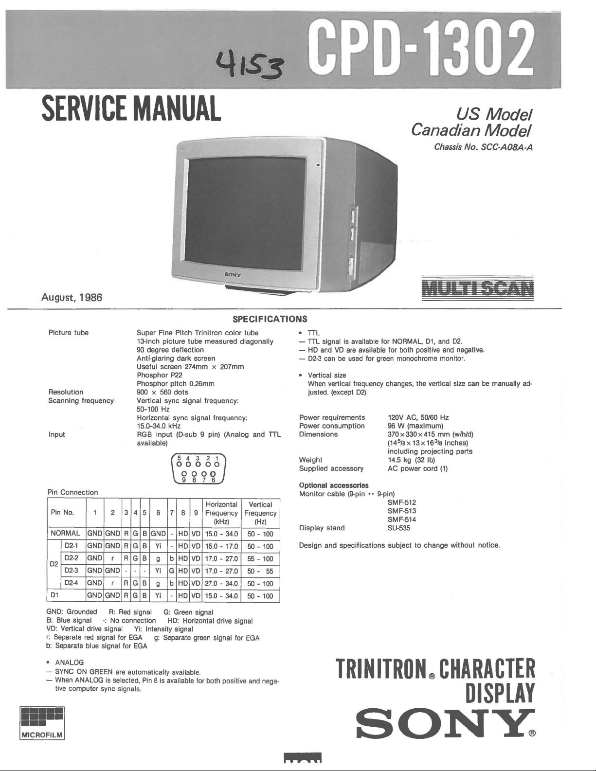
Picture tube
Resolution
Scanning frequency
Input
1986
MANUAL
Super Fine Pitch Trinltron color tube
13-lnch picture tube measured diagonally
90
degree deflection
Anti·glaring dark screen
Useful screen 274mm x 207mm
Phosphor
Phosphor pitch 0.26mm
900 x 560
Vertical sync signal frequency:
50-100 Hz
Horizontal sync signal frequency:
15.0-34.0 kHz
RGB
available)
P22
dots
input (D·sub 9 pin) (Analog and TTL
SPECIFICATIONS
• TTL
- TTL
-
-
• Vertical size
Power requirements
Power consumption
Dimensions
Weight
Supplied accessory
Canadian Model
_
-
l*i
signal is available for NORMAL,
HD
and
VD
are
D2-3
can
When
vertical frequency changes, the vertical size can
justed. (except
available for both positive
be
used
for
green
D2)
120V AC,
96
370x330x415
(14
including projecting parts
14.5
AC power cord
D1,
monochrome monitor.
50/60
W (maximum)
5
x
13
X 16
/8
kg
(32
Ib)
US
Chassis
...
_
...
_._------
i=
1:
~ E E-~l.E=j':'
and
D2.
and
negative.
Hz
mm (w/h/d)
3
18
Inches)
(1)
Model
No. SCC·AOBA·A
...
- -
be
manually
--
~
i.._
ad-
Pin
Connection
Pin
No.
NORMAL
D2
D1
GND:
B:
Blue signal
VD
: Vertical drive signal
r: Separate
b:
Separate blue signal for
• ANALOG
-
SVNC
-
When
tive computer sync signals.
D2·1
D2-2
D2-3
D2-4
Grounded
red
ON
ANALOG
1 2
GND
GND
GND
GND
GND
GND
-:
signal for
GREEN
GND
GND
r
GND
r
GND
R:
No connection
are
is
selected,
3
4
5
6 7 8 9 Frequency
R G B
GND
R G B
R
R G B g b
R G B
Red
Vi
g
G B
signal
Vi:
EGA
EGA
automatically available.
b
Vi
G
Vi
-
G:
Green
HD:
IntenSity signal
g:
Separate
Pin
8 is available
Horizontal
(kHz)
HD
VD
15.0 -34.0
HD
VD
15.0 -17.0
HD
VD
17.0 -27.0
HD
VD 17.0 -
HD
VD 27.0 -
HD
VD
signal
Horizontal drive signal
green
15.0 -34.0
Signal
for
both positive
27.0
34.0
for
Vertical
Frequency
(Hz)
50 -100
50
-
100
55 -100
55
5050
-
100
50 -100
EGA
and
nega
Optional accessories
Monitor cable (g.pin ... g.pln)
Display stand
Design and specifications subject
-
TRINITRON®
SONY:
iiBCtl
SMF-512
SMF-513
SMF-514
SU-535
to
change without notice.
CHARACTER
DISPLAY
CPD-130
2 1
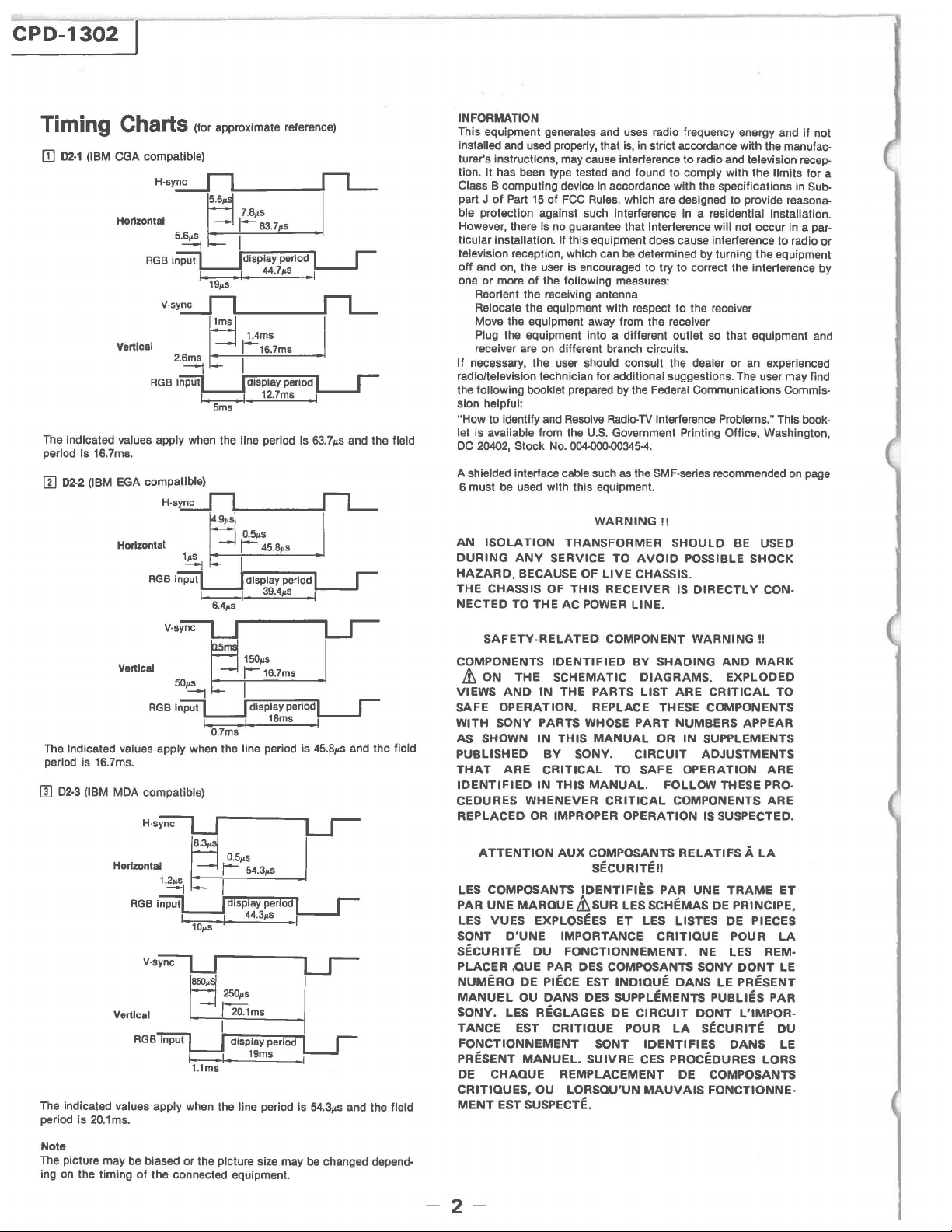
Timing Charts (for approximate reference)
[]
D2·1
(IBM
CGA
compatible)
The Indicated values apply when the line period
period
Is
16.7ms.
rn
D2·2
(IBM
EGA
compatible)
Is
63.7I's and the field
INFORMATION
This equipment generates
installed
and
turer's instructions, may cause interference to radio
tion. It has
Class B computing device
part J
ble
However, there
ticular installation. If
television reception, which can
off and on, the user is encouraged to try to correct the interference by
one or more
Reorient the receiving antenna
Relocate the equipment with respect to the receiver
Move the equipment away from the receiver
Plug the equipment into a different outlet
receiver are on different branch circuits.
If necessary, the user should consult the dealer or an experienced
radloltelevlslon technician for additional suggestions.
following booklet prepared
the
slon helpful:
"How
is available from the
let
DC
20402,
A shielded interface cable
6 must
AN
DURING
HAZARD,
THE CHASSIS OF THIS
NECTED
used
been
type tested
of
Part
15
protection against such interference
to identify
be
ISOLATION
of
Is
no guarantee that Interference will not occur in a par·
of
the following measures:
and
Stock
No.
used with this equipment.
ANY
SERVICE TO
BECAUSE OF
TO THE AC POWER LlNE_
and
properly, that
FCC
this equipment does cause interference to radio
Resolve
0Q4.()()(J.()()345-4.
TRANSFORMER
uses radio frequency energy and
is,
in
strict accordance with the manufac·
and
found to comply with the limits for a
In
accordance with the specifications in
Rules,
which
are
designed to provide reasona·
be
determined by turning the equipment
by
the Federal Communications Commls·
Radio-TV
U.S.
such
WARNING
LIVE
RECEIVER
Interference Problems." This book·
Government Printing Office, Washington,
as
the SMF·series recommended
!!
SHOULD
AVOID
CHASSIS_
IS
and
television recep·
In
a residential installation.
so
that equipment and
The
user may find
BE
POSSIBLE SHOCK
DIRECTLY
USED
CON·
on
if
not
Sub-
page
or
rn
02·3
(IBM
MOA
compatible)
H-sync
Horizontal
1.~
250pS
1--1.
Urns
I 20.1rns
display period
19rns
Vertical
The
indicated values apply when the line period Is
period is
20.1
ms.
54.3JLS
and the field
SAFETY·RELATED
COMPONENTS
&.
ON
VIEWS
SAFE OPERATION. REPLACE THESE COMPONENTS
WITH
AS SHOWN
PUBLISHED
THAT
IDENTIFIED
CEDURES
REPLACED
LES COMPOSANTS
PAR
LES
SONT
SECURITE
PLACER
NUMERO
MANUEL
SONY.
TANCE
PRESENT
DE
CRITIQUES,
MENT
AND
SONY PARTS WHOSE
ARE
ATTENTION
UNE
VUES
D'UNE
LES REGLAGES
FONCTIONNEMENT
CHAQUE
EST SUSPECTE.
IDENTIFIED
THE
SCHEMATIC
IN
IN
THIS
BY
CRITICAL
IN
THIS
WHENEVER
OR IMPROPER
AUX
MARQUE&'SUR
EXPLOSEES
DU
.QUE PAR DES COMPOSANTS SONY
DE
PIECE EST
OU DANS DES SUPPLEMENTS
EST
CRITIQUE
MANUEL.
OU LORSQU'UN
COMPONENT
BY
SHADING
THE PARTS
SONY.
MANUAL.
COMPOSANTS
SECURITEII
IDENTIFIES
IMPORTANCE
FONCTIONNEMENT.
SUIVRE
REMPLACEMENT
DIAGRAMS.
LIST
PART
MANUAL
CRITICAL
SONT
OR
CIRCUIT
TO
SAFE
FOLLOW THESE PRO·
OPERATION
PAR
LESSCHEMAS
ET
LES LISTES DE PIECES
CRITIQUE
INDIQUE
DE
CIRCUIT
POUR
IDENTIFIES
CES PROCEDURES LORS
MAUVAIS
WARNING
ARE
CRITICAL
NUMBERS APPEAR
IN
SUPPLEMENTS
ADJUSTMENTS
OPERATION
COMPONENTS
IS SUSPECTED.
RELATIFS A LA
UNE
NE LES REM·
DANS
PUBLIES
DONT
LA
SECURITE
DE COMPOSANTS
FONCTIONNE·
!!
AND
MARK
EXPLODED
TRAME
DE PRINCIPE,
POUR
LE
DANS
TO
ARE
ARE
DONT
PRESENT
PAR
L'IMPOR·
DU
ET
LA
LE
LE
Note
The
picture may
ing
on
the timing
be
biased or the picture size may
of
the connected equipment.
be
changed depend·
-2-
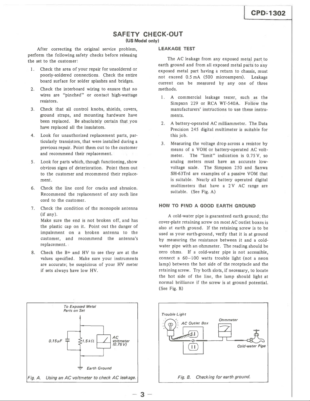
SAFETY CHECK-OUT
(US
Model
only)
After correcting the original service problem, LEAKAGE TEST
perform the following safety checks before releasing
the set
to
the customer:
Check the area
1.
poorly-soldered connections. Check the entire
board surface for solder splashes and bridges.
Check the interboard wiring to ensure that no
2.
wires are
resistors.
3. Check
ground straps, and mounting hardware have
been replaced.
have replaced all the insulators.
4. Look for unauthorized replacement parts, particularly transistors,
previous repair.
and recommend their replacement.
5. Look for parts which, though functioning, show
obvious signs
to the customer and recommend their replacement.
6. Check the line cord for cracks and abrasion.
cord to the customer.
7. Check the condition
(if
the plastic cap
replacement . .
8.
that
Recommend the replacement
a:ny).
Make sure the end
impalement
customer, and recommend the antenna's
Check the
values specified. Make sure your instruments
are accurate; be suspicious
if sets always have low HV.
of
your
repair for unsoldered
"pinched"
all control knobs, shields, covers,
of
on
B+
or contact high-wattage
Be
absolutely certain that
that
were installed during a
Point them
deterioration. Point them
on
it. Point
a broken antenna
and
out
to
the
of
any such line
of
the monopole antenna
is
not
broken off, and has
out
the danger
HV
to see they are at the
of
your
customer
HV
to
meter
or
you
out
of
the
The
earth ground and from all exposed metal parts
exposed metal part having a return
not exceed
current can be measured by
methods.
I.
A commercial leakage tester, such
Simpson 229 or
manufacturers' instructions to use these instruments.
2. A battery-operated
Precision 245 digital multimeter
this job.
3. Measuring the voltage drop across a resistor by
means
meter. The
analog meters must have an accurate lowvoltage scale. The
SH-63Trd are examples
is suitable. Nearly all battery operated digital
multimeters that have a 2 V
suitable.
HOW TO
A cold-water pipe
cover-plate retaining screw
also at earth ground.
used
as
by measuring the resistance between
water pipe with an ohmmeter. The reading should be
zero ohms.
connect a
lamp) between the hot side
retaining screw. Try
the
hot
normal brilliance if the screw
(See Fig.
AC
leakage from any exposed metal part
to
0.5
mA
(500 microampers). Leakage
anyone
RCA
Wf-540A. Follow the
AC
milliammeter. The Data
is
of a YOM
(See Fig. A)
FIND
or
battery-operated
"limit"
A GOOD EARTH GROUND
indication
Simpson 250 and Sanwa
of
a passive
AC
is
guaranteed earth ground; the
on
most
AC
outlet boxes is
If the retaining screw is to be
your earth-ground, verify
If a cold-water pipe is
60- 100 watts trouble light
both
slots,
side
of
the line, the lamp should light
B)
that
it is at ground
it
not
of
the receptacle and the
if
necessary,
is
at ground potential.
CPD-1302
to
to
any
chassis, must
of
three
as
the
suitable for
AC
volt-
is
0.75
V,
so
YOM
that
range are
and a cold-
accessible,
(not
a neon
to
locate
at
Fig.
A. Using an
To
Exposed
Parts
AC
Metal
on
Set
-=-
Earth Ground
voltmeter to check
AC
voltmeter
(0.75
V)
AC
leakage.
- 3 -
Trouble Light
-:
AC
Outlet
Box
_~_-t-@
Fig.
B.
I
Checking
Onmmeter
for
earth ground.
Cold-water Pipe
CPD-1302
TABLE OF CONTENTS
Section
1.
GENERAL
1-1. Location and Function
1-2. Connections
Use
of
1-3.
a Display Stand
Title
.......................
2. DISASSEMBLY
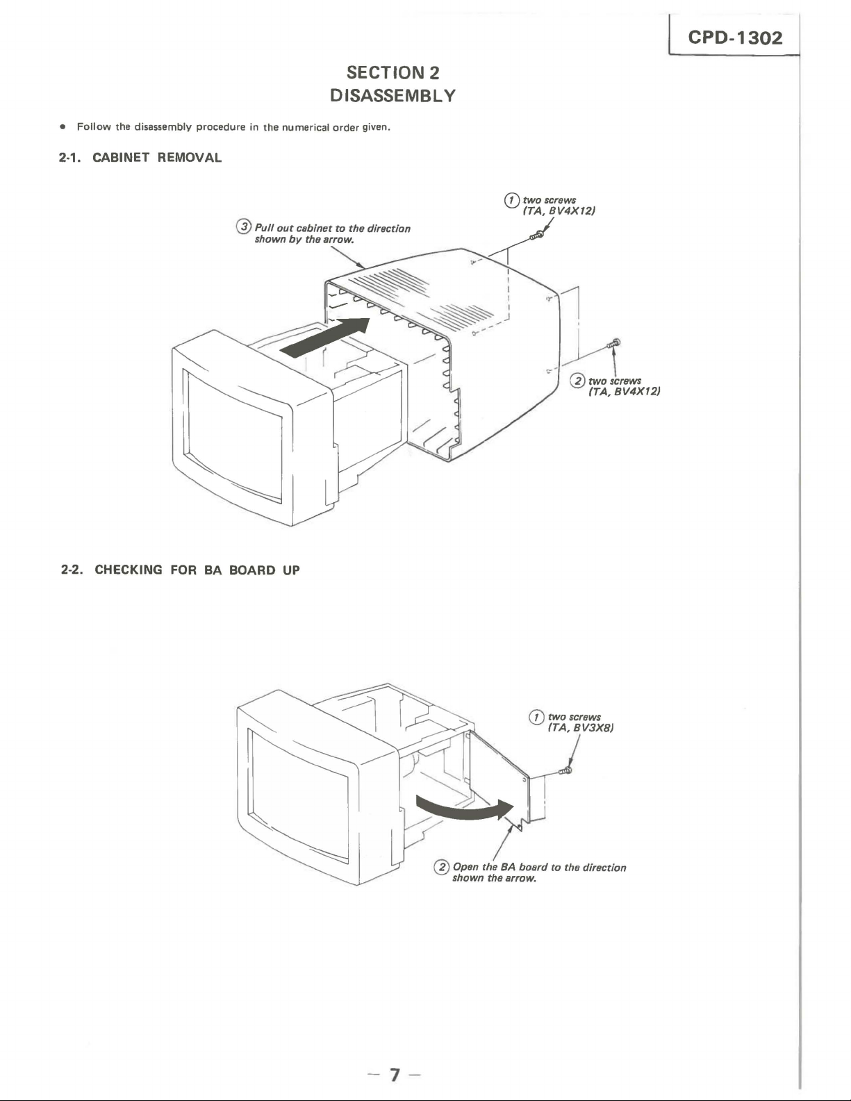
2-1. Cabinet Removal
2-2. Checking for
2-3. Checking for G and F Boards
2-4. Checking for
2-5. Checking for
2-6. Checking for H and
2-7. Picture Tube Removal . .
3.
SAFETY
RE
LATED ADJUSTMENT . . . . . . 11, 12
......
BA
board Up
BA
board Up
CA
board Up
BB
of
controls
................
.
.............
.............
Up
.............
.............
boards Up
..
......
........
.........
........
.
Page
Section Title
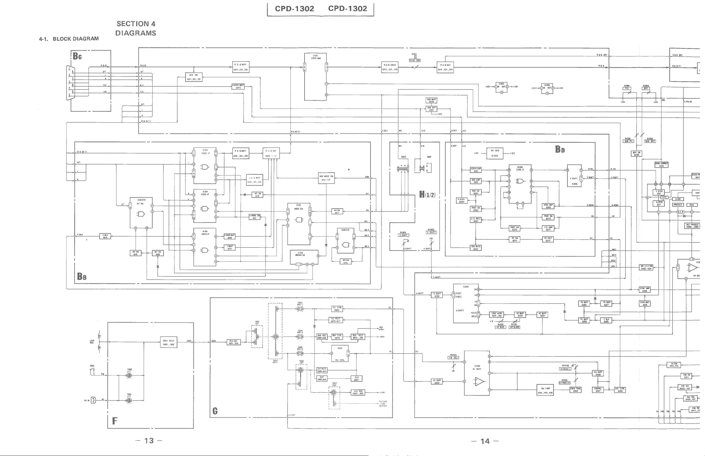
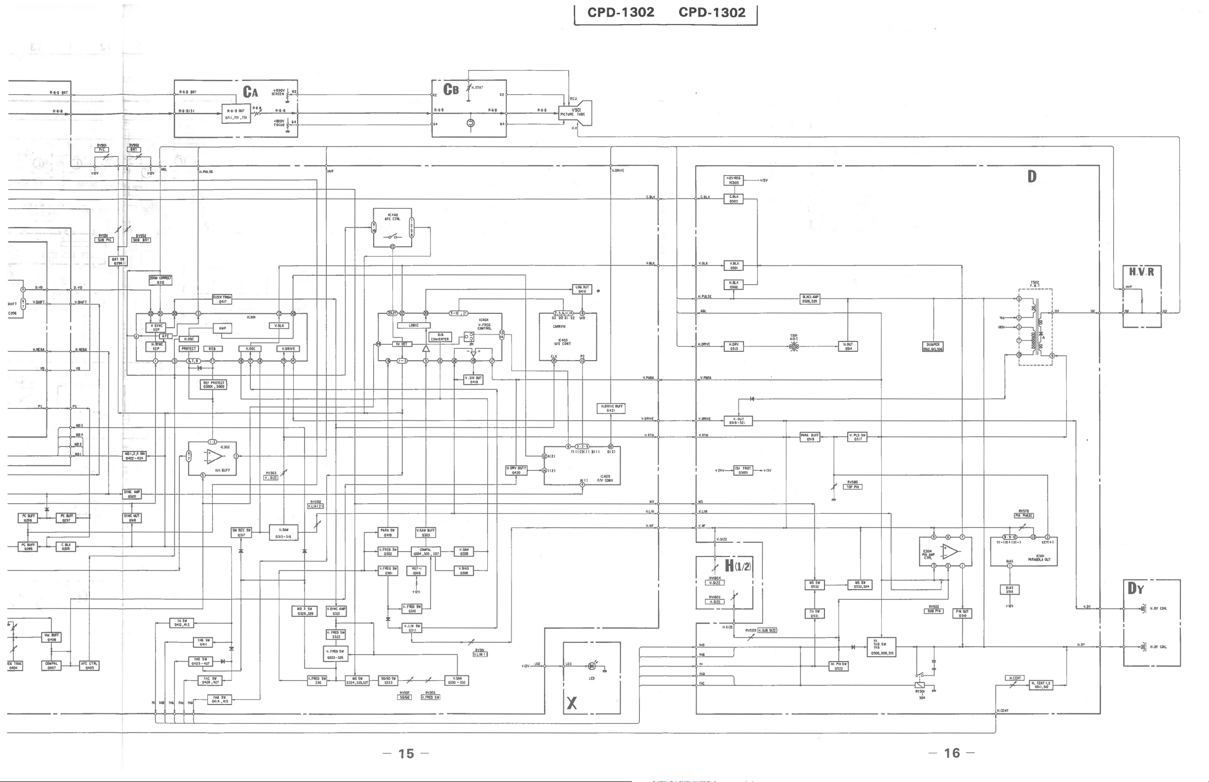
4. DIAGRAMS
5
6
6
7
7
8
8
9
9
....
10 6. ELECTRICAL PARTS LIST .
4-1. Block Diagram . . . . . . . . . . . . . . . . . . . .
4-2. Circuit Boards Location
4-3. Schematic Diagrams
4-4. Printed Wiring Boards
4-5.
Wave
Form
4-6. Semiconductors
5. EXPLODED VIEWS
5-1. Picture Tube
5-2. Chassis Assy
........
...................
.......
......
..............
.................
..............
.
..............
.
..............
.
...............
..........
13
17
17
. .
25
33
35
36
37
.
...
36
-4-
,-,_
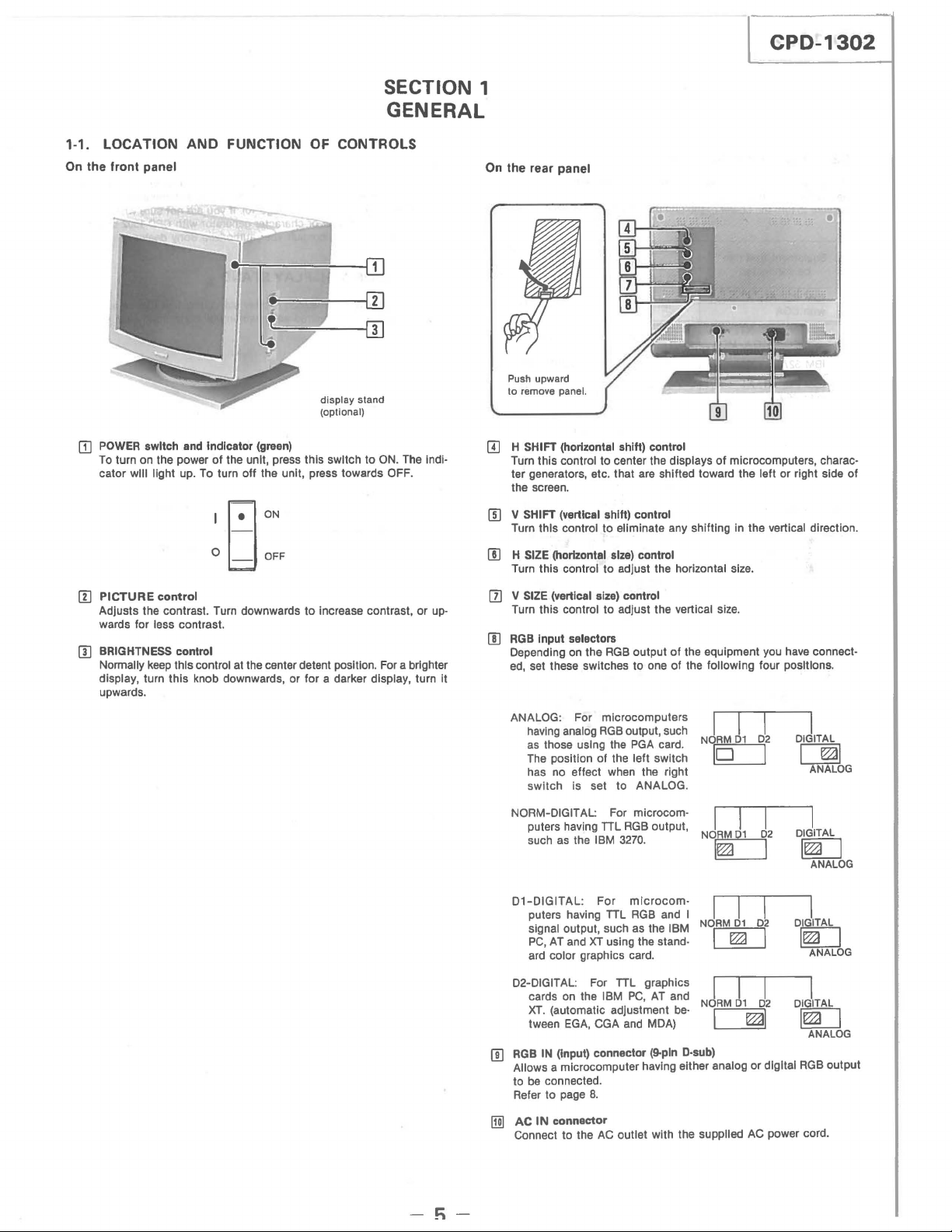
LOCATION
On
the
Iront
m
POWER
To
turn on the power
cator will light up.
panel
switch
AND
FUNCTION OF CONTROLS
I
~~
j
""==---:
=------1[!]
display stand
(optional)
and
indicator
To
(green)
of
the unit, press this switch to
turn off the unit, press towards
SECTION 1
GENERAL
.r----,rn
ON.
The
Indi-
OFF
.
On
the
rear
panel
Push upward
to remove
panel.
m H SHIFT (horizontal shift) control
Turn this control to center the displays
ter generators, etc. that
the screen.
are
shifted toward the left or right side of
CPO-1302
of
microcomputers, charac-
0N
8
o
ld
OFF
rn
PICTURE
Adjusts the contrast. Turn downwards to increase contrast, or
wards for less contrast.
rn
BRIGHTNESS control
Normally
display, turn this knob downwards,
upwards.
control
keep
this control
at
the center detent position.
or
for a darker display, turn It
For
a brighter
up-
[[)
V SHIFT (vertical shift) control
Turn this control to eliminate any shifting in the vertical direction.
[I]
H
SIZE
(horizontal size) control
Turn
this control to adjust the horizontal
rn
V
SIZE
(vertical size) control
Turn this control to adjust the vertical size.
[[)
RGB
Input selectors
Depending
ed,
ANALOG: For microcomputers
NORM-DIGITAL:
on
the
analog
effect
the
RGB
RGB
output, such
when
For microcom-
TIL
RGB
IBM
3270
set these switches to
having
as
those using the
The
position of the left switch
has
no
switch is set to
puters having
as
such
output
of
the equipment
one
of the following four positions.
PGA
card.
the right
ANALOG.
output,
.
size.
you
have
DIGITAL
C@]
DIGITAL
W£J
D1-DIGITAL:
puters having
signal
PC,
AT
ard
color graphics card.
For mIcrocom-
TIL
output, such
and
XT
using the stand·
RGB
as
and
the IBM
I
NORM 01
1 1
I
~
012
I
connect-
I
ANALOG
I
ANALOG
-fi-
D2-DIGITAL: For
ill
RGB
Allows a microcomputer having either analog or digital
to
Refer to
11m
AC
Connect to the
on
cards
XT
. (automatic adjustment
tween
EGA,
IN
(Input) connector
be
connected.
page
IN
connector
TIL
the
CGA
8.
AC
graphics
IBM
PC,
AT
and
MDA)
(S-pln
outlet with the supplied
and
be·
NORM 01
D-sub)
d2
~I
AC
power cord.
RGB
output

;:PD-1302
1·2. CONNECTIONS
Use
an
appropriate optional color monitor cable with 9-pln D·sub con·
nectors shown
Be
sure to turn the power
Equipment that can
IBM
with CGA
IBM
with
IBM
IBM
with
Microcomputer
in
the table.
be connected
PC,
·AT,
XT
PC,
AT,
PGA
CGA,
AT,
XT
XT
Set
positions.
EGA,
3270
PC,
of
the unit off before making any connections.
Monitor cable
(optional) input selectors
to be used
SMF·512
MDA
to
appropriate :
SMF·512 D2·DIGITAL
SMF·514 NORM·DIGITAL
SMF·513 ANALOG
-;'''''
Rear of the CPD·I302
',r,:-
IL
"':
""''''+='''~
Position
of
_____
o
o
'''
'''=:'-
____
AC
cord (supplied) outlet
of
RGB
the
CPD·1302
D1·DlGITAL
~II
...JI
AC
..
power
to a
to the
Input connector
power wall
Note
The monitor cable should arrange the
nected equipment so that they match the signal assignment of the
IN
connector of this unit
can use your computer or character generator with
cable to use, consult your authorized Sony dealer.
monitor
1-3.
USE
OF
With the optional Sony
be
viewed at your desired angle within
to
tically.
For details, read the instructions of the display stand,
(See
page
A DISPLAY STAND
SU·535
RGB
output signals of the con·
10).
If you are not sure whether you
display stand, this unit can
goo
15°
CPD·1302
horizontally and 15° ver.
or
be
adjusted
RGB
which
1 Align the plug with the receptacle. 2 Plug in and tighten the
~
,
To
disconnect the plug, loosen the screws,
screws.
~
-6-
, •
•
Follow
2
.1. CABINET REMOVAL numerical
d'~'''mblv
h . OISA
procedure ·
@Pulloutcab·
In
the
sh
own
by
the
SECTION 2
order
given.
met
to
th .
arrow.
e direction
SSEMBLY
(f) two screws
~V4"12)
2·2. CHECKING
FOR
BA
BOARD
UP
@OpentheB
show
'"
board t n the arrow. a the direction
- 7 -
CPD-1302
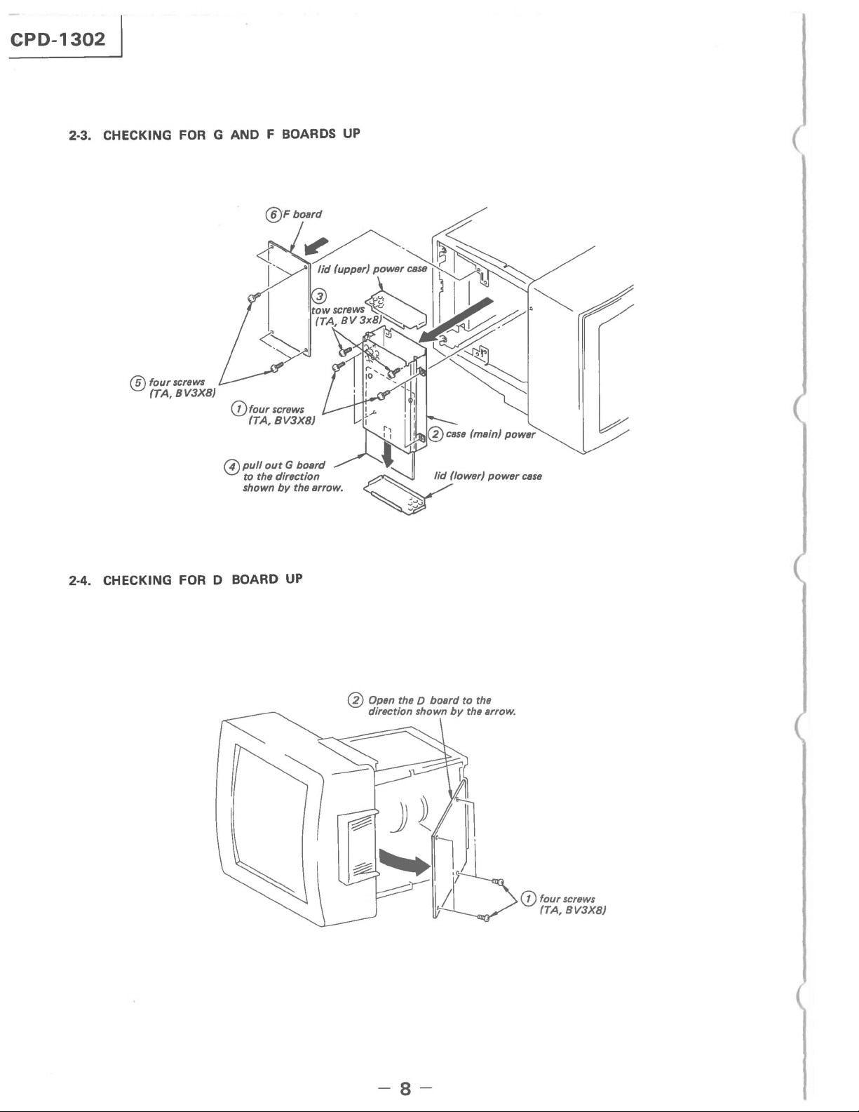
2·3. CHECKING
®
four
(TA,
FOR
G AND F BOARDS
screws
BV3XB)
(])
@
pull
to
shown
four
screws
(TA, BV3XB)
out
G boerd
the direction
by
the errow.
UP
2·4. CHECKING FOR D BOARD
UP
® Open the D
direction shown
boerd
by
to
the
the arrow.
-8-
CPD-1302
CPD-1302
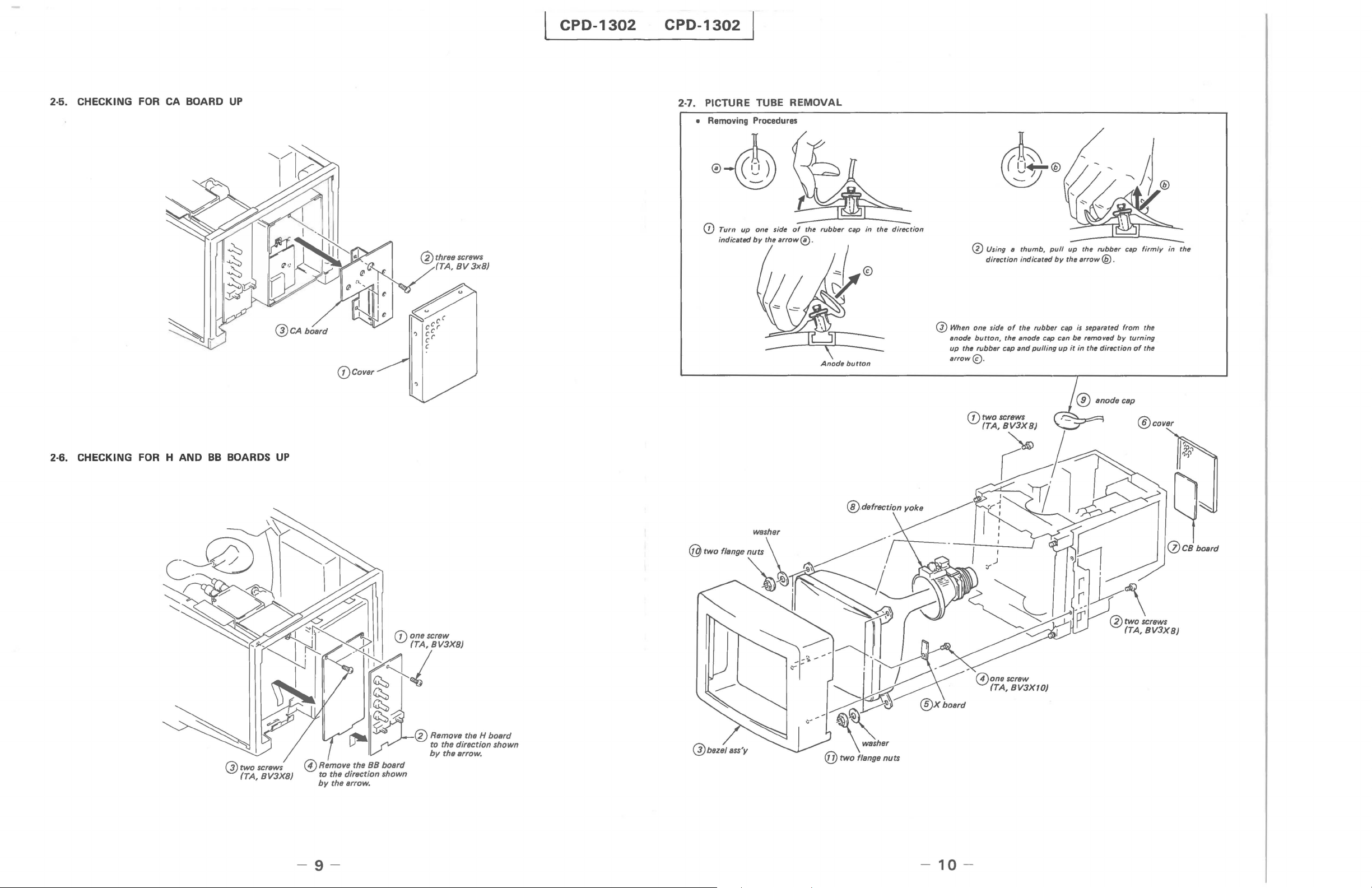
2·5. CHECKING
FOR
CA
BOARD
UP
@CAboard
(j)Cover
2·7. PICTURE TUBE REMOVAL
• Removing Procedures
CD
Turn
up
one
side
of
the
indicated
by
the
arrow
rubber
0.
Anode
cap
button
in
the
direction
o When
anode
up
arrow(£).
o Using
one
button,
the rubbtJr cap
IJ
thumb,
pull
direction
indicated
side
of
the
rubber
the anode cap can be removed
and
pulling
by
thelJrrow
cap
up
up
it
is
in the
the
rubber
®.
separated
direction
by
cap
from
turning
of
firmly
the
the
in
the
@cover
2·6. CHECKING
FOR
HAND
BB
BOARDS
@twoscrews
(TA, BV3XB)
UP
I
EJ;-\
~
@
two
screws
(TA,
BV3XB)
-9-
-
10-
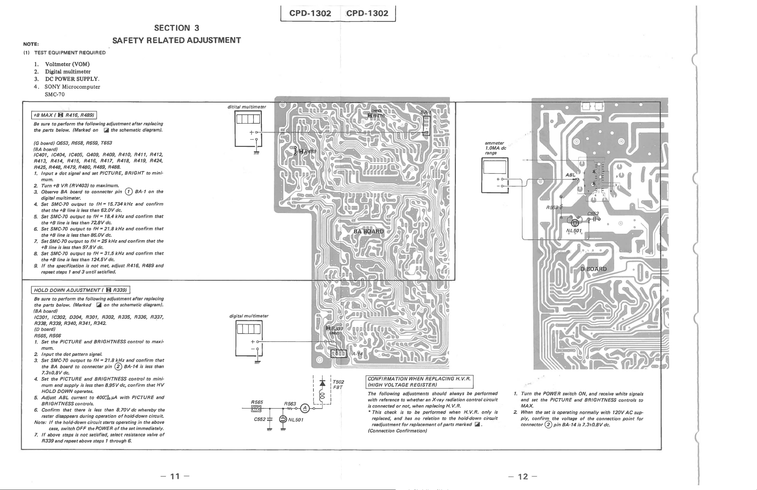
SECTION 3
CPD-1302
CPD-1302
NOTE:
(1)
TEST EQUIPMENT REQUIRED
1.
Yoltmeter (YOM)
SAFETY RELATED ADJUSTMENT
2. Digital multimeter
3.
DC
POWER SUPPLY.
4.
SONY Microcomputer
SMC-70
I +B
MAx
( 8 R416, R489) I
Be
sure
to
the parts below. (Marked on
(G board)
(BA board)
IC401, IC404, IC405,
R413, R414, R415, R416, R417, R418, R419, R424,
R425, R448, R479, R480, R489,
1.
2.
3.
4.
5.
6.
7.
B.
9.
perform
0653,
Input a dot
mum.
Turn +B VR
Observe BA board
digital
multimeter.
Set SMC-70
that
the +B line
Set SMC-70
the +B line
Set SMC-70
the +B line
Set SMC-70
+B line is
Set SMC-70
the +B line is
If
the specification is
repeat steps 1
the
following
R658, R659, T653
0409,
signal
and
(RV403)
output
output
is
less
output
is
less
output
less
than
output
less
and 3 until
is
to
less
than
than
to
97.8
than
to
connecter
to
than
to
728V
to
86.0V
fH
to
124.5V
not
adiustment
~
the schematic diagram).
R409, R410,
R488.
set PICTURE,
maximum.
pin
fH
= 15.734
62.0V
fH
fH
V
fH
dc.
= 18.4
kHz
dc.
-
21.8
kHz
dc.
'"
25
kHz
31.5
dc_
and
kHz
dc.
=
met, adiust R416,
satisfied.
after
R4",
BRIGHT
CD
BA-1
kHz
and
and
confirm
and
confirm
confirm
and
confirm
replacing
R412,
to
mini-
on
confirm
that
that
that
that
R489
and
ammeter
1.0MA dc
the
the
I HOLO DOWN
Be
sure
the parts below. (Marked
(BA board)
IC301, IC302, D304, R301, R302, R335, R336, R337,
R338, R339, R340, R341,
(D board)
R565,
1.
Set the
mum.
2·
Input
3_
Set SMC-70
the
7.3±0.8V
4.
Set the
mum
HOLD
5.
Adiust
BRIGHTNESS
6.
Confirm
raster disappears during operation
Note:
7.
If
above steps
R339
ADJUSTMENT
to
R566
the
BA
and
DOWN
If
the
case,
and
perform
ABL
the
following
PICTURE
dot
board
dc_
PICTURE
supply
that
hold·down
switch
repeat above steps 1 through
and
pattern signal.
output
to
to connecter
and
is
less
operates.
current
to
controls.
there
is
circuit
OFF
the POWER
is
not
satisfied, select resistance valve
( B R339) I
adiustment
~
on
the schematic diagram).
R342.
BRIGHTNESS
fH
=
21.8
pin 0 BA-14
BRIGHTNESS
than
8.95
400~fojJA
less
than
starts operating in the above
after
control
kHz
and
confirm
is
control
V dc,
confirm
with
PICTURE
8.70
V dc whereby the
of
hold-down
of
the set immediately.
6.
replacing
to maxi-
less
to
that
circuit
that
than
mini-
HV
and
of
digital
multimeter
III
Ii
}o-:-J
--~e.N
~~~~~~
I
: T502
I
FBT
I
CONFIRMATION
(HIGH
VOL
The
following
with reference to whether an-X-ray radiation
is
connected
• This check
replaced,
readiustment
(Connection Confirmation)
WHEN
TAGE
adiustments should always be
or
not, when replacing
is
and
has
for
REPLACING
REGISTER)
to
be
performed
no
relation to the hold-down
replacement
H.
H.
V.
R.
when
of
parts marked
V.R.
control
H.
performed
circuit
V.R.
only
circuit
~.
1.
Turn the POWER switch ON,
the set
confirm
PICTURE
is
operating
the voltage
pin
BA-14
and set the
MAX.
is
2
When
ply,
connector 0
and
receive white signals
and
BRIGHTNESS controls
normally
of
is
with
the connection
7.
3±0. 8 V
dc.
120V
AC
point
to
sup-
for
-
11
-
-
12-
CPD-1302
CPD-1302
.·.·.HT
"
...•
....
.
'.5IIFT
"fT~
~r
'zoo
---
j
,.w
..
-
"
l
.YO
v.-·
I
,.w
-
..
.~
,IT
51
....
t
F
f
~
;l
til
---~
n.
.J;J.,
~
.~'~
~
,------
.......
,
""'IUI
I 11,,'8
01lL,RI,'ll
'-------
... -.... --..
---------
r-----~~~
Tr-'
'ItO'T!CT
••
~r_----------+---+-----+-~~
.....
,
11£1
'[f>l101£Cl
030)1
,300Z
J:~:!~'~'~
CA
CUT
I-·"J·";}·'-~'~·'=·'~i--------------------------""'~!;!;!~----""---~!...~------~!:!..-'
I I
.-
rocus
________________________________
1 i
J<-"
..
t---------------~.
1
-----1~-------
,<4"
...
rCCTM.
I
~
r-
-!,
,
R·'
..
--------------------------~------~
!
jI---
I
LOIIC
~tLST"'T
CB
•
·'
9
It·'·a
GO
..
1
".,
.,
CAM"'
C
~"u
V901
PtCTURt:
TUBE
H.'
COO,
WDCOIiIT
~
P2.
<.".
.
..
r-----------
iIZVIIU
1<'"
Ok'
'.'"
...
,
V.ILK
....
~~
r--1----------------------------------------------------,
HQ~:
1-----------.01;
-
-----------
.~!
""
~-"jft<.I!i-----------l
H.M
""
"'.'"
-
------------.
D
r,I.T
l-------;
t \ :
,:±:
H~·
L
_______
~4-
TOOl
r-=-.-~
H.V
.R
-'l'
I~
g
t"'
.J
,
I
..
~~''---rt-H~~4-f---~--~
t-t------t--t-------1--t-+---1--t-+--+---+------I---+----~---r:;r]~=":"=--~
H.DRlYEII\FF
042.1
v.,
....
, .
......
---------L4r~.",~~~~-
t~
----------r-,---------+----l-~-~~:j~t__rr-----t-II---------r-t-----l-----t~~-t-+--~t--------+------
~
uy---w;u-
.....r::-~
~r_------------~-------J--t+-----+------,
....
-
"'lAC
1
-
-----------------------------+4--~41---------------------------------------------------------~
__________________
O4G1
~
~
I
~
H.v.lurF
-1
________
r
~
~
m-
~
,-
~n'
~
~
~
____________________________
--1
.:;':.
j,I:mol
1,
1----.1
~~
iL.!!!LJ T
~CIWill
·--L..!!!LJ---U~104
======================================================~
t-
________
'.F'"
OW
301
U
I.~
~
+-
______
__
-+
______
)O'J
lO~
cf'F-I
T
Q)OI~
+12V
~------~-+--~-H.OW~~~'
L_"_'_'
____
~-------+--~----------~======~f'
_~
IC405
~~--~~~
FNCON'
I
.,
V,IN
V.NF
~
"
~
'"''
),-
....
"
....
'TIll.
,
•
t>-
, ,
~
./
,
~
YIAI1HIliAI
1
UTt+I
.'"
M"lI3lJOIT
,
=::=
.,
•
I
...
IHSW
",
ow
,
..
0513,5.l4
~
T
'tNOIT
''''
,0'
~
+IZV
r----~
rrn
r---i
.""
LllI
u.
-~
I
______________________
~_=_=_=_=_=_=_=_=_=_=_=_=_=-_-~-=_=_=_=_=_=_=_=_=_=_=_=_=_=_=_=_=1H~.a~
... 1 J
1
O:,sot.~
11--...,----I-----I-----4---------------------~--!!,H·!!"--~~---!_---~'i
~
.,,"
,
...
..
--------------I
'."'
, I
H.Of c;JL
'----
15
16
-
-

CPD-1302
CPD-1302
11
,--(10
HVIi
12
13
14
!
15
I
16
17
18
19
20
o
....
21
B
VIDEO,IF,INT
B(
R·G·B
OUT
22
SW.)
.
23
24
25
26
27
•
IC405
HOI453a8P
~
88-3
~
$~
"'"
~"
___ -I ...
0412,414
IlH]iiJ j " ), •
0413
2SC2785
!!iillJ
0407
25AI175
CillimJ
2~~5
~
WI
LlJ
"
258740
0415
2SC2785
mimi
0321
2SC2785 2SC2785
~
0323,324
25C2785
(ilftfiliI
0322
[illIDj]
I
"~
~
..
~
" "
~
~
! !
...
, ,
.
1"
BA-II
:h:,
.
.:;2J.
i%
••
0-10/"
~~'
~
,::>\I
.'.
\rN...
-F-«;
..
" 1
I,
J..
~
m,
"'''
!I'M
~
-
fM
1
a
0403
ROIOEL3
~
... , IC404
_CX22030
~
0425,426
2St2ZB5
~
0428
?
TCI2$4
I
He
,427
~ 5
w
..
"
...
..
,.
..
j
..
n
J.'h
0
~
5
0424
~
'I.a
~
•
i
2SC2785
04
16
25C2785
~
IC403
MC1451sBC!'
~
033~175
0334 25A
I175
IMUil
01
01
155119
~
01
02 155119
[mfJ
O\o~1I
9
0104 155119
~
0~1I9
~
1I9
0119
2SC4035P
IiR"fE
0120
2S~P
[!H!1j]
0116
25C4035P
~
..
ICI05
0117
2SC4035P 0119 2SC4035P
[!Q!l
5N74515N
~
'I
~ T
sO',
~~~~~~~~
l
01
15 ":
25C4035P
~
L-
___________________
I
ml
~
,
J:~
l
~
~~~~~'~2~
1»
-.' ..
f.t'l....
.- _
.,,' '-..C.+ "M
II""
~~'='
____
~.~~
..
I •.
,~",'
~
0
'IJ
~'Q'
n
,g,"
'j
" ...
'"
ICI06
'
~
'
l!
'
J
'
~
';:;
'
~
_______________
74FI38PC
__
~
-
19
--
--
20
--
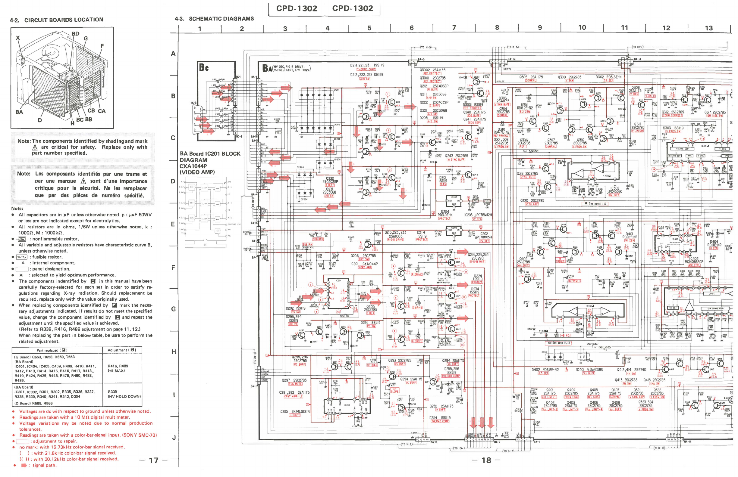
4·2. CIRCUIT BOARDS LOCATION
Note: The components identified by shading and mark
&.
are critical for safety. Replace only with
part number specified.
Note:
Les
composants identifi6s par une trame
par une marque
critique pour
Que
par des pieces
&.
la
s6curit6.
$Ont
d'une
Ne
de
num6ro sp6cifi6.
importance
les remplacer
..
:~::
et
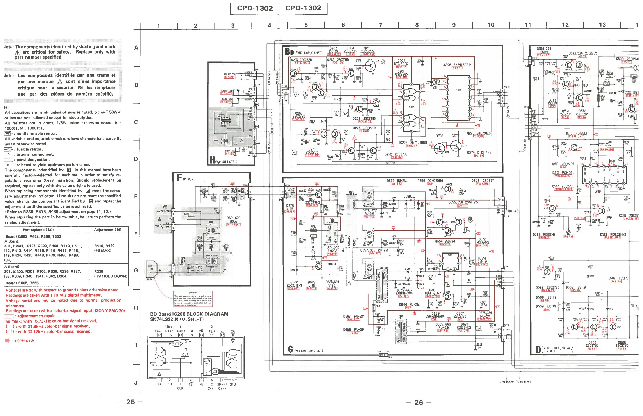
4·3. SCHEMATIC DIAGRAMS
1
2
A
Bc
t -I
,~
" .
~
B
c
1It
--f-l.-
~
~
O--t
~
-r , ....
"O"
lra
_ '
""
;t
! '
1
_. ___
BA Board IC201 BLOCK
DIAGRAM
CXA1044P
(VIDEO
AMP)
o
[~
"
'"
. ,
';7,;
~~,41JN
ti
L90'~
"'~~
~
W'
[
901 0.41;1
' W '
.....
V
I
.
l I
I
BC
2
•
BA
SA
-
. ;
'V
~
,~'
...
':
'
CPD-1302
3
HV
OSC
, R
·G·B DRIVE
~
'1
l L_ _
. )
1.--
V.
FREQ CTRT, F/V CDNV
(
-,0
II
l
'JJ8'
.
CPD-1302
4
--
- I-tl-
-
I-~
5
6
7
8
9
10
11
12
13
I
9A
' 3
BA-12
r=
~
eA-1<
0:
Note:
•
All
capacitors are in
or
less are
not
•
All
resistors ara in
1000n,
M :
1000kn.
•
-m-
: nonflammable resitor.
•
All
variable
unless otherwise
•
~
• t;. : internal
•
c:::::J
•
lIE
•
The
carefully factory-selected for each
gulations regarding X·ray radiation. Should replacement be
requirad ,
• When replacing
sary adjustments indicated.
value, change
adjustmant
(Refer
When
related
(G
Boardl
(BA Boardl
IC401, IC404. IC405,
R412,
R413
R419.R424,
R489.
(BA Boardl
IC301, ICJ02 , R301,
RJJ8,RJJ9,
(0
Board) R56S, R566
• Voltages are dc with respect
• Readings are
• Voltage
tolerances.
• Readings are taken with a color-bar-signal input. (SONY SMC-70)
•
• no mark: with
(
((
))
•
..
and
: fusible resitor.
: panel designation.
: salected
components
replace
until
to
R339, R416, R489
replacing
adjustment
Part replaced (
0653
. R658 . R669.
, R414, R415, R416, R417, R418 ..
R42S, R448,
R340,
variations my be noted
:
adjustment
):
with
21.8kHz
: with
30.12kHz
: signal path.
pF
indicated
adjustable resistors have characteristic curve
component
to
componants
the
the
0409,
RJ02,
RJ41,RJ42,D304
taken
15.73kHz
unless otherwise
except
for electrolytics.
ohms,
1/6W unless otherwise noted. k :
noted
.
.
yield
optimum
indentified
only
with
component
the
specified value
part
.
I.iiII
T653
R409, R410, R411,
R479,R480,
R33S,
with a
to
repair.
color-bar signal received.
color·bar signal received.
performance.
by
the
value originally used.
identified by
If
results
identified
adjustment
in below table,
R488,
R336, RJ37
to
ground unless otherwise
10
Mn
color-bar signal received.
noted.
p :
ppF
B in this manual have been
set
in
order
to
[;iii
do
is
achieved.
,
digital multimeter.
due
mark
not
meet
by
B and repeat
on
page 11, 12.)
be
usre
to
Adiustment ( B I
R416, R4B9
(+B
MAXI
RJ39
(HV HOLD
to
normal
the
perform
DOWNI
production
50WV
satisfy
the
neces-
specified
noted.
-
B,
reo
the
the
17
E
F
G
..
n
.,
.
'-
H
OA' 17
~
I
C205
SN74LS22)N
!iilliITJ
J
'--
-----
- - -
-----
-
---------,:-<
10
H-~
-
BA-
I!i
(
TO
CA' ) ) ) ) ) ) ) ) )
\
-
18
BA
-9
C""'(ro
-
H}-
:......J
o I
BA
-I
D-
BA-II
CPD-1302
CPD-1302
I
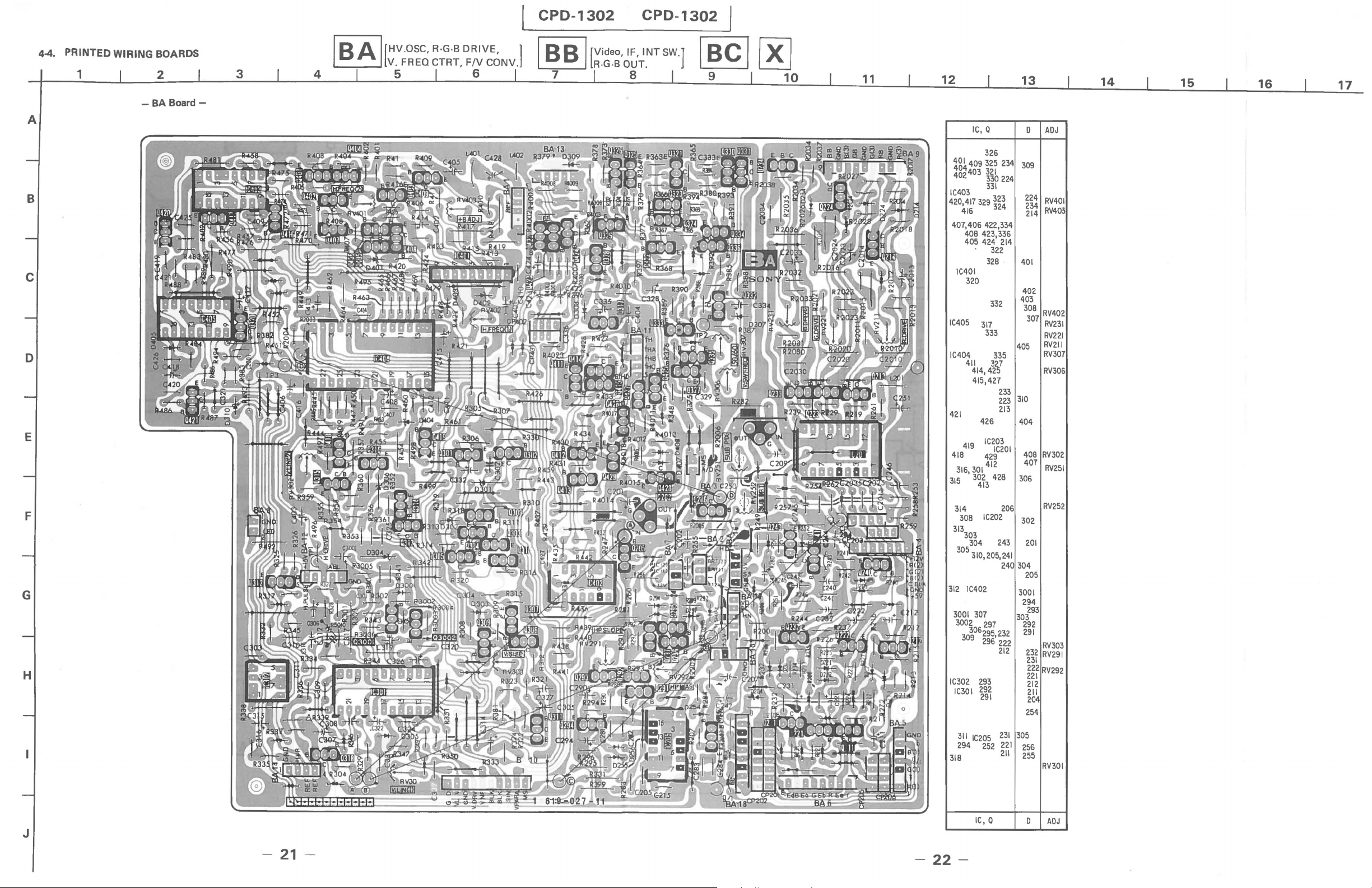
4-4. PRINTED WIRING BOARDS
1
2
- BA
A
B
c
o
E
Board-
3
I B A I [HV.OSC, R·G·B DRIVE, ]
V. FREQ CTRT,
4 5 6
F/V
CONV.
I B B I [VideO, IF, INT
R·G·B
7 8
OUT.
SW'J
11
12
IC.
326
40 I 409
325
404
403
402
IC403
420.417329
416
407.406422.334
408
423.336
405
424
lC401
320
IC405
317
333
IC404
411
414.42
415.427
421
426
IC203
419
418
429
412
316.301
315
302
413
Q
234
321
330224
331
323
324
214
322
328
332
335
3~7
233
223
213
IC201
428
13
309
401
402
403
405
310
404
306
0
224
234
214
308
307
408
407
ADJ
RV401
RV403
RV402
RV231
RV221
RV211
RV307
RV306
RV302
RV251
14
15
16
17
F
G
H
J
314
IC202
308
313
303
304
305310.205.241
312
lC402
3001
307
3002
297
306
309
295.232
296
IC302
293
292
IC301
291
311
IC205
294
252
318
IC.
Q
206
243
240
222
212
231
221
211
302
304
3001
294
303
292
291
305
256
255
201
205
293
232
231
222
221
212
211
204
254
D
RV252
RV303
RV291
RV292
RV301
ADJ
- 21 -
-
22-

CPD·1302 CPD·1302
15
16
17
- BB
18
Board-
19
20
21
22
23
24
25
26
27
28
29
30
-
Be
Board-
- X
Board-
1·619·036·
X
SONY
11
\\~~
.....
~L..U~d'
-
23-
-
24-
/

CPD-1302
CPD-1302
11
----
--------------------------------------------------------------------------------------------~goB~11r-~,,~
12
051
6
~
2785
I
ltElABM'iI~rrf
I
L
13
14
15
16
17
18
19
20
0504,505,516
~
21
22
23
II~
Ml
. 330,
12
. ,
000
05003
~
"
VIIN
C!IOQ2
2t!v
24
25
CalCRT
'
'--''''
A
SOCKET!
II
26
27
..
"I
...
L
;4-
I
05
U
0509
D(
5119
155119
[S]]!I
V'H' C B
H.V
OUT
05
01
O
TCI
24E5
0518 25C2785
Iv
PULSE
sw
l
IIIDl
....
'"
+ C
!l4.l!
~
Ai:
.."
'"
000'
.
50<
~~
----~------r_----_+----------------------------_+r_----_+_+_r~~--
¥I""-
-~
~
DS09
I
Ooo,
~
""
LK.f
H S
W.)
.
..I.
0507
IlHUiBJ
0518
15511
9
0518
15511
9
~
~~aoo~33
f~
r-J~~'~
-.
\~~f.
..
.
""
!
IMW
~515
2
~
I
IOOV
too
v
100
A!i47
1t549
33k
lOO
k
,I/eWI
--------------tt----------
11
11/4 ...
1
i:t.f
IH.~tl
l
SI
oa.
05
10
2
501134
Ifj[]jl!J
I 2 ,
- 0-8
I
~
05001
1525~!J~
IV
~
~
=++=4=::::::::::::::::
~
a
0-3
~
::::::::::~
~
.,
-0
-4
fI
~::
~
""
::::::::::::
"0'
+I
""
120
...
;::-"
J"
1
5011
0-2
~
~t=
0513
FMU-265
~
0514
VI9G
([IQY]ill]
::::::::::::~tt1
0-5
,-{TO
BA-
I
..
.,
III ,
.2
GIll .
'
f-\:J-
D-6
0-7
'1",
Ir
'
~
---
<lOV
072
\G
~~~
2688
0731
CAIR
25C2688
IDYIl
.G'B
OUT!
mT!:l
IFOCUS
\I~
RV1Q
l
...
.
.J
BA
BOARD
--
27
--
--
28
--
CPD-1302
CPD-1302
Jote: The
~ote:
te:
All
or
All
1000n,
components
& are critical
part
number
Les composants identifi6s
par
une
critique
Que
par
capacitors ara
less
are
not
indicated except for electrolytics.
resistors ara in ohms, 1/6W unlass otherwise noted. k :
M :
1000kn.
identified by shading and mark
for
safety. Replace only with
specified.
par
marque
pour
des pieces
in
&
sont
d'une
la
s6curit6.
JJF
unless otherwisa noted. p :
Ne
de
num6ro sp6cifi6.
une
trame
et
importance
les remplacer
JJJJF
50WV
m-: nonflammable rasitor.
All
variable and adjustable resistors have characteristic curve
unless otherwise notad.
~:
fusible resitor.
A : internal component.
~
: panel designation.
lit : selected
The components indantified by
carefully factory-selectee;! for aach
gulations regarding X-ray radiation. Should replacement be
required, replace
When replacing components identified by
sary adjustments indicated.
value, change the
adjustmant until
(Refer
When replacing
related adjustment.
Board)
A Board)
401.
IC404. IC405,
J12, R413. R414, R415, R416, R417, R418,.
119, R424, R425, R448, R479, R480, R488,
189.
A Board)
301,IC302,
138,
R339, R340, R341, R342,
Board) R565, R566
Voltages are dc with respect
Readings are taken with a
Voltage variations my
tolerances.
Readings are taken with a color-bar-signal input. (SONY
----=:J
: adjustment
no mark: with 15.73kHz color-bar
(
I:
((
II
: with 3O.12kHz color-bar signal received.
• : signal path
to
yield
optimum
only with
component
the
to
R339, R416, R489 adjustment
Part replaced 1 ~ ) Adjustment 1 8 )
0653,
R301, R302, R335, R336, R337, R339
with 21.8kHz color-bar signal received.
specified value
the
part
R658. R659.
0409.
to
repair.
R409. R410. R411,
performance.
B in this manual have been
sat
in
order
the
value originally used.
If
results
identified by
in
below table, be usre
T653
0304
to
ground unless otherwise noted.
10
Mn
be noted due
digital multimeter.
signal received.
[;i
do
not
meet
IB
is
achieved.
on
page 11,
to
normal production
mark
to
satisfy re-
the
the
specified
and repeat
12.1
to
perform
R416. R489
1+8
MAX)
IHV
HOLD
SMC-701
neces-
the
the
DOWN)
B,
:::
1
A
B
c
D
E
' W ' W
SlOt
F
.--
I "
=-
G
~
~
~
H
BD
Board IC206 BLOCK DIAGRAM
SN74LS221N
v~
-l16~
~-I
I
+--
4
~
ow,
.. ,
1"-1
~
T
TlIHO'
2
r-'!l
'102
.".
!tOWI
3
RV1
a03~~
~
0601,602
U05E
~
N.~
L...l....-J
'"
.r
Me
ac
~
.
!I..re
Ae
~
I
~
I"-'''
~
-
''.
-
'''
-
_
-
;'::
_
..............
the DIIII1'I When '
blJU
....
~il
blfaw-nlnthildi
(V. SHIFT)
I R. x t I
cg,t
~t
-lIS!.
-l14,
--1131.
~
I~
1!'J!\
~
-
:'
-
:'~
-
''''
,,"
....
1CinI
..
'thSPK,f,.cIpar111U11'1
...
_
~
~~
L
__
r~
&
-
';'''
-
K
-
_
-----''''''
......
;
.....
,,""
the
Ie
_ cord
2
AjH{~JL
G I
Vee
CRTL,REG
5
OUT!
0203
~
6
0264
2
nEm
0667
I1EDilll
0668
GKJ!illJ
5
~
RU-2M
RU-2M
0261
~
7
8
1C206
9
5~7A15221N
1
v H
0274
OTCII4E5
Ipc
swl
10
..
"'"
:
y" ,
BD-2
L
-r
P<ro
G-3
G-4
1
BA-I
}
11
0531,532
J
"y
.•
"
~
,,.,
""
D-12
~I'f
<OIItV
y.
y.
IV.PAL
'is
D(
'ffl
J~JI
~
C557
+ 0531
22
'"
lrH~~
E
V'H'C
BLK.fH
H.V
OUT.
12
0533,534
'
'
~'
~~
mil
row·4H
"31
.~
D$3l rr""'\. '-2
I'
''.",
''''''10.7"
1
10k 10.
10.1
053
1
0532
5
21
iW,;1
0'"
SW,)
""'"
I
".
13
25C2785
m
I~
0
533
101
~~
10.
5
""
'"
"""
0509
25C2785
Illl::lll
~
-
R
~
:n
0507
"HB
05l!
~
155119
PINI
..
..
'0
'
L _ZSlli
0518
1
[l
!
25
~
~========~~===========
J
I
...
IB
CLR
III
2!l
Caxt
2Rn t tlND
t
Cax
-
26
-
l~
T
TO
BB
BOARO
TO
~~~~~~
BA
BOARD

A
B
- 0
1
Board-
2
3
4
V.H.C
BlK,
fH
[
H.V OUT.
SW,]
5 6
CPD-1302
[V, H
SIFT
CRTL.]
7 8
CPD-1302
CRTl,
[Vee
9
REG
OUT]
10
[CRT SOCKET]
11
IC,O
0
5001
5001
511
512
5002
516
505
504
IC505
ADJ
I B D I [SYNC AMP, V SHIFT.]
12 13
- H
Board-
14
[IJ
[POWER]
15
I C A I [R.G.B OUT]
16
- G
Board-
"
17
c
D
E
G
H
F
514
513
507
506
519
IC504
521
502
520
IC501
501
532
534
503
533
518
531
515
516
522
509
508
5fo
517
514
5003
510
536506
512,507
513
526
51\
529
523
525
524
515
535
534
528
533
m
517
509
508
518
522
RV506
RV503
RV505
RV570
RV504
RV580
RV502
I·
loci·
I· I !I·I·I·:I·I·I·I·I
- F
"
Board-
IC,O
0
ADJ
J
-
29-
-
30
-

CPD·1302
CPD-1302
[f]
I
[POWER]
15
leA]
I
[R.G.BOUT]
16
- G
Board-
o
I
17
18
19
20
21
22 23
24
25 26
-
CB
Board-
27
28
-BD
Board-
29
30
31
- F
@
o
Board-
1-619'034'11
o
- CA Board - '-======:=--1
- 31 - -
32-
CPD-1302 CPD-1302
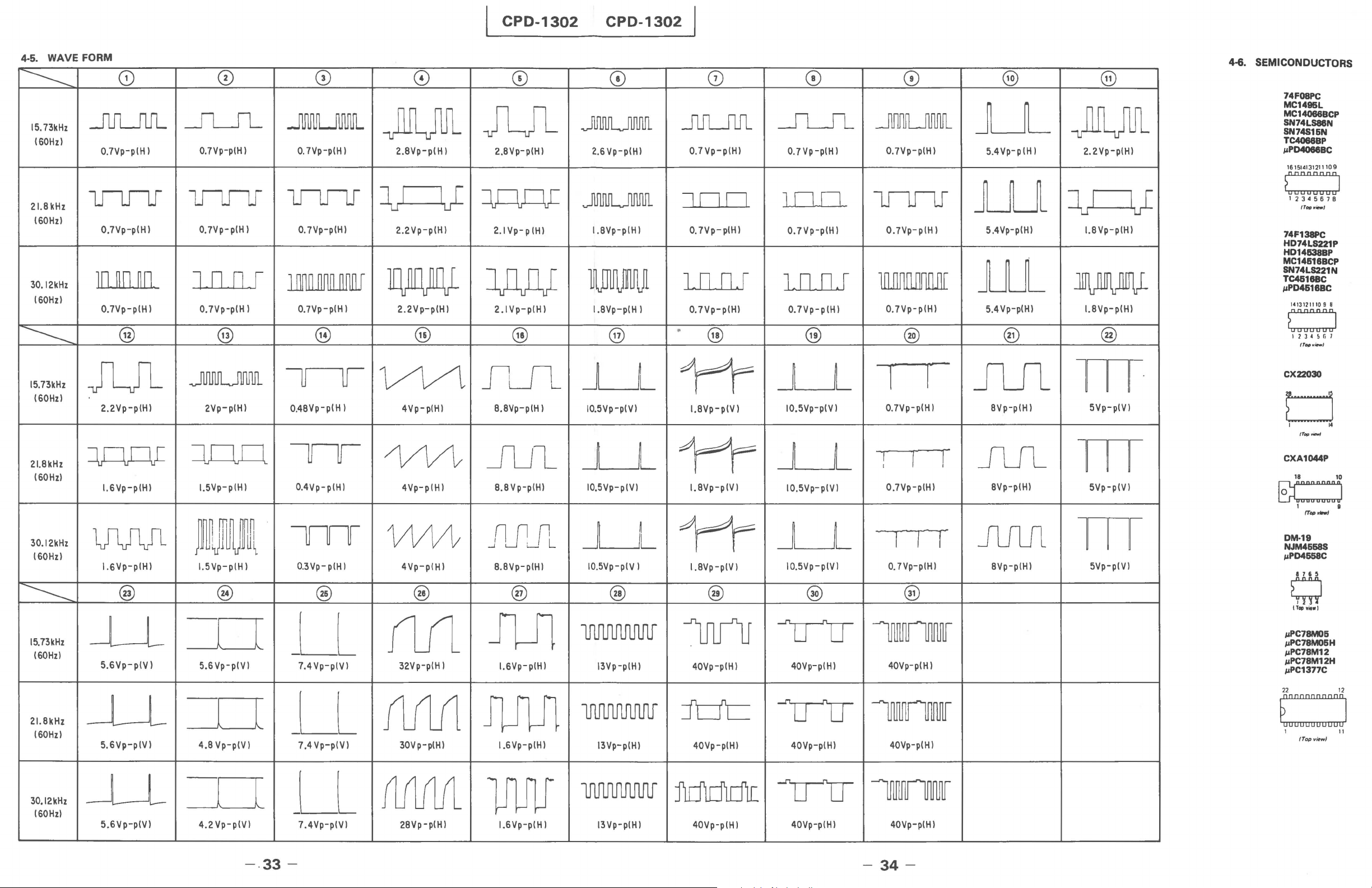
4·5. WAVE FORM
-----
15.73kHz
160HzI
21.BkHz
160HzI
30.12kHz
160HzI
-----
15.73kHz
160HzI
JlJL.JlJL
O.7Vp-pIH I
In.rlJ
O.7Vp-pIH I O.7Vp-pIH I O.7Vp-pIHI
JO
O.7Vp-pIH I O.7Vp-pIH I
JUl
2.2Vp-pIHI
(0
~O
~O
@
CD
---1LJL
O.7Vp-pIH I
In.rlJ
] n n
@
Jlf1JlJUlI1J1Il
2Vp-pIHI
I
0
JlJWUlMIl..
O.
7Vp-p1H I
In.rlJ
ll1l1ilJlJ1ILil
O.7Vp-pIH I
@
uu
O.4BVp-pIH I
JRjlSL
2.BVp-pIH
~I
2.2Vp-pIHI
1llrllDJlDJ-
2.2Vp-pIHI
VV1
0
@
4Vp-pIHI
I
IJ
0
JUl
2.BVp-pIHI
mAC
2.IVp-pIHI
JJlA[
2.IVp-pIHI
@ @
J'ul_
B.BVp-pIH I
0
JliULJlJlJ1fl
2.6Vp-pIHI
JlflJliLJlflJli
I.BVp-pIHI
\illIUlliUl
I.BVp-pl
J
IO.5Vp-pIVI
HI
fL
0)
JlJLJ1fL
O.7Vp-pIHI
JOD
O.
7Vp-
plH
I
In
•
n.!
O.7Vp-pIHI
@
tt
I.BVp-pIV
I
0
J1.Jl..
0.7
Vp
-plH
JOO
O.7Vp-pIHI
In
n.!
O.7Vp-pIHI
@
~
IO.5Vp-pIVI
4-6.
SEMICONDUCTORS
0
-.flIl.nu.
I
O.7Vp-pIHI
lJ1JlJ
O.7Vp-pIH I
1illlI1lliJf1Il
O.7Vp-pIHI
@
r
O.7Vp-pIHI
I
@
LL
5.4Vp-pIH I
JUU
5.4Vp-pIHI
ill
5.4Vp-pIHI
@
JUl
BVp-pIH I
@
JRjlSL
2.2Vp-pIHI
1u
I.BVp-pIHI
1
IJ
JlllJlITVill1l
I.BVp-pIHI
@
m·
5Vp-pIVI
74
FOSPC
MC1496L
MC14066BCP
SN74LS88N
SN74S16N
TC4066BP
I'PD4088BC
161514131211
~::::::::I
12345678
74F138PC
HD74LS221P
HD14638BP
MC14618BCP
SN74LS221N
TC4618BC
I'PD4618BC
14131711
(::::::1
I 7 3 4
CX22030
t=J
I
".";"'/
(TOIl"'"
(Top .".""
109
~
r.
109
8
1
14
21.BkHz
160HzI
30.12kHz
160HzI
mAC
lJlJlJL
-----
15.73kHz
160HzI
21.BkHz
160HzI
-Ll
5.6Vp-pIVI
-Ll
5.6Vp-pIVI
JDD
1.6Vp-pIHI
1.6Vp-pIHI
@ @
~
~
~1lJ
1.5Vp-p
IH
I
J{J~~~l
1.5Vp-p1H I
L
5.6Vp-pIVI
L
4.B
Vp-pIVI
O.4Vp-pIHI
!ITT
O.3Vp-pIH I
@
LL
7.4Vp-pIV\
_U
7.4Vp-pIVI
/\/Vv
4Vp-pIHI
WIt
4Vp-pIHI
@
M
32Vp-p1H I
JlJ1J1
30Vp-pIHI
JlJL
B.BVp-pIHI IO.5Vp-pIVI
JlJlJL
B.BVp-pIHI
@ @
J
J
IO.5Vp-pIV I
lJUlIVlf1SlJlf
JUl
1.6Vp-pIHI 13Vp-pIHI
lJUlIVlf1SlJlf
IWl11
1.6Vp-pIHI
13Vp-pIHI 40Vp-pIHI 40Vp-pIHI
fL
!
IL
1=r
I.8Vp-pIVI
tt
I.BVp-pIVI
@
1JUlJ
40Vp-pIHI
fdt=
1
~
IO.5Vp-pIVI
~
IO.5Vp-pIVI O.7Vp-pIHI BVp-pIHI
@
Utr
40Vp-pIHI
Utr
I
O.7Vp-pIHI
1 I
@
lIlrlflrr
40Vp-pIHI
lIlrlflrr
40Vp-pIHI
I
I
I
-
1
JlJL
BVp-pIHI
JUU1
m
5Vp-pIVI
m
5Vp-pIVI
CXA1044P
18
~:::::::]
1
DM·19
NJM4668S
I'PD4&58C
• 7 ,
Q
t
Tap
$lPC78MO&
I'PC78M05H
I'PC78M12
I'PC78M12H
I'PC1377C
22
~::::::::::I
I
(Top viewl
"
.,,1
...
-/
~
10
8
12
II
30.12kHz
160HzI
-Ll
5.6Vp-pIVI
~
4.2Vp-pIVI
L
-·33
_U
7.4Vp-pIVI
- -
J1flflfL
2BVp-pIHI
lJUlJ
1.6Vp-p1H I 13Vp-pIHI
lJUlIVlf1SlJlf
fldldLdk
40Vp-pIHI
Utr
40Vp-pIHI 40Vp-pIHI
lIlrlflrr
34-
CPD-1302
CPD-1302
v
Jill-
.
-pIHI
=v
-pIHI
VillU-
-pIHI
~
T·
-pIVI
T
'pIVI
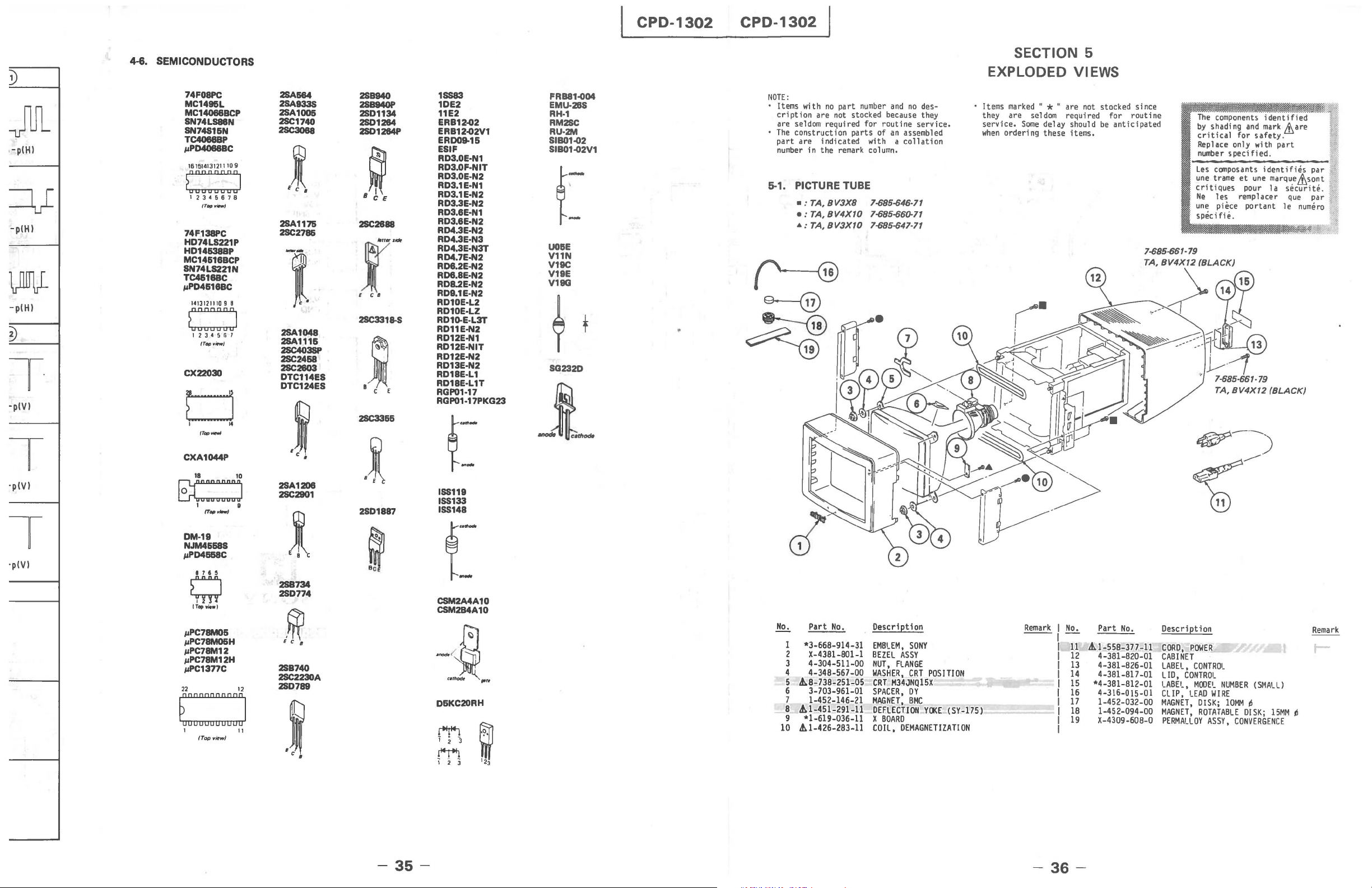
4-8. SEMICONDUCTORS
74FOSPC
MC1495L
MC14066BCP 2SA1006
8N74LS88N
SN74S16N
TC4088BP
"PD4066BC
161514131211109
~::::::::I
12345678
ITop,,;""'1
74F138PC
HD74L8221P
HD14638BP
MC14618BCP
8N74LS221N
TC4618BC
"PD4&18BC
1413121110 9 8
~:::::::I
1 2 3 4 S
r.
7
(Top
11ft}
CX22030
t=J
1
CXA1044P
18
8J:::::::]
(rep
I
rr.,._J
WftW
14
10
g
2SA1584
2SA933S
2SC174O
2SC3088
.f
2SA1176
2SC2786
--
f
2SA1048
2SA1116
2SC403SP
2SC2468
2SC2803
DTC114E8
DTC124ES
.i
•
28A1208
2SC2901
28B940
28B94OP
28D1134
2801284
2801284P
~
BeE
2SC2888
r-
E
C.
2SC3318-S
~
B C £
2SC336&
1SS83
1DE2
11E2
ERB12~2
ERB12~2V1
ERD09-16
E81F
RD3.0E·N1
RD3.0F·NIT
RD3.0E·N2
RD3.1E·N1
RD3.1E·N2
RD3.3E·N2
RD3.8E·N1
RD3.8E·N2
RD4.3E·N2
RD4.3E·N3
RD4.3E·N3T
RD4.7E·N2
RD8.2E·N2
RD8.8E·N2
RD8.2E·N2
RD9.1E·N2
RD10E·L2
RD10E·LZ
RD1G-E·L3T
RD11E·N2
RD12E·N1
RD12E·NIT
RD12E·N2
RD13E·N2
RD18E·L1
RD18E·L1T
RGP01·17
RGP01·17PKG23
~-
.~
..-
ISS119
ISS133
28D1887
ISS148
FRB81~04
EMU-28S
RH·1
RM2SC
RU-2M
81B01~2
SIB01~2V1
i~
U06E
V11N
V19C
V19E
V19G
f
~
80232D
1-
NOTE:
Items
with
no
part
cription are
are
seldom
The
part are indicated
number
5-1. PICTURE TUBE
required for routine service.
construction parts of
in
the
.:
TA,
: TA,
•
.:
TA,
not
stocked
remark
BV3X8
BV4XtO
BV3XtO
number
and
no
because
an
with
column.
7-685-646·71
7-685-660-71
7-685-647·71
assembled
a collation
desthey
SECTION 5
EXPLODED
•
Items
marked" * " are
they are
service.
when
seldom
Some
ordering these items.
VIEWS
not
should
stocked since
be
required for routine
delay
anticipated
The'
components
by
shadi
critical
Repl
ace
number
speci fied.
Les
composants
un~
~rame
critiques
Ne
les remplacer
une
pi
ece
specifii.
i dent i
ng
and
mark
for safety.
only
with
identifies par
et
une
pour
po
rtant 1 e
'fl
~d«""""':
& are
part
marqu,e
&so~t
la seCUrlte.
que
par "
nume
ro
.
....
-
::~
-~-.;2WM@t1
'
1\1
#,
:J!
I'
':
.:
T
'pIVI
DM·19
NJM4&&8S
"PD46&8C
I 7 6 5
Y
IT", wit_I
"PC78MO&
"PC78M06H
"PC78M12
"PC78M12H
"PC1377C
v~wJ
12
11
22
~::::::::::I
(Top
I
288734
280774
,~
28B74O
2SC2230A
28D789
.i
•
BO
~
t-
CSM2A4A10
CSM2B4A10
.
...,.
c.tII~
D&KC20RH
m
1 2 3
~
1 2 3
..
-
(
~
,.,.
~
'2
3
Part
~
I
*3-66B-914-31
2
X-43B1-B01-1
3
4-304-511-00
4
4-34B-567-00
5
AB-73B-251-05
6
3-703-961-01
7
1-452-146-21
B
£1-451-291-11
*1-619-036-11 9 X
10
£ 1-426-2B3-11
No.
Description
EMBLEM,
BEZEL
NUT,
WASHER,
CRT
SPACER,
MAGNET,
DEFLECTION
COIL,
SONY
ASSY
FLANGE
CRT
M34JNQ15X
BOARD
POSITION
DY
BMC
YOKE
DEMAGNETIZATION
(SY-175)
Remark I No.
--,-
11
I
12
I
13
I
14
I
15
f
16
f
17
I
1B
f
19
I
f
Part
No.
A1-55B-377-11
4-3B1-B20-01
4-3B1-B26-01
4-3B1-B17-01
*4-3B1-B12-01
4-316-015-01
1-452-032-00
1-452-094-00
X-4309-60B-0
Description
CORD,
POWER
CABINET
LABEL,
CONTROL
LID,
CONTROL
LABEL,
MODEL
CLIP,
LEAD
MAGNET,
MAGNET,
PERMALLOY
WIRE
DISK;
ROTATABLE
ASSY,
NUMBER
(SMALL)
10MM
~
DISK;
CONVERGENCE
15MM
Remark
~
-
35-
-
36-
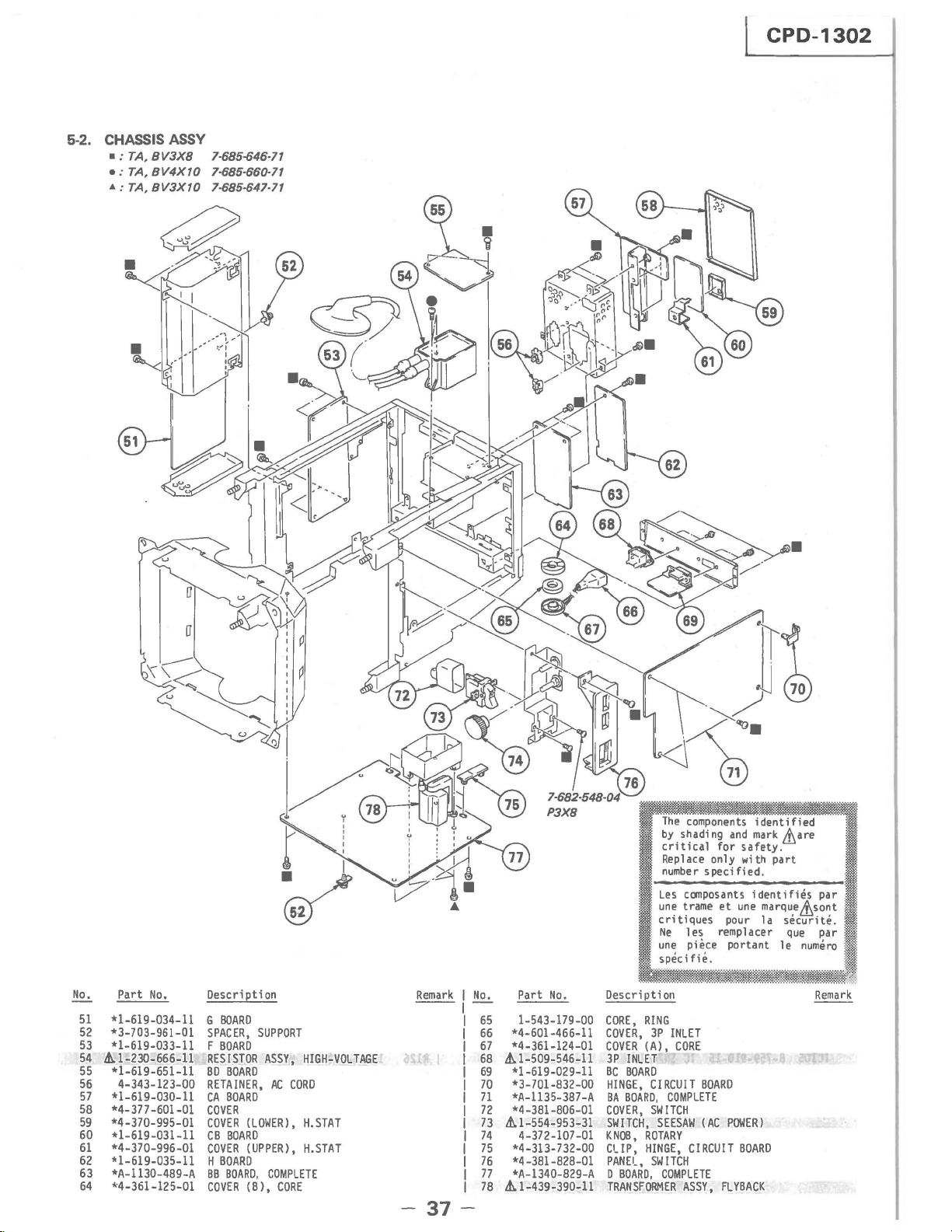
5-2.
CPD-1302
7-685-646-71
7-685-660-71
7-685-647-71
Part
~
*1-619-034-11
51
*3-703-961-01
52
*1-619-033-11
53
~
1
54
a;1:619-651-11
55
4 343-123-00
56
*1:619-030-11
57
*4-377-601-01
58
*4-370-995-01
59
*1-619-031-11
60
*4-370-996-01
61
*1-619-035-11
62
*A-1130-489-A
~~
*4-361-125-01
No.
230-666-11
Description
~P~~~~
F
RESISTOR
8D
RETAINER,
CA
COVER
COVER
C8
COVER
H
BB
COVER
SUPPORT
BOARD
A ,
BOARD
SSY
HIGH-VOLTAGE
AC
CORD
80ARD
(LOWER)
80AR(DUPPER)
BOA:~D
BO
(8')
H.STAT
,
H.STAT
,
COMPLETE
CORE
,
Remark
--
37
I
~
I
65
I
66
I
67
I
68
II
69
I
70
I
71
I
72
I
73
I
74
(
75
I
76
I
~~
-
Part
No.
3
179-00
1-54 -
*4-601-466*4-361-124-
,1>1-509-5:::
*1-619-0
*3-701-8 -
·'-1135-387-'
*4-381-806-01
&"1-554-953-31
4-372-107-01 ClIP,
*4
313-732-00
.4
:381-828-01
*A-1340-829-A
&'1-439-390-11
32
11
01
11
11
00
.
•..
The
com~one~~~
by
s~adlng
critlcal
Rep 1 ace
number
sp
Les
composart~ne
une trame e 1 a
..
Crltlque
Ne
une Pl
specifieo
Description
CORE,
R~~G
COVER,
COVER
(A),
3P
INLET
Be
BOARD
HINGE,
CI
BA
BOARD,
COVER,
5WITCH
SWITCH,
KNOB,
:'
TRANSFORMER
SEESAW
ROTARY I RCUIT
HINGE,
-NEI
SWITCH
BOARD,
CIlMP~~~E
s pour
1
es
.0
eoc
INLET
CORE
RCUIT
BOARD
COMPLETE
(AC
C
A ,
•
identified
mark
safety.
with
fi
ed
0
identifies
marque
lacer
BOARD
Ltare
part
.
p ,
Ltso~t
securl
teo .
par'
que . ;
r
f~
o~c~
remp 1 e numero .
e
portant
POWER'
FL
'BACK
: :
ar
CP,D-1302
SECTION 6
ELECTRICAL
PARTS LIST
NOTE:
Ref.No.
BB1
BB2
SS3
BB4
C101
C102
C103
C104
C105
C106
..c107
C108
C109
C110
Cll1
C112
C1l3
0101
0102
0103
0104
0105
0106
0107
0108
0109
0110
0111
0112
0113
0114
IC101
IC102
IC103
IC104
IC105
10
IC
9
0101
0102
0103
0104
The
components
by
shading
critical
Replace
number
Les
une
critiques
Ne
une
and
for safety.
only
specified.
compos
ants identifies par
trame
et
pour
les remplacer
piece portant
specifi.!.
Part
No.
*A-1130-489-A
CONNECTOR
*1-564-441-11
*1-564-440-11
*1-564-443-11
*1-564-443-11
CAPACITOR
1-102-959-00
1-102-959-00
1-102-959-00
1-102-959-00
1-102-959-00
1-102-959-00
1-102-959-00
1-102-959-00
1-124-445-00
1-124-445-00
1-124-478-11
1-124-902-00
1-124-927-11
DIODE
8-719-911-19
8-719-911-19
8-719-911-19
8-719-911-19
8-719-911-19
8-719-911-19
8-719-911-19
8-719-911-19
8-719-911-19
8-719-9ll-19
8-719-911-19
8-719-911-19
8-719-911-19
8-719-911-19
IC
8-759-904-81
8-759-904-81
8-759-910-15
8-759-910-15
8-759-910-15
8-759-917-52
TRANSISTOR
8-729-110-52
8-729-110-52
8-729-110-52
8-729-110-52
identified
mark
&are
with
part
une
marque&sont
la securite.
que
par
Ie
numero
Description
BB
BOARD,
COMPLETE
******************
PLUG,
CONNECTOR
PLUG,
CONNECTOR
PLUG, .CONNECTOR
PLUG,
CONNECTOR
CERAMIC
CERAMIC
CERAMIC
CERAMIC
CERAMIC
CERAMIC
CERAMIC
CERAMIC
ELECT
ELECT
ELECT
ELECT
ELECT
DIODE
lSS119
DIODE
lSS119
DIODE
lSS119
DIODE
lSS119
DIODE
lSS119
DIODE
lSS119
DIODE
lSS119
DIODE
lSS119
DIODE
lSS119
DIODE
lSS119
DIODE
lSS119
DIODE
lSS119
DIODE
lSS119
DIODE
lSS119
IC
74F08PC
IC
74F08PC
IC
SN74S15N
IC
SN74S15N
IC
SN74S15N
IC
74Fl38PC
TRANSISTOR
TRANSISTOR
TRANSISTOR
TRANSISTOR
2SA1005-L
2SA1005-L
2SA1005-L
2SA1005-L
•
•
(2.5MM)
(2.5MM)
(2.
(2.5MM)
22PF
22PF
22PF
22PF
22PF
22PF
22PF
22PF
100MF
100MF
100MF
0.47MF
4.7MF
5MM)
ltems
marked
since
routine service.
anticipated
All
variable
have
characteristic
otherwise noted.
CAPACITORS
MF
:)J
F,
they
PF
"*"
are
when
and
:)J
Remark
--1--
5P
4P
7 P
7P
5%
50V
5%
50V
5%
50V
5%
50V
5%
50V
5%
50V
5%
50V
5%
50V
20%
16V
20%
16V
20%
25V
20%
50V
20%
50V
are
not
seldom
Some
delay
ordering these items.
stocked
required for
should
adjustable resistors
curve
B,
unless
)J F
IRef.No.
1
0105
0106
0107
0108
0109
0110
0111
0112
0113
0114
0115
0116
0117
0118
0119
0120
0121
R101
R102
R103
R104
R105
R106
R107
R108
R109
R110
RIll
R112
R113
R114
R115
R116
R117
R118
R119
R120
R121
R122
R123
R124
R125
R126
R127
R128
R129
R130
R131
R132
R133
R134
Part
8-729-110-52
8-729-110-52
8-729-110-52
8-729-110-52
8-729-603-30
8-729-603-30
8-729-603-30
8-729-603-30
8-729-603-30
8-729-603-30
8-729-603-30
8-729-603-30
8-729-603-30
8-729-603-30
8-729-603-30
8-729-603-30
8-729-603-30
1-249
1-249-425-11
1-249-425-11
1-249-425-11
1-249-429-11
1-249-425-11
1-249-419-11
1-249-429-11
1-249-433-11
1-249-425-11
1-249
1-249-425-11
1-249-433-11
1-249-425-11
1-249-425-11
1-215-423-00
1-215-423-00
1-215-423-00
1-215-423-00
1-215-423-00
1-215-423-00
1-215-423-00
1-215-423-00
1-215-403-00
1-215-403-00
1-215-403-00
1-215-403-00
1-215-403-00
1-215-403-00
1-215-403-00
1-215-403-00
1-215-413-00
1-215-413-00
1-215-413-00
be
No.
-429-11
-4
29-11
RESISTORS
All
resistors are
F :
nonflammable
COILS
•
r+lH
: nil,
When indicating
ence
number,
the
board
Description
TRANSISTOR
TRANSISTOR
TRANSISTOR
TRANSISTOR
TRANSISTOR
TRANSISTOR
TRANSISTOR
TRANSISTOR
TRANSISTOR
TRANSISTOR
TRANSISTOR
TRANSISTOR
TRANSISTOR
TRANSISTOR
TRANSISTOR
TRANSISTOR
TRANSISTOR
RESISTOR
CARBON
CARBON
CARSON
CARBON
CARBON
CARBON
CARBON
CARBON
CARBON
CARBON
CARBON
CARBON
CARBON
CARBON
CAR80N
METAL
METAL
METAl.
METAL
METAL
METAl.
METAL
METAL
METAL
METAL
METAL
METAL
METAL
METAL
METAL
METAL
METAL
METAL
METAL
UH
: )J H
parts
please include
name.
2SA1005-L
2SA1005-L
2SA1005-L
2SA1005-L
2SC403SP-3
2SC403SP-3
2SC403SP-3
2SC403SP-3
2SC403SP-3
2SC403SP-3
2SC403SP-3
2SC403SP-3
2SC403SP-3
2SC403SP-3
2SC403SP-3
2SC403SP-3
2SC403SP-3
10K
4.7K
4.7K
4.7K
10K
4.7K
1.5K
10K
22K
4.7K
10K
4.7K
22K
4.7K
4.7K
1.2K
1.2K
1.2K
1.2K
1.2K
1.2K
1.
2K
1.2K
180
180
180
180
180
180
180
180
470
470
470
in
ohms
by
5%
5%
5%
5%
5%
5%
5%
5%
5%
5%
5%
5%
5%
5%
5%
1%
1%
1%
1%
1%
1%
1%
1%
1%
1%
1%
1%
1%
1%
1%
1%
1%
1%
1%
refer·
1/6W
1/6W
1/6W
1/6W
1/6W
1/6W
1/6W
1/6W
1/6W
1/6W
1/6W
1/6W
1/6W
1/6W
1/6W
1/6W
1/6W
1/6W
1/6W
1/6W
1/6W
1/6W
1/6W
1/6W
1/6W
1/6W
1/6W
1/6W
1/6W
1/6W
1/6W
1/6W
1/6W
1/6W
Remark
38
-
CPD-1302
IBBIIBDI
Ref
R135
R136
R137
R138
R139
R140
R141
R142
R143
R144
R145
R146
R147
R148
R149
R150
R151
R152
R153
R154
R155
R156
R157
R158
R159
R160
R161
R162
R163
R164
R165
R166
R167
R168
R169
R170
Rl71
R172
R173
R174
R175
R176
Rl77
R178
R179
R180
R181
R182
R183
R184
R185
R186
R187
.No.
Part
1-215-413-00
1-215-413-00
1-214-721-00
1-215-413-00
1-215-4i3-00
1-249-419-11
1-249-419-11
1-249-419-11
1-249-419-11
1-249-419-11
1-249-419-11
1-249-419-11
1-249-419-11
1-215-423-00
1-215-431-00
1-215-431-00
1-215-423-00
1-215-431-00
1-215-431-00
1-215-423-00
1-215-423-00
1-215-431-00
1-214-739-00
1-247-833-00
1-247-833-00
1-249-419-11
1-249-419-11
1-249-419-11
1-249-433-11
1-247-839-00
1-247-829-00
1-247-829-00
1-247-829-00
1-249-433-11
1-249
1-249-433-11
1-249-429-11
1-249-425-11
1-249-425-11
1-247-708-11
1-249-441-11
1-249-423-11
1-249-423-11
1-249-423-11
1-247-823-00
1-247
1-247-823-00
1-247-823-00
1-247-804-00
1-247-823-00
1-247-823-00
1-247-104-00
1-247-823-00
No.
-43
-804
3-11
-00
Description
METAL
METAL
METAL
METAL
METAL
CARBON
CARBON
CARBON
CARBON
CARBON
CARBON
CARBON
CARBON
METAL
METAL
METAL
METAL
METAL
METAL
METAL
METAL
METAL
METAL
CARBON
CARBON
CARBON
CARBON
CARBON
CARBON
CARBON
CARBON
CARBON
CARBON
CARBON
CARBON
CARBON
CARBON
CARBON
CARBON
CARBON
CARBON
CARBON
CARBON
CARBON
CARBON
CARBON
CARBON
CARBON
CARBON
CARBON
CARBON
CARBON
CARBON
470
470
470
470
470
1.5K
1.5K
1.5K
1.5K
1.
5K
1.
5K
1.5K
1.5K
1.2K
2.7K
2.7K
1.2K
2.7K
2.7K
1.2K
1.2K
2.7K
2.7K
1.2K
1.2K
1.5K
1.
5K
1.5K
22K
2.2K
820
820
820
22K
22K
22K
10K
4.7K
4.7K
470
lOOK
3.3K
3.3K
3.3K
470
75
470
470
75
470
470
75
470
1%
1/6W
1%
1/6W
1%
1/4W
1%
1/6W
1/6W
1%
5%
l/6W
5%
1/6W
5%
1/6W
5%
1/6W
5%
1/6W
5%
1/6W
5%
1/6W
5%
1/6W
1%
l/6W
1%
1/6W
1%
l/6W
1%
1/6W
1%
1/6W
1%
1/6W
1%
1/6W
1%
l/6W
1%
l/6W
1%
1/4W
5%
1/6W
5%
1/6W
5%
l/6W
5%
l/6W
5%
1/6W
1/6W
5%
5%
1/6W
5%
l/6W
5%
1/6W
5%
1/6W
5%
1/6W
5%
1/6W
5%
1/6W
5%
1/6W
5%
1/6W
5%
1/6W
5% 1/4W
5%
1/6W
5%
1/6W
5%
1/6W
5%
l/6W
5% 1/6W
5%
1/6W
1/6W
5%
5%
1/6W
5%
1/6W
1/6W
5%
5%
l/6W
5%
1/4W
1/6W
5%
Remark
--1--
IRef.No. Part
1
R188
1
R189
1
******************************************************
BD1
BD2
C203
C204
C206
C208
C213
C214
C263
C266
e271
C276
C277
C285
C287
0202
0203
IC204
IC206
Q201
Q202
Q203
Q204
Q261
Q262
Q263
Q264
Q271
Q272
Q273
Q274
Q275
No.
1-249-429-11
1-249-417-11
*A-1130-510-A
CONNECTOR
*1-564-440-11
*1-564-441-11
CAPACITOR
1-124-443-00
1-102-074-00
1-101-004-00
1-123-607-00
1-124-927-11
1-10 1-001-00
1-124-902-00
1-124-927-11
1-124-445-00
1-124-907-00
1-108-622-91
1-106-196-00
1-106-212-00
DIODE
8-719-911-19
8-719-911-19
IC
8-759-900-86
8-759-902-21
TRANSISTOR
8-729-178-54
8-729-178-54
8-729-178-54
8-729-900-36
8-729-104-80
8-729-178-54
8-729-178-54
8-729-178-54
8-729-178-54
8-729-178-54
8-729-178-54
8-729-900-80
8-729-900-36
Description
CARBON
CARBON
BD
BOARD,
******************
P'_UG,
CONNECTOR
PLUG,
CONNECTOR ( 2.5MM)
ELECT
CERAMIC
CERAMIC
ELECT
ELECT
CERAMIC
ELECT
ELECT
ELECT
ELECT
MYLAR
MYLAR
MYLAR
DIODE
155119
DIODE
155119
IC
SN74LS86N
IC
SN74LS221N
TRANSISTOR
TRANSISTOR
TRANSISTOR
TRANSISTOR
TRANSISTOR
TRANSISTOR
TRANSISTOR
TRANSISTOR
TRANSISTOR
TRANSISTOR
TRANSISTOR
TRANSISTOR
TRANSISTOR
10K
1K
COMPLETE
(2.5MM)
100MF
O.OOlMF
O.OlMF
O.lMF
4.7MF
O.OOlMF
0.47MF
4.7MF
100MF
10MF
0.0047MF
O.OlMF
0.047MF
2SC2785
2SC2785
2SC2785
DTC124ES
2SC3355
2SC2785
2SC2785
2SC2785
2SC2785
2SC2785
2SC2785
DTC114ES
DTC124ES
5%
5%
4P
5P
20%
10%
20%
20%
20%
20%
20%
20%
10%
10%
10%
1/6W
1/6W
Remark
*******~
10V
50V
50V
50V
50V
50V
50V
50V
16V
50V
100V
100V
100V
-
39-
 Loading...